Article

Electrodeposition of Copper Oxides as Cost-Effective Heterojunction Photoelectrode Materials for Solar Water Splitting

1
College of Photonics, National Yang Ming Chiao Tung University, Tainan 71150, Taiwan
2
Clean Energy Conversion Research Center, Institute for Advanced Engineering, Yongin 17180, Republic of Korea
3
Green Energy and Environment Research Laboratories, Industrial Technology Research Institute, Tainan 71150, Taiwan
*
Authors to whom correspondence should be addressed.
These authors contributed equally to this work.
Coatings 2022, 12(12), 1839; https://doi.org/10.3390/coatings12121839
Submission received: 28 October 2022 / Revised: 24 November 2022 / Accepted: 25 November 2022 / Published: 28 November 2022
(This article belongs to the Special Issue Advanced Electrochemical Surface Properties)

Abstract

:
Photoelectrocatalytic hydrogen production is crucial to reducing greenhouse gas emissions for carbon neutrality and meeting energy demands. Pivotal advances in photoelectrochemical (PEC) water splitting have been achieved by increasing solar light absorption. P-type Cu-based metal oxide materials have a wide range of energy band gaps and outstanding band edges for PEC water splitting. In this study, we first prepared Cu2O thin films using electrodeposition and fabricated a heterojunction structure of CuO/Cu2O by controlling annealing temperatures. The surface morphological, optical, and electrochemical properties were characterized using various analytical tools. X-ray and Raman spectroscopic approaches were used to verify the heterojunction of CuO/Cu2O, while surface analyses revealed surface roughness changes in thin films as the annealing temperatures increased. Electrochemical impedance spectroscopic measurements in conjunction with the Mott–Schottky analysis confirm that the CuO/Cu2O heterojunction thin film can boost photocurrent generation (1.03 mA/cm2 at 0 V vs. RHE) via enhanced light absorption, a higher carrier density, and a higher flat band potential than CuO and Cu2O thin films (0.92 and 0.08 mA/cm2, respectively).

1. Introduction

Solar energy is one of the most viable renewable energy resources to meet global energy demand and minimize environmental pollution and global warming [1]. Effective solar energy harvesting has been a central direction in improving photoconversion efficiencies [2,3,4]. Among solar energy-driven approaches for producing green hydrogen, photoelectrochemical (PEC) water splitting has attracted significant attention [5]. Briefly, it generates electron-hole pairs via a semiconductor photoelectrode by absorbing sunlight and separating the charges that go to the photoelectrodes. Then, the reduction and oxidation processes of water on the electrodes by charge carriers occur, producing hydrogen and oxygen [6]. To date, many photoelectrode materials for PEC water splitting have been designed, including TiO2 [7,8], Fe2O3 [9,10], BiVO4 [11,12], Si [13,14], Cu2O [15,16], and CuO [17,18]. Photoelectrodes for PEC water splitting must have a suitable energy band gap [5]. For example, the energy of the conduction band (CB) should be lower than that of reduced water, while that of the valence band (VB) should be higher than that of oxidized water. In particular, p-type semiconducting copper oxides (i.e., Cu2O and CuO) have a low energy band gap (2.0–2.5 eV [19,20,21] and 1.3–2.1 eV [20,22,23], respectively). It is also known that they are a potential electrode material for photovoltaic applications [24] because of their cost-effectiveness, non-toxicity, excellent carrier mobility [25], and high absorption coefficient. Similarly, these advantages make copper oxides suitable as an efficient photoelectrode for PEC water splitting, as shown in Table S1 [26,27,28,29,30,31,32,33,34,35,36,37] and Table S2 [38,39,40]. One crucial obstacle to copper oxides may be their high electron-hole recombination rate, lowering photoconversion efficiencies. One of the effective approaches to address the issue is to employ a heterostructure configuration with a non-copper-containing semiconductor material, for example, Fe2O3/CuO [41,42], CuO/ZnO [43], TiO2/CuO [44], WO3/Cu2O [45], InGaN/Cu2O [46], and Cu2O/g-C3N4/Cu2O [47]. Although the heterojunction structures reduce the electron-hole recombination rate, they also increase the complexity of devices. Accordingly, heterostructured CuO/Cu2O, which has been proposed as the heterojunction configuration, can be prepared using simple thermal oxidation from Cu2O (Cu2O + 1/2O2 → 2CuO) [28]. In this work, we reported a facile method to prepare a CuO/Cu2O heterojunction structure for PEC water splitting. Cu2O thin films were prepared by electrodeposition, and thermal treatment was performed [28,40,48]. Simple and eco-friendly electrodeposition by controlling annealing temperatures resulted in micron thick copper oxide layers (~1.4 μm thick) compared to physical methods (i.e., sputtering and pulsed laser deposition). Controlling thin-film thicknesses is one of the essential design factors to improve electron-hole separation [49,50]. The heterojunction configuration demonstrated improved PEC performance compared to CuO and Cu2O, as confirmed by the analysis of X-ray diffraction (XRD), X-ray photoelectron spectroscopy (XPS), ultraviolet-visible (UV-Vis) spectroscopy, electrochemical impedance spectroscopy (EIS), and Raman spectroscopy. In particular, copper oxide thin films were characterized to understand the change in carrier densities and flat-band potentials.

2. Experimental Details

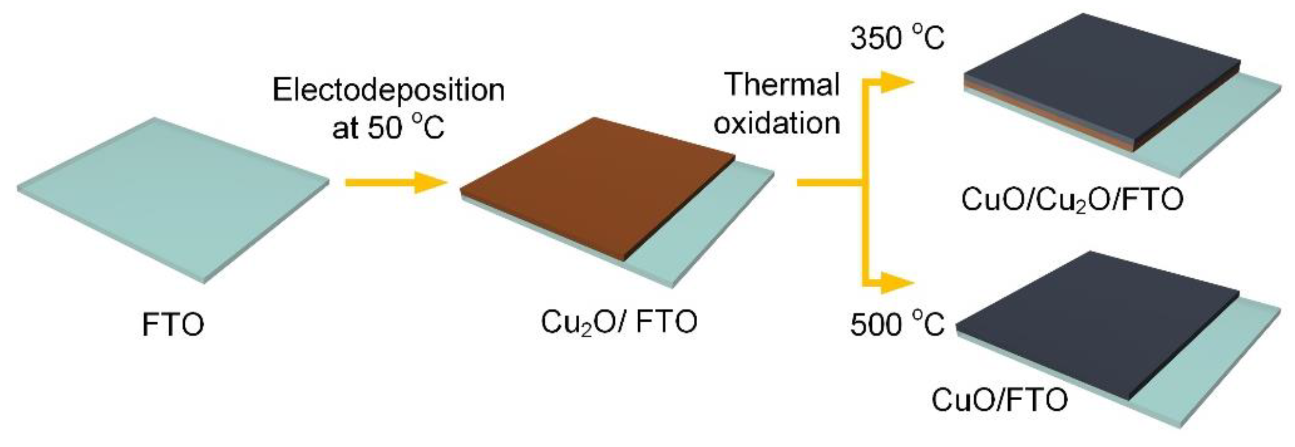
2.1. Fabrication of Copper Oxide Thin Films

Cu2O thin films were prepared by electrodeposition on fluorine-doped tin oxide glass substrates (FTO, ~400 nm and 1 cm × 2 cm). The substrates were first cleaned with an ultrasonicator with acetone, isopropyl alcohol (IPA), ethanol, and deionized (DI) water for 5 min and dried in an oven. In this study, all chemicals and reagents were used without further purification. Electrodeposition was performed using a three-electrode system with a potentiostat (SP-150e, BioLogic, Seyssinet-Pariset, France). A cleaned FTO substrate, a coiled platinum wire (0.5 mm diameter), and Ag/AgCl (3 M NaCl) were used as working, counter, and reference electrodes, respectively. Copper sulfate (Sigma-Aldrich, Burlington, MA, USA, >98%) and 3M lactic acid (Sigma-Aldrich, Burlington, MA, USA, >85%) mixed in 40 mL of DI water were used after adjusting pH = 9 with 5 M NaOH. The chronoamperometric (CA) method was applied at −0.36 V (V vs. Ag/AgCl) for 20 min to deposit Cu2O thin films on an FTO glass substrate at ~50 °C and with magnetic stirring at 600 rpm. We then carried out thermal oxidation at different temperatures for 1 h on a hot plate using as-prepared Cu2O thin films after washing with DI water and drying with nitrogen. After conducting the annealing temperature effects, we found that heterostructured CuO/Cu2O/FTO and CuO/FTO thin films can be prepared at 350 and 500 °C, respectively (Figure 1). For simplicity, Cu2O, CuO/Cu2O, and CuO thin films correspond to Cu2O/FTO prepared by electrodeposition without annealing, a heterostructured configuration of CuO/Cu2O/FTO annealed at 350 °C and CuO/FTO annealed at 500 °C.

2.2. Materials Characterization

The surface morphologies of three thin films (Cu2O, CuO/Cu2O, and CuO deposited on an FTO-coated glass substrate) were observed by scanning electron microscopy (SEM, Zeiss Gemini 450, Jena, Germany) operated at an acceleration voltage of 10 keV. Ultraviolet-visible spectroscopy (UV-VIS, SEMSO-3000, AUBOTECH, Taipei, Taiwan) was used to examine the optical properties of the thin films. X-ray diffraction (XRD, Brucker D8 DISCOVER, Billerica, MA, USA) with Cu Kα radiation (λ = 0.154184 nm) and Raman microscopy (CL Technology UniDRON-S, New Taipei, Taiwan) with a 532 nm excitation wavelength were applied to investigate the transformation of Cu2O to CuO. An X-ray photoelectron spectrometer (XPS, Thermo Scientific K-Alpha, Waltham, MA, USA) was used with monochromatic Al Kα radiation and a flood gun to examine the chemical valences of the thin films. All electrochemical measurements were performed using a standard rectangular quartz cuvette of ~20 mL with the three-electrode system. A leakless miniature Ag/AgCl reference electrode (ET072-1, eDAQ, 3.4 M KCl) was used after calibration using the Ag/AgCl (3 M NaCl) reference electrode to convert the potentials to the reversible hydrogen electrode (RHE) scale [51]. While 0.2 M Na2SO4 (pH = 6.2) was used as an electrolyte, an active area of thin films of 1.0 cm2 was set using a chemical-tolerant 3 M tape (Electroplating Tape 470, 3 M). For the Mott–Schottky analysis, the frequency was set at 1k Hz and an amplitude of 10 mV. For PEC measurements, potentials were applied from 0 to 0.5 V (vs. RHE) at the scan rate of 5 mV/s. A solar simulator with an AM 1.5 G filter (Enlitech SS-X, Enlitech, Kaohsiung, Taiwan) and a light intensity of 100 mW/cm2 was used as a light source after accurate calibration. The EIS was also adopted to ensure the rate of charge-transfer reactions between the electrode surface and the electrolyte. The Nyquist plots were obtained by applying a static potential of 0.3 V vs. Ag/AgCl with the 5 mV sinusoidal wave from 0.1 to 1 M Hz without and with light illumination.

3. Results and Discussion

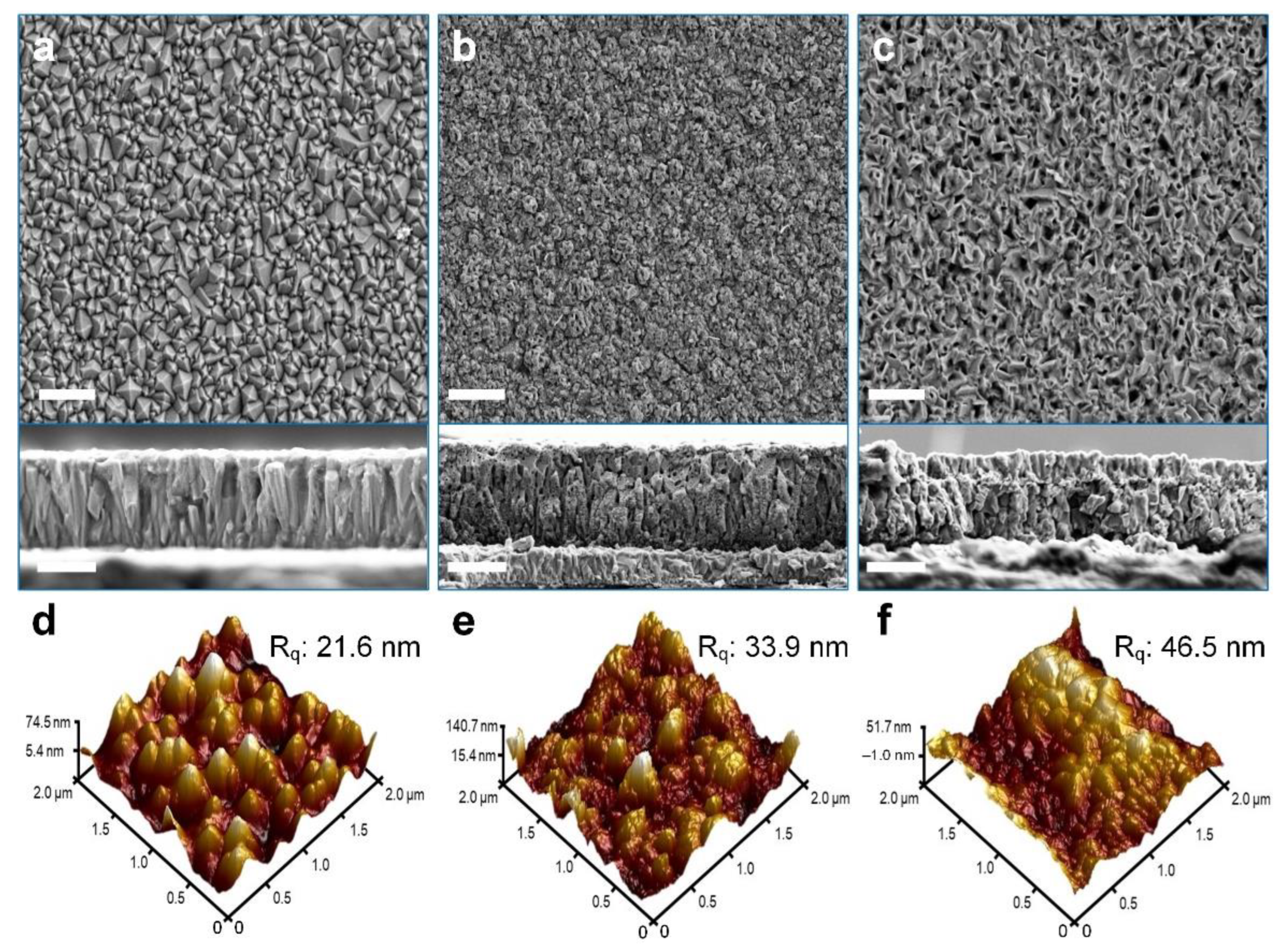
3.1. Morphology and Optical Properties of Copper Oxide Thin Films

The surface morphologies of the thin films were examined by SEM and AFM, as shown in Figure 2. After 1-h thermal treatment at 350 and 500 °C, it was observed that the grain sizes and shapes changed, and the surfaces became denser than pristine Cu2O thin films. The cross-sectional view of the Cu2O thin film indicates a thickness of ~1.40 μm. Due to the difference in density (Cu2O: 6.0 g/cm3 and CuO: 6.31 g/cm3) [52] and the thermal expansion of Cu2O [53] after thermal oxidation (Cu2O + 1/2O2 → 2CuO), a slight increase in thickness was observed, similar to previous reports [28]. As summarized in Table S3, energy-dispersive X-ray spectroscopy (EDS) was also employed to examine the chemical composition of the thin films before and after annealing at 350 and 500 °C. It verifies the successful fabrication of Cu2O using electrodeposition and the complete transformation of Cu2O to CuO after annealing at 500 °C for 1 h. Additionally, the EDS analysis shows a heterostructure of CuO/Cu2O ([Cu]/[O] = 1.52). The SEM analysis illustrates that the annealing of metal oxides [54] led to the agglomeration of adjacent grains [55].
A similar trend was also observed using AFM (Figure 2d–f), which is attributed to the random distribution of grains and phase changes [56]. It was found that the root mean square (RMS) roughness of the thin films increased from 21.6 nm (Cu2O) to 33.9 nm (CuO/Cu2O at 350 °C) and 46.5 nm (CuO at 500 °C) (Cu2O < CuO/Cu2O < CuO). We assume that the controlling of thin film thicknesses using the electrolyte temperature affects RMS roughness [40]. Furthermore, since the light absorption properties of thin films play an essential role in PEC performance, we measured the absorbance of Cu2O, CuO/Cu2O, and CuO thin films using a UV-Vis spectrometer. Figure 3a shows the typical absorbance of the three thin films, demonstrating that the Cu2O thin film has an absorption edge in the range of 500 to 650 nm. It shows that the absorption edge of thermally treated thin films (CuO/Cu2O and CuO) was red-shifted. In addition, we measured the band gaps of these samples using the Tauc plot analysis [57] using ( α h ν ) n = B ( h ν E g ) , where α is the absorption coefficient, h is the Plank constant, v is the photon energy, B is a constant, and Eg is the band gap. The copper oxide thin films were analyzed with a direct transition (n = 2). As Figure 3b and Table S4 show, the band gaps measured (Cu2O: 2.35 eV, CuO/Cu2O: 1.81 eV, CuO: 1.45 eV) are in good agreement with a previous study [28]. CuO/Cu2O and CuO exhibited a higher band gap than Cu2O, denoting that they can expand the absorption range of visible light compared to Cu2O. Consequently, it could improve PEC performance [58].

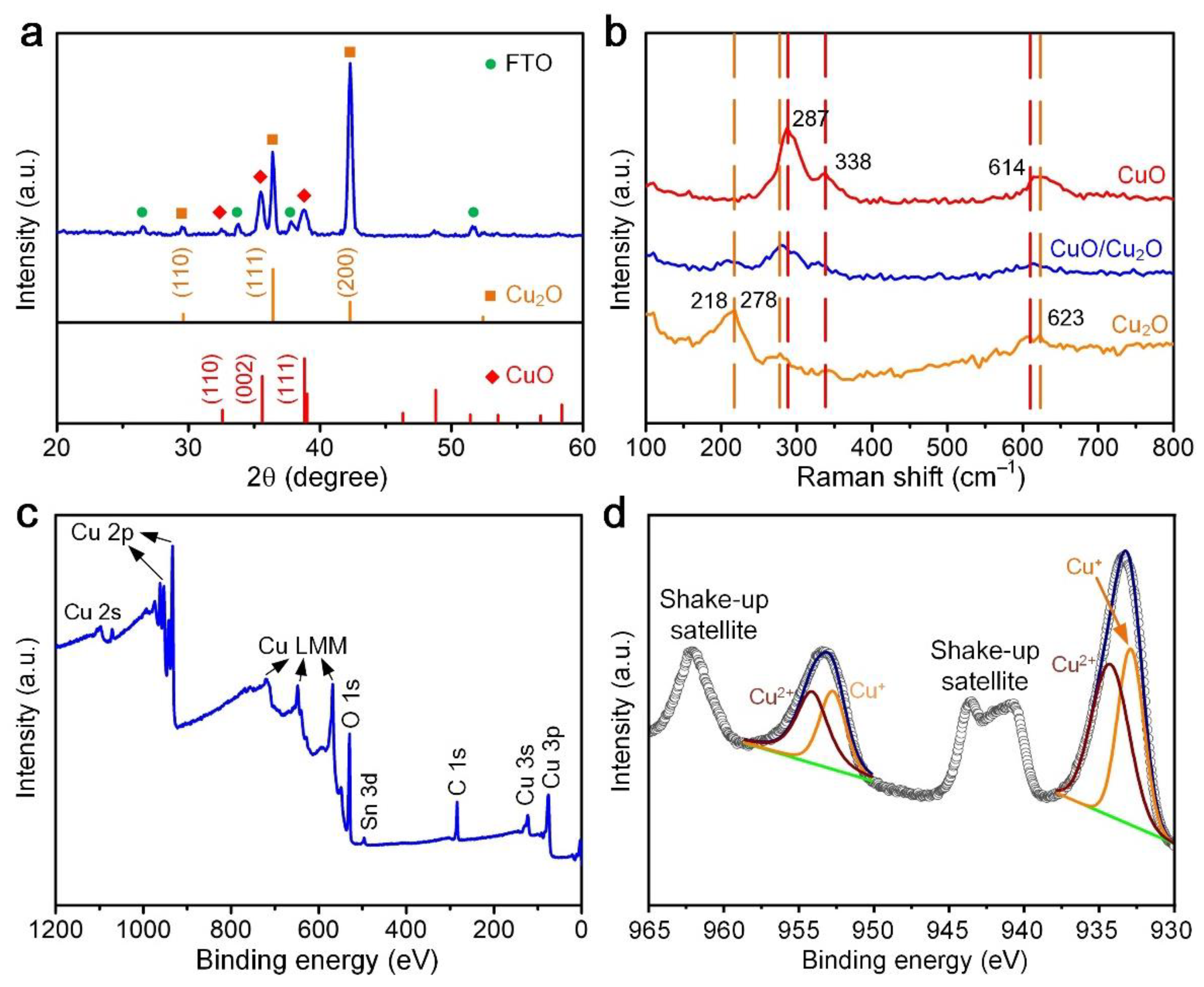
3.2. Characterization of Copper Oxide Thin Films Using XRD, Raman Spectroscopy, and XPS

Figure 4a demonstrates the XRD pattern for the CuO/Cu2O thin film, while Figure S1 shows those for Cu2O and CuO thin films. For the Cu2O thin film, the peaks at 36.6° and 42.5° are attributed to the (111) and (200) planes [59,60] (JCPDS file No. 99-0041). The XRD pattern of Cu2O illustrates that the thin films exhibit the (200) plane as the preferential growth direction [61]. Cu2O and CuO diffraction peaks were observed in the thin film annealed at 350 °C, while the thin film annealed at 500 °C exhibited the pure CuO phase (JCPDS file No. 72-0269) [62]. The distinctive diffraction peak at 35.6° indicates that the thin film has a good crystal structure of CuO after annealing at 500 °C. The XRD analysis may support that the thermal oxidation process at 350 °C produced heterostructured CuO/Cu2O similar to the previous studies [28,63]. The particle sizes of the thin films were evaluated using the Scherrer–Debye equation [64], D = K λ β cos θ , where D is the average crystal particle size, K is a constant, λ is the wavelength of X-ray, β is the full width at half maximum (FWHM), and θ is the Bragg angle. The Cu2O and CuO thin films were determined as 22.3 and 29.1 nm, respectively, indicating the improvement of the homogeneity of the thin films and the enhancement of the electrical properties [65]. As shown in Figure 4b, we also performed Raman spectroscopic measurements in the spectral region of 100 to 800 cm−1 to complement the XRD and SEM analyses. Single-phase Cu2O has only one Raman active mode (F2g), while single-phase CuO has three Raman active modes (Ag + 2Bg) [66]. The Raman bands of the Cu2O thin film at 218, 278, and 623 cm−1 are contributed from the second-order Raman-allowed modes of single-phase Cu2O [67], while those of the CuO thin film at 287, 338, and 614 cm−1 are in good agreement with single-phase CuO, as reported in the literature [68]. As the annealing temperatures increased, Cu2O peaks decreased, and CuO peaks appeared gradually. The Raman spectrum of the CuO/Cu2O thin film shows that the combined peaks of Cu2O and CuO (209, 279, 329, and 614 cm−1) are assigned to the Ag and Bg modes [66]. As illustrated in Figure 4c,d, XPS was also used to analyze the elemental compositions of copper oxides. Figure 4c shows a representative XPS survey spectrum of the CuO/Cu2O thin film [69]. All XPS spectra were calibrated with the C 1s photoemission peak of adventitious carbon at 284.5 eV [70]. Figure S2a,b shows the XPS spectra of Cu 2p of the Cu2O and CuO thin films that align with those reported in the literature [71,72]. To examine the heterostructure of the CuO/Cu2O thin film, we carried out the deconvolution of its XPS spectrum using XPSPEAK 4.1. Two main peaks and satellite peaks were observed in the spectrum. The deconvolution process identified that the peaks at 932.91 and 952.74 eV are related to Cu+ (Cu2O), which are assigned to Cu 2p3/2 and Cu 2p1/2. By contrast, those at 934.27 and 954.12 eV are attributed to Cu 2p3/2 and Cu 2p1/2, confirming the presence of Cu2+ (CuO). As summarized in Figure S2c, we observed a slightly broadened peak for Cu 2p3/2 of CuO/Cu2O compared to CuO. Based on the deconvolution of the CuO/Cu2O thin film, we manifested that the sample is a heterojunction (CuO:Cu2O = 56.4%:43.6%), which qualitatively agrees with the analysis using SEM/EDS (Table S3). As reported [73,74], metal oxide thin films fabricated via simple annealing could generate cracks inside thin films due to thermal stress, enabling X-ray beams to irradiate the FTO surface. Thus, the peak at 496.08 eV can be assigned to Sn 3d originating from FTO [75]. We assumed that the CuO/Cu2O thin film prepared by electrodeposition could become a heterojunction configuration as reported [28] according to the characterization of the SEM/EDS, XRD, XPS, and Raman spectroscopic analyses.

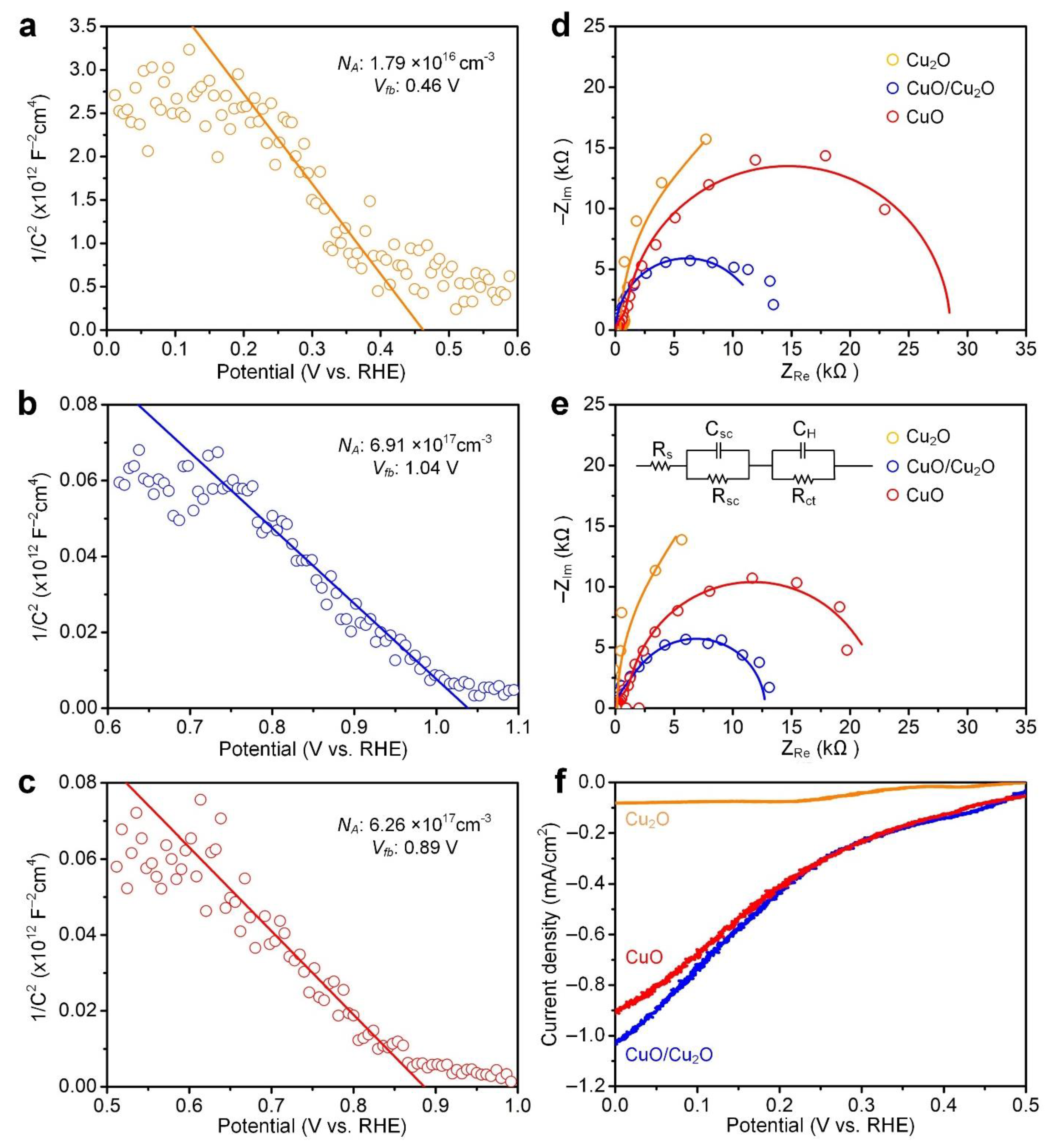
3.3. Electrochemical Measurements of Copper Oxide Thin Films

The Mott–Schottky technique was applied to examine changes in electrochemical interfaces between the electrolyte and photocathodes prepared in this study. Carrier densities and flat band potentials can be accurately measured using the Mott–Schottky equation for p-type semiconductors [76,77].
1 C 2 = 2 ε ε 0 e N A A 2 ( V V f b k B T e )
where C is the interfacial capacitance, ε is the dielectric constant of the semiconductor electrode, ε 0 is the vacuum permittivity, e is the electron charge, Vfb is the flat band potential, NA is the major carrier density, A is the electrode area, V is the applied voltage, kB is the Boltzmann constant, and T is the absolute temperature. Carrier densities of p-type copper oxides (NA) can be determined from a straight line by plotting 1/C2 vs. V, while the flat band potential (Vfb) can be obtained from the intercept with the x-axis. While carrier densities affect charge transfer rates [28,78,79], the flat band potential is associated with a driving force to separate electron-hole pairs in the space charge region, which can be used as one of the key factors to predict PEC performance. For example, a shift of the flat band to a more positive potential denotes improved electron transfer, decreasing the recombination of electron-hole pairs and boosting PEC efficiencies [80]. Figure 5a–c demonstrates Mott–Schottky plots for Cu2O, CuO/Cu2O, and CuO thin films. The three thin films exhibit p-type semiconductor characteristics with a negative slope. ε of 7.6 for Cu2O [81] and 10.26 [36] for CuO/Cu2O and CuO thin films were used to calculate carrier densities. It resulted in a NA value of 1.79 × 10¹⁶, 6.91 × 10¹⁷, and 6.26 × 1017 cm–3, respectively, in the order of Cu2O < CuO < CuO/Cu2O. Moreover, we also successfully confirmed the same trend of flat band potentials of 0.46, 1.04, and 0.89 V, respectively. According to the Mott–Schottky analysis, the improved PEC performance of the heterojunction structure of CuO/Cu2O can be rationally anticipated [28]. Figure 5d,e shows Nyquist plots of three thin films without and with illumination. It exhibited that the radius of the semicircle decreased with light illumination to the working electrode. It denotes that illumination accelerated the rate of the charge transfer reaction between the photoelectrode surface and the electrolyte, and accordingly, the carrier density increased. As shown in Figure 5e, EIS data were then analyzed by fitting with an equivalent electrical circuit model to examine transfer resistance on different photoelectrode materials. As reported, Rs is the series resistance, Rsc is the resistance on the depletion layer, and Rct is the charge transfer resistance, while Csc is the capacitance related to the depletion layer of a semiconductor and CH is the Helmholtz layer capacitance [82]. It is anticipated that the heterostructured electrode exhibits the lowest charge transfer resistance (Rct) due to its smallest diameter, leading to the highest charge transfer reaction rate [28]. Figure 5f illustrates representative photocurrent densities of three electrode materials under AM1.5G illumination. For the Cu2O thin film, a photocurrent of 0.08 mA/cm2 at 0 V (vs. RHE) was observed, while for the CuO/Cu2O and CuO thin films, the photocurrent increased to 1.03 and 0.92 mA/cm2, respectively. It aligns with Mott–Schottky and EIS-based analyses. Table 1 compiles carrier densities, flat band potentials, and photocurrent densities of Cu2O, CuO/Cu2O, and CuO thin films. It is noted that PEC performance can be affected by too high annealing temperatures, altering the electrical property of FTO-based thin films [83]. In summary, it manifests that a higher carrier density, a higher flat band potential, and lower charge transfer resistance of the heterojunction CuO/Cu2O thin film could be highly correlated with the PEC performance compared to the Cu2O and CuO thin films [28].

4. Conclusions

Cu2O thin films were effectively fabricated using electrodeposition, followed by controlling annealing temperatures. The thickness and morphology of thin films were analyzed using SEM, while the surface roughness was investigated using AFM. XRD, XPS, and Raman spectroscopic measurements confirmed the heterojunction structure of CuO/Cu2O after annealing at 350 °C. As the thermal oxidation temperatures increased, the light absorbance edge of the thin films was red-shifted, demonstrating a better absorber in the visible region and enhancing photocurrent densities in the order of Cu2O < CuO < CuO/Cu2O. In particular, the Mott–Schottky and EIS measurements confirmed that the heterojunction structure has a higher carrier concentration, a larger flat band potential, and a lower charge transfer resistance than the Cu2O and CuO thin films. Accordingly, the CuO/Cu2O thin film annealed at 350 °C achieved a boosted photocurrent density of 1.03 mA/cm2 at 0 V (vs. RHE). We demonstrated that the heterojunction configuration of copper oxide thin films (CuO/Cu2O) via the cost-effective electrodeposition method could improve PEC performance by reducing the electro-hole pair recombination and increasing carrier densities.

Supplementary Materials

The following supporting information can be downloaded at: https://www.mdpi.com/article/10.3390/coatings12121839/s1, Table S1: Compilation of copper oxide-based photocathodes used for PEC water splitting, Table S2: Compilation of heterostructured copper oxide-based photoelectrodes, Table S3: EDS analysis results of Cu2O, CuO/Cu2O, and CuO thin films, Table S4: Band gaps of Cu2O, CuO/Cu2O, and CuO thin films, Table S5: EIS parameters obtained by fitting the Nyquist plots with the equivalent circuit, Figure S1: XRD patterns of (a) Cu2O, (b) CuO/Cu2O, and (c) CuO thin films, Figure S2: XPS spectra for Cu 2p of (a) Cu2O and (b) CuO thin films and (c) comparison of CuO and CuO/Cu2O thin films.

Author Contributions

Conceptualization, Y.C.; data curation, T.-H.Y. and B.-J.L.; investigation, T.-H.Y., B.-J.L., Y.-W.L., Y.-S.L. and C.-W.L.; methodology, T.-H.Y. and B.-J.L.; project administration, C.C., H.-C.C. and Y.C.; software, T.-H.Y.; supervision, Y.C.; visualization, T.-H.Y., B.-J.L. and Y.-W.L.; writing original draft preparation, T.-H.Y., B.-J.L., Y.-W.L. and Y.-S.L.; writing—review and editing, Y.-P.L., C.C., H.-C.C. and Y.C. All authors have read and agreed to the published version of the manuscript.

Funding

We acknowledge the Bureau of Energy, Ministry of Economic Affairs, Taiwan (Grant No. 111-S0102). C.C. thanks the Ministry of Trade, Industry, and Energy (MTIE) of Korea for the Net-Zero Demand Management Program (KETEP 20212010200110).

Institutional Review Board Statement

Not applicable.

Informed Consent Statement

Not applicable.

Data Availability Statement

Not applicable.

Conflicts of Interest

The authors declare no conflict of interest.

References

  1. van Ruijven, B.J.; De Cian, E.; Wing, I.S. Amplification of future energy demand growth due to climate change. Nat. Commun. 2019, 10, 2762. [Google Scholar] [CrossRef] [Green Version]
  2. Abdin, Z.; Alim, M.A.; Saidur, R.; Islam, M.R.; Rashmi, W.; Mekhilef, S.; Wadi, A. Solar energy harvesting with the application of nanotechnology. Renew. Sust. Energ. Rev. 2013, 26, 837–852. [Google Scholar] [CrossRef]
  3. Guo, C.X.; Guai, G.H.; Li, C.M. Graphene based materials: Enhancing solar energy harvesting. Adv. Energy Mater. 2011, 1, 448–452. [Google Scholar] [CrossRef]
  4. Chang, S.-Y.; Cheng, P.; Li, G.; Yang, Y. Transparent polymer photovoltaics for solar energy harvesting and beyond. Joule 2018, 2, 1039–1054. [Google Scholar] [CrossRef] [Green Version]
  5. Minggu, L.J.; Daud, W.R.W.; Kassim, M.B. An overview of photocells and photoreactors for photoelectrochemical water splitting. Int. J. Hydrog. Energy 2010, 35, 5233–5244. [Google Scholar] [CrossRef]
  6. Ahmad, H.; Kamarudin, S.K.; Minggu, L.J.; Kassim, M. Hydrogen from photo-catalytic water splitting process: A review. Renew. Sust. Energ. Rev. 2015, 43, 599–610. [Google Scholar] [CrossRef]
  7. Lin, H.; Huang, C.P.; Li, W.; Ni, C.; Shah, S.I.; Tseng, Y.-H. Size dependency of nanocrystalline TiO2 on its optical property and photocatalytic reactivity exemplified by 2-chlorophenol. Appl. Catal. B 2006, 68, 1–11. [Google Scholar] [CrossRef]
  8. Yamada, Y.; Kanemitsu, Y. Determination of electron and hole lifetimes of rutile and anatase TiO2 single crystals. Appl. Phys. Lett. 2012, 101, 133907. [Google Scholar] [CrossRef] [Green Version]
  9. Xie, Y.; Ju, Y.; Toku, Y.; Morita, Y. Synthesis of a single-crystal Fe2O3 nanowire array based on stress-induced atomic diffusion used for solar water splitting. R. Soc. Open Sci. 2018, 5, 172126. [Google Scholar] [CrossRef] [Green Version]
  10. Sharma, P.; Jang, J.-W.; Lee, J.S. Key strategies to advance the photoelectrochemical water splitting performance of α-Fe2O3 photoanode. ChemCatChem 2019, 11, 157–179. [Google Scholar] [CrossRef]
  11. Sharp, I.D.; Cooper, J.K.; Toma, F.M.; Buonsanti, R. Bismuth vanadate as a platform for accelerating discovery and development of complex transition-metal oxide photoanodes. ACS Energy Lett. 2017, 2, 139–150. [Google Scholar] [CrossRef]
  12. Butler, K.T.; Dringoli, B.J.; Zhou, L.; Rao, P.M.; Walsh, A.; Titova, L.V. Ultrafast carrier dynamics in BiVO4 thin film photoanode material: Interplay between free carriers, trapped carriers and low-frequency lattice vibrations. J. Mater. Chem. 2016, 4, 18516–18523. [Google Scholar] [CrossRef] [Green Version]
  13. Bocarsly, A.B.; Bookbinder, D.C.; Dominey, R.N.; Lewis, N.S.; Wrighton, M.S. Photoreduction at illuminated p-type semiconducting silicon photoelectrodes. Evidence for Fermi level pinning. J. Am. Chem. Soc. 1980, 102, 3683–3688. [Google Scholar] [CrossRef]
  14. Luo, Z.; Wang, T.; Gong, J. Single-crystal silicon-based electrodes for unbiased solar water splitting: Current status and prospects. Chem. Soc. Rev. 2019, 48, 2158–2181. [Google Scholar] [CrossRef] [PubMed]
  15. Jin, Z.; Hu, Z.; Jimmy, C.Y.; Wang, J. Room temperature synthesis of a highly active Cu/Cu2O photocathode for photoelectrochemical water splitting. J. Mater. Chem. A 2016, 4, 13736–13741. [Google Scholar] [CrossRef]
  16. Kim, D.S.; Kim, Y.B.; Choi, J.H.; Suh, H.W.; Lee, H.H.; Lee, K.W.; Jung, S.H.; Kim, J.J.; Deshpande, N.G.; Cho, H.K. Toward simultaneous achievement of outstanding durability and photoelectrochemical reaction in Cu2O photocathodes via electrochemically designed resistive switching. Adv. Energy Mater. 2021, 11, 2101905. [Google Scholar] [CrossRef]
  17. Wang, Z.; Zhang, L.; Schülli, T.U.; Bai, Y.; Monny, S.A.; Du, A.; Wang, L. Identifying copper vacancies and their role in the CuO based photocathode for water splitting. Angew. Chem. 2019, 131, 17768–17773. [Google Scholar] [CrossRef]
  18. Li, J.; Jin, X.; Li, R.; Zhao, Y.; Wang, X.; Liu, X.; Jiao, H. Copper oxide nanowires for efficient photoelectrochemical water splitting. Appl. Catal. B 2019, 240, 1–8. [Google Scholar] [CrossRef]
  19. Paracchino, A.; Laporte, V.; Sivula, K.; Grätzel, M.; Thimsen, E. Highly active oxide photocathode for photoelectrochemical water reduction. Nat. Mater. 2011, 10, 456–461. [Google Scholar] [CrossRef]
  20. Paracchino, A.; Brauer, J.C.; Moser, J.-E.; Thimsen, E.; Graetzel, M. Synthesis and characterization of high-photoactivity electrodeposited Cu2O solar absorber by photoelectrochemistry and ultrafast spectroscopy. J. Phys. Chem. C 2012, 116, 7341–7350. [Google Scholar] [CrossRef]
  21. Zhang, Z.; Dua, R.; Zhang, L.; Zhu, H.; Zhang, H.; Wang, P. Carbon-layer-protected cuprous oxide nanowire arrays for efficient water reduction. ACS Nano 2013, 7, 1709–1717. [Google Scholar] [CrossRef]
  22. Guo, X.; Diao, P.; Xu, D.; Huang, S.; Yang, Y.; Jin, T.; Wu, Q.; Xiang, M.; Zhang, M. CuO/Pd composite photocathodes for photoelectrochemical hydrogen evolution reaction. Int. J. Hydrog. Energy. 2014, 39, 7686–7696. [Google Scholar] [CrossRef]
  23. Chiang, C.-Y.; Chang, M.-H.; Liu, H.-S.; Tai, C.Y.; Ehrman, S. Process intensification in the production of photocatalysts for solar hydrogen generation. Ind. Eng. Chem. Res. 2012, 51, 5207–5215. [Google Scholar] [CrossRef]
  24. Wijesundera, R.P. Fabrication of the CuO/Cu2O heterojunction using an electrodeposition technique for solar cell applications. Semicond. Sci. Technol. 2010, 25, 045015. [Google Scholar] [CrossRef]
  25. Matsumura, H.; Fujii, A.F.A.; Kitatani, T.K.T. Properties of high-mobility Cu2O films prepared by thermal oxidation of Cu at low temperatures. Jpn. J. Appl. Phys. 1996, 35, 5631. [Google Scholar] [CrossRef]
  26. Xing, H.; E, L.; Guo, Z.; Zhao, D.; Liu, Z. Enhancement in the charge transport and photocorrosion stability of CuO photocathode: The synergistic effect of spatially separated dual-cocatalysts and p-n heterojunction. Chem. Eng. J. 2020, 394, 124907. [Google Scholar] [CrossRef]
  27. Jian, J.; Kumar, R.; Sun, J. Cu2O/ZnO p–n junction decorated with NiOx as a protective layer and cocatalyst for enhanced photoelectrochemical water splitting. ACS Appl. Energy Mater. 2020, 3, 10408–10414. [Google Scholar] [CrossRef]
  28. Yang, Y.; Xu, D.; Wu, Q.; Diao, P. Cu2O/CuO bilayered composite as a high-efficiency photocathode for photoelectrochemical hydrogen evolution reaction. Sci. Rep. 2016, 6, 35158. [Google Scholar] [CrossRef] [Green Version]
  29. Bae, H.; Burungale, V.; Na, W.; Rho, H.; Kang, S.H.; Ryu, S.-W.; Ha, J.-S. Nanostructured CuO with a thin g-C3N4 layer as a highly efficient photocathode for solar water splitting. RSC Adv. 2021, 11, 16083–16089. [Google Scholar] [CrossRef]
  30. Mary, A.S.; Murugan, C.; Pandikumar, A. Uplifting the charge carrier separation and migration in Co-doped CuBi2O4/TiO2 pn heterojunction photocathode for enhanced photoelectrocatalytic water splitting. J. Colloid Interface Sci. 2022, 608, 2482–2492. [Google Scholar] [CrossRef]
  31. Baek, S.K.; Kim, J.S.; Yun, Y.D.; Kim, Y.B.; Cho, H.K. Cuprous/cupric heterojunction photocathodes with optimal phase transition interface via preferred orientation and precise oxidation. ACS Sustain. Chem. Eng. 2018, 6, 10364–10373. [Google Scholar] [CrossRef]
  32. Ma, M.; Lei, E.; Zhao, D.; Xin, Y.; Wu, X.; Meng, Y.; Liu, Z. The p-n heterojunction of BiVO4/Cu2O was decorated by plasma Ag NPs for efficient photoelectrochemical degradation of Rhodamine B. Colloids Surf. A Physicochem. Eng. Asp. 2022, 633, 127834. [Google Scholar] [CrossRef]
  33. Hossain, R.; Nekouei, R.K.; Al Mahmood, A.; Sahajwalla, V. Value-added fabrication of NiO-doped CuO nanoflakes from waste flexible printed circuit board for advanced photocatalytic application. Sci. Rep. 2022, 12, 12171. [Google Scholar] [CrossRef] [PubMed]
  34. Chen, Y.-C.; Dong, P.-H.; Hsu, Y.-K. Defective indium tin oxide forms an ohmic back contact to an n-type Cu2O photoanode to accelerate charge-transfer kinetics for enhanced low-bias photoelectrochemical water splitting. ACS Appl. Mater. Interfaces 2021, 13, 38375–38383. [Google Scholar] [CrossRef] [PubMed]
  35. Zhong, X.; Song, Y.; Cui, A.; Mu, X.; Li, L.; Han, L.; Shan, G.; Liu, H. Adenine-functionalized graphene oxide as a charge transfer layer to enhance activity and stability of Cu2O photocathode for CO2 reduction reaction. Appl. Surf. Sci. 2022, 591, 153197. [Google Scholar] [CrossRef]
  36. Chiang, C.-Y.; Aroh, K.; Franson, N.; Satsangi, V.R.; Dass, S.; Ehrman, S. Copper oxide nanoparticle made by flame spray pyrolysis for photoelectrochemical water splitting—Part II. Photoelectrochemical study. Int. J. Hydrog. Energy 2011, 36, 15519–15526. [Google Scholar] [CrossRef]
  37. Kalanur, S.S.; Lee, Y.J.; Seo, H. Enhanced and stable photoelectrochemical H2 production using a engineered nano multijunction with Cu2O photocathode. Mater. Today Chem. 2022, 26, 101031. [Google Scholar] [CrossRef]
  38. Du, F.; Chen, Q.-Y.; Wang, Y.-H. Effect of annealing process on the heterostructure CuO/Cu2O as a highly efficient photocathode for photoelectrochemical water reduction. J. Phys. Chem. Solids 2017, 104, 139–144. [Google Scholar] [CrossRef]
  39. Jamali, S.; Moshaii, A.; Mohammadian, N. Improvement of photoelectrochemical and stability properties of electrodeposited Cu2O thin films by annealing processes. Phys. Status Solidi. A 2017, 214, 1700380. [Google Scholar] [CrossRef]
  40. Chang, C.-J.; Lai, C.-W.; Jiang, W.-C.; Li, Y.-S.; Choi, C.; Yu, H.-C.; Chen, S.-J.; Choi, Y. Fabrication and characterization of P-type semiconducting copper oxide-based thin-film photoelectrodes for solar water splitting. Coatings 2022, 12, 1206. [Google Scholar] [CrossRef]
  41. Kyesmen, P.I.; Nombona, N.; Diale, M. Heterojunction of nanostructured α-Fe2O3/CuO for enhancement of photoelectrochemical water splitting. J. Alloys Compd. 2021, 863, 158724. [Google Scholar]
  42. Ma, J.; Wang, Q.; Li, L.; Zong, X.; Sun, H.; Tao, R.; Fan, X. Fe2O3 nanorods/CuO nanoparticles pn heterojunction photoanode: Effective charge separation and enhanced photoelectrochemical properties. J. Colloid Interface Sci. 2021, 602, 32–42. [Google Scholar] [CrossRef] [PubMed]
  43. Liu, C.; Meng, F.; Zhang, L.; Zhang, D.; Wei, S.; Qi, K.; Fan, J.; Zhang, H.; Cui, X. CuO/ZnO heterojunction nanoarrays for enhanced photoelectrochemical water oxidation. Appl. Surf. Sci. 2019, 469, 276–282. [Google Scholar] [CrossRef]
  44. Jabeen, S.; Sherazi, T.A.; Ullah, R.; Naqvi, S.A.R.; Rasheed, M.A.; Ali, G.; Shah, A.U.; Khan, Y. Electrodeposition-assisted formation of anodized TiO2–CuO heterojunctions for solar water splitting. Appl. Nanosci. 2021, 11, 79–90. [Google Scholar] [CrossRef]
  45. Zhang, J.; Ma, H.; Liu, Z. Highly efficient photocatalyst based on all oxides WO3/Cu2O heterojunction for photoelectrochemical water splitting. Appl. Catal. B 2017, 201, 84–91. [Google Scholar] [CrossRef]
  46. Alizadeh, M.; Tong, G.B.; Qadir, K.W.; Mehmood, M.S.; Rasuli, R. Cu2O/InGaN heterojunction thin films with enhanced photoelectrochemical activity for solar water splitting. Renew. Energy 2020, 156, 602–609. [Google Scholar] [CrossRef]
  47. Zhang, S.; Yan, J.; Yang, S.; Xu, Y.; Cai, X.; Li, X.; Zhang, X.; Peng, F.; Fang, Y. Electrodeposition of Cu2O/g-C3N4 heterojunction film on an FTO substrate for enhancing visible light photoelectrochemical water splitting. Chin. J. Catal. 2017, 38, 365–371. [Google Scholar] [CrossRef]
  48. De Jongh, P.E.; Vanmaekelbergh, D.; Kelly, J.J. Cu2O: Electrodeposition and characterization. Chem. Mater. 1999, 11, 3512–3517. [Google Scholar] [CrossRef]
  49. Jiao, X.; Chen, Z.; Li, X.; Sun, Y.; Gao, S.; Yan, W.; Wang, C.; Zhang, Q.; Lin, Y.; Luo, Y.; et al. Defect-mediated electron–hole separation in one-unit-cell ZnIn2S4 layers for boosted solar-driven CO2 reduction. J. Am. Chem. Soc. 2017, 139, 7586–7594. [Google Scholar] [CrossRef]
  50. Di, J.; Xia, J.; Chisholm, M.F.; Zhong, J.; Chen, C.; Cao, X.; Dong, F.; Chi, Z.; Chen, H.; Weng, Y.-X.; et al. Defect-tailoring mediated electron–hole separation in single-unit-cell Bi3O4Br nanosheets for boosting photocatalytic hydrogen evolution and nitrogen fixation. Adv. Mater. 2019, 31, 1807576. [Google Scholar] [CrossRef]
  51. Wang, L.; Lee, C.-Y.; Schmuki, P. Solar water splitting: Preserving the beneficial small feature size in porous α-Fe2O3 photoelectrodes during annealing. J. Mater. Chem. A 2013, 1, 212–215. [Google Scholar] [CrossRef]
  52. Jayathilaka, C.; Kapaklis, V.; Siripala, W.; Jayanetti, S. Improved efficiency of electrodeposited p-CuO/n-Cu2O heterojunction solar cell. Appl. Phys. Express. 2015, 8, 065503. [Google Scholar] [CrossRef]
  53. De Los Santos Valladares, L.; Salinas, D.H.; Dominguez, A.B.; Najarro, D.A.; Khondaker, S.I.; Mitrelias, T.; Barnes, C.H.W.; Aguiar, J.A.; Majima, Y. Crystallization and electrical resistivity of Cu2O and CuO obtained by thermal oxidation of Cu thin films on SiO2/Si substrates. Thin Solid Film 2012, 520, 6368–6374. [Google Scholar] [CrossRef]
  54. Eskandari, A.; Sangpour, P.; Vaezi, M.R. Hydrophilic Cu2O nanostructured thin films prepared by facile spin coating method: Investigation of surface energy and roughness. Mater. Chem. Phys. 2014, 147, 1204–1209. [Google Scholar] [CrossRef]
  55. Masudy-Panah, S.; Moakhar, R.S.; Chua, C.S.; Kushwaha, A.; Wong, T.I.; Dalapati, G.K. Rapid thermal annealing assisted stability and efficiency enhancement in a sputter deposited CuO photocathode. RSC Adv. 2016, 6, 29383–29390. [Google Scholar] [CrossRef] [Green Version]
  56. Raship, N.A.; Sahdan, M.Z.; Adriyanto, F.; Nurfazliana, M.F.; Bakri, A.S. Effect of annealing temperature on the properties of copper oxide films prepared by dip coating technique. AIP Conf. Proc. 2017, 1788, 030121. [Google Scholar]
  57. Makuła, P.; Pacia, M.; Macyk, W. How to correctly determine the band gap energy of modified semiconductor photocatalysts based on UV—Vis spectra. J. Phys. Chem. Lett. 2018, 9, 6814–6817. [Google Scholar] [CrossRef] [Green Version]
  58. Ju, S.; Kang, H.; Jun, J.; Son, S.; Park, J.; Kim, W.; Lee, H. Periodic micropillar-patterned FTO/BiVO4 with superior light absorption and separation efficiency for efficient PEC performance. Small 2021, 17, 2006558. [Google Scholar] [CrossRef] [PubMed]
  59. Zhang, H.; Yu, Y.; Shen, X.; Hu, X. A Cu2O/Cu/carbon cloth as a binder-free electrode for non-enzymatic glucose sensors with high performance. New J. Chem. 2020, 44, 1993–2000. [Google Scholar] [CrossRef]
  60. Wang, Y.; Steigert, A.; Yin, G.; Parvan, V.; Klenk, R.; Schlatmann, R.; Lauermann, I. Cu2O as a potential intermediate transparent conducting oxide layer for monolithic perovskite-CIGSe tandem solar cells. Phys. Status Solidi C 2017, 14, 1700164. [Google Scholar]
  61. Fentahun, D.A.; Tyagi, A.; Singh, S.; Sinha, P.; Mishra, A.; Danayak, S.; Kumar, R.; Kar, K.K. Tunable optical and electrical properties of p-type Cu2O thin films. J. Mater. Sci. Mater. 2021, 32, 11158–11172. [Google Scholar] [CrossRef]
  62. Kshirsagar, J.M.; Shrivastava, R.; Adwani, P.S. Preparation and characterization of copper oxide nanoparticles and determination of enhancement in critical heat flux. Therm. Sci. 2017, 21, 233–242. [Google Scholar] [CrossRef] [Green Version]
  63. Jeong, D.; Jo, W.; Jeong, J.; Kim, T.; Han, S.; Son, M.-K.; Jung, H. Characterization of Cu2O/CuO heterostructure photocathode by tailoring CuO thickness for photoelectrochemical water splitting. RSC Adv. 2022, 12, 2632–2640. [Google Scholar] [CrossRef]
  64. Attou, L.; Jaber, B.; Ez-Zahraouy, H. Effect of annealing temperature on structural, optical and photocatalytic properties of CuO nanoparticles. Mediterr. J. Chem. 2018, 7, 308–316. [Google Scholar] [CrossRef]
  65. Al-Jawhari, H.A. A review of recent advances in transparent p-type Cu2O-based thin film transistors. Mater. Sci. Semicond. Process. 2015, 40, 241–252. [Google Scholar] [CrossRef]
  66. Balık, M.; Bulut, V.; Erdogan, I.Y. Optical, structural and phase transition properties of Cu2O, CuO and Cu2O/CuO: Their photoelectrochemical sensor applications. Int. J. Hydrog. Energy 2019, 44, 18744–18755. [Google Scholar] [CrossRef]
  67. Mao, Y.; He, J.; Sun, X.; Li, W.; Lu, X.; Gan, J.; Liu, Z.; Gong, L.; Chen, J.; Liu, P.; et al. Electrochemical synthesis of hierarchical Cu2O stars with enhanced photoelectrochemical properties. Electrochim. Acta 2012, 62, 1–7. [Google Scholar] [CrossRef]
  68. Patil, P.; Nakate, U.T.; Nakate, Y.T.; Ambare, R.C. Acetaldehyde sensing properties using ultrafine CuO nanoparticles. Mediterr. J. Chem. 2019, 101, 76–81. [Google Scholar] [CrossRef]
  69. Xu, L.; Li, J.; Sun, H.; Guo, X.; Xu, J.; Zhang, H.; Zhang, X. In situ growth of Cu2O/CuO nanosheets on Cu coating carbon cloths as a binder-free electrode for asymmetric supercapacitors. Front. Chem. 2019, 7, 420. [Google Scholar] [CrossRef] [PubMed] [Green Version]
  70. Jansen, R.J.J.; van Bekkum, H. XPS of nitrogen-containing functional groups on activated carbon. Carbon 1995, 33, 1021–1027. [Google Scholar] [CrossRef]
  71. Wang, P.; Liu, Z.; Han, C.; Ma, X.; Tong, Z.; Tan, B. Cu2O/CuO heterojunction formed by thermal oxidation and decorated with Pt co-catalyst as an efficient photocathode for photoelectrochemical water splitting. J. Nanoparticle Res. 2021, 23, 268. [Google Scholar] [CrossRef]
  72. Liu, S.; Hou, H.; Liu, X.; Duan, J.; Yao, Y.; Liao, Q. High-performance hierarchical cypress-like CuO/Cu2O/Cu anode for lithium ion battery. Ionics 2017, 23, 1075–1082. [Google Scholar] [CrossRef]
  73. Tariq, M.; Afzal, N.; Rafique, M. Enhanced photodetection performance of sputtered cupric oxide thin film through annealing process. Opt. Quantum Electron. 2021, 53, 685. [Google Scholar] [CrossRef]
  74. Wang, P.; Ng, Y.H.; Amal, R. Embedment of anodized p-type Cu2O thin films with CuO nanowires for improvement in photoelectrochemical stability. Nanoscale 2013, 5, 2952–2958. [Google Scholar] [CrossRef] [PubMed]
  75. Liu, H.; Wang, A.F.; Sun, Q.; Wang, T.; Zeng, H. Cu nanoparticles/fluorine-doped tin oxide (FTO) nanocomposites for photocatalytic H2 evolution under visible light irradiation. Catalysts 2017, 7, 385. [Google Scholar] [CrossRef] [Green Version]
  76. Gelderman, K.; Lee, L.; Donne, S.W. Flat-band potential of a semiconductor: Using the Mott–Schottky equation. J. Chem. Educ. 2007, 84, 685. [Google Scholar] [CrossRef]
  77. Bengas, R.; Lahmar, H.; Redha, K.M.; Mentar, L.; Azizi, A.; Schmerber, G.; Dinia, A. Electrochemical synthesis of n-type ZnS layers on p-Cu2O/n-ZnO heterojunctions with different deposition temperatures. RSC Adv. 2019, 9, 29056–29069. [Google Scholar] [CrossRef] [Green Version]
  78. Kim, D.; Zhang, Z.; Yong, K. Synergistic doping effects of a ZnO: N/BiVO4: Mo bunched nanorod array photoanode for enhancing charge transfer and carrier density in photoelectrochemical systems. Nanoscale 2018, 10, 20256–20265. [Google Scholar] [CrossRef] [PubMed]
  79. Radecka, M.; Rekas, M.; Trenczek-Zajac, A.; Zakrzewska, K. Importance of the band gap energy and flat band potential for application of modified TiO2 photoanodes in water photolysis. J. Power Sources 2008, 181, 46–55. [Google Scholar] [CrossRef]
  80. Zhang, Z.; Yu, Y.; Wang, P. Hierarchical top-porous/bottom-tubular TiO2 nanostructures decorated with Pd nanoparticles for efficient photoelectrocatalytic decomposition of synergistic pollutants. ACS Appl. Mater. Interfaces 2012, 4, 990–996. [Google Scholar] [CrossRef]
  81. Zhang, Z.; Wang, P. Highly stable copper oxide composite as an effective photocathode for water splitting via a facile electrochemical synthesis strategy. J. Mater. Chem. A 2012, 22, 2456–2464. [Google Scholar] [CrossRef]
  82. Sivula, K.; Le Formal, F.; Grätzel, M. Solar water splitting: Progress using hematite (α-Fe2O3) photoelectrodes. ChemSusChem 2011, 4, 432–449. [Google Scholar] [CrossRef] [PubMed]
  83. Annamalai, A.; Subramanian, A.; Kang, U.; Park, H.; Choi, S.H.; Jang, J.S. Activation of hematite photoanodes for solar water splitting: Effect of FTO deformation. J. Phys. Chem. C 2015, 119, 3810–3817. [Google Scholar] [CrossRef]
Figure 1. Schematic of the preparation process of copper oxide thin films on an FTO-coated glass substrate using electrodeposition and thermal oxidation at different temperatures.
Coatings 12 01839 g001
Figure 2. Typical top and cross-sectional views of SEM images for (a) Cu2O, (b) CuO/Cu2O, and (c) CuO thin films. Scale bar = 1 μm. Corresponding AFM images of the thin films, (d), (e), and (f), respectively, obtained with the tapping mode. Rq denotes RMS roughness. Image areas are 2 μm × 2 μm.
Coatings 12 01839 g002
Figure 3. (a) Normalized absorbance spectra and (b) Tauc plots of Cu2O, CuO/Cu2O, and CuO thin films.
Coatings 12 01839 g003
Figure 4. (a) XRD pattern of the CuO/Cu2O thin film. The diffraction peaks can be indexed with Cu2O (JCPDS file No. 99-0041) and CuO (JCPDS file No. 72-0269); (b) Raman spectra of Cu2O, CuO/Cu2O, and CuO thin films; (c) the full XPS survey spectrum of the CuO/Cu2O thin film; (d) high-resolution XPS spectrum of Cu 2p of the CuO/Cu2O thin film. The dotted curve is the experimental data, while solid curves are after the curve-fitting procedure.
Coatings 12 01839 g004
Figure 5. Mott–Schottky plots of (a) Cu2O, (b) CuO/Cu2O, and (c) CuO thin films and Nyquist plots of Cu2O, CuO/Cu2O, and CuO thin films without (d) and with (e) light illumination; (f) comparison of photocurrent densities of the three thin films.
Coatings 12 01839 g005
Table 1. Experimental values of carrier density (NA), flat band potential (Vfb), and photocurrent density for p-type Cu2O, CuO/Cu2O, and CuO thin films.
Thin FilmNA (cm−3)Vfb (V)Photocurrent Density (mA/cm2)
Cu2O1.79 × 10160.460.08
CuO/Cu2O6.91 × 10171.041.03
CuO6.26 × 10170.890.92
Publisher’s Note: MDPI stays neutral with regard to jurisdictional claims in published maps and institutional affiliations.

