Article

Insights into the Electrical Characterization of Graphene-like Materials from Carbon Black

by
Raffaella Ferraiuolo
1,†,
Michela Alfe
2,†,
Valentina Gargiulo
2,*,
Giovanni Piero Pepe
1,
Francesco Tafuri
1,
Alessandro Pezzella
1,
Giovanni Ausanio
1,* and
Domenico Montemurro
1
1
Department of Physics “E. Pancini”, University of Naples Federico II, via Cinthia 4, 80126 Naples, Italy
2
Institute of Sciences and Technologies for Sustainable Energy and Mobility (CNR-STEMS), P.le V. Tecchio 80, 80125 Naples, Italy
*
Authors to whom correspondence should be addressed.
These authors contributed equally to this work.
Coatings 2022, 12(11), 1788; https://doi.org/10.3390/coatings12111788
Submission received: 17 October 2022 / Revised: 7 November 2022 / Accepted: 14 November 2022 / Published: 21 November 2022

Abstract

:
A new class of graphene-related materials (GRMs) obtained as water suspensions through a two-step oxidation/reduction of a nanostructured carbon black, namely graphene-like (GL) materials, has recently emerged. GL materials undergo self-assembly in thin amorphous films after drying upon drop-casting deposition on different surfaces. The GL films, with thicknesses of less than a micron, were composed of clusters of nanoparticles each around 40 nm in size. The exploitation of the GL films for different options (e.g., bioelectronic, sensoristic, functional filler in composite) requires a deep characterization of the material in terms of their electric transport properties and their possible interaction with the surface on which they are deposited. In this work, a careful electrical characterization of GL films was performed at room temperature and the results were compared with those achieved on films of benchmark graphenic materials, namely graphene oxide (GO) materials, obtained by the exfoliation of graphite oxide, which differ both in morphology and in oxidation degree. The results indicate a non-linear current–voltage relationship for all the investigated films. The extrapolated dielectric constant (ε) values of the investigated GRMs (GL and GO materials) agree with the experimental and theoretically predicted values reported in the literature (ε~2–15). Because similar conductance values were obtained for the GL materials deposited on glass and silicon oxide substrates, no significant interactions of GL materials with the two different substrates were highlighted. These results are the starting point for boosting a feasible use of GL materials in a wide spectrum of applications, ranging from electronics to optics, sensors, membranes, functional coatings, and biodevices.

1. Introduction

The peculiar electronic properties of graphene and graphene-related materials (GRMs) have attracted strong interest in both the experimental and theoretical scientific communities during the last decade [1,2,3,4]. Graphene’s unique properties [5,6,7,8,9], including biocompatibility [10], have been confirmed by both experimental and theoretical approaches [11,12]. However, even if different techniques for growing wafer-scale graphene films have been developed (such as the segregation growth approach [8], atmospheric pressure graphitization of silicon carbide [13], growth on copper foils [14], chemical vapor deposition [15,16,17], and layer synthesis in the presence of a Ni-based catalyst [18]), graphene synthesis still represents the bottleneck of its applications on a large scale. In addition, graphene processability also represents a limiting factor in its full exploitation in device development. Advancements towards next-generation electronics and sensing technology [19,20] have been achieved through fabrication techniques at the nanoscale, such as electronic lithography, gentle etching, nanopatterning [21], material deposition [22,23,24], and interlayer positioning [25]. In particular, this last technique has been investigated for the achievement of high transparent contact on graphene flakes [25,26,27], proving to be useful in facilitating the current passage [20,28,29,30,31,32].
In addition to the consolidated technology based on graphene, the use of GRMs [33,34,35,36,37,38] in device development has been proposed [39,40,41]. GRMs are a wide carbon-based material family involving graphene oxide (GO), reduced GO (rGO), carbon nanodots, and carbon nanotubes, to cite some [42]. GRMs exhibit a broad variability in terms of structure and chemical–physical characteristics (even within the same GRM category, e.g., GO) [42]. As a consequence, the need for a clear categorization of structure–activity relationships (SARs), including electric transport characteristics, is of great relevance and of broad interest to boost practical applications.
The interest in GRMs relies on their low-cost production (they can also be produced from unusual sources as by-products deriving from the thermochemical valorization of residual biomass [43,44] or wastes [45,46]), as well as on their chemical–physical tunability [40,47] which in turn affects the electric transport characteristics for a given application [38,39,40]. This aspect is particularly relevant because it can potentially circumvent issues related to the need for advanced fabrication techniques that are usually used to grow pure graphene films [48,49], thus yielding the future implementation of highly integrated graphene-based circuits.
In the case of state-of-the-art materials less subject to regulation and standardization than the wide pool of GRMs, the reproducibility of film fabrication protocols by using simple and costless deposition techniques (overall, the basic drop-casting technique) is still challenging due to their less ordered growth and peculiar self-assembly on specific substrates. For this reason, electronic transport properties, despite deep interest in both fundamental studies and new applications in several and transversal areas, have been less investigated [50,51,52,53]. Previous studies on the optical and electrical transport properties of GRMs, such as GO and rGO at room temperature, have been shown by Casero and coworkers [54]. They investigated the radio frequency (RF) response of the GO materials and the related reduced GO materials and showed a non-linear dependence between the electrical impedance of the materials and the frequency of the applied signal. The RF investigation resulted a feasible method to distinguish GO from its reduced form. Venugopal et al. [53] showed a four-terminal electrical transport characterization of a GO thin film as a function of the temperature. The resistance of the GO thin film was around 10 kΩ at room temperature and gradually increased to a ~MΩ when the temperature decreased to 120 K. Semiconducting behavior was also evidenced in [55,56].
Few studies have investigated the transport properties of GO, and data fitting has been performed using the charge-hopping model [53,56,57]. Former analyses are useful in supporting the possible integration of GO in advanced electronic circuits based on innovative materials and architectures. For electronic applications, multilayered graphene materials showed several advantages over single-layered graphene: the patterned structures are more robust, the external surface contaminated by fabrication techniques preserves the interior layers from the environment, and the multilayered film yields intercalation [56], potentially making any kind of alloy as a result (insulators, semiconductor, ferromagnetic, superconductor, metal, etc.).
An emerging class of GRMs, prepared from carbon black (CB) as C-rich sources, has recently been deeply investigated. CB-derived graphene-like materials (hereinafter referred to as GL materials) have gained growing attention in the scientific community thanks to their peculiar chemical–physical properties [58,59,60,61]. GL materials, differently from most GRMs, are also promising bio-safe nanomaterials as they are [62,63], as thin films on challenging hydrophilic substrates (e.g., coating of PDMS [64]), or combined in hybrid materials to produce bio-interfaces and sensing layers [65,66,67,68], forecast feasible applications in many emerging fields. According to the literature, the GL structure involves short nanometric-sized graphenic stacked layers. GL materials are obtained via a controlled top-down oxidative demolition of a low-cost nanostructured CB in which they are embedded [58,60]. Moreover, GL materials are produced as a stable water suspension and the GL production protocol allows for the control of the relevant chemical–physical features and it is suitable for bulk production. GL materials undergo self-assembly in thin amorphous films (thicknesses of less than a micron) after drying upon the drop-casting deposition on different surfaces [60]. The basic electrical characterization of GL films highlighted an ohmic behavior (up to + −2V of bias voltage) and resistance values of the order of a few kOhm were estimated [65,67]. In the present study, we present a deep electrical characterization of drop-casted GL films at room temperature. In order to have a more comprehensive understanding of the electrical transport characteristics of GL films, commercial benchmark graphenic materials (GO type) were also characterized and the results were compared. Two GO samples, obtained by the wet chemical oxidation of graphite oxide and the subsequent exfoliation, were selected because they differ in both morphology and in oxidation degree to highlight the differences and shortcomings compared with GL film. Current–voltage measurements and conductance vs. voltage curves were performed at room temperature. The results allowed us to prove the semiconducting behavior of all the investigated films, which leads to their possible application as detectors [69,70]. In the framework of the amorphous semiconducting materials [71], the data analysis has been carried out and the estimated dielectric coefficients for the analyzed films agreed with those reported in the literature for graphene [72,73,74,75] and modified graphenic structures [76].

2. Materials and Methods

2.1. Materials

All the chemicals (ethanol, hydrazine hydrate, concentrated HNO3) were purchased from Merck KGaA, Darmstadt, Germany at analytical grade and used as received. GO purchased from Merck KgaA (code 796034, hereinafter GO-SA) was a dry black powder with a bulk density of ~1.8 g/cm³, consisting of sheets of nominal 15–20 stacked graphitic layers with an edge-oxidation degree of 4%–10%. GO purchased from Graphenea (hereinafter GO-GRA) was a water dispersion with a concentration of 0.4 wt.% and a content of monolayer of >95%. The CB, kindly provided by Sid Richardson Carbon Co., TX, USA, was a furnace CB (N110 type) with a BET surface area of 139 cm2/g.

2.2. GL Synthesis

GL films in aqueous suspension were produced through a two-step oxidation-reduction procedure, starting with the CB from Sid Richardson Carbon Co., TX, USA [58,60]. The synthetic approach can be described as follows. CB powder was oxidized for 90 h with concentrated nitric acid (67 wt.%) at 100 °C under reflux and stirring (2 mL of acid for 0.1 g of CB powder), and the obtained dark-brown hydrophilic material, named GL-ox, was then recovered by centrifugation, washed with distilled water, and dried at 100 °C. After that, GL-ox was treated with hydrazine hydrate (for 20 mg of GL-ox, 700 μL of N2H4·H2O was used) for 24 h at 100 °C under reflux and stirring. At the end of the reaction, the excess hydrazine was neutralized with diluted HNO₃ and the resulting black solid (GL) was recovered by centrifugation and washed with distilled water to remove all traces of unreacted reagents. GL materials were stored as an aqueous suspension (2 g/L).

2.3. Structural and Morphological Characterizations

C, H, and N contents were determined by ultimate analysis using a LECO 628 analyzer (LECO, Geleen, The Netherlands), calibrated with EDTA (measurements were performed in triplicate). The thermal behavior of the materials was investigated through thermogravimetric analyses (TGA) on a STA6000 Perkin-Elmer (Perkin-Elmer, Waltham, MA, USA) in an inert (N2, 40 mL/min) or oxidizing (air 40 mL/min) atmosphere between 50 and 800 °C, applying a heating rate of 10 °C/min. A total of 2–15 mg of the material was loaded in an alumina crucible for each measurement. The alumina crucible was previously treated up to 920 °C to guarantee an accurate solid residue determination.
The surface chemistry of the materials was investigated by infrared spectroscopy by measuring FT-IR spectra in a 450–4000 cm−1 range on a Perkin–Elmer Frontier MIR spectrophotometer (Perkin-Elmer, Waltham, MA, USA). The spectra were acquired in transmittance mode on KBr pellets (2 wt.%), collecting 8 scans and correcting the background noise.
AFM morphological characterization was performed by means of a Nanoscope IIIa AFM (Veeco Instruments Inc., Plainview, NY, USA), operating in tapping mode (scan size and rate of 2 μm and 1 Hz, respectively), equipped with a silicon tip and with a nominal curvature radius of about 5 nm.

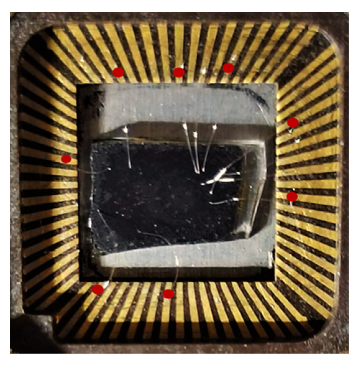
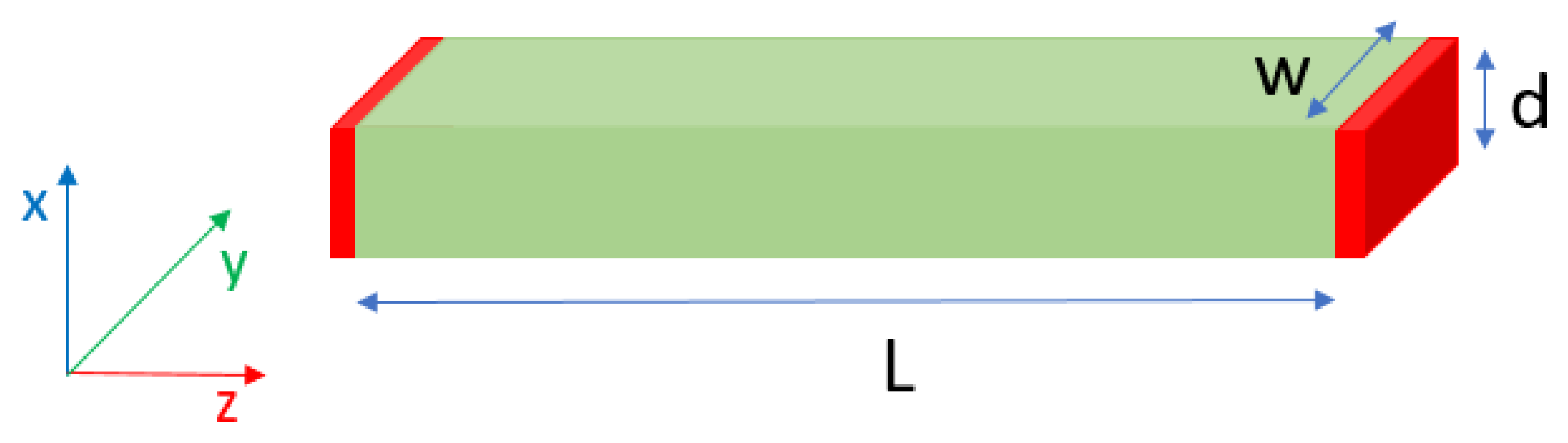
2.4. Electrical Characterization

GL and the GO materials dispersed in water (2 mg/mL), with the assistance of an ultrasound bath, were drop-casted on the substrates (glass and Si/SiO2) and allowed to dry at room temperature for about 18–24 h. The dry films were investigated by dc-transport measurements at room temperature.
The dried samples were connected to chip-holder pads using aluminum wires by a K&S 4253 wedge–wire bonder tool (Figure 1). The former technique allowed us to realize quite a similar contact area of the chip/Al wires, thus guaranteeing close contact resistance for each probed part of the film. In addition, the realization of contacts with the bonding machine ensures to replicate the measurements without interfering with the material or spoiling it. To minimize effects due to possible different film thickness, the central zone of the deposited film was characterized for each film.
Because the non-uniformity of the films could affect the quality of the electrical contact by wire bonding, a fine calibration of the bonding parameters (time, power, and force) that the tip applies on the film surface were performed. Two main checks were performed: (1) an optical wire-bond-shape inspection to assure that the wire bond linked to the film surface had a parallelepiped-like shape, thus ensuring good mechanical contact with the film; and (2) an electrical inspection by performing two and then four wire measurements to verify a negligible contact resistance, thus guaranteeing that the current could pass through the film.
The contact resistance investigation was performed by carrying out two-probe R2p and four-probe R4p dc measurements. R2p includes twice the line resistance RL, which for our setup is a few Ohms, twice the contact resistance RC, and the probed part of the film resistance RS. Because RL was several orders of magnitude smaller than the total resistance RTOT in our experiment, it became negligible. Comparing R4p and R2p, we verified that even RC is smaller than RTOT, thus leading to the conclusion that R2p~R4p. As a result, all the measurements useful in estimating the dc electrical properties of all the drop-casted films were performed in a two-probe configuration. Current–voltage (IV) measurements were carried out using a Keithley Pico-amperemeter, model 6485. The voltage was swept from −1 to 1 V by a step of 0.01 V. Measurements at a high-bias voltage were also performed up to 10 V. Current–voltage measurements were performed by probing several areas of the drop-casted films.

3. Results

3.1. Elemental Analysis

Table 1 reports the elemental composition of GL materials, together with those of the selected GO materials. The precursor of GL, CB, was also reported for comparison. The oxygen amount was evaluated by difference (due to the low amount of ashes in all of the samples, it can be assumed that the difference to 100 wt.% is attributable to oxygen).
Elemental analysis indicates that the oxygen functional groups in GL materials are not completely removed upon the chemical reduction step, leading to an oxygen content of around 40 wt.%. The high content of O after reduction is ascribable to the distinctive surface chemistry of GL materials, which is different from that typical of graphene oxide. The parent C-rich material of GL materials (CB) has short graphenic layers that undergoes massive oxidation on the edges (mainly carbonylic and carboxylic functional groups [58,60,67]), leaving the basal planes persevered (i.e., no epoxy groups or holes are present, differently from GO). As a consequence, during the reduction process, carboxylic and carbonylic groups react with hydrazine, leading to the formation of hydrazones groups with only a slight reduction in the overall oxygen content compared to the parent material, GL-ox [58]. Indeed, the presence of nitrogen is also observed in GL materials (0.5 wt.%). The O/C atomic ratio is 0.54. The oxygen content is mainly ascribed to oxygen functional groups (mainly carboxylic [60]) responsible for the stability of GL water suspension in a wide pH range (from around 3.15 to 14 [60]), located at the edges of the graphitic planes [60]. The relative percentage increment of oxygen of GO-GRA with respect to GL materials is ~20%. Both values are rather high compared to that of GO-SA.

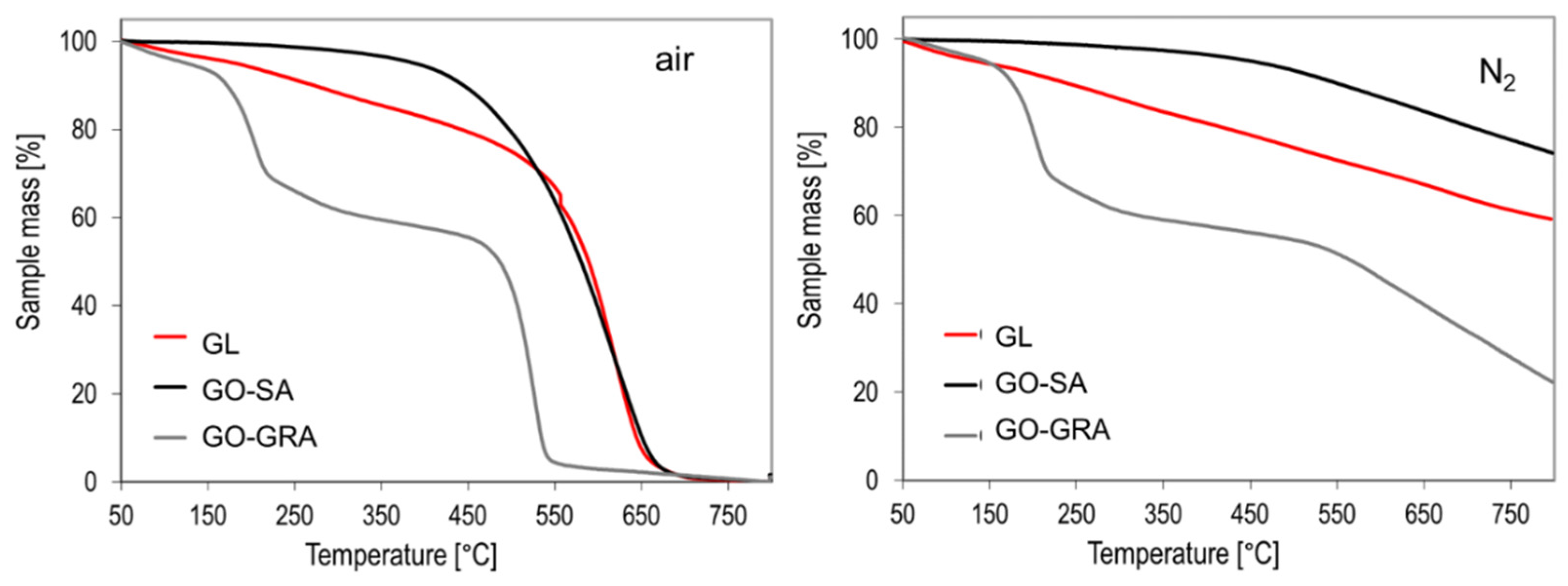
3.2. Thermal Characterization

TGA provides information about the thermal stability of GL and GO materials, as well as the number of functional groups based on their decomposition/volatilization temperature. The TGA profiles of GL materials in air and nitrogen (red line, Figure 2) exhibit a continuous weight loss (20% weight loss, ascribable to the decomposition/volatilization of oxygen-functional groups, mainly carboxylic and carbonylic). The GL burn-off occurs before 700 °C (with a maximum oxidation rate around 600 °C). The GO-SA thermal profiles do not present any marked weight loss before 350 °C, indicating a lower presence of defective sites, consistent with the lower oxygen amount in the bulk (Table 1). GL and GO-SA present a comparable bulk oxidation temperature, indicating a similar resistance toward oxidation. This circumstance reflects the presence of the low-defective basal graphitic planes [77] in both samples. The thermal profiles of GO-GRA present a marked weight loss at around 200 °C, ascribable to a huge loss in oxygen-functional groups (mainly OH, around 30 wt.%). It is noteworthy that the burn-off of GO-GRA occurs at a lower temperature (around 500 °C) with respect to GL and GO-SA materials, testifying the presence of a more defective surface, with sites easily attacked by O2 [77].

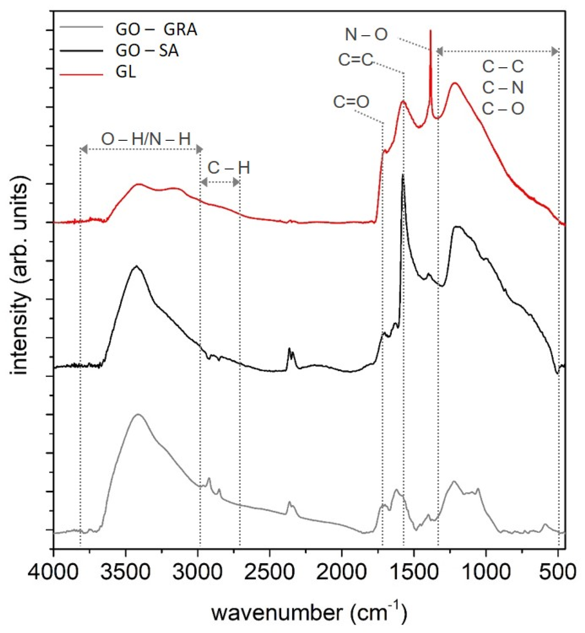
3.3. FTIR Characterization
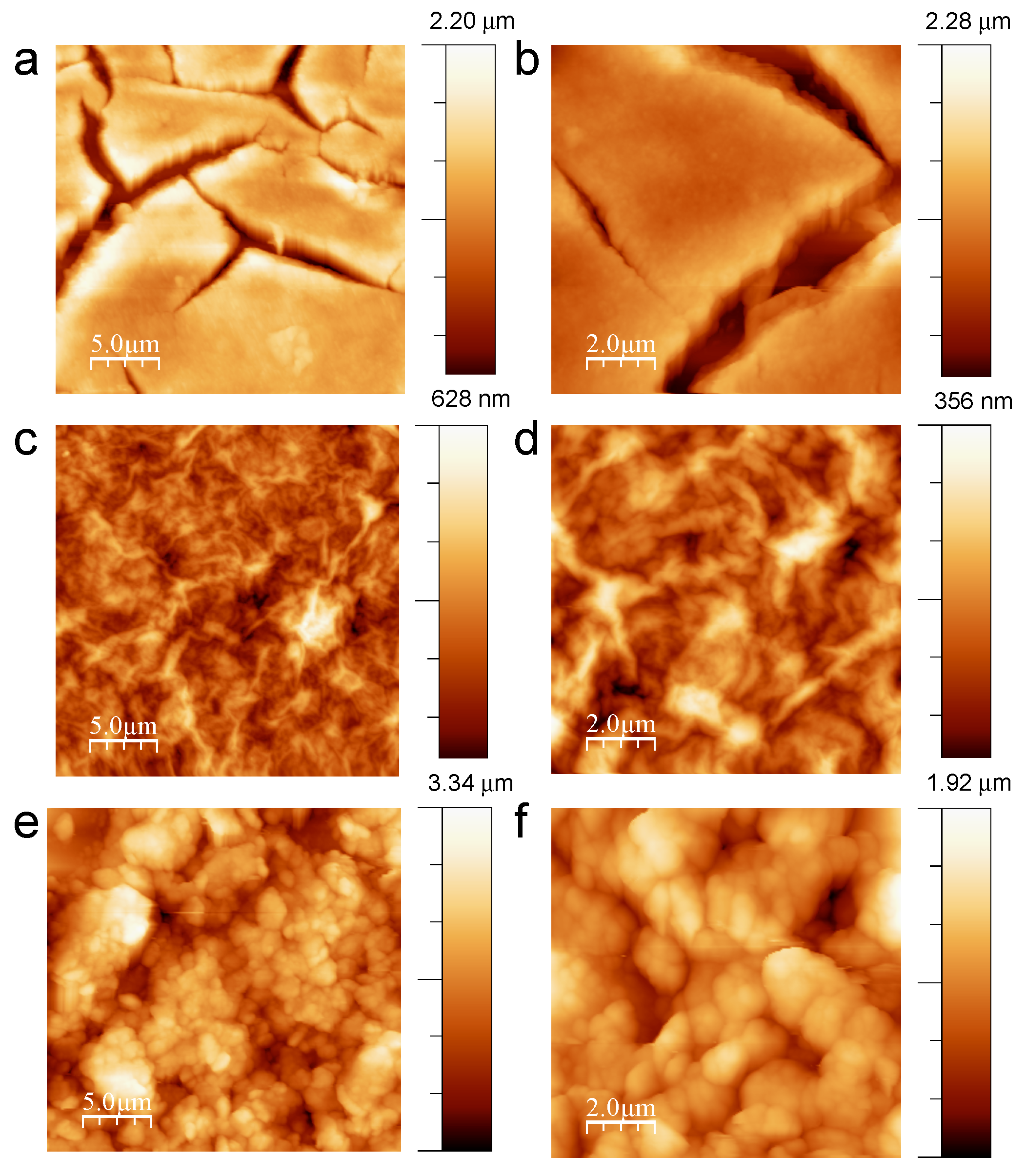
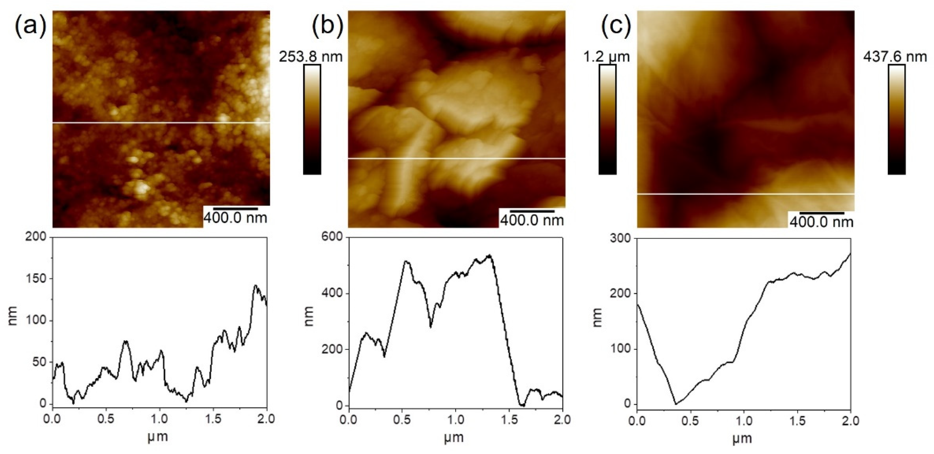
The FTIR spectra, acquired in transmittance mode in the range 450–4000 cm−1, are shown in Figure 3. The spectra are baseline-corrected and shifted for clarity. All three samples absorb similarly and are characterized by a broad shape, as typically exhibited by complex carbon networks [78].
The GL spectrum is typically poorly structured and presents a broad band in the 3000–3700 cm−1 range due to O-H stretching vibrations as a result of possibly adsorbed H2O and a broad band at 1500–1600 cm−1 due to skeletal vibrations of the sp2 graphitic domains. Moreover, the GL spectrum presents an enhanced broadband in the 1300–1100 cm−1 region, ascribable to the overlapping of multiple sp2 graphitic skeletal-stretching vibrations, and a sharp peak at 1384 cm−1 attributable to the stretching of nitrogen-containing groups (as a consequence of the strong acid top-down demolition treatment of CB by nitric acid). A weak band around 1710 cm−1, attributable to C=O stretching (residual oxygen-functional groups) [58,67,79], is also present. This last signature is negligible in the GO-SA spectrum, in agreement with the very low oxygen content; meanwhile, it is more pronounced in the case of GO-GRA. The FTIR spectrum of GO-GRA also contains bands related to alkoxy (C–O–H) and epoxy (C–O–C) groups, in addition to the bands ascribable to carbonyl (C=O), carboxyl –(COOH), and aromatic (C=C) groups [80].

3.4. AFM Imaging

The AFM images, reported in Figure 4 and Figure 5, show a good film uniformity, confirming the expected peculiar shape for all the samples. In more detail, the AFM images at a large scale (25 μm × 25 μm and 10 μm × 10 μm) of a GL film (Figure 4a,b) evidences flat terraces resulting from the good local packaging of the GL particles. This feature is driven by the GL particles self-assembling in thin film on surfaces after drying, as shown in previous reports by HRTEM and AFM [58,60], thanks to the instauration of hydrophobic interactions between the graphenic layers. The GO-SA film presents an overall granular surface, indicative of the clustering of the stacked graphitic layers (Figure 4c,d), while a flatter film is obtained from GO-GRA arising from the layering of the graphenic monolayers (Figure 4e,f).
The representative AFM image of the GL film at a higher resolution (2 μm × 2 μm, Figure 5a) evidenced the presence of clustered particles and an overall granular surface. Each particle (with an average diameter of around 40 nm [63]) stuck to one another while maintaining its individuality in a feature already known to be intrinsic to GL synthesis [67]. The GO-GRA film (Figure 5b) exhibited a surface locally organized in regions made by large, disordered, and discontinuous terraces (around 2 μm wide). Differently from the GL film, the GO-GRA surface presented a poor connection between the grains with the presence of an inter-particle-free volume, whereas the GL film appeared to be more compact. The surface of the GO-SA film (Figure 5c) looked locally smoother with better contact between the flat grains, reflecting a better self-assembly of the graphenic sheets upon drying.
The roughness, estimated as the root mean square (RMS), was about 33 nm (comparable to the particles’ average height) for the GL film; meanwhile, for the GO-SA and GO-GRA films, the RMS was 21 and 84 nm, respectively.

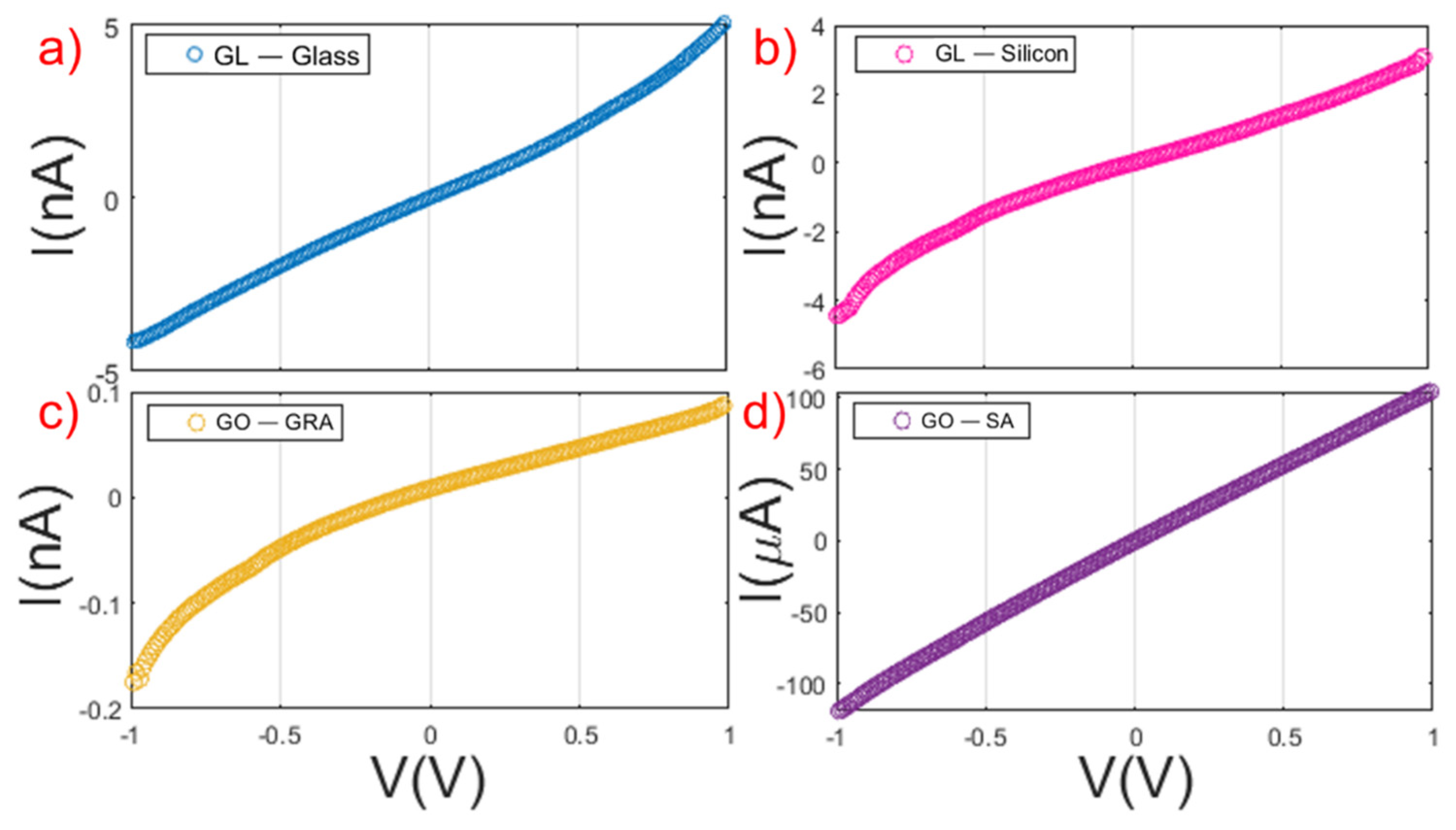
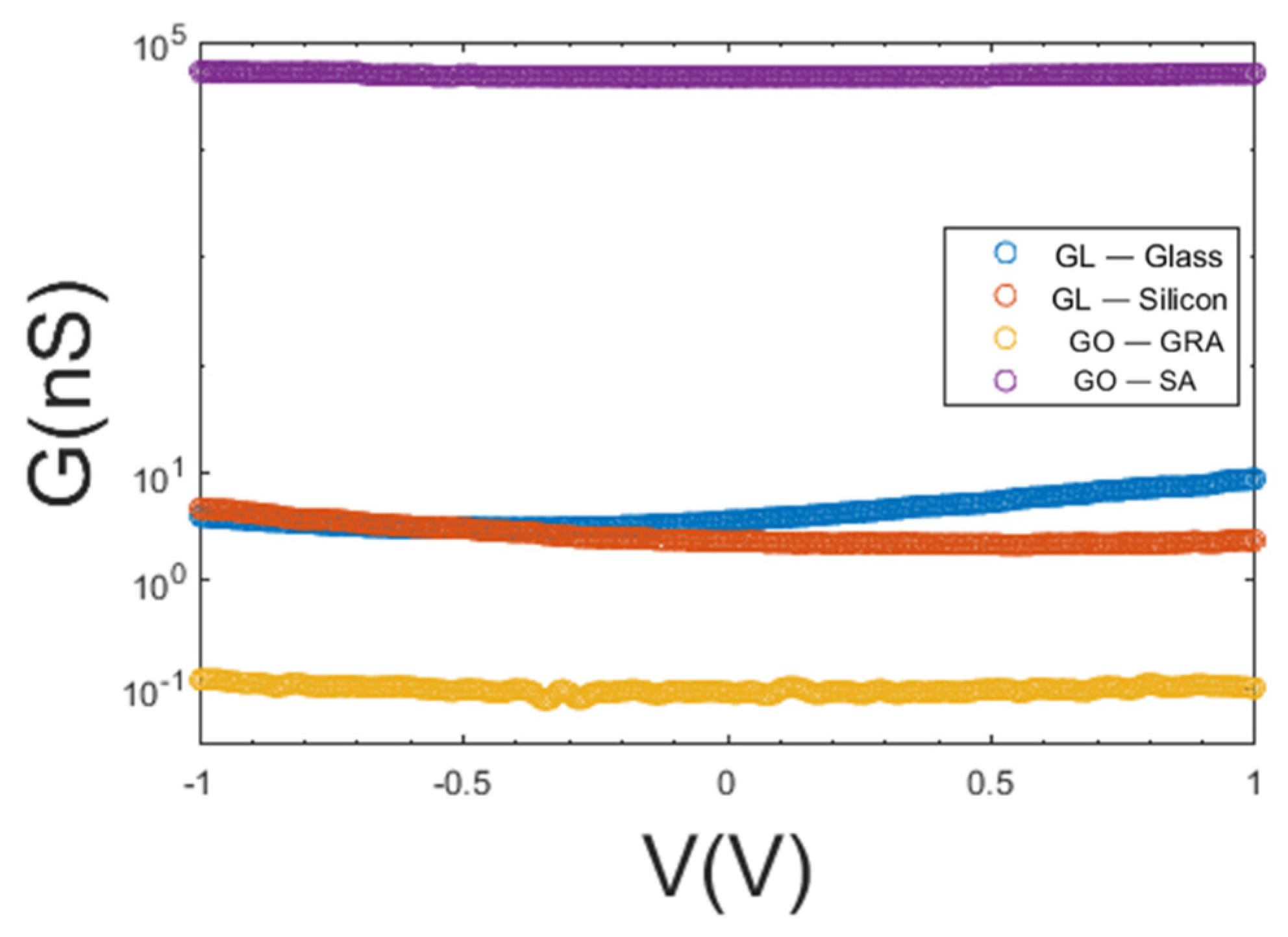
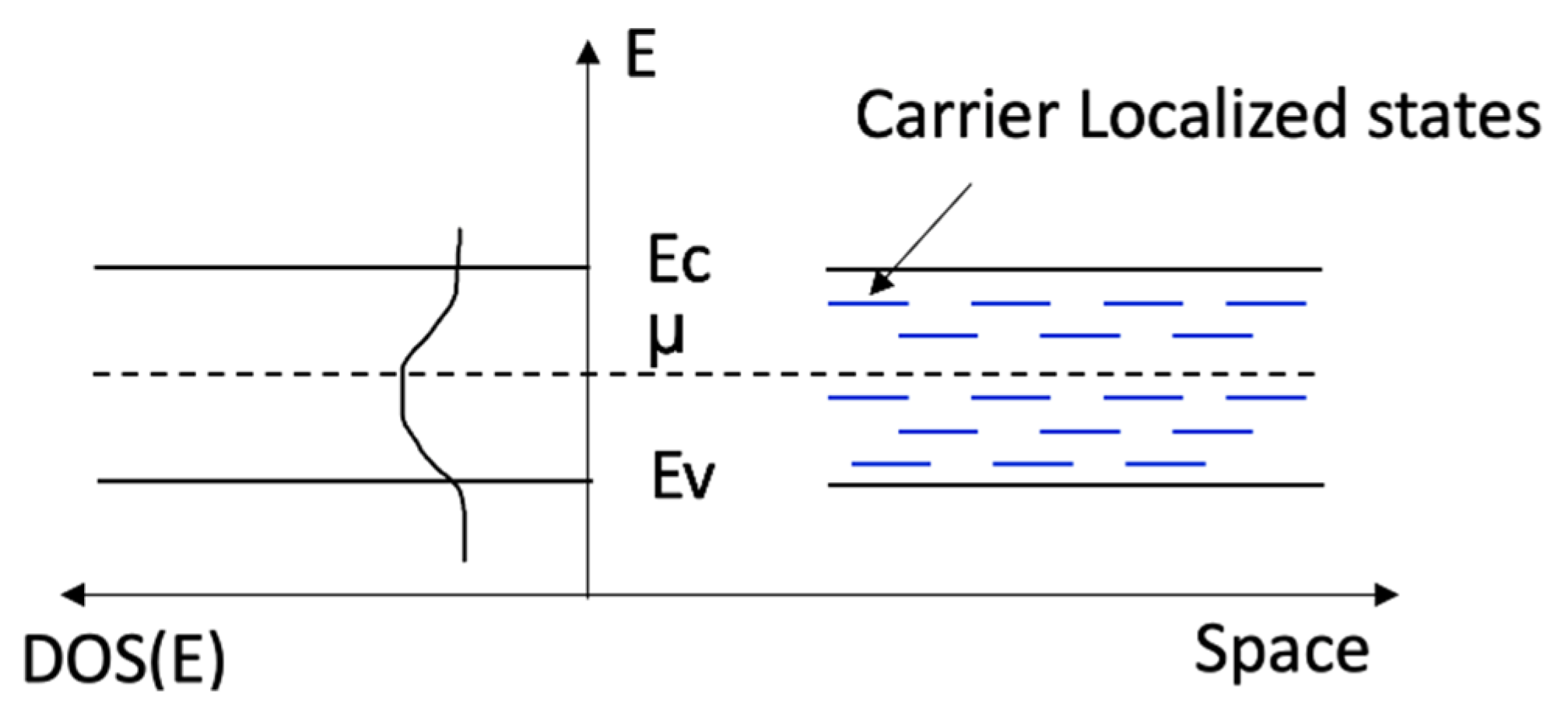
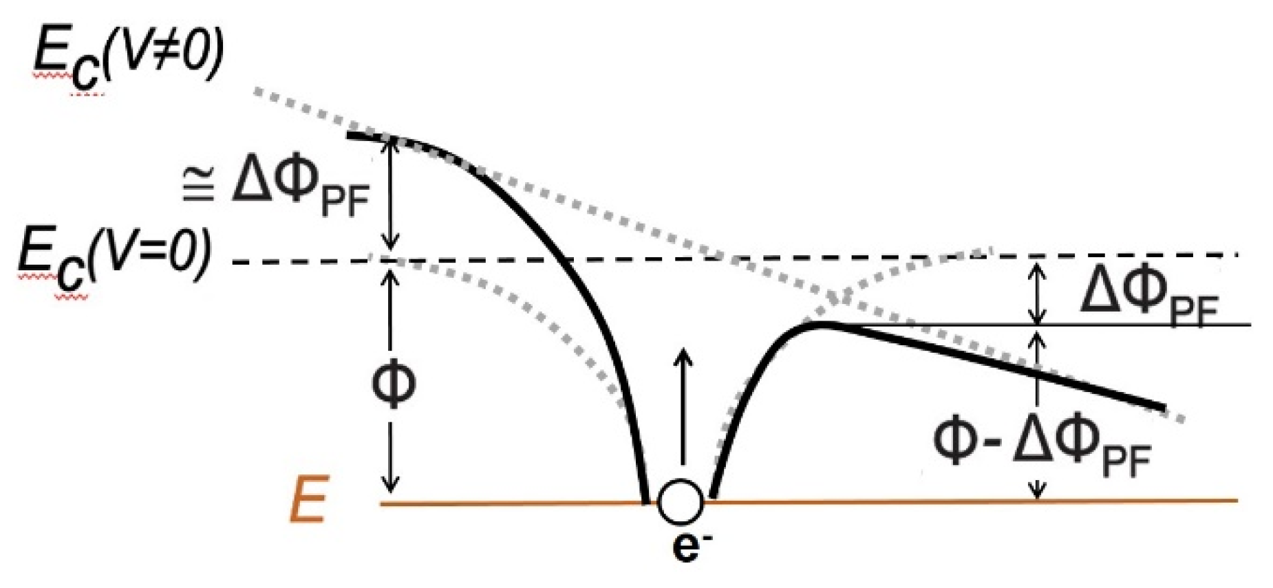
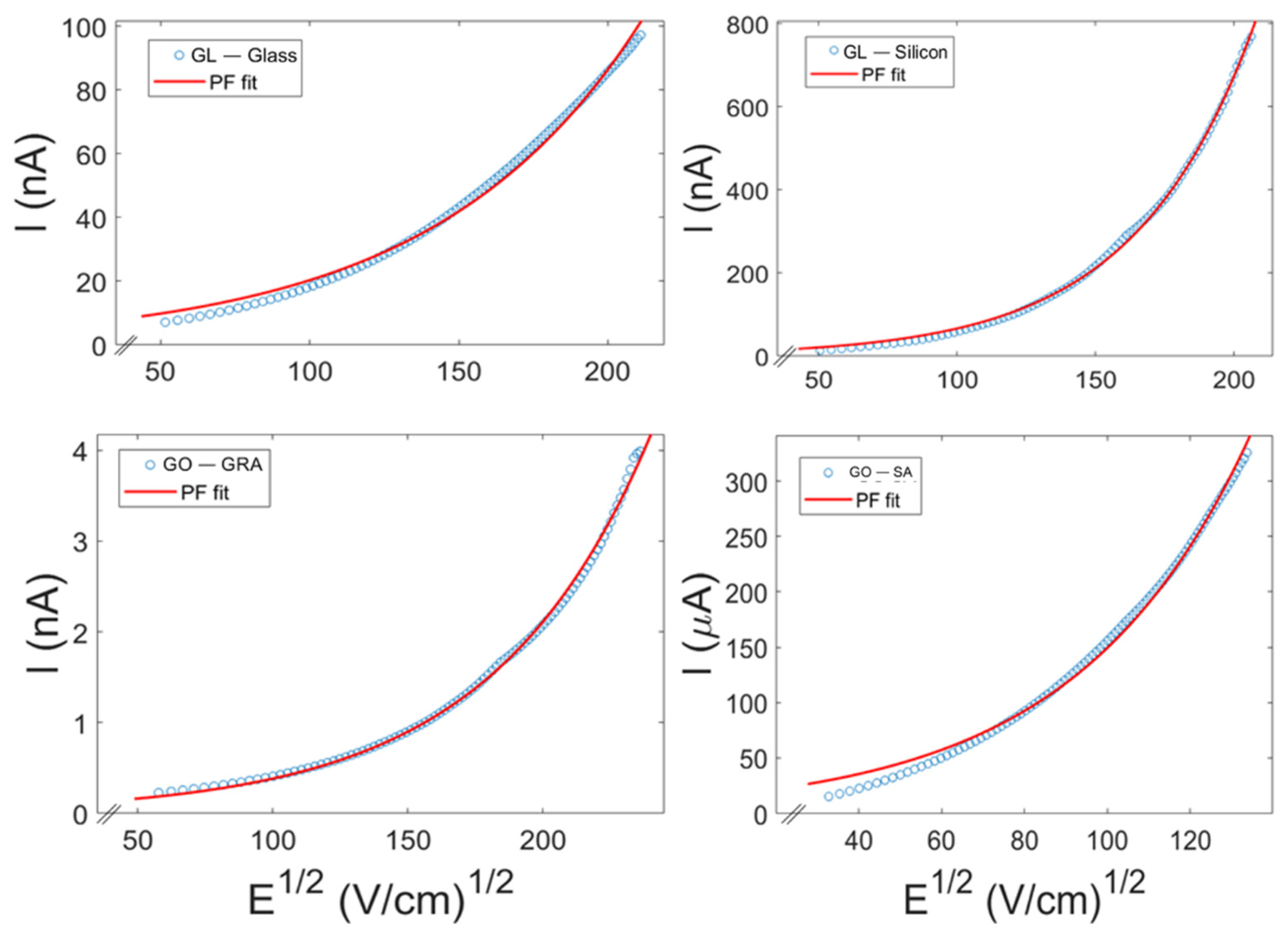
3.5. Electrical Properties

Dry GRM films showed an inhomogeneous thickness ascribable to the well-known coffee-ring phenomenon typical of the self-assembling process of GRMs. This is because of the drop-casted deposition technique that favors the formation of a ring-like film shape along the perimeter of the sample due to evaporation-induced flow [81]. The thickness of the drop-casted films was estimated by stylus-profilometer analysis. The estimated values, used to determine the dc conductivity σ, were as follows: 900 nm (GL film), 700 nm (GO-GRA film), and 3.5 µm (GO-SA film).
Several sites of the same sample were probed, and in each case, the electrical transport proprieties showed an isotropic behavior, thus confirming the homogeneity of the deposited films.
For a deep understanding of the transport properties of the GL films, a comparative analysis studying two chips made by other two benchmark materials (GO-GRA and GO-SA) was performed. The main electrical transport parameters of the characterized films are summarized in Table 2.
For all the films, the IV curves reported in Figure 6 show a common non-linear behavior typical of semiconducting materials both at room temperature and in the same bias voltage range (±1 V) [55,56]. This behavior is strongly related to the chemical characteristics of the materials described above. In fact, the oxygen amount indicates the presence of defective sites, which affect the transport mechanisms in the films [82,83]. Because of that, a current of a few nanoamperes for the GL film and of a hundred microamperes for the GO-SA film (GO-SA exhibits the presence of a smaller amount of oxygen-functional groups compared to GL materials) was measured. In addition, due to the higher oxygen content in GO-GRA, the smallest current values, a hundred picoamperes, were estimated. This behavior is in line with the electronic properties of GO estimated for different oxidation levels (25%, 50%, 75%, and 100%) by density functional calculations [84], where GO samples with a lower O content are considered to be semiconductors and GO samples with a high O content are insulating.
Differently from previous preliminary surveys on GL-based films [65,67], a strong nonlinearity of the IV curves has been highlighted, demonstrating that GL films could be used as state-of-the-art detectors based on GRMs with a high performance in terms of response.
The conductance vs. voltage (GV) curves reported in the log scale in Figure 7 have been extracted by a numerical derivative of the current–voltage (IV) measurements performed at room temperature. The GV curves of the GL film deposited on two different substrates (glass and Si/SiO2) in the range of ±1 V applied voltage showed similar values of conductance, thus indicating that no interaction occurs between the GL material and the substrates. Although a deep investigation of the role played by the substrate requires very thin deposited films (a few nanometers thick) because the typical interaction (substrate–film) length of the scale is of the order of nanometer or even less, we verified that the thickness of the deposited films is similar (both GL films are ~1 μm thick within less than 10% of the variability), as well as the electrical transport measurements.
The GV plot of the GO-SA film shows a higher conductance than the GO-GRA film. This result can again be interpreted in terms of the higher mobility of electrons due to the reduced content of oxygen in GO-SA and a consequently lower percentage of defective sites.
Deposited materials that form a disordered system usually resemble amorphous solid semiconducting materials [85]. A sketch of density of states of this kind of materials is reported in Figure 8. The observed low mobility of the characterized films implies a more complex transport model that, for high levels of applied voltage bias and no zero temperature, leads to the consideration of transport mechanisms that go beyond the aims of our analysis. For such a reason, we did not take them into account.
The electrical properties can be interpreted in the framework of the Mott–Anderson hopping-carriers-transport model [31,86,87]. This model assumes that an electron is localized in state and can be transferred to an unoccupied trap by providing thermal energy [86] or applying a bias voltage that induces a change in the shape of the potential barrier, thus decreasing its height and allowing the electron to hop to the unoccupied trap state. For amorphous, semiconducting materials (ASMs), the above-reported transport mechanism can be described by the Poole–Frenkel model [88,89,90]. This model is applicable when a carrier is trapped in a center at energy E and has to escape to the conduction level (Ec). If no voltage is applied and the system is kept at zero temperature, the trapped carrier to overcome barrier ΔΦPF needs energy that is at least equal to that of the barrier itself. Even when applying an electric field, the band bending takes hold (see Figure 9), thus creating a barrier. Because of this, the carrier requires less energy to escape the trap and to jump on the conduction band.
The former model predicts an exponential voltage-dependence of the current as reported in Equation (1). Because the GL materials are ASMs, GL film transport properties can be interpreted within this framework in accordance with the Poole–Frenkel model. We used Equation (1) [71] to evaluate the parameter β P F that allows tp distinguish the investigated graphene-related materials by the dielectric constant.
J = J 0   e x p   { 1 k B T   β P F   ( V d ) 1 / 2 }
where J 0 (=   σ 0 F) is the low field-current density, T is the absolute temperature, k B is the Boltzmann constant, V is the voltage, d is the thickness of the film, β P F is the Poole–Frenkel constant defined as β P F = ( e 3 π ϵ 0 ϵ r ) 1 / 2 , e is the electron charge, ϵ 0 is the permittivity of free space, and ϵ r is the dielectric constant [71].
Due to both the electrical contacts’ layout shown in Figure 1 and the crucial role played by the electric field in Equation (1), the geometry of the investigated sample heavily influenced its transport properties. Because of this, a deep analysis of the electrostatic properties of the sample was carried out. We schematized the device as a parallel plate capacitor, consisting of two small parallel plates with sizes w and d (sketched in red in Figure 10) separated by a material (GRM) with a length of L and a dielectric constant ϵ r (green in Figure 10).
The red conductive plates represent the bounder aluminum contacts placed on the GRM and have sizes w~30 μm and d~1 μm. The thickness of the GRM film is d, while the distance between two conductive plates (L) is of the order of millimeters. The sizes of sketched capacitor led to work in an unconventional regime (d,w << L) where the fringing electric field had to be taken in account, and it did not yield the achievement of any analytical solution [91]. In order to include the former effect in Equation (1), which allows to better define the transport properties of our samples, we approximated the investigated chips as a conventional parallel plate capacitor with a capacitance C calculated by [91] in the limit L >> d: C ( L )   C 0 π L 2 d   l n ( L d + 2 ) , where C 0 = 2 d w   ϵ 0 ϵ r   L . Because the charge is given by Q = CV and the square root of the electric field is E1/2 = ( π V d   ln ( L d + 2 ) )1/2, we can replace it in Equation (1) and proceed with the IV data fitting reported in Figure 11. This approach yielded the estimation of the values of β P F and ϵ r summarized in Table 2.
The calculated values for the selected GRMs (specifically for the GO samples) are fully comparable with those reported in the literature for similar materials [72,73,74,75,76], thus confirming the amorphous nature of the investigated samples. In addition, the obtained results show that the proposed experimental approach could represent a reliable procedure to differentiate the different materials belonging to the wide GRMs family.

4. Conclusions

Insights into the electrical characteristics of an emerging class of GRMs, namely graphene-like materials (GL), derived from a nanostructured CB, highlighted their semiconductive behavior and opened up innovative applications, such as sensing devices, bio-compatible interfaces, and inspired bio-devices (e.g., drug delivery). A careful electrical characterization at room temperature of GL films deposited from water suspensions by drop-casting onto Si/SiO2 and glass substrates has been carried out and compared with the results achieved on benchmark materials (GO samples). Transport properties have been analyzed in the framework of amorphous semiconducting materials and the data indicate a non-linear current–voltage relation for all the GRM samples. The dielectric constant of both the GL and GO samples has been extrapolated within the Frankel–Poole model and it agrees with those reported in the literature. By comparing the transport measurements of the films, no effect on the electrical properties in GL due to the interaction with the substrates has been evidenced, whereas a high resistivity for the highly oxygenated GO materials (GO-GRA), compared to the GL materials, has been observed. These results encourage a feasible use of GL films in the production of advanced materials and hybrids with practical wide-spectrum applications, ranging from electronics to optics, sensors, membranes, functional coatings, and bio-devices.

Author Contributions

Conceptualization, D.M. and M.A.; methodology, D.M., R.F., G.A., M.A.; G.P.P. and F.T.; formal analysis, R.F., V.G., M.A., G.A. and D.M.; data curation, R.F., V.G., M.A. and D.M.; writing—original draft preparation, D.M., M.A. and G.A.; writing—review and editing, all; funding acquisition, G.A. and A.P. All authors have read and agreed to the published version of the manuscript.

Funding

The research funding program of University of Naples “Federico II” (Project title: CATeGRAF, Fondo Ricerca di Ateneo—Linea B) is acknowledged for the financial support.

Institutional Review Board Statement

Not applicable.

Informed Consent Statement

Not applicable.

Data Availability Statement

Data is contained within the article.

Acknowledgments

M.A. and V.G. acknowledge the networking support by the COST Action CA19118 EsSENce, supported by the COST Association (European Cooperation in Science and Technology). D.M acknowledges Project “PON R&I 2014–2020 AIM: Attraction and International Mobility”. The authors would like to thank Loredana Parlato and Davide Massarotti for technical and scientific discussions.

Conflicts of Interest

The authors declare no conflict of interest.

References

  1. Novoselov, K.S.; Geim, A.K.; Morozov, S.V.; Jiang, D.; Zhang, Y.; Dubonos, S.V.; Grigorieva, I.V.; Firsov, A.A. Electric field effect in atomically thin carbon films. Science 2004, 306, 666–669. [Google Scholar] [CrossRef] [PubMed] [Green Version]
  2. Berger, C.; Song, Z.M.; Li, X.B.; Wu, X.S.; Brown, N.; Naud, C.; Mayo, D.; Li, T.B.; Hass, J.; Marchenkov, A.N.; et al. Electronic confinement and coherence in patterned epitaxial graphene. Science 2006, 312, 1191–1196. [Google Scholar] [CrossRef] [PubMed] [Green Version]
  3. Geim, A.K.; Novoselov, K.S. The rise of graphene. Nat. Mater. 2007, 6, 183–191. [Google Scholar] [CrossRef] [PubMed]
  4. He, H.; Kim, K.H.; Danilov, A.; Montemurro, D.; Yu, L.; Park, Y.W.; Lombardi, F.; Bauch, T.; Moth-Poulsen, K.; Iakimov, T.; et al. Uniform doping of graphene close to the Dirac point by polymer-assisted assembly of molecular dopants. Nat. Commun. 2018, 9, 3956. [Google Scholar] [CrossRef] [PubMed] [Green Version]
  5. Avouris, P. Graphene: Electronic and Photonic Properties and Devices. Nano Lett. 2010, 10, 4285–4294. [Google Scholar] [CrossRef] [PubMed]
  6. Liu, N.; Fu, L.; Dai, B.; Yan, K.; Liu, X.; Zhao, R.; Zhang, Y.; Liu, Z. Universal Segregation Growth Approach to Wafer-Size Graphene from Non-Noble Metals. Nano Lett. 2011, 11, 297–303. [Google Scholar] [CrossRef] [PubMed]
  7. Papageorgiou, D.G.; Kinloch, I.A.; Young, R.J. Mechanical properties of graphene and graphene-based nanocomposites. Prog. Mater. Sci. 2017, 90, 75–127. [Google Scholar] [CrossRef]
  8. Yue, S.; Zhou, H.; Geng, D.; Sun, Z.; Arita, M.; Shimada, K.; Cheng, P.; Chen, L.; Meng, S.; Wu, K.; et al. Experimental observation of Dirac cones in artificial graphene lattices. Phys. Rev. B 2020, 102, 201401. [Google Scholar] [CrossRef]
  9. Heersche, H.B.; Jarillo-Herrero, P.; Oostinga, J.B.; Vandersypen, L.M.K.; Morpurgo, A.F. Bipolar supercurrent in graphene. Nature 2007, 446, 56–59. [Google Scholar] [CrossRef] [PubMed] [Green Version]
  10. Chung, C.; Kim, Y.-K.; Shin, D.; Ryoo, S.-R.; Hong, B.H.; Min, D.-H. Biomedical Applications of Graphene and Graphene Oxide. Acc. Chem. Res. 2013, 46, 2211–2224. [Google Scholar] [CrossRef] [PubMed]
  11. Rao, C.N.R.; Biswas, K.; Subrahmanyam, K.S.; Govindaraj, A. Graphene, the new nanocarbon. J. Mater. Chem. 2009, 19, 2457–2469. [Google Scholar] [CrossRef]
  12. Abergel, D.S.L.; Apalkov, V.; Berashevich, J.; Ziegler, K.; Chakraborty, T. Properties of graphene: A theoretical perspective. Adv. Phys. 2010, 59, 261–482. [Google Scholar] [CrossRef] [Green Version]
  13. Emtsev, K.V.; Bostwick, A.; Horn, K.; Jobst, J.; Kellogg, G.L.; Ley, L.; McChesney, J.L.; Ohta, T.; Reshanov, S.A.; Rohrl, J.; et al. Towards wafer-size graphene layers by atmospheric pressure graphitization of silicon carbide. Nat. Mater. 2009, 8, 203–207. [Google Scholar] [CrossRef] [PubMed] [Green Version]
  14. Li, X.S.; Cai, W.W.; An, J.H.; Kim, S.; Nah, J.; Yang, D.X.; Piner, R.; Velamakanni, A.; Jung, I.; Tutuc, E.; et al. Large-area synthesis of high-quality and uniform graphene films on copper foils. Science 2009, 324, 1312–1314. [Google Scholar] [CrossRef] [PubMed] [Green Version]
  15. Lee, S.; Lee, K.; Zhong, Z. Wafer Scale Homogeneous Bilayer Graphene Films by Chemical Vapor Deposition. Nano Lett. 2010, 10, 4702–4707. [Google Scholar] [CrossRef] [PubMed] [Green Version]
  16. Lee, Y.; Bae, S.; Jang, H.; Jang, S.; Zhu, S.-E.; Sim, S.H.; Song, Y.I.; Hong, B.H.; Ahn, J.-H. Wafer-Scale Synthesis and Transfer of Graphene Films. Nano Lett. 2010, 10, 490–493. [Google Scholar] [CrossRef] [Green Version]
  17. Gao, L.; Ni, G.-X.; Liu, Y.; Liu, B.; Castro Neto, A.H.; Ping Loh, K.P. Face-to-face transfer of wafer-scale graphene films. Nature 2014, 505, 190–194. [Google Scholar] [CrossRef] [PubMed]
  18. Gong, Y.; Zhang, X.; Liu, G.; Wu, L.; Geng, X.; Long, M.; Cao, X.; Guo, Y.; Li, W.; Xu, J.; et al. Layer-Controlled and Wafer-Scale Synthesis of Uniform and High-Quality Graphene Films on a Polycrystalline Nickel Catalyst. Adv. Funct. Mater. 2012, 22, 3153–3159. [Google Scholar] [CrossRef]
  19. Arcadio, F.; Zeni, L.; Montemurro, D.; Eramo, C.; Di Ronza, S.; Perri, C.; D’Agostino, G.; Chiaretti, G.; Porto, G.; Cennamo, N. Biochemical sensing exploiting plasmonic sensors based on gold nanogratings and polymer optical fibers. Photonics Res. 2021, 9, 1397–1408. [Google Scholar] [CrossRef]
  20. Vettoliere, A.; Satariano, R.; Ferraiuolo, R.; Di Palma, L.; Ahmad, H.G.; Ausanio, G.; Pepe, G.P.; Tafuri, F.; Montemurro, D.; Granata, C.; et al. Aluminum-ferromagnetic Josephson tunnel junctions for high quality magnetic switching devices. Appl. Phys. Lett. 2022, 120, 262601. [Google Scholar] [CrossRef]
  21. Zito, G.; Rusciano, G.; Pesce, G.; Malafronte, A.; Rocco Di Girolamo, R.; Ausanio, G.; Vecchione, A.; Sasso, A. Nanoscale engineering of two-dimensional disordered hyperuniform block-copolymer assemblies. Phys. Rev. E 2015, 92, 050601(R). [Google Scholar] [CrossRef] [PubMed]
  22. Trabaldo, E.; Ruffieux, S.; Andersson, E.; Arpaia, R.; Montemurro, D.; Schneiderman, J.F.; Kalaboukhov, A.; Winkler, D.; Lombardi, F.; Bauch, T. Properties of grooved Dayem bridge based YBa2Cu3O7−𝜹 superconducting quantum interference devices and magnetometers. Appl. Phys. Lett. 2020, 116, 132601. [Google Scholar] [CrossRef] [Green Version]
  23. Mahashabde, S.; Otto, E.; Montemurro, D.; de Graaf, S.; Kubatkin, S.; Danilov, A. Fast Tunable High-Q-Factor Superconducting Microwave Resonators. Phys. Rev. Appl. 2020, 14, 044040. [Google Scholar] [CrossRef]
  24. Baghdadi, R.; Arpaia, R.; Stepantsov, E.; Arzeo, M.; Golubev, D.; Montemurro, D.; Andersson, E.; Bauch, T.; Lombardi, F. Study of in-plane electrical transport anisotropy of a-axis oriented YBa2Cu3O7−δ nanodevices. Phys. Rev. B 2017, 95, 184505. [Google Scholar] [CrossRef] [Green Version]
  25. Park, H.-Y.; Jung, W.-S.; Kang, D.-H.; Jeon, J.; Yoo, G.; Park, Y.; Lee, J.; Jang, Y.H.; Lee, J.; Park, S.; et al. Extremely Low Contact Resistance on Graphene through n-Type Doping and Edge Contact Design Advanced. Materials 2016, 28, 864–870. [Google Scholar]
  26. Lee, E.J.H.; Balasubramanian, K.; Weitz, R.T.; Burghard, M.; Kern, K. Contact and edge effects in graphene devices. Nat. Nanotechnol. 2008, 3, 486–490. [Google Scholar] [CrossRef] [PubMed]
  27. Cusati, T.; Fiori, G.; Gahoi, A.; Passi, V.; Lemme, M.C.; Fortunelli, A.; Iannaccone, G. Electrical properties of graphene-metal contacts. Sci. Rep. 2017, 7, 5109. [Google Scholar] [CrossRef] [PubMed] [Green Version]
  28. Kunakova, G.; Surendran, A.P.; Montemurro, D.; Salvato, M.; Golubev, D.; Andzane, J.; Erts, D.; Bauch, T.; Lombardi, F. Topological insulator nanoribbon Josephson junctions: Evidence for size effects in transport properties. J. Appl. Phys. 2020, 128, 194304. [Google Scholar] [CrossRef]
  29. Montemurro, D.; Stornaiuolo, D.; Massarotti, D.; Ercolani, D.; Sorba, L.; Beltram, F.; Tafuri, F.; Roddaro, S. Suspended InAs nanowire Josephson junctions assembled via dielectrophoresis. Nanotechnology 2015, 26, 385302. [Google Scholar] [CrossRef] [PubMed] [Green Version]
  30. Trabaldo, E.; Pfeiffer, C.; Andersson, E.; Leonidovich, M.C.; Arpaia, R.; Montemurro, D. SQUID magnetometer based on Grooved Dayem nanobridges and a flux transformer. IEEE Trans. Appl. Supercond. 2020, 30, 9126148. [Google Scholar] [CrossRef]
  31. Montemurro, D.; Massarotti, D.; Lucignano, P.; Roddaro, S.; Stornaiuolo, D.; Ercolani, D.; Sorba, L.; Tagliacozzo, A.; Beltram, F.; Tafuri, F. Towards a Hybrid High Critical Temperature Superconductor Junction with a Semiconducting InAs Nanowire Barrier. J. Supercond. Nov. Magn. 2015, 28, 3429–3437. [Google Scholar] [CrossRef]
  32. Satariano, R.; Parlato, L.; Vettoliere, A.; Caruso, R.; Ahmad, H.G.; Miano, A.; Di Palma, L.; Daniela Salvoni, D.; Montemurro, D.; Granata, C.; et al. Inverse magnetic hysteresis of the Josephson supercurrent: Study of the magnetic properties of thin niobium/permalloy (Fe20Ni80) interfaces. Phys. Rev. B 2021, 103, 224521. [Google Scholar] [CrossRef]
  33. Thilgen, C.; Diederich, F. Structural Aspects of Fullerene Chemistry. A Journey through Fullerene Chirality. Chem. Rev. 2006, 106, 5049–5135. [Google Scholar] [CrossRef]
  34. Mittal, G.; Dhand, V.; Rhee, K.Y.; Park, S.-J.; Lee, W.R. A review on carbon nanotubes and graphene as fillers in reinforced polymer nanocomposites. J. Ind. Eng. Chem. 2015, 21, 11–25. [Google Scholar] [CrossRef]
  35. Chen, W.; Yan, L.; Bangal, P.R. Chemical Reduction of Graphene Oxide to Graphene by Sulfur-Containing Compounds. J. Phys. Chem. C 2010, 114, 19885–19890. [Google Scholar] [CrossRef]
  36. Eigler, S.; Grimm, S.; Enzelberger-Heim, M.; Müller, P.; Hirsc, A. Graphene oxide: Efficiency of reducing agents. Chem. Commun. 2013, 49, 7391–7793. [Google Scholar] [CrossRef] [Green Version]
  37. Bhuyan, S.A.; Nizam Uddin, N.; Islam, M.; Bipasha, F.A.; Hossain, S.S. Synthesis of graphene. Int. Nano Lett. 2016, 6, 65–83. [Google Scholar] [CrossRef] [Green Version]
  38. McEuen, P.L. Carbon-based electronics. Nature 1998, 393, 15–17. [Google Scholar] [CrossRef]
  39. Cha, C.; Shin, S.R.; Annabi, N.; Dokmeci, M.R.; Khademhossein, A. Carbon-Based Nanomaterials: Multifunctional Materials for Biomedical Engineering. ACS Nano 2013, 7, 2891–2897. [Google Scholar] [CrossRef]
  40. Compton, O.C.; Nguyen, S.T. Graphene Oxide, Highly Reduced Graphene Oxide, and Graphene: Versatile Building Blocks for Carbon-Based Materials. Small 2010, 6, 711–723. [Google Scholar] [CrossRef]
  41. Bonavolontà, C.; Camerlingo, C.; Carotenuto, G.; De Nicola, S.; Longo, A.; Meola, C.; Boccardi, S.; Palomba, M.; Pepe, G.P.; Valentino, M. Characterization of piezoresistive properties of graphene-supported polymer coating for strain sensor applications. Sens. Actuators A Physical. 2016, 252, 26–34. [Google Scholar] [CrossRef]
  42. Georgakilas, V.; Perman, J.A.; Tucek, J.; Zboril, R. Broad Family of Carbon Nanoallotropes: Classification, Chemistry, and Applications of Fullerenes, Carbon Dots, Nanotubes, Graphene, Nanodiamonds, and Combined Superstructures. Chem. Rev. 2015, 115, 4744–4822. [Google Scholar] [CrossRef] [PubMed]
  43. Poorna, A.R.; Saravanathamizhan, R.; Balasubramanian, N. Graphene and graphene-like structure from biomass for Electrochemical Energy Storage application—A Review. Electrochem. Sci. Adv. 2021, 1, e2000028. [Google Scholar] [CrossRef]
  44. Safian, M.T.U.; Haron, U.S.; Ibrahim, M.M. A review on bio-based graphene derived from biomass wastes. BioResources 2020, 15, 9756. [Google Scholar] [CrossRef]
  45. Rabia, I.; Jan, B.M.; Ahmad, W. Advances in synthesis of graphene derivatives using industrial wastes precursors; prospects and challenges. J. Mater. Res. Technol. 2020, 9, 15924–15951. [Google Scholar]
  46. Octavia, V.; Ribeiro, R.S.; Diaz de Tuesta, J.L.; Gomes, H.T.; Silva, A.M.T. A systematic literature review on the conversion of plastic wastes into valuable 2D graphene-based materials. Chem. Eng. J. 2022, 428, 131399. [Google Scholar]
  47. Tang, Q.; Zhou, Z.; Chen, Z. Graphene-related nanomaterials: Tuning properties by functionalization. Nanoscale 2013, 5, 4541–4583. [Google Scholar] [CrossRef] [PubMed]
  48. Chavez-Valdez, A.; Shaffer, M.S.P.; Boccaccini, A.R. Applications of Graphene Electrophoretic Deposition. A Review. J. Phys. Chem. B 2013, 117, 1502–1515. [Google Scholar] [CrossRef] [PubMed]
  49. Mas-Ballesté, R.; Gómez-Navarro, C.; Gómez-Herrero, J.; Zamora, F. 2D materials: To graphene and beyond. Nanoscale 2011, 3, 20–30. [Google Scholar] [CrossRef]
  50. Krueger, M.; Berg, S.; Stone, D.A.; Strelcov, E.; Dikin, D.A.; Kim, J.; Cote, L.J.; Huang, J.; Kolmakov, A. Drop-Casted Self-Assembling Graphene Oxide Membranes for Scanning Electron Microscopy on Wet and Dense Gaseous Samples. ACS Nano 2011, 5, 10047–10054. [Google Scholar] [CrossRef]
  51. Gomez-Navarro, C.; Weitz, R.T.; Bittner, A.M.; Scolari, M.; Mews, A.; Burghard, M.; Kern, K. Electronic Transport Properties of Individual Chemically Reduced Graphene Oxide Sheets. Nano Lett. 2007, 7, 3499. [Google Scholar] [CrossRef] [PubMed]
  52. Khabibrakhmanov, A.I.; Sorokin, P.B. Electronic properties of graphene oxide: Nanoroads towards novel applications. Nanoscale 2022, 14, 4131–4144. [Google Scholar] [CrossRef] [PubMed]
  53. Venugopal, G.; Krishnamoorthy, K.; Mohan, R.; Kim, S.-J. An investigation of the electrical transport properties of graphene-oxide thin films. Mater. Chem. Phys. 2012, 132, 29–33. [Google Scholar] [CrossRef]
  54. Casero, E.; Parra-Alfambra, A.M.; Petit-Domínguez, M.D.; Pariente, F.; Lorenzo, E.; Alonso, C. Differentiation between graphene oxide and reduced graphene by electrochemical impedance spectroscopy (EIS). Electrochem. commun. 2012, 20, 63–66. [Google Scholar] [CrossRef]
  55. Zhuge, F.; Hu, B.; He, C.; Zhou, X.; Liu, Z.; Li, R.-W. Mechanism of nonvolatile resistive switching in graphene oxide thin films. Carbon 2011, 49, 3796–3802. [Google Scholar] [CrossRef]
  56. Wu, X.; Sprinkle, M.; Li, X.; Ming, F.; Berger, C.; de Heer, W.A. Epitaxial-Graphene/Graphene-Oxide Junction: An Essential Step towards Epitaxial Graphene Electronics. Phys. Rev. Lett. 2008, 101, 026801. [Google Scholar] [CrossRef] [Green Version]
  57. Kim, T.W.; Gao, Y.; Acton, O.; Yip, H.L.; Ma, H.; Chen, H.; Jen, A.K.Y. Graphene oxide nanosheets based organic field effect transistor for nonvolatile memory applications. Appl. Phys. Lett. 2010, 97, 023310. [Google Scholar] [CrossRef]
  58. Alfè, M.; Gargiulo, V.; Di Capua, R.; Chiarella, F.; Rouzaud, J.N.; Vergara, A.; Ciajolo, A. Wet Chemical Method for Making Graphene-like Films from Carbon Black. ACS Appl. Mater. Interfaces 2012, 4, 4491–4498. [Google Scholar] [CrossRef] [Green Version]
  59. Alfè, M.; Spasiano, D.; Gargiulo, V.; Vitiello, G.; Di Capua, R.; Marotta, R. TiO2/graphene-like photocatalysts for selective oxidation of 3-pyridine-methanol to vitamin B3 under UV/solar simulated radiation in aqueous solution at room conditions: The effect of morphology on catalyst performances. Appl. Catal. A Gen 2014, 487, 91–99. [Google Scholar] [CrossRef]
  60. Alfè, M.; Gargiulo, V.; Di Capua, R. Tuning the surface morphology of self-assembled graphene-like thin films through pH variation. Appl. Surf. Sci. 2015, 353, 628–635. [Google Scholar] [CrossRef]
  61. Papari, G.P.; Gargiulo, V.; Alfè, M.; Di Capua, R.; Pezzella, A.; Andreone, A. THz spectroscopy on graphene-like materials for bio-compatible devices. J. Appl. Phys. 2017, 121, 145107. [Google Scholar] [CrossRef]
  62. Olivi, M.; Alfè, M.; Gargiulo, V.; Valle, F.; Mura, F.; Di Giosia, M.; Rapino, S.; Palleschi, C.; Uccelletti, D.; Fiorito, S. Antimicrobial properties of graphene-like nanoparticles: Coating effect on Staphylococcus aureus. J. Nanopart. Res. 2016, 18, 358. [Google Scholar] [CrossRef]
  63. D’Amora, M.; Alfe, M.; Gargiulo, V.; Silvia Giordani, S. Graphene-Like Layers from Carbon Black: In Vivo Toxicity Assessment. Nanomaterials 2020, 10, 1472. [Google Scholar] [CrossRef] [PubMed]
  64. Alfe, M.; Minopoli, G.; Tartaglia, M.; Gargiulo, V.; Caruso, U.; Pepe, G.P.; Ausanio, G. Coating of flexible PDMS substrates through Matrix-Assisted Pulsed Laser Evaporation (MAPLE) with a new-concept biocompatible graphenic material. Nanomaterials 2022, 12, 3663. [Google Scholar] [CrossRef]
  65. Gargiulo, V.; Alfè, M.; Di Capua, R.; Togna, A.R.; Cammisotto, V.; Fiorito, S.; Musto, A.; Navarra, A.; Parisi, S.; Pezzella, A. Supplementing π-Systems: Eumelanin and Graphene-Like Integration Towards High Conductive Material for Mammalian Cell Culture Bio-interface. J. Mater. Chem. B 2015, 3, 5070–5079. [Google Scholar] [CrossRef] [PubMed]
  66. Di Capua, R.; Gargiulo, V.; Alfè, M.; De Luca, G.M.; Skála, T.; Mali, G.; Pezzella, A. Eumelanin Graphene-Like Integration: The Impact on Physical Properties and Electrical Conductivity. Front. Chem. 2019, 7, 121. [Google Scholar] [CrossRef] [PubMed] [Green Version]
  67. Gargiulo, V.; Alfano, B.; Di Capua, R.; Alfè, M.; Vorokhta, M.; Polichetti, T.; Massera, E.; Miglietta, M.L.; Schiattarella, C.; Di Francia, G. Graphene-like layers as promising chemiresistive sensing material for detection of alcohols at low concentration. J. Appl. Phys. 2018, 123, 024503. [Google Scholar] [CrossRef]
  68. Villani, F.; Loffredo, F.; Alfano, B.; Miglietta, M.L.; Verdoliva, L.; Alfè, M.; Gargiulo, V.; Polichetti, T. Graphene-Like Based-Chemiresistors Inkjet-Printed onto Paper Substrate. In Sensors: Lecture Notes in Electrical Engineering; Andò, B., Baldini, F., Di Natale, C., Ferrari, V., Marletta, V., Marrazza, G., Militello, V., Miolo, G., Rossi, M., Scalise, L., et al., Eds.; Springer International Publishing: Cham, Switzerland, 2019; Volume 539, pp. 337–343. [Google Scholar]
  69. Yao, Y.; Chen, X.; Zhu, J.; Zeng, B.; Wu, Z.; Li, X. The effect of ambient humidity on the electrical properties of graphene oxide films. Nanoscale Res. Lett. 2012, 7, 363. [Google Scholar] [CrossRef] [Green Version]
  70. Travlou, N.A.; Singh, K.; Rodríguez-Castellón, E.; Bandosz, T.J. Cu–BTC MOF–graphene-based hybrid materials as low concentration ammonia sensors. J. Mater. Chem. A 2015, 3, 11417–11429. [Google Scholar] [CrossRef]
  71. Mahrous, S.; Hanfy, T.A. Poole–Frenkel conduction in polyvinyl chloride stabilized with dibutylin laurate–maleate. Curr. Appl. Phys. 2004, 4, 461–464. [Google Scholar] [CrossRef]
  72. Santos, E.J.G.; Kaxiras, E. Electric-field dependence of the effective dielectric constant in graphene. Nano Lett. 2013, 13, 898–902. [Google Scholar] [CrossRef]
  73. Reed, J.P.; Uchoa, B.; Joe, Y.I.; Gan, Y.; Casa, D.; Fradkin, E.; Abbamonte, P. The Effective Fine-Structure Constant of Freestanding Graphene Measured in Graphite. Science 2010, 330, 805–808. [Google Scholar] [CrossRef] [Green Version]
  74. Wang, Y.; Brar, V.W.; Shytov, A.V.; Wu, Q.; Regan, W.; Tsai, H.Z.; Zettl, A.; Levitov, L.S.; Crommie, M.F. Mapping Dirac quasiparticles near a single Coulomb impurity on graphene. Nat. Phys. 2012, 8, 653–657. [Google Scholar] [CrossRef]
  75. Hwang, C.; Siegel, D.A.; Mo, S.-K.; Regan, W.; Ismach, A.; Zhang, Y.; Zettl, A.; Lanzara, A. Fermi velocity engineering in graphene by substrate modification. Sci. Rep. 2012, 2, 590. [Google Scholar] [CrossRef] [Green Version]
  76. Bostwick, A.; Speck, F.; Seyller, T.; Horn, K.; Polini, M.; Asgari, R.; MacDonald, A.H.; Rotenberg, E. Observation of Plasmarons in Quasi-Freestanding Doped Graphene. Science 2010, 328, 999–1002. [Google Scholar] [CrossRef]
  77. Farivar, F.; Yap, P.L.; Hassan, K.; Tung, T.T.; Tran, D.N.H.; Pollard, A.J.; Losic, D. Unlocking thermogravimetric analysis (TGA) in the fight against “Fake graphene” materials. Carbon 2021, 179, 505–513. [Google Scholar] [CrossRef]
  78. Arnal, C.; Alfè, M.; Gargiulo, V.; Ciajolo, A.; Alzueta, M.U.; Millera, A.; Bilbao, R. Characterization of soot. In Cleaner Combustion: Green Energy and Technology, 1st ed.; Battin-Leclerc, F., Simmie, J., Blurock, E., Eds.; Springer: London, UK, 2003; pp. 333–362. [Google Scholar]
  79. Silverstein, R.M.; Webster, F.X.; Kiemle, D.J. Spectrometric Identification of Organic Compounds, 4th ed.; Wiley: Hoboken, NJ, USA, 2008. [Google Scholar]
  80. Al-Gaashani, R.; Najjar, A.; Zakari, Y.; Mansour, S.; Atieh, M.A. XPS and structural studies of high-quality graphene oxide and reduced graphene oxide prepared by different chemical oxidation methods. Ceram. Int. 2019, 45, 14439–14448. [Google Scholar] [CrossRef]
  81. Nayak, L.; Mohanty, S.; Nayak, S.K.; Ramadoss, A. A review on inkjet printing of nanoparticle inks for flexible electronics. J. Mater. Chem. C 2019, 7, 8771–8795. [Google Scholar] [CrossRef]
  82. Jastrzebska, M.M.; Isotalo, H.; Paloheimo, J.; Stubb, H. Electrical conductivity of synthetic DOPA-melanin polymer for different hydration states and temperatures. J. Biomater. Sci. Polym. Ed. 1995, 7, 577–586. [Google Scholar] [CrossRef]
  83. Liu, W.; Speranza, G. Tuning the Oxygen Content of Reduced Graphene Oxide and Effects on Its Properties. ACS Omega 2021, 6, 6195–6205. [Google Scholar] [CrossRef]
  84. Vacacela Gomez, C.; Robalino, E.; Haro, D.; Tene, T.; Escudero, P.; Haro, A.; Orbe, J. Structural and electronic properties of graphene oxide for different degree of oxidation. Mater. Today: Proc. 2016, 3, 796–802. [Google Scholar]
  85. Adler, D. Amorphous-Semiconductor Devices. Sci. Am. 1977, 236, 36–49. [Google Scholar] [CrossRef]
  86. Davis, E.; Mott, N.F. Conduction in non-crystalline systems V. Conductivity, optical absorption and photoconductivity in amorphous semiconductors. Philos. Mag. A J. Theor. Exp. App. Phys. 1970, 22, 0903. [Google Scholar] [CrossRef]
  87. Lee, P.A.; Ramakrishnan, T.V. Disordered electronic systems. Rev. Mod. Phys. 1985, 57, 287. [Google Scholar] [CrossRef]
  88. Simmons, J.G. Poole-Frenkel Effect and Schottky Effect in Metal-Insulator-Metal Systems. Phys. Rev. 1967, 155, 657. [Google Scholar] [CrossRef]
  89. Ielmini, D. Analytical model for subthreshold conduction and threshold switching in chalcogenide-based memory devices. J. Appl. Phys. 2007, 102, 054517. [Google Scholar] [CrossRef]
  90. Schroeder, H. Poole-Frenkel-effect as dominating current mechanism in thin oxide films—An illusion?! J. Appl. Phys. 2015, 117, 215103. [Google Scholar] [CrossRef]
  91. Bao, M.-H. Handbook of Sensors and Actuators; Elsevier: Amsterdam, The Netherlands, 2000. [Google Scholar]
Figure 1. GL film on glass substrate glued onto chip carrier. All electrical connections between the sample and the chip holder (red filled circles) were made by Al wires with a bonding machine.
Coatings 12 01788 g001
Figure 2. TGA profiles of GL, GO-SA, and GO-GRA in oxidizing (air, left panel) and inert (N2, right panel) environments.
Coatings 12 01788 g002
Figure 3. FTIR spectra of the three GRMs in the 450–4000 cm−1 region.
Coatings 12 01788 g003
Figure 4. Non-contact-mode AFM images ((a,c,e): 25 μm × 25 μm and (b,d,f): 10 μm × 10 μm) on: GL film (a,b); GO-GRA film (c,d); GO-SA film (e,f).
Coatings 12 01788 g004
Figure 5. Non-contact-mode AFM images (2 μm × 2 μm) on: (a) GL film; (b) GO-GRA film; (c) GO-SA film. Images show a reference line fixed at 2 μm to highlight film surface roughness (lower panels).
Coatings 12 01788 g005
Figure 6. IV characteristics of the four films deposited on different substrates (glass, silicon) in the ±1 V range of the applied bias voltage. Plot (a) IV curve of GL film on glass; (b) IV curve of GL film on silicon; (c) IV curve of GO-GRA film on a glass substrate; (d) IV curve of GO-SA film on a glass substrate.
Coatings 12 01788 g006
Figure 7. GV curves of four films deposited on different substrates: GL films on glass and Si/SiO2; GO-GRA and GO-SA films both on glass.
Coatings 12 01788 g007
Figure 8. Sketch of the band diagrams and density of states as a function of energy for an amorphous material. Ec, Ev, μ and DOS(E) represent: conduction band energy, valence band energy, chemical potential and the density of the state, respectively.
Coatings 12 01788 g008
Figure 9. Sketch of the Poole–Frenkel effect without and with applied voltage. Where Ec,   Φ , and Δ Φ P F represent the energy of the conduction band, the barrier height and its reduction, respectively).
Coatings 12 01788 g009
Figure 10. Sketch of the device as a plane parallel plate capacitor (in red) filled with a material (GRMs) with dielectric constant ϵ r (in green).
Coatings 12 01788 g010
Figure 11. Plots of I vs E1/2, where E is the electric field. The curves are fitted by Poole–Frenkel (PF) model.
Coatings 12 01788 g011
Table 1. Elemental composition of GL materials and selected benchmark GRMs. GL precursor (CB) is also reported.
TYPEC (wt.%)H (wt.%)N (wt.%)O (wt.%)O/C
CB98.90.480.040.590.0045
GL57.30.860.5441.30.54
GO-GRA47.01.78-51.20.82
GO-SA92.40.0530.686.860.056
Table 2. Sample main electrical transport parameters. L, G, Imax, d, βPF, and εr represent the length between the Al contacts made on the film, the conductance, the max current that passes through the films when V = 0.5 V is applied, the thickness, the Poole–Frenkel constant, and the relative permittivity, respectively. The geometrical dimensions were evaluated by performing a post-analysis of the recorded high-resolution optical images.
GRM TYPEL (mm)G 1 (nS)Imax 1 (nA)d (nm)βPF
(eV m1/2 V−1/2)
εr
GL-Glass2.32.81.34900(3.40 ± 0.06) × 10−54.9 ± 0.2
GL-Silicon3.34.92.02900(5.44 ± 0.05) × 10−51.93 ± 0.03
GO-GRA 22.285 × 10−347·10−3700(4.01 ± 0.05) × 10−53.55 ± 0.08
GO-SA 20.52105 × 10353·1033500(5.63 ± 0.1) × 10−51.80 ± 0.06
1 at V = 0.5 V. 2 glass substrate.
Publisher’s Note: MDPI stays neutral with regard to jurisdictional claims in published maps and institutional affiliations.

