
Chemical Structure, Optical and Dielectric Properties of PECVD SiCN Films Obtained from Novel Precursor
 ,
, 
Abstract
:1. Introduction
2. Materials and Methods
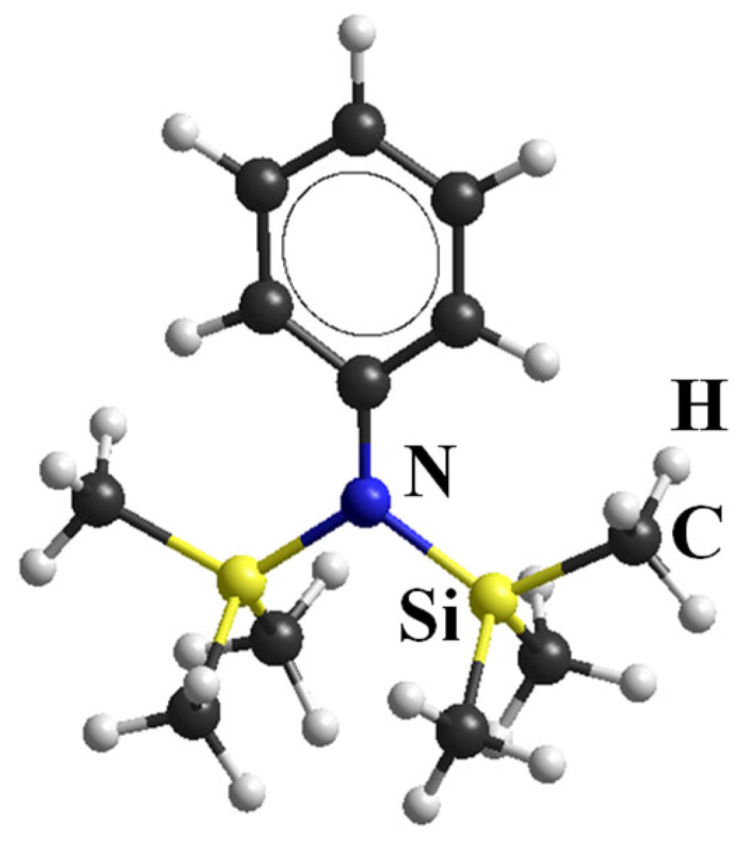
2.1. Materials
2.2. PECVD
2.3. Characterization of Chemical Bonding Structure and Surface Morphology
2.4. Optical Properties
2.5. Porosity
2.6. Dielectric Constant
3. Results and Discussion
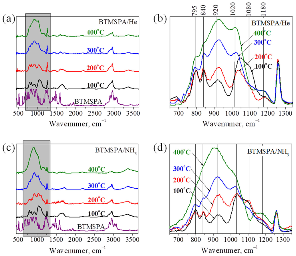
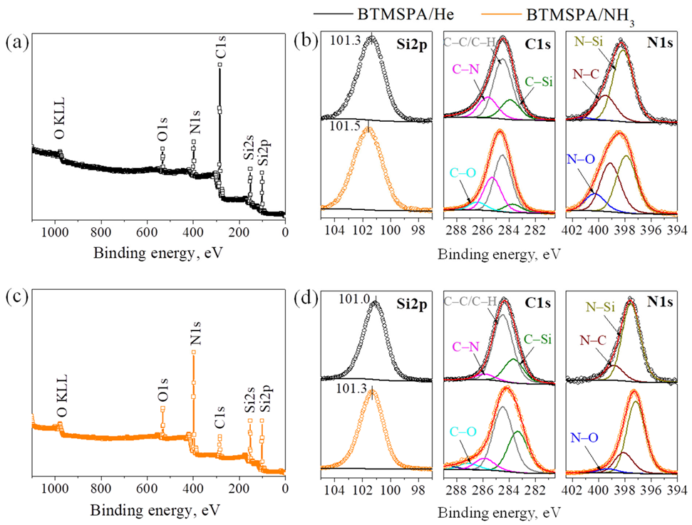
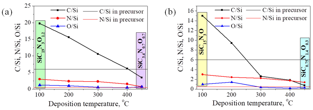
3.1. Chemical Bonding Structure and Elemental Composition
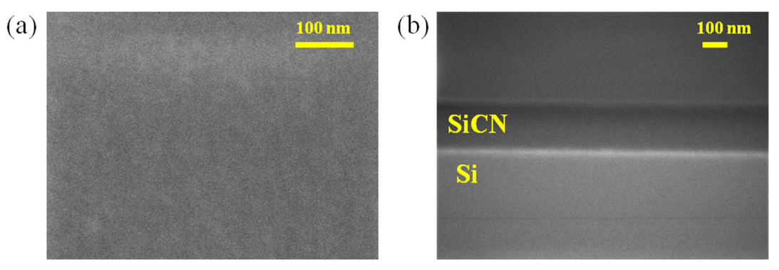
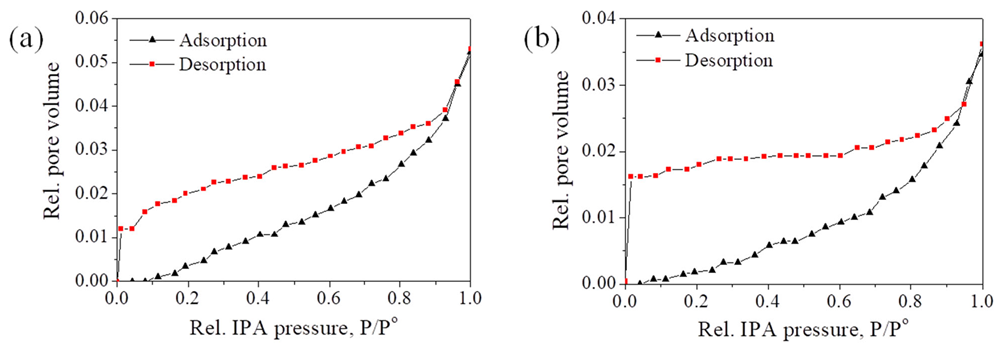
3.2. Microstructure and Porosity
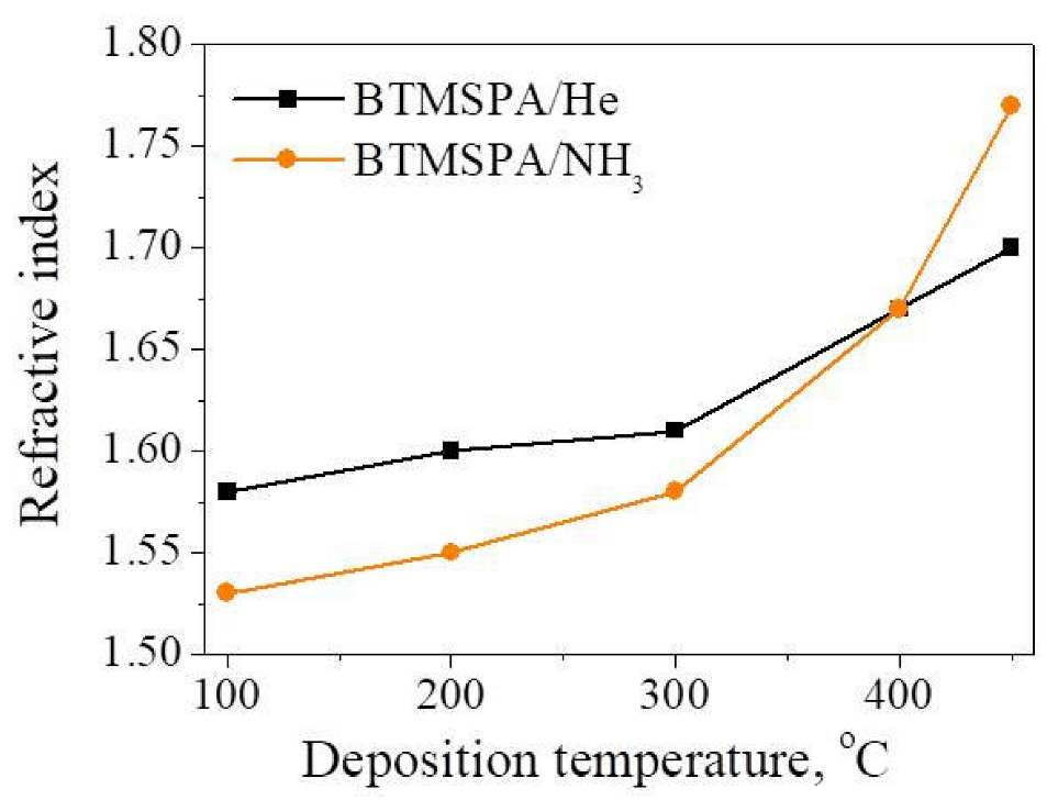
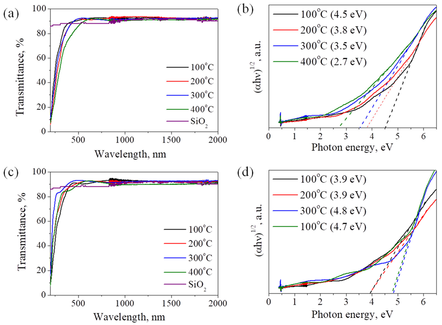
3.3. Optical Properties
3.4. Dielectric Properties
3.5. Comparison with the Literature Data
4. Conclusions
Author Contributions
Funding
Institutional Review Board Statement
Informed Consent Statement
Data Availability Statement
Acknowledgments
Conflicts of Interest
References
- Igumenov, I.K.; Lukashov, V.V. Modern Solutions for Functional Coatings in CVD Processes. Coatings 2022, 12, 1265. [Google Scholar] [CrossRef]
- Sukach, A.V.; Tetyorkin, V.V.; Tkachuk, A.I.; Kozak, A.O.; Porada, O.K.; Ivashchenko, V.I. Charge transport in SiCN/Si heterostructures. Mater. Sci. Semicond. Process. 2022, 143, 106515. [Google Scholar] [CrossRef]
- Cheng, Y.-L.; Lin, Y.-L.; Peng, W.-F.; Lee, C.-Y.; Lin, Y.-J. SiOCH Stacked Dielectric: Effects of Deposition Temperature of SiCN Film. ECS J. Solid State Sci. Technol. 2021, 10, 123002. [Google Scholar] [CrossRef]
- Martin, J.; Filipiak, S.; Stephens, T.; Huang, F.; Aminpur, M.; Mueller, J.; Demircan, E.; Zhao, L.; Werking, J.; Goldberg, C.; et al. Integration of SiCN as a low-k etch stop and Cu passivation in a high performance Cu/low k interconnect. In Proceedings of the IEEE 2002 International Interconnect Technology Conference (Cat. No.02EX519), Burlingame, CA, USA, 5 June 2002; p. 42. [Google Scholar] [CrossRef]
- Wrobel, A.M.; Uznanski, P. Hard silicon carbonitride thin-film coatings by remote hydrogen plasma chemical vapor deposition using aminosilane and silazane precursors. 2: Physical, optical, and mechanical properties of deposited films. Plasma Process Polym. 2021, 18, 2000241. [Google Scholar] [CrossRef]
- Porada, O.K.; Kozak, A.O.; Ivashchenko, V.I.; Dub, S.M.; Tolmacheva, G.M. Hard plasmachemical a-SiCN coatings. J. Superhard Mater. 2016, 38, 263. [Google Scholar] [CrossRef]
- Xu, K.; Jiang, M.; Xue, W.; Liao, N. Ultrasensitive piezoresistive behavior of silicon carbonitride thin films by optimizing nanomorphologies. Mater. Today Nano 2022, 20, 100270. [Google Scholar] [CrossRef]
- Silva, J.A.; Quoizola, S.; Hernandez, E.; Thomas, L.; Massines, F. Silicon carbon nitride films as passivation and antireflective coatings for silicon solar cells. Surf. Coat. Technol. 2014, 242, 157. [Google Scholar] [CrossRef]
- Lavareda, G.; Vygranenko, Y.; Amaral, A.; Nunes de Carvalho, C.; Barradas, N.P.; Alves, E.; Brogueira, P. Dependence of optical properties on composition of silicon carbonitride thin films deposited at low temperature by PECVD. J. Non-Cryst. Solids 2021, 551, 120434. [Google Scholar] [CrossRef]
- Semenova, O.I.; Kosinova, M.L.; Li, Z.Y.; Nemkova, A.A.; Yu, Y.D. Silicon Nitride and Carbonitride Films for Waveguide Structures Based on Strained Silicon. Optoelectron. Instrum. Proc. 2019, 55, 462. [Google Scholar] [CrossRef]
- Fainer, N.I.; Kosinova, M.L.; Rumyantsev, Y.M.; Maximovskii, E.A.; Kuznetsov, F.A. Thin silicon carbonitride films are perspective low-k materials. J. Phys. Chem. Solids 2008, 69, 661. [Google Scholar] [CrossRef]
- Szymanowski, H.; Olesko, K.; Kowalski, J.; Fijalkowski, M.; Gazicki-Lipman, M.; Sobczyk-Guzenda, A. Thin SiNC/SiOC Coatings with a Gradient of Refractive Index Deposited from Organosilicon Precursor. Coatings 2020, 10, 794. [Google Scholar] [CrossRef]
- Wrobel, A.M.; Blaszczyk-Lezak, I. Remote Hydrogen Microwave Plasma CVD of Silicon Carbonitride Films from a Tetramethyldisilazane Source. Part 2: Compositional and Structural Dependencies of Film Properties. Chem. Vap. Depos. 2007, 13, 601. [Google Scholar] [CrossRef]
- Guruvenket, S.; Andrie, S.; Simon, M.; Johnson, K.W.; Sailer, R.A. Atmospheric-Pressure Plasma-Enhanced Chemical Vapor Deposition of a-SiCN:H Films: Role of Precursors on the Film Growth and Properties. Appl. Mater. Interfaces 2012, 4, 5293. [Google Scholar] [CrossRef]
- Izumi, A.; Oda, K. Deposition of SiCN films using organic liquid materials by HWCVD method. Thin Solid Films 2006, 501, 195. [Google Scholar] [CrossRef]
- Fainer, N.I. From organosilicon precursors to multifunctional silicon carbonitride. Rus. J. Gen. Chem. 2012, 82, 43. [Google Scholar] [CrossRef]
- Ermakova, E.; Lis, A.; Kosinova, M.; Rumyantsev, Y.; Maximovskii, E.; Rakhlin, V. Bis(trimethylsilyl)ethylamine: Synthesis, properties and its use as CVD precursor. Phys. Proc. 2013, 46, 209. [Google Scholar] [CrossRef] [Green Version]
- Cheng, Y.-L.; Lin, Y.-L. Comparison of SiCxNy barriers using different deposition precursors capped on porous low-dielectric-constant SiOCH dielectric film. Thin Solid Films 2020, 702, 137983. [Google Scholar] [CrossRef]
- Ma, X.; Xu, C.; Mao, Z.; Ji, P.; Jin, C.; Xu, D.; Ding, Y. Synthesis, characterization, and thermal properties of novel silicon 1,1,3,3-tetramethylguanidinate derivatives and use as single-source chemical vapor deposition precursors. Appl. Organomet. Chem. 2020, 34, e5349. [Google Scholar] [CrossRef]
- Ng, Y.M.; Ong, C.W.; Zhao, X.A.; Choy, C.L. Polymerization of dual ion beam deposited CNx films with increasing N content. Vacuum Sci. Technol. 1999, 17, 584. [Google Scholar] [CrossRef]
- Fainer, N.I.; Plekhanov, A.G.; Golubenko, A.N.; Rumyantsev, Y.M.; Rakhlin, V.I.; Maximovski, E.A.; Shayapov, V.R. PECVD Synthesis of Silicon Carbonitride Layers Using Methyltris(diethylamino)silane as the New Single-Source Precursor. J. Solid State Sci. Technol. 2015, 4, 3153. [Google Scholar] [CrossRef]
- Fainer, N.I.; Golubenko, A.N.; Rumyantsev, Y.M.; Kesler, V.G.; Ayupov, B.M.; Rakhlin, V.I.; Voronkov, M.G. Tris(diethylamino)silane—A new precursor compound for obtaining layers of silicon carbonitride. Glass Phys. Chem. 2012, 38, 15. [Google Scholar] [CrossRef]
- Wrobel, A.M.; Blaszczyk-Lezak, I.; Uznanski, P.; Glebocki, B. Remote Hydrogen Microwave Plasma Chemical Vapor Deposition of Amorphous Silicon Carbonitride (a-SiCN) Coatings Derived From Tris(dimethylamino)Silane. Plasma Process. Polym. 2011, 8, 542. [Google Scholar] [CrossRef]
- Zhou, Y.; Probst, D.; Thissen, A.; Kroke, E.; Riedel, R.; Hauser, R.; Hoche, H.; Broszeit, E.; Kroll, P.; Stafast, H. Hard silicon carbonitride films obtained by RF-plasma-enhanced chemical vapour deposition using the single-source precursor bis(trimethylsilyl)carbodiimide. J. Europ. Ceram. Soc. 2006, 26, 1325. [Google Scholar] [CrossRef]
- Smirnova, T.P.; Badalyan, A.M.; Yakovkina, L.V.; Sysoeva, N.H.; Asanov, I.P.; Kaichev, V.V.; Bukhtiarov, V.I.; Shmakov, A.N. Silicon carbonitride films synthesized from new sources. Chem. Sustain. Dev. 2001, 9, 23–29. [Google Scholar]
- Ermakova, E.; Kosinova, M. Organosilicon compounds as single-source precursors for SiCN films production. J. Organomet. Chem. 2022, 958, 122183. [Google Scholar] [CrossRef]
- Chang, W.Y.; Chang, C.Y.; Leu, J. Optical properties of plasma-enhanced chemical vapor deposited SiCxNy films by using silazane precursors. Thin Solid Films 2017, 636, 671. [Google Scholar] [CrossRef]
- Sobczyk-Guzenda, A.; Oleśko, K.; Gazicki-Lipman, M.; Szymański, W.; Balcerzak, J.; Wendler, B.; Szymanowski, H. Chemical structure and optical properties of a-SiNC coatings synthesized from different disilazane precursors with the RF plasma enhanced CVD technique—A comparative study. Mater. Res. Express 2019, 6, 016410. [Google Scholar] [CrossRef]
- Chen, C.W.; Huang, C.C.; Lin, Y.Y.; Chen, L.C.; Chen, K.H.; Su, W.F. Optical properties and photoconductivity of amorphous silicon carbon nitride thin film and its application for UV detection. Diamond Relat. Mater. 2005, 14, 1010. [Google Scholar] [CrossRef]
- Kafrouni, W.; Rouessac, V.; Julbe, A.; Durand, J. Synthesis of PECVD a-SiCXNY:H membranes as molecular sieves for small gas separation. J. Membr. Sci. 2009, 329, 130. [Google Scholar] [CrossRef]
- Chang, W.Y.; Chen, Y.Z.; Lee, H.T.; Leu, J. Embedded carbon bridges in low-k PECVD silicon carbonitride films using silazane precursors. Jpn. J. Appl. Phys. 2019, 58, SHHB01. [Google Scholar] [CrossRef]
- Fainer, N.; Rumyantsev, Y.; Kosinova, M.; Maximovski, E.; Kesler, V.; Kirienko, V.; Kuznetsov, F. Low-k dielectrics on base of silicon carbon nitride films. Surf. Coat. Technol. 2007, 201, 9269. [Google Scholar] [CrossRef]
- Mera, G.; Riedel, R.; Poli, F.; Müller, K. Carbon-rich SiCN ceramics derived from phenyl-containing poly(silylcarbodiimides). J. Eur. Ceram. Soc. 2009, 29, 2873. [Google Scholar] [CrossRef]
- Rezvanov, A.A.; Vishnevskiy, A.S.; Seregin, D.S.; Schneider, D.; Lomov, A.A.; Vorotilov, K.A.; Baklanov, M.R. Benzene bridged hybrid organosilicate films with improved stiffness and small pore size. Mater. Chem. Phys. 2022, 290, 126571. [Google Scholar] [CrossRef]
- Uchida, Y.; Katoh, T.; Sugahara, S.; Matsumura, M. Chemical Vapor Deposition Based Preparation on Porous Silica Films. Jpn. J. Appl. Phys. 2000, 39, L1155. [Google Scholar] [CrossRef]
- Ermakova, E.; Mogilnikov, K.; Rumyantsev, Y.; Kichay, V.; Maximovskii, E.; Semenova, O.; Kosinova, M. Study of Cu diffusion behavior in carbon rich SiCN:H films deposited from trimethylphenylsilane. Thin Solid Films 2015, 588, 39. [Google Scholar] [CrossRef]
- Rumyantsev, Y.M.; Fainer, N.I.; Ayupov, B.M.; Rakhlin, V.I. Plasma enhanced chemical deposition of nanocrystalline silicon carbonitride films from trimethyl(phenylamino)silane. Glass Phys. Chem. 2011, 37, 316. [Google Scholar] [CrossRef]
- Ermakova, E.N.; Sysoev, S.V.; Nikulina, L.D.; Tsyrendorzhieva, I.P.; Rakhlin, V.I.; Kosinova, M.L. Synthesis and characterization of organosilicon compounds as novel precursors for CVD processes. Thermochim. Acta 2015, 622, 2. [Google Scholar] [CrossRef]
- Baake, O.; Hoffmann, P.S.; Kosinova, M.L.; Klein, A.; Pollakowski, B.; Beckhoff, B.; Fainer, N.I.; Trunova, V.A.; Ensinger, W. Analytical characterization of BCxNy films generated by LPCVD with triethylamine borane. Anal. Bioanal. Chem. 2010, 398, 1077. [Google Scholar] [CrossRef]
- Tauc, J.; Grigorovici, R.; Vancu, A. Optical Properties and Electronic Structure of Amorphous Germanium. Phys. Stat. Sol. B 1966, 15, 627. [Google Scholar] [CrossRef]
- Baklanov, M.R.; Mogilnikov, K.P. Non-destructive characterisation of porous low-k dielectric films. Microelectron. Eng. 2002, 64, 335. [Google Scholar] [CrossRef]
- Peter, S.; Bernütz, S.; Berg, S.; Richter, F. FTIR analysis of a-SiCN:H films deposited by PECVD. Vacuum 2013, 98, 81. [Google Scholar] [CrossRef]
- Chagin, M.N.; Sulyaeva, V.S.; Shayapov, V.R.; Kolodin, A.N.; Khomyakov, M.N.; Yushina, I.V.; Kosinova, M.L. Synthesis, Properties and Aging of ICP-CVD SiCxNy:H Films Formed from Tetramethyldisilazane. Coatings 2022, 12, 80. [Google Scholar] [CrossRef]
- Ivashchenko, V.I.; Porada, O.K.; Kozak, A.O.; Manzhara, V.S.; Sinelnichenko, O.K.; Ivashchenko, L.A.; Shevchenko, R.V. An effect of hydrogenation on the photoemission of amorphous SiCN films. Int. J. Hydrogen Energy 2022, 47, 7263. [Google Scholar] [CrossRef]
- Jiang, H.; Johnson, W.E.; Grant, J.T.; Eyink, K.; Johnson, E.M.; Tomlin, D.W.; Bunning, T.J. Plasma Polymerized Multi-Layered Photonic Films. Chem. Mater. 2003, 15, 340. [Google Scholar] [CrossRef]
- Jobanputra, M.C.; Durstock, M.F.; Clarson, S.J. Investigation of plasma polymerized benzene and furan thin films for application in opto-electronic devices. J. Appl. Polym. Sci. 2003, 87, 523. [Google Scholar] [CrossRef]
- Kilicaslan, A.; Levasseur, O.; Roy-Garofano, V.; Profili, J.; Moisan, M.; Côté, C.; Sarkissian, A.; Stafford, L. Optical emission spectroscopy of microwave-plasmas at atmospheric pressure applied to the growth of organosilicon and organotitanium nanopowders. J. Appl. Phys. 2014, 115, 113301. [Google Scholar] [CrossRef]
- Granier, A.; Vervloet, M.; Aumaille, K.; Vallée, C. Optical emission spectra of TEOS and HMDSO derived plasmas used for thin film deposition. Plasma Sources Sci. Technol. 2003, 12, 89. [Google Scholar] [CrossRef]
- Peter, S.; Speck, F.; Lindner, M.; Seyller, T. Analysis of a-SiCN:H films by X-ray photoelectron spectroscopy. Vacuum 2017, 138, 191. [Google Scholar] [CrossRef]
- Kumar, D.; Swain, B.P. Investigation of structural and mechanical properties of silicon carbonitride thin films. J. Alloys Compd 2019, 789, 295. [Google Scholar] [CrossRef]
- Park, Y.B.; Rhee, S.W. Bulk and interface properties of low-temperature silicon nitride films deposited by remote plasma enhanced chemical vapor deposition. J. Mater. Sci. Mater. Electron 2001, 12, 515. [Google Scholar] [CrossRef]
- Baklanov, M.R.; Mogilnikov, K.P.; Polovinkin, V.G.; Dultsev, F.N. Determination of pore size distribution in thin films by ellipsometric porosimetry. J. Vac. Sci. Technol. B 2000, 18, 1385. [Google Scholar] [CrossRef]
- Hegedüs, N.; Lovics, R.; Serényi, M.; Zolnai, Z.; Petrik, P.; Mihály, J.; Fogarassy, Z.; Balázsi, C.; Balázsi, K. Examination of the Hydrogen Incorporation into Radio Frequency-Sputtered Hydrogenated SiNx Thin Films. Coatings 2021, 11, 54. [Google Scholar] [CrossRef]
- Hegedüs, N.; Balázsi, K.; Balázsi, C. Silicon Nitride and Hydrogenated Silicon Nitride Thin Films: A Review of Fabrication Methods and Applications. Materials 2021, 14, 5658. [Google Scholar] [CrossRef] [PubMed]
- Mahi, C.; Brinza, O.; Issaoui, R.; Achard, J.; Bénédic, F. Synthesis of High Quality Transparent Nanocrystalline Diamond Films on Glass Substrates Using a Distributed Antenna Array Microwave System. Coatings 2022, 12, 1375. [Google Scholar] [CrossRef]
- Adarsh, K.V.; Naik, R.; Sangunni, K.S.; Kokenyesi, S.; Jain, H.; Miller, A.C. Kinetics and chemical analysis of photoinduced interdiffusion in nanolayered Se/As2S3Se/As2S3 films. J. Appl. Phys. 2008, 104, 053501. [Google Scholar] [CrossRef] [Green Version]
- Naik, R.; Ganesan, R.; Adarsh, K.V.; Sangunni, K.S.; Takats, V.; Kokenyesi, S. In situ pump probe optical absorption studies on Sb/As2S3 nanomultilayered film. J. Non-Cryst. Solids 2009, 355, 1943. [Google Scholar] [CrossRef]
- Zanatta, A.R.; Chambouleyron, I. Absorption edge, band tails, and disorder of amorphous semiconductors. Phys. Rev. B 1996, 53, 3833. [Google Scholar] [CrossRef] [Green Version]
- Dong, H.; Chen, K.; Yang, H.; Ma, Z.; Xu, J.; Li, W.; Yu, L.; Huang, X. Innovative all-silicon based a-SiNx:O/c-Si heterostructure solar-blind photodetector with both high responsivity and fast response speed. APL Photonics 2022, 7, 026102. [Google Scholar] [CrossRef]
- Wrobel, A.M.; Uznanski, P. Hard silicon carbonitride thin-film coatings produced by remote hydrogen plasma chemical vapor deposition using aminosilane and silazane precursors. 1: Deposition mechanism, chemical structure, and surface morphology. Plasma Process. Polym. 2021, 18, 2000240. [Google Scholar] [CrossRef]
- Sinha, A.K.; Lugujjo, E. Lorentz-Lorenz correlation for reactively plasma deposited Si-N films. Appl. Phys. Lett. 1978, 32, 245. [Google Scholar] [CrossRef]
- Khatami, Z.; Bleczewski, L.; Neville, J.J.; Mascher, P. X-ray Absorption Spectroscopy of Silicon Carbide Thin Films Improved by Nitrogen for All-Silicon Solar Cells. ECS J. Solid State Sci. Technol. 2020, 9, 083002. [Google Scholar] [CrossRef]
- Nguyen, H.H.; Jayapal, R.; Dang, N.S.; Nguyen, V.D.; Trinh, T.T.; Jang, K.; Yi, J. Investigation of charge storage and retention characteristics of silicon nitride in NVM based on InGaZnO channels for system-on-panel applications. Microelectron. Eng. 2012, 98, 34. [Google Scholar] [CrossRef]
- Bachar, A.; Bousquet, A.; Mehdi, H.; Monier, G.; Robert-Goumet, C.; Thomas, L.; Belmahi, M.; Goullet, A.; Sauvage, T.; Tomasella, E. Composition and optical properties tunability of hydrogenated silicon carbonitride thin films deposited by reactive magnetron sputtering. App. Surf. Sci. 2018, 444, 293. [Google Scholar] [CrossRef]
- Saito, N.; Goto, T.; Tomioka, Y.; Yamaguchi, T. Improvement of photoconductivity of a-SiC:H films by introducing nitrogen during magnetron sputtering process. J. Appl. Phys. 1991, 69, 1518. [Google Scholar] [CrossRef]
- Kozak, A.O.; Ivashchenko, V.I.; Porada, O.K.; Ivashchenko, L.A.; Tomila, T.V.; Manjara, V.S.; Klishevych, G.V. Structural, optoelectronic and mechanical properties of PECVD Si–C–N films: An effect of substrate bias. Mater. Sci. Semicon. Proc. 2018, 88, 65. [Google Scholar] [CrossRef]
- Fainer, N.I.; Rumyantsev, Y.M.; Kosinova, M.L.; Yurjev, G.S.; Maximovskii, E.A.; Kuznetsov, F.A. The investigation of properties of silicon nitride films obtained by RPECVD from hexamethyldisilazane. Appl. Surf. Sci. 1997, 113–114, 614. [Google Scholar] [CrossRef]


| Property | Precursor (add. gas) | ||||
|---|---|---|---|---|---|
| Phenyl-Containing Precursors | Disilazane-Based Precursors | ||||
| BTMSPA | TMPS | TMPAS | HMDSN | BTMSEA | |
| Refractive index | 1.58–1.68 (He) 1.53–1.67 (NH3) | 1.62–1.69 (He) 1.53–1.63 (NH3) | 1.5–1.65 (He) 1.32–1.65 (NH3) | 1.5–1.80 (He) 1.52–1.73 (NH3) | 1.54–1.74 (He) 1.47–1.56 (NH3) |
| Optical bandgap | 2.7–4.5 (He) 3.9–4.7 (NH3) | 2.7–3.7 (He) 2.48–4.03 (NH3) | 2.55–3.5 (He) 3.55 (NH3) | 3.2–4.3 (He) 2.2 (NH3) | 4.15–4.37 (He) 3.9–5.12 (NH3) |
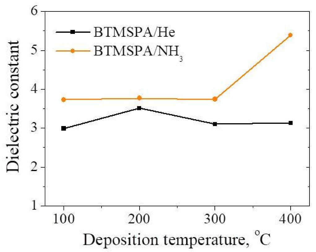
| Permittivity | 2.99–3.51 (He) 3.73–5.39 (NH3) | 2.96–3.73 (He) 3.36–5.29 (NH3) | - | 3–4.2 (He) 4.7–6.2 (NH3) | >5.8 |
| Ref. | This paper | [36] | [5,37] | [11,16,67] | [17] |
Publisher’s Note: MDPI stays neutral with regard to jurisdictional claims in published maps and institutional affiliations. |
© 2022 by the authors. Licensee MDPI, Basel, Switzerland. This article is an open access article distributed under the terms and conditions of the Creative Commons Attribution (CC BY) license (https://creativecommons.org/licenses/by/4.0/).
Share and Cite
Ermakova, E.; Mogilnikov, K.; Asanov, I.; Fedorenko, A.; Yushina, I.; Kichay, V.; Maksimovskiy, E.; Kosinova, M. Chemical Structure, Optical and Dielectric Properties of PECVD SiCN Films Obtained from Novel Precursor. Coatings 2022, 12, 1767. https://doi.org/10.3390/coatings12111767
Ermakova E, Mogilnikov K, Asanov I, Fedorenko A, Yushina I, Kichay V, Maksimovskiy E, Kosinova M. Chemical Structure, Optical and Dielectric Properties of PECVD SiCN Films Obtained from Novel Precursor. Coatings. 2022; 12(11):1767. https://doi.org/10.3390/coatings12111767
Chicago/Turabian StyleErmakova, Evgeniya, Konstantin Mogilnikov, Igor Asanov, Anastasiya Fedorenko, Irina Yushina, Vadim Kichay, Eugene Maksimovskiy, and Marina Kosinova. 2022. "Chemical Structure, Optical and Dielectric Properties of PECVD SiCN Films Obtained from Novel Precursor" Coatings 12, no. 11: 1767. https://doi.org/10.3390/coatings12111767