
Magnetron Sputtering of Transition Metal Nitride Thin Films for Environmental Remediation


1
Physics Department, ABBES Laghrour—Khenchela University, P.O. Box 1252, Khenchela 40004, Algeria
2
Laboratory of Active Components and Materials, Larbi Ben M’Hidi University, Oum El Bouaghi 04000, Algeria
3
LASMIS, Université de Technologie de Troyes, Pôle Technologique Sud Champagne, 26 Rue Lavoisier, 52800 Nogent, France
4
Faculty of Engineering and Environment, Northumbria University, London E1 7HT, UK
5
Institute for Nanotechnology and Water Sustainability, College of Science, Engineering and Technology, University of South Africa, Florida, Johannesburg 1709, South Africa
6
Ecole Polytechnique Fédérale de Lausanne, EPFL-SB-ISIC-GPAO, Station 6, 1015 Lausanne, Switzerland
7
Global Institute for Water, Environment and Health, 1201 Geneva, Switzerland
*
Authors to whom correspondence should be addressed.
Coatings 2022, 12(11), 1746; https://doi.org/10.3390/coatings12111746
Submission received: 19 September 2022
/
Revised: 24 October 2022
/
Accepted: 9 November 2022
/
Published: 14 November 2022
(This article belongs to the Special Issue Bio-Based Packaging Films: Development, Characterization, and Application)
Abstract
:The current economic and ecological situation encourages the use of steel to push the technological limits and offer more cost-effective products. The enhancement of steel properties like wear, corrosion, and oxidation resistance is achieved by the addition of small amounts of chemical elements such as Cr, Ni, Si, N, etc. The steel surface can be protected by different treatments such as heating and coating, among others. For many decades, coatings have been an effective solution to protect materials using thin hard films. Several technologies for thin film deposition have been developed. However, some of them are restricted to certain fields because of their complex operating conditions. In addition, some deposition techniques cannot be applied to a large substrate surface type. The magnetron sputtering deposition process is a good option to overcome these challenges and can be used with different substrates of varying sizes with specific growth modes and for a wide range of applications. In this review article, we present the sputtering mechanism and film growth modes and focus on the mechanical and tribological behavior of nitride thin films deposited by the magnetron sputtering technique as a function of process conditions, particularly bias voltage and nitrogen percentage. The biomedical properties of transition metal nitride coatings are also presented.
1. Introduction
The degradation of a material is one of the most important problems in the industrial domain. Several forms of damage to the material surface produced in an aggressive environment have exposed interesting catalytic properties of hard thin films [1]. Furthermore, to enhance surface properties, extend the service life, and improve the appearance of materials, thin films are frequently used, whether in electronics fields, optics, or in mechanics, the development of different deposition techniques and the control of operating parameters have made it possible to obtain coatings with good wear resistance, very high hardness, and good thermal and chemical stability. The hard materials are generally applied for protecting the cutting tool and giving an economic advantage in the industry. However, they are inadequate to support several mechanical applications (turning, milling, stamping, etc.). Surface treatments remain the adequate solution to improve the performance of a metal surface. These treatments consist of structural transformations, thermo-chemical diffusion treatments, and conversion, which improve the performance of new materials obtained. Thin films are subject to new searches due to the great interest concerning lifetime prolongation in the industrial fields; coated tools offer a two- to fourfold greater lifespan than uncoated tools. In this review, we present a general overview on thin films and their applications, and then we cover the hard coatings and their categories, general information about transition metal nitrides, as well as literature reviews of binary and complex nitride systems [1,2,3,4].
Modern technologies are based on the exploitation of typical thin film properties, such as adhesion, thermal stability, low porosity, and desirable stoichiometry, among others, which are strongly investigated and have become one of the most important industrial interests. For example, transition metal-based thin films (Cr, Ti, Mo, Zr, Ta, etc.) deposited on steel substrates by various conventional techniques exhibit excellent behavior under severe conditions [1,2]. The knowledge of film growth procedure enables the deposition of thin films with desired structure that satisfy a required function. Therefore, it is important to optimize the deposition method to produce good thin films and make remarkable progress in the deposition technologies. Hard film deposition can be carried out largely using two methods: chemical vapor deposition (CVD) and physical vapor deposition (PVD), which have been used in many applications [3,4].
There are many physical vapor deposition (PVD) methods for film fabrication with thicknesses of up to a few micrometers. These PVD techniques include diode sputtering, ion-beam sputtering, and magnetron sputtering [5,6]. Generally, during sputtering, the bombardment of the solid target with high-energy ions in low-pressure plasma results in the deposition and coating of the desired film on a substrate. The sputtered coating particles move from the target, either as atoms, charged ions, or molecules, and condense on the substrate surface. Essentially, the atoms/molecules follow straight trajectories with the possibility to collide with residual gas atoms inside the deposition chamber. Among the PVD techniques, magnetron sputtering has rapidly developed in recent decades. It has become the most widely exploited deposition method in the coatings industry for the deposition of metals, alloys, metal oxides, carbides, nitrides, and cements on a wide range of substrates, i.e., metals, alloys, ceramics, glass, and polymers [7,8,9].
Currently, magnetron sputtering has important advantages in industrial and research fields. In literature, we can find many examples of thin films used for industrial applications such as decorative films, hard films, low-friction films, and corrosion-resistant films [10,11,12,13,14,15,16,17,18,19]. Recent studies have focused on the investigation of the physical mechanisms, such as the interaction between charged particles and the surface of the target, adhesion and chemical reactions between the substrate and the coating, as well as the influence of the deposition parameters, such as temperature, pressure, vacuum, substrate polarization, target power, and deposition time. Generally, most thin films are produced with a high degree of crystallinity. In our recent studies, we investigated the influence of deposition parameters on the structure and tribomechanical behavior of thin films VN, TiN, ZrN, and CrN. To enhance the binary component proprieties, ternary transition metal nitrides were also designed. It was shown that ternary systems offered great enhancements in mechanical and tribological properties, such as low friction and high wear resistance, which are the main characteristics of hard coatings continually employed for the protection of tool surfaces [14,15,16,17,18,19].
Even though there are few available studies, the microstructure and mechanical properties of nitride hard thin films as a function of adding elements have been presented without taking into consideration the correlation between the different deposition parameters. Furthermore, there is no previous review on the effect of transition metals on the mechanical, wear, and antibacterial activity of nitride-based thin films.
In this review article, we specifically describe magnetron sputtering as a typical PVD technique used in the fabrication and processing of thin film technologies. We present a detailed description of the deposition process where the ions are derived from plasma under low-pressure gas between two electrodes, leading to the sputtering of target atoms/molecules on a substrate. The influence of deposition parameters on the film properties and performance are presented, particularly the effect of bias-voltage and nitrogen percentage on the mechanical and tribological behavior of nitride films, as typical examples. The anti-microbial and bactericidal behavior of transition metal nitrides and oxide coatings are detailed, along with an analysis of the influential factors and mechanism of action. The application of the coatings in the degradation of emerging pollutants is also briefly discussed to underpin the importance of magnetron sputtering in environmental pollution remediation.
2. Sputtering Technology
The PVD technique permits the development of coatings at low temperatures (<600 °C) and pressure (<1 Pa). It is among the most economical and ecologically friendly techniques, releasing less harmful pollution to the environment when compared to CVD. Figure 1 presents some examples of thin films deposited by different techniques under different deposition conditions i.e., temperature and pressure. Using the PVD technique, it is possible to control the various deposition parameters, allowing the reproducibility of the experiments with a high deposition rate, which contributes to the cost reduction of this process and increases its productivity [6,7].
The sputtering phenomenon was first observed in the 1850s and then developed around the 1940s when diode sputtering was first used as a commercial coating process [8]. Sputtering is one of the ultra-high vacuums (UHV) PVD processes used for depositing coatings on substrates. The atoms of a solid target are ejected due to the momentum transfer from an atomic-sized energetic bombarding particle impinging on the target surface [8]. The potential difference in the deposition chamber leads to ionization, acceleration, and orientation of argon ions (plasma) to the target. These plasma ions can dislodge the target atoms or molecules, either through direct collision or initiation of a ‘collision cascade’ resulting in the emission of atoms which then condense on a substrate (anode) as a thin film, as illustrated in Figure 2 [8,14]. The sputtering yield depends on the composition of the target material, binding energy of deposited elements, the incident ions, and the deposition parameters, such as pressure, gases, and applied power.
3. Magnetron Sputtering Mechanism
Sputtering has been known for many applications; however, this process is limited by low deposition rate, low ionization efficiency in the plasma, and high substrate heating effects. Alloys and refractory metals cause problems because of differences in their sputtering rates and high melting points. In addition, compounds can dissociate into their chemical constituents at low working pressures [8,21]. These problems have been overcome by the development of magnetron sputtering techniques, as illustrated in Figure 3 [21]. This method depends on the application of a specially shaped magnetic field to the cathode (target) to create electron traps, so that drift currents close on themselves. The applied magnetic field increases the path length of primary and secondary electrons and pushes them to concentrate in a localized region close to the cathode, at lower voltages than diode systems (500–600 V). These electrons play an important role in maintaining the plasma and increasing the probability of collision between ionized atoms and electrons. The high ionization efficiency leads to an increase in ion current density applied to the cathode, which is proportional to the target erosion rate [8].
There are three principal types of magnetron design, including direct current (DC), radio frequency (RF), and reactive magnetron sputtering processes:
3.1. Direct Current (DC) Magnetron Sputtering Mechanism
Direct current magnetron sputtering (DCMS) is one of the simplest and oldest sputtering processes. Initially, the sputtering mainly concentrated on metallic films deposited on metallic substrates. Thus, until the 1960s, this sputtering process was one of the most common techniques available in the market [8]. In this process, the cathode (target) is connected directly to the negative potential of the power supply, and the anode (substrate) is mounted in a low-pressure vacuum chamber. During the sputtering, a negative bias voltage (−V) typically in the range of −2 to −5 kV is applied to the target, where the electrons enter the system. Simultaneously, a positive charge is also applied to the substrate (anode), as shown in the Figure 4a. This initiates the ionization of the inert gas molecules, and these ions and electrons further collide with gas molecules near the cathode to produce secondary electrons which maintain the discharge in the plasma in the range of 10–350 kHz.
In the DC mode, the target is a conductor and can be operated at a maximum power level of about 0.7 W/mm2. For 100 mm circular magnetrons, power supplies must be capable of delivering up to 5 kW into the plasma and generally, the power required is dependent on the size of the target, such that the large magnetrons may consume up to 50 kW [8]. This can increase the deposition rate on static substrates up to several micrometers per minute, making it very suitable for high-production rate processes. Consequently, DCMS is used in different industrial sectors including microelectronic circuits, electrical resistance films (Ni-Cr for strain gauges), magnetic films (Fe, Co-Pt, Co-Cr, Co-Ni), tapes and magnetic film heads, opto-storage devices, corrosion-resistant films (Cr-Ni), glass fibers and gas sensors [8]. However, the main disadvantages of the DCMS include the very low deposition rate (~10–20 nm/min) at commercial scale manufacturing and selectivity, since only conductive materials can be sputtered. Furthermore, the pressure threshold required to achieve plasma can significantly degrade the film quality compared with the RF magnetron sputtering process [22,23].
3.2. Radio Frequency (RF) Magnetron Sputtering Mechanism
In DCMS, a conductive target is required to ensure the flow of current, which means that it cannot be used for sputtering non-conductive target materials. Hence, the need for radio frequency sputtering [8] becomes essential to coat non-conductive thin films. Basically, in radio frequency magnetron sputtering (RFMS), an RF potential is applied to the target using an alternating current at high frequency, typically 13.56 MHz, and the generated electrons move for a long distance during each half cycle, as illustrated in Figure 4b. This increases the probability of further ionization of the inert/process gas atoms and the generation of stable high-density plasma that improves the efficiency of the sputtering process. In addition, the increased ionization efficiency achieved in the RF magnetron process aids in maintaining the discharge at lower operating pressure (1–15 mTorr) and operating voltage (−500 to −1000 V) than those required in the conventional sputtering mode [24,25]. RFMS can be used for the deposition of different types of films such as polymers, ceramics, or insulating compounds, as well as ionic, covalent, and metallic materials. However, RF sputtering requires an impedance-matching network to ensure that the maximum power is absorbed into the plasma. Although RF sputtering equipment (power suppliers in particular) is more expensive than the DC magnetron, the RF magnetron sputtering offers many advantages. These include the use of non-conductive targets, charge-up effects, and reduced arcing due to the use of an alternating electric field. The passivation and insulating properties and electrical resistances of the RF-sputtered films make them an ideal candidate for applications in microelectronic and strain gauges. For example, SiO2 films can separate the resistance element from the basic support; also, the Ni-Cr films can be sputtered to form highly adherent strain-gauge elements [8]. In the RFMS system, the ionized Ar atoms bombard the targets, and their molecules/atoms are released to form thin layers at substrates.
3.3. Reactive Magnetron Sputtering Mechanism
Some dielectric materials can be sputtered by RF or DC magnetron sputtering in a reactive gas atmosphere. Reactive magnetron sputtering process (RMS) is used to form films by co-deposition and reaction of the constituents, or by the reaction of deposited species with the ambient gaseous or vapor environment [2]. Typically, argon gas is injected into the deposition chamber as a carrier gas, mixed with small quantities of a second reactive gas. The reactive gas (typically nitrogen or oxygen) used during the sputtering process reacts with the target surface as well as the sputtered metal atoms and thus forms a thin film on the substrate surface, as depicted in Figure 4c. These reactions affect the whole procedure [26]. A film will only be formed if the product of the reacting species is nonvolatile. Also, co-deposition of reactive species does not necessarily guarantee the activation of a chemical reaction and subsequent film deposition on the substrate [2]. Reactive sputter deposition may also occur if the sputtered particles react with adsorbed species already present on the substrate surface (e.g., contaminants). Generally, for depositing at low temperatures, some of the reacting species should be condensable with the other gaseous ones [2].
Figure 4.
Schematic view of (a) direct current (b) radio frequency, and (c) reactive magnetron sputtering systems Reprinted from Refs. [24,27].

Reactive sputtering can be used for depositing films by a chemical reaction between the target material and the gas introduced into the vacuum chamber where the compositions of these films can be controlled by adjusting the relative pressure of the mixture between Ar ions and reactive gases. The reactive magnetron sputtering can be used not only for sputtering of nitrides, oxides, carbides, and other compounds, but also to produce nanocomposite films with small grain size (1–20 nm) [21], which exhibit unique properties and enhance their performance and applications. Hard materials such as titanium nitride (TiN) are used for wear-resistant tools and decorative coatings of watches. The transparent conductor thin films of indium-selenium (In-Sn) oxide are also produced by reactive sputtering. These films are used for electromagnetic interference, liquid crystal displays (LCD), heated screens for vehicles and aircraft, and solar collector panels [2]. Notably, an increase in the flow rate of the reactive gas usually results in the formation of the sputtered compound on the surface of the target (target poisoning). This causes a decline in the sputtering rate and a further poisoning of the target surface [8]. For example, the sputtering of an oxide-covered target is generally not desirable because the sputtering rate of the oxide is much lower than that of the metal, and the development of an insulating surface on the cathode causes arcs, especially when applying DC. In addition to the possible optimization of the ratio of reactive gas and sputtering gas, the solution would be adopting a medium-frequency power or choosing an RF power. Target poisoning is more significant for some oxides, such as aluminum and titanium oxides, because the deposition rate of the oxides is unacceptably low. However, oxides of materials such as indium, zinc, and tin can are sputtered from a metal-oxide target using DC mode, without arcing, and largely have been used for the coating of architectural glass. To decrease the influence of arcing effect, alternating voltages can be applied to prevent the building up of charges in the dielectric layer at the target surface [27].
4. Nucleation and Growth Modes of Sputtered Thin Films
To optimize different properties of thin films, it is necessary to understand their growth mechanisms. The formation of the continuous film involves nucleation and growth on the surface of substrate. The different growth stages are influenced by the mobility of the condensed species, their incidence energy, and substrate temperature and ion bombardment [27,28]. All the processes of thin film growth from a vapor phase are summarized in three principal steps: initially, production of the appropriate species to be deposited on the substrates (ionic, atomic, or molecular compounds) by the Ar+ etching of the target surface. Then, transport of these species from the source (target) to the substrate surface with or without collisions between atoms and molecules. Finally, the condensation of these species by chemical or electrochemical reactions and forming film on the substrate surface. This process involves the condensation of vapor species on the substrate and the formation of the first layers by the nucleation and growth processes. These are strongly influenced by the ionic bombardment of the growing film species leading to changes in microstructure, composition, impurities, and residual stresses [10]. The essential phases of thin film formation from nucleation to growth modes are described below in detail.
Nucleation: Sputtered adatoms arriving on the substrate lose their kinetic energy (physically diffused from the target surface). Thermodynamically, these species are not in equilibrium with the substrate and move over the entire surface. In this state, these species interact with each other and form clusters, and these clusters are unstable and tend to be adsorbed. Under certain deposition conditions, they collide with other adsorbed species and start growing. After reaching a critical size, these clusters become thermodynamically stable, and the nucleation barrier is over. The clusters grow by size and number to reach a maximum density of nucleation, and this is called the nucleation stage. The cluster size depends on many parameters, such as sputtering rate, activation energy, thermal diffusion, and the substrate type. The film in the form of an island can grow parallel or vertical by diffusion of the sputtered species to the substrate surface. In a PVD process, vertical growth at this stage is more important than the in-plane (lateral) one. In the lateral growth, the film became denser and more compact; however, in the vertical growth the structure has a columnar structure and contains more defects and voids. While these defects decrease the cohesion between the sputtered atoms, they have been seen to facilitate the charge transfer and reduce the inward charge recombination when we deal with photo-responsive thin films [13].
Coalescence: The islands grow larger and eventually meet to form a continuous layer. As soon as two islands are close enough to interact, they begin restructuring to minimize their total surface and interface energy. The islands move from a discontinuous type to form grain boundaries, leaving channels and holes in the thin film deposited on the substrate [29]. Atoms diffuse into the neck between the grains to minimize their chemical potential by moving from regions with a positive curvature to the neck, which has a negative curvature. The film growth models are described below in detail.
4.1. Thin Film Growth at a Granular Scale
There are three different initial growth modes of grain boundaries: Volmer-Weber mode, Frank-van der Merwe mode, and Stranski-Krastanov growth mode, as illustrated in Figure 5 and described below in detail.
- Volmer-Weber mode (3D-island growth): Small clusters of atoms directly nucleate on the substrate and then grow in three dimensions in the form of islands. This happens when the deposited atoms are more strongly bonded to each other than to the substrate (Figure 5a). For example, the Ni films deposited an ultra-high vacuum e-beam evaporation system can grow with the Volmer-Weber mode with more residual stress [27].
- Frank-van der Merwe mode (2D-layer growth): In this mode, the growth takes place in two dimensions, filling up one atomic layer before forming the next one, and the atoms are more strongly bonded to the substrate than to each other (Figure 5b) [30,31,32,33].The transition from 3D island growth mode at low temperatures to 2D growth at higher temperatures was observed for indium tin oxide film deposited by PLD on glass [33].
4.2. Thin Film Growth at Microstructure Scale
Many factors affect the growth, structure, and properties of the deposited film, such as substrate temperature, reactive gas, pressure, and contamination of the substrate surface. Among these, the temperature and pressure are two very important parameters affecting film properties. Modern deposition techniques such as sputtering can yield a wide variety of coatings depending on the mobility of the deposited atoms on the substrate surface, which can be enhanced by increasing the temperature during the deposition process. High mobility of the atoms gives more chance of growing highly crystalline thin films, while low mobility of atoms leads to the formation of amorphous films [32]. To explain the influence of the deposition parameters on the coating structure, several researchers [31,32,33] have determined many structural zone models (SZM) representing the growth mode of thin films according to the temperature and working pressure.
Movchan and Demchishin presented a three-zone model for very thick films made by evaporation at varying temperature [34]. This model was further modified and improved by Thornton, who expanded it to include the effects of working pressure (P) and the temperature ratio of substrate to film (Ts/Tf). Furthermore, a transition zone (T) was also considered between zones 1 and 2, described in the following paragraphs. With this extension, the model is now well-known as the Movchan-Demchishin-Thornton (MDT) model [32].
Referring to Figure 6, there are four major structural growth zones referred to as Zone 1, 2, 3, and transition zone attributed to amorphous, crystalline, and granular structures. Growth in Zone 1 is obtained at a low (Ts/Tf < 0.3) ratio and dominated by a low mobility of adatoms. It consists of tapered columns separated by voids and is usually referred to as cauliflower morphology with dome tops. The resulting films are amorphous or nano-crystalline with self-shadowing effects [33].
Zone 2 (0.3 < Ts/Tf < 0.5) is characterized by uniform crystalline columns growing continuously from the surface of the substrate, and the grain size increases and may extend through the film thickness. The surface ends of the grains lead to a faceted surface [32,33].
Zone T (0.2 < Ts/Tf < 0.4): transition morphology occurs at low temperature and gas pressure, similar to zone 2. It is characterized by dense fibrous grains with very low surface roughness. These films can be amorphous or nanocrystalline, and the grain boundary diffusions are strongly limited, leading to competitive grain growth and V-shaped grains with a heterogeneous grain structure. At higher temperatures, bulk diffusion and recrystallization lead to dense films with large grains.
Zone 3 (0.5 < Ts/Tf < 0.75): the structure is characterized by equiaxed (globular) three-dimensional grains, which is a direct indication that the crystal growth has been blocked periodically. This kind of structure is generally attributed to the high-substrate temperature range. For Ts/Tf ≥ 0.75, crystallization and grain growth become important [32,33].
Recently, Anders reported an expansion of Thornton’s model [34], as depicted in Figure 6. The updated model replaced the Ts/Tf ratio with the generalized temperature T*, which includes the homologous temperature and the temperature shift caused by the potential energy of particles arriving on the surface. The linear pressure was also replaced by a logarithmic axis representing the normalized energy flux E*, describing displacement and heating effects caused by the kinetic energy of bombarding particles. Finally, a z-axis is placed for the net film thickness t*, which can be negative in the case of ionic etching [33].
5. Mechanical and Tribological Behavior of Sputtered Thin Films
The process parameters significantly influence mechanical properties and tribological performance of sputtered thin films. Substrate bias voltage, working pressure, electrostatic potentials, magnetic fields, thermal environment, and process and working gas and their kinetics significantly drive plasma dynamics, which influence the coating growth in certain zones, as described in Section 4.2. The bias voltage and process gas have notable impacts on mechanical and tribological behavior of sputtered coatings when compared to other parameters; this is discussed below in detail by representing a case study of nitride-based thin films.
5.1. Sputter Deposition of Binary Transition Nitride Thin Films
5.1.1. Effect of Bias Voltage on Sputter Deposition of Binary Transition Nitride Thin Films
Surface enhancement by means of thin film deposition is an important industrial and research field adopted to protect engineering materials against wear, fatigue, corrosion, and any other damage phenomena [35,36,37,38,39,40]. The magnetron sputtering methods provide great flexibility for designing films with specific chemical composition and microstructure, leading to coatings with excellent properties. Among these films, transition metal coatings deposited (Table 1) on different substrates have shown exceptional improvement in the surface properties, such as low friction coefficient, high hardness, and good wear and corrosion resistances [14].
Thin films of binary nitrides (e.g., Cr-N, Zr-N, and V-N) were deposited using a RF reactive magnetron sputtering method with varying bias voltage to study its effect on the mechanical and tribological behavior of the coatings. Figure 7 shows the main results obtained for these films, and it can be observed that the compressive residual stresses, determined by Stoney’s equation, generally remained lower than 4 GPa for all types of coatings under investigation. The residual stress decreased with increasing bias-voltage, although for some films (e.g., V-N film) the variation was negligible (Figure 7a). Application of substrate bias increases the movement of atoms and charged ions, and they arrive at substrate with more energy and form a dense structure. There is an optimum amount of bias voltage before which the residual stresses increase in the coatings and after whichthe residual stress starts reducing due to a relaxing phenomenon. The hardness of the thin films (Cr-N, Zr-N, and V-N) deposited on XC100 steel substrates is presented in Figure 7b. It is notable that film hardness takes the same trend of residual stress curves. The hardness of nitride films is two to three times higher than that of XC100 steel substrate (6 GPa). Generally, Cr-N and Zr-N nitrides are harder than V-N film. Moreover, it has been shown that hardness decreased with increasing bias voltage. This could be attributed to the increase in ion bombardment energy on the substrate surface increasing the adatoms mobility and producing thick films with higher atomic disorder. Figure 7c presents the variation of friction coefficient (FC, μ) of films as a function of bias voltage, which is calculated from: . The tribological behavior of these films was evaluated using a pin-on-disk configuration with a 100C6 ball. Clearly, increasing the bias voltage led to an increase in the friction coefficients of the films. The friction coefficient of Cr-N and Zr-N is in the range of 0.6–0.42, respectively. The abrupt increase of friction coefficient value (0.83) of V-N thin film is probably due to the formation of vanadium oxides in tribo-induced process nitride and likely increased surface roughness, which strongly influences the wear performance of the surface [14]. The results suggest that Zr-N has presented better hardness and friction coefficient over Cr-N and V-N coatings.
5.1.2. Effect of Nitrogen Percentage on Sputter Deposition of Binary Transition Nitride Thin Films
The X-N transition metal nitride films usually consist of two types of nitrides, i.e., hexagonal X2N (from 30.3 to 33.3 at % of N) and cubic XN (from 49.5 to 50.0 at % of N) [36]. It has been shown that depending on the nitrogen flow rate, X, X2N, and XN phases can be identified. Compared with the fourth (Ti-N, Zr-N, Hf-N) and fifth (V-N, Nb-N, Ta-N) groups of transition metal nitride, the sixth group (Cr-N, Mo-N, W-N) of transition metals are more difficult to react with nitrogen [36,37]. Bertrand et al. [38] found that the mechanical properties highly depend on the N content and the crystalline structure of the transition metal nitride films. CrNx, VNx, and ZrNx thin films were deposited using the reactive magnetron sputtering method at 0, 5, 10, 15, 20, and 25 % of N2 in the (N2+Ar) gas mixture atmosphere. The influence of nitrogen percentage in the deposition atmosphere (Ar+N2) on the phase structures, residual stress, hardness, and friction coefficient of sputtered CrNx, VNx, and ZrNx films was investigated. The XRD analysis reveals the phases of CrNx, VNx, and ZrNx films changed respectively from Cr+Cr2N, V+V2N, and Zr+Zr2N at 5%N2 to Cr2N, V2N, and Zr2N at 10 %N2, and then from phase mixture of Cr2N + CrN, V2N +VN, and Zr2N + ZrN at 15% N2 to nearly CrN, VN, and ZrN phases at 20%N2 [12,14,36,39].
The changes in metallurgical phases have a clear impact on their mechanical properties and tribological performance. Figure 8a shows the residual stresses engendered in CrNx, VNx, and ZrNx coatings during sputtering processes under different percentages of nitrogen. At 0 % N2, the coatings exhibit tensile residual stress in a magnitude of 0.75 GPa (Cr), 0.41 GPa (V), and 0.62 GPa (Zr). The tensile stresses are attributed to the loose structure of the pure chromium, vanadium, and zirconium coatings [39]. The tensile stresses transformed into compressive residual stress for the nitrogen percentage in argon range between 5 and 20% N2. A gradual increase in compressive residual stress was observed up to −2GPa (CrNx), −0.91 GPa (VNx), and −2.4 GPa (ZrNx) as the structure became denser [12,40]. Then, the residual stress of the coatings slightly decreased to −1.5 GPa (CrNx), −0.9GPa (VNx), and −2GPa (ZrNx) with increasing nitrogen from 20 to 25%. This is associated with a significant reduction in the concentration of deposited pure Cr, V, and Zr elements in the coatings. The hardness values of the Cr, V, and Zr coatings, grown without injecting N2, are in the range of 6.8–10 GPa(Figure 8 b) [29]. The coatings deposited at 5% N2 having Cr + Cr2N phases (V + V2N; Zr +Zr2N) exhibited a slightly higher hardness (Figure 8b). The variation in hardness with an increase in nitrogen could be attributed to structural growth. According to the Hall–Petch relationship [12,36], the low hardness was related to the large grain size. Also, the existence of metallic Cr, V, and Zr elements in excess that possess low hardness may be another reasonable explanation for the low hardness [36]. It seems that maximal hardness values were achieved when hard phases of CrN, VN, and ZrN films were generated at 20 %N2, which can be attributed to the high residual stresses, grain refinement, and compactness of films [37].
The tribological properties of transition metal nitride films were determined using a ball-on-disc tribometer with 100Cr counterpart. Figure 8c presents the friction coefficient of the CrNx, VNx, and ZrNx films as a function of the nitrogen percentage. Generally, the friction coefficient ranged between 0.70 and 0.83 for pure Cr, V, and Zr coatings. At first, the friction coefficient decreased and then increased with a further increase in the nitrogen content. Pure Zr, Cr, and V metals have comparable trends of friction coefficient when deposited in absence of nitrogen, and the friction coefficients were in the range of 0.70 to 0.85. The high friction coefficient is attributed to low residual stress and the joint phases of Cr+Cr2N (V+V2N; Zr+Zr2N) that could be responsible for the high friction coefficient. Meanwhile, the hardness of the coating-substrate system and plastic deformation of soft substrate caused cracks in the coatings, leading to a high friction coefficient; in this case, the wear of the film surface dominated the tribological behavior. However, addition of nitrogen has generally reduced the friction coefficient. The film deposited at 20 % N2 exhibited the lowest friction coefficient of 0.53 (CrN), 0.7 (VN), and 0.45 (ZrN). This may be due to the high hardness and adhesion between the film and the steel substrate having high resistance to plastic deformation. Bertrand et al. [41] obtained similar results. However, at 10% N2, the nitride films consisting of Cr2N, V2N, and Zr2Nphases showed higher friction coefficients than those obtained for the films having CrN, VN, and ZrN structure (films deposited at 20% N2).
5.1.3. Effect of Coating Architecture
Despite their reduced hardness compared to monolayers, multilayer coatings are designed principally to achieve the right combination of stiffness, hardness, and toughness. With well-selected interlaying characteristics, through-thickness cracks, deflection at interfaces between layers could be inhibited, leading to enhanced toughness. Furthermore, multilayer films have presented exceptional awareness to further improve the properties of the related binary compounds. Many researchers have studied the influence of depositing multilayers of a coating via magnetron sputtering on the hardness, adhesion, and wear resistance. Cr-based alloy multilayer films are typical examples of these kinds of coatings. Vyas et al. have shown that coating Si and steel substrates with nanometer-scale layers of Cr/CrN (2–3 nm) led to a significant increase in their hardness (>50 GPa) [42]. Generally, Cr/CrN multilayer coatings have been extensively studied due to their high hardness and excellent wear and corrosion resistances. Wiecinski et al. showed that for magnetron-sputtered CrN/Cr multilayer coating with different Cr-CrN bilayers, the increase in Cr/CrN bilayers from 16 to 32 resulted in an increase in hardness from 15 GPa to 16 GPa and a decrease of friction coefficient from 0.65 to 0.17 (Figure 9a) [43]. By studying the influence of film thickness of Cr and CrN bilayers (at 1000, 270, and 110 nm) on the Cr/CrN multilayer coatings, Song et al. showed that the CrN monolayer was harder than the Cr/CrN multilayer coating, and the hardness decreased with the shortening of the bilayer alternation. This is attributed to the nitride effect, which prevented the movement of dislocations through the formation of the hard CrN phase [44]. It has been reported that Cr/Cr2N/CrN multilayer coatings have better performance than CrN single-layer coatings in abrasion and sliding wear tests, and the hardness (20 GPa) was much higher than that of Cr and CrN single-layer coatings. Shan et al. explained the increase of the coating hardness in terms of the presence of interfaces, which blocked the dislocation movement (Figure 9b) [45].
The CrN thin films can be obtained by alternately depositing with different transition materials from separate sources, such as CrN/AlN multilayer coatings deposited by RF reactive magnetron sputtering. The high hardness of these coatings (>45 GPa) can be attributed to the hindering of the dislocation movement, the Koehler effect, and the coherency strain in the lattice-mismatched materials (Figure 9c) [45].
5.2. Sputter Deposition of Ternary Transition Nitride-Based Thin Films
There are several studies on ternary transition metal nitrides such as CrZrN, TiZrN, CrVN, SrTiN2, ZrAlN, CrHfN, BaZrN, CrFeN, and TiAlN [46,47,48] where the different elements elaborated during deposition play an important role in the coating structure and properties. A ternary carbide film could present five phases related to the different possibilities for incorporation of the third element in a binary nitride transition metal depending on the thermodynamic situation, as described below.
- (1)
- (2)
- In binary phase with the primary transition metal nitride: relevant to elements with a low affinity for nitrogen like Cu, Tc, Ru, Rh, Ag, Cd, Au and Hg [36], which can form binary phases with the primary transition metal.
- (3)
- In a separate elemental phase: relevant to weak nitride-forming elements when no binary phases with the primary transition metal can be formed. Al and Si do not have extended solubility in the binary transition metal nitrides at thermodynamic equilibrium due to the difference in bonding and structure. For example, the addition of Si to a TiN can give a nanocrystalline TiN with an amorphous phase of silicon nitride. However, for TiAlN films, a metastable solid solution such as cubic (Ti1-xAlx)N can be formed by working with kinetically hindered synthesis conditions such as vapor deposition methods [46].
- (4)
- In a ternary carbide phase.
- (5)
One of these binary transition metal nitrides, CrN films, are one of the most frequently used films in industrial applications, having excellent properties such as thermal diffusion, good wear resistance, high hardness, low friction coefficient and high toughness. Despite these good properties, CrN is not suitable for some specific applications such as high-speed machining and operating at severe conditions. To further tune the mechanical and tribological properties, incorporation of other elements into the CrN system is a good solution to improve its performance. Recently, various Cr-X-N (X= Zr, Al, V, and Mo) ternary coatings have been explored as an evolutionary development from CrN coatings, with improved performance [47,48,49].
The structural, mechanical, and tribological properties of the sputter-deposited films were found to have strong correlations with the deposition parameters. Here, we will illustrate the effect of such parameters on the proprieties of the ternary transition nitride-based thin films.
5.2.1. Effect of Bias Voltage on Sputter Deposition of Ternary Transition Nitride-Based Thin Films
Concerning gas pressure, considerable studies in the literature demonstrated its significant effect on the structural, morphological, physical, mechanical, and tribological proprieties of ternary transition nitride thin films. Various sputtering deposition pressures were tested and correlated with the microstructure of the as-deposited coating. It has been found that lower sputtering pressures led to the appearance of transition metal oxygen-rich (Me-Me-Nx-Oy phases) films, while high sputtering pressures enhanced the formation of stable nitride films [12,47]. Figure 10 presents the effect of bias voltage on residual stress, hardness, and friction coefficient of ternary chromium nitride coatings. The stress analysis of the Cr-X-N (X = Zr, Al, V, and Mo) coatings deposited on XC100 steel and silicon (Si) as a function of X contents by varying the bias voltage is presented in Figure 10a [12,47]. There is no obvious trend between the coatings and the stress level. We note that the Si (100) substrate is very weakly constrained before deposition and presents compressive stress close to −0.02 GPa [49]. The compressive stress of CrN is about −1.98 GPa at −900 V [12,48]. By adding different X transition elements in the Cr-N system, the residual stress engendered during the deposition process increases and leads to different trends. The highest stress was found in the Cr-Zr-N with Cr:Zr ratio = 0.40:0.260 (−2.7 GPa) at −500 V [14], and the lowest stress was obtained in the Cr-V-N with Cr:V ratio = 0.25:0.26 (−0.29 GPa) at −900 V [48]. It is conceived that the residual stress depends on the nature of dopants, such as their size, molecular weight, electro-negativity, charge density, projectile velocity, and momentum in the plasma. These results can be explained by the size of the X atoms incorporated in the Cr-N films. In fact, the X atoms (Zr and Mo) have a larger size and higher atomic mass than those of Cr or N; consequently, their incorporation into the matrix contributes to the modification of the geometry and lattice parameter, which can lead to a volume distortion of the film.
The variation of hardness of Cr-X-N coatings (X = Zr, Al, V, and Mo) as a function of the bias voltage is presented in Figure 10b. For all the films except Cr-V-N, the hardness increases with increasing bias voltage from −300 to −700 V. The maximum hardness of 26 GPa was observed for the hard Cr-Al-N coating deposited at −700 V [12]; however, the lowest hardness (6 GPa) was obtained for Cr-V-N coating with Cr:V ratio = 0.25:0.26 at −900 V [48]. The enhanced hardness can be explained by Cr-X-N solid solution-hardening. The amorphous structure at grain boundaries encapsulating nanocrystals is well-reported to improve hardness of nitride coating systems. Also, the added atoms can replace the Cr atoms in the CrN structure. The replacement of small Cr atoms by (Zr, Al, or Mo) atoms leads to lattice distortion, which prevents the dislocation movement. The increase in hardness of the Cr-X-N coatings can also be due to the decrease of CrN lattice parameter. In addition, the defect density and grain refinement are two other factors that influence the film hardness. However, according to earlier works [48], the film oxidation, high roughness, and porosities can deteriorate the mechanical properties of the Cr-V-N films. Figure 10c shows the variation of friction coefficients of the Cr-X-N coatings (X= Zr, Al, V, and Mo) deposited as a function of bias voltage. The tribological behavior of the Cr-X-N film as a function of the applied bias voltage depends on the 3rd element (X) added in the CrN system. It can be seen that Zr and Al led to a decrease in its friction coefficient, contrary to Mo and V. The lowest friction coefficient was observed in Cr-V-N and Cr-Zr-N films in the range of 0.39–0.42. The addition of V or Zr into CrN improved its tribological properties and toughness, which are attributed to the formation of a self-lubricating interface zone. Furthermore, the addition of Zr allowed a relatively high hardness and a lower friction coefficient than that of CrAlN. In this case, the main reason for the decrease in the CoF and wear rate is the big atomic radius of Zr as compared to Al. Solid solution-strengthening increased with increasing Zr content. In addition, coating surface roughness decreased, and its density increased with Zr content. The elements are diffused to the substrate surface and form a very thin tribo-layer at low deposition temperature. However, the addition of V into CrN compromised its mechanical and tribological properties [12,48].
5.2.2. Effect of Nitrogen Percentage on Sputter Deposition of Ternary Transition Nitride-Based Thin Films
Generally, ternary transition metal nitride-based thin films are synthesized by both physical and chemical methods utilizing different N sources such as dicyanamide, urea, hydrazine, ammonia, and N2 in the nitriding process. Magnetron sputtering technique can use N2 gas as a source of nitrogen in the deposition of thin films. The insertion of nitrogen atoms into the transition metal matrixes is able make great changes in the structure and allows the production of new phases with desired nitrogen ratio from the stochiometric structure (N/TM = 1) to the over-stoichiometric coatings (N/TMN > 1). Stoichiometry strongly affects the chemical bonding between the film components, and it was shown to be a determining factor for the hardness, as well as intrinsic stress created due to lattice imperfections [50].
Figure 11 shows the variation in residual stress, hardness, and friction coefficient of Cr-X-N coatings (X = Zr, Al, V, and Mo) deposited at −900 V (Cr), −700 V (X = Zr, Al, V, and Mo) as a function of nitrogen percentage in the deposition gas atmosphere. Without nitrogen, all Cr-X pure metallic films presented low compressive stresses, as shown in Figure 11a. Generally, the residual stress increased for Al and Zr and remained in similar range for V and Mo with increasing amounts of nitrogen. The residual stresses in Cr-X-N films increased with increasing nitrogen percentage, reaching maximum values of −2.7 GPa (Cr-Zr-N), −3.7 GPa (Cr-Al-N), −0.9 GPa (Cr-V-N), and −0.6 GPa (Cr-Mo-N) at 20 %N2 and then slightly decreased at 25%N2 (Figure 11a). Among the Cr-X-N coatings, the results indicate that the residual stress in Cr-Mo-N coating is lower than that measured in the other coatings.
The hardness values of Cr-Zr, Cr-Al, Cr-V, and Cr-Mo metallic coatings were 11, 10, 6.8, and 7 GPa, respectively (Figure 11). Addition of nitrogen led to an increase in the hardness of Cr-X-N coatings, which could be related to the hexagonal phases of Cr2N and X2N. In fact, the low hardness is mainly due to the less compact microstructure and large grains with a high number of defects [40]. Specifically, the maximum hardness was observed for the Cr-Al-N coating deposited at 20 % N2 (Figure 11). The hardness enhancement of Cr-X-N coatings was due to the combination of the nanocrystalline phases, in which dislocations are hardly able to move, and the formation of the hard CrN and XN phases, which prevent sliding across the grain boundaries [49]. According to the Hall–Petch relationship, the reduction in the crystallite size leads to an increase in the film hardness [51]. The lowest hardness of about 7 GPa was obtained for the Cr-V-N coating, which is related to the sharp pyramidal shape of coating grains with a size of about 93–192 nm and the porous structure of coating [12]. However, the addition of a large amount of nitrogen (25%N2) led to a decrease in the hardness of the Cr-X-N coatings, which is due to the changes in the film microstructure (Figure 11b).
Figure 11c presents the variation of friction coefficients of Cr-X-N films as a function of nitrogen percentage in the deposition atmosphere (Ar+N2). The highest friction coefficients were obtained for Cr-X metallic coatings due to the abrasive wear that took place between the counter balls and the coating samples, which led to the formation of a transfer layer of pure metal from the ball to the coating surface. The friction decreased gradually with increasing nitrogen content for all Cr-X-N coatings (Figure 11c). The friction coefficients for Cr-X-N films were significantly lower than those of Cr-X, in agreement with the data reported by other researchers [12,14]. Furthermore, the friction coefficients of Cr-X-N films were dependent on the nitrogen content. Initially, an increase of nitrogen percentage up to 20% N2 led to a decrease in the friction coefficient of Cr-X-N to low values of 0.42 (Cr-Zr-N), 0.52 (Cr-Al-N), 0.64 (Cr-V-N), and 0.58 (Cr-Mo-N). However, the friction coefficients increased slightly for the coatings deposited under 25% N2 to 0.45 (Cr-Zr-N), 0.58 (Cr-Al-N), 0.65 (Cr-V-N), and 0.68 (Cr-Mo-N), which is probably due to the changes in the microstructure of these films [52]. It was observed that the coating behavior changes with increasing amounts of nitrogen, which can be divided into three zones, i.e., nitrogen ratio less than 5%, between 10 to 20%, and more than 20%. Where the second zone (i.e., nitrogen percentage between 10 to 20%) gives higher hardness and least friction coefficient with a compromise on somewhat higher residual stresses. It can be noticed that the CrAlN coatings have a low hardness and CoF values, which is related to the large grain size causing the softness of film, as described earlier [49]. The enhancement of the mechanical properties of coatings can be attributed to the strengthening of crystallites by ZrN solid solution incorporated into CrN, which reduces the crystallite size and promotes the grain boundaries inhibiting the dislocation movement. This is accompanied by intragranular damage caused by lattice defects and dislocation aggregates, leading to an increase in compressive strain, favorably enhancing the hardness of the coating [49].
6. Antimicrobial Activities of Sputtered Thin Films
Bacteria are serious life-threatening agents, responsible for the development of a wide range of infectious diseases. With the development of technology and medical knowledge, antibiotics have remained the preferred way to fight against bacterial infections. The antibiotic resistance problems were marginal during the early antibiotic utilization. However, the overuse of antibiotics has led to development of the resistance of organisms that colonize and induce infections which are difficult to be treated [53]. Since 2000, nanocomposite infections and antibiotic resistance, which are commonly associated with the transmission of pathogens from medical instruments or devices to patients, have become the subjects of media and public interest. The development of antibacterial compounds has become a real challenge for human health. The progression of multi-resistance led researchers to study the effectiveness of metal nanoparticles (NPs) and nanocomposite thin films and coatings in view of their use as an alternative solution to the antibiotics. These NPs leached from the coatings reveal novel application of metals as an intrinsic antimicrobial material by combining advanced technology and material science [54,55]. Specific metal ions are indispensable for the biochemistry of life in all organisms, and their privation can cause damages to the composition of cell membranes and DNA. The effect of metal nanoparticles on the bacteria is attributed to their small size and high surface-to-volume ratio, which permits a close interaction with bacterial membranes. However, the excess ions of Au, Ag, Mg, Cu, and Zn can be lethal to cells, via oxidative stress, protein dysfunction, or membrane damage. Figure 12 presents the antimicrobial effects of metal nanoparticles such as formation of reactive oxygen species (ROS), photocatalysis, reduction, membrane damage, protein damage, and hindering their reproduction, etc. [55].
6.1. Mechanisms of Antibacterial Activity of Metal-Based Nanoparticles
Several antibiotics are synthesized and applied for the elimination of resistant microorganisms, but the general solution for restricting bacterial colonization has not been found yet. Therefore, new strategies for controlling bacterial activity are urgently needed, and nanomaterials constitute a very promising approach. The scientific community has been debating the various mechanisms by which bacteria is effectively eliminated over coatings. Based on several discussions in various research publications, there are two proposed main routes through which microbial inactivation occurs [56,57]:
- Reactive oxygen species (ROS) have an effective antimicrobial action against a wide spectrum of pathogens through oxidation. The efficient generation of oxidizing species in the form of hydroxyl radicals (•OH), superoxide ions (O2•−), and singlet oxygen is crucial in the elimination of microbial pollutants. These oxidizing radicals are highly reactive and generally react with macromolecules, such as DNA, enzymes (protein), lipids, etc., leading to microbial inactivation [56].
- Metal cation release and nanoparticle penetration involves generation or release of cationic species in water from their parent compounds and nanocomposites. Since these cations are positively charged, they have an affinity towards the cell membrane. Also, nanoparticles, because of their small size, high surface/volume ratio, and high permeability, may enter the cell through its membrane and interfere with different metabolic processes. Specifically, the NPs may target protease enzymes and their functionalities, such as sulfuryl, amino, and hydroxyl groups, resulting in a modification in the structure and performance of the molecule [56].
6.2. Enhancement of Antibacterial Activity of Coatings
Recent studies indicate that the high antimicrobial activity of different metals is first based on the generation of photo-induced charge carriers, that is, an electron-hole (e−/h+) pair, and secondly, the physicochemical properties of nanomaterials (size, concentration, and morphology). These properties, which can be controlled by various synthesis processes, affect the destruction of pathogens. There are many types of coatings modified in various ways to improve their antibacterial activity:
- Doping with transition metals: Transition metals are doped in many metal oxides to improve the generation of the reactive oxygen species by delaying the recombination of the charge carriers. For example, ZnO doped with transition metals (Ni, Co, Al, Cu or Ag) presented good properties, which is due to its ionic lattice parameter close to that of Zn2+, which allowed these elements to easily penetrate the ZnO crystal or substitute Zn2+ position in the crystal. Elsewhere, TiO2 doped with Cu and Fe showed good activity for the disinfection of microbes compared to undoped TiO2 [56,57].
- Doping with noble metals: Noble metals (Ag, Pt, Au and Pd) are the most important class of metals used to enhance the properties of a coating, including the antimicrobial activity. For example, Pt- and Ag-doped TiO2 showed high antibacterial performance compared to pristine TiO2 [56]. Also, it was reported that TaN doped with Ag nanoparticles significantly inhibited the growth of Escherichia coli bacteria and showed an overall improvement in the antibacterial activity [56].
- Doping with non-metals: Doping with non-metallic elements such as B, C, N, and S is one of the most important strategies for improving the properties of coatings. The addition of these small elements into the metal crystal lattice can minimize the defects (electron-hole) and shift the absorption into the UV-visible range by decreasing the band gap. Furthermore, the decrease of electron-hole recombination rates and the small particle size of the non-metals favors the antimicrobial activity of an inorganic material. Lee et al. found that nanoporous C-TiO2 and S-TiO2had excellent antibacterial activity against E. coli and S. aureus under visible light irradiation [58]. Furthermore, boron-doped diamond films deposited on stainless steel presented an effective antimicrobial activity and destroyed microorganisms [59].
6.3. Antimicrobial Activity of Transition Metals
Metal oxides in small dimensions present unique properties and are used in multiple applications, such as optical, magnetic, electronic, thermal, and sensor devices. Nanostructured and nanocomposite materials have attracted great attention because of their potential for achieving specific functions, especially in biological and pharmaceutical applications. Most of the transition metals (Cu, Ag and Au) and post-transition metals (Zn, Mg, Ga, Hg, etc.) have antimicrobial properties and exhibit interesting behavior, such as changing of oxidation state and the ability to form specific interactions with other biomolecules [59]. Physicochemical analysis of the nano-metals has shown important antimicrobial activities [56]. The nanometals’ shape plays an important role on the material antimicrobial activity. For example, ZnO nanoparticles were found to be less effective than the nanorods, nanofibers, and nanoflowers, which possess remarkable antimicrobial agents [60]. In addition to shape, particle size also plays a crucial role in the efficiency of any antimicrobial agents. In fact, particle size determines the penetration and surface area of the nanomaterials. Therefore, decreasing the particle size leads to an increase in the antimicrobial activity [61]. Moreover, the concentration of nanoparticles has an important influence on the efficiency of the antibacterial activity. Generally, antibacterial activity increases with an increasing concentration of the nanoparticles. The following metallic species have been investigated for their antimicrobial activity:
- Copper (Cu) has very good electrical and thermal conductivity, as well as a high corrosion resistance. It could be incorporated in coatings, plastics, textiles, and integrated circuits [62,63]. Copper has been used as a potential antimicrobial agent, and its compounds such as CuSO4 and Cu(OH)2 are used as inorganic antibacterial agents [64]. Aqueous copper solutions and complex copper species are used as antifungal compounds. Also, copper ions have demonstrated antimicrobial activity against a wide range of microorganisms, such as Staphylococcus aureus, Salmonella enteric, Campylobacter jejuni, Escherichia coli, and Listeria monocytogenes [64].
- Gold (Au) exhibits effective antimicrobial properties due to its large surface area, which provides better contact with microorganisms. Gold nanoparticles have attractive properties such as high chemical stability, oxidation resistance, bactericidal effect and biocompatibility. Au nanoparticles in contact with the cells cause structural changes and damage by interrupting the vital function of the cells and finally leading to cell death [65].
- Zinc (Zn) in the oxide form (i.e.,ZnO), zinc chloride, and zinc acetate all exhibit antibacterial activities. In terms of understanding the mechanisms of action, significant progress has been made with regards to the action of ZnO. Some of the proposed modes of action include the production of reactive oxygen species because of its semiconductive properties, the destabilization of microbial membranes upon direct contact of ZnO particles with the cell walls, and the intrinsic antimicrobial properties of Zn2+ ions released by ZnO in aqueous medium [66,67].
- Silver (Ag) is known to be biologically active when it is dispersed into its ionic state and when it is soluble in aqueous environments. The silver compounds, such as silver nitrate and silver sulfadiazine, have been frequently used to treat wounds and injuries. Silver can be associated with other elements such as oxygen and nitrogen or other metals (Ti, Zr, Ta, etc.) and form ionic and covalent bonds or complex coordination [68].
6.4. Mechanisms of Antimicrobial Activity of Nanomaterials
6.4.1. Antimicrobial Activity of Transition Metal Nitride Coatings
Transition metal alloys are known to have excellent biocompatibility, which makes their nitrides excellent protective coatings for biomedical applications. These characteristics allow the use of pure transition metals as materials intended to be in contact with foodstuffs [69]; they are widely used as biomaterials in medicine [67,68]. Transition metal nitrides (binary or ternary nitrides) present high abrasion resistance and extraordinary combination of attractive physical, chemical, and mechanical properties. They are usually used as protective coatings in industrial applications under several service conditions [70].
Furthermore, the incorporation of elemental metals like Zn, Ag or Cu in the CrN, ZrN, TiN, NbN, TaN, VN, HfN, AlN, etc., thin films led to new coatings with long operational life by reducing the waste of resources. The enhanced mechanical and wear properties of nitride thin films by the formation of hard solid solution can successfully allow their use as protective coatings against wear and corrosion in the physiological environment to increase the life expectancy of different medical devices, such as surgical implants and prosthesis [71]. Transition metal nitride coatings are almost always hard and wear-resistant materials which are used for cutting and making tools operating in an abrasive wear environment. Furthermore, these coatings are biocompatible and used as artificial joints and implants in both dental and orthopedic clinics [71]. While the biocompatibility of most transition metal nitrides has been confirmed, it is still difficult to meet all the requirements, such as antibacterial ability, osseointegration and mechanical properties. Essentially, good biocompatibility and rapid osseointegration are essential factors for prolonging the stability of an implant. These factors influence the long-term success of the implant success, which is in contact with the gingival tissue [72]. Because transition metal nitrides generally do not exhibit antibacterial properties, the best approach to achieve better disinfection with biocompatibility is to enhance the compound properties by adding antibacterial elements in the coating. This leads to inhibition and elimination of bacteria, where the microbial adhesion seems an efficient way to increase the benefit of clinical treatment.
Ag and Cu ions are known to be efficient antibacterial agents because of their specific antimicrobial activity and nontoxicity of the active Ag and Cu ions to human cells [72]. The addition of Ag and Cu into the nitride matrix to produce nanostructures is very interesting for biomedical applications. The resultant nanostructures exhibit good antibacterial and friction properties and the potential to increase wear resistance [73]. However, both Ag and Cu are immiscible with almost all transition metal nitrides, and their nitrides are unstable. Thus, when these materials are reactively co-deposited, the coatings tend to form a nanocomposite structure with nanoparticles of Ag and Cu embedded in the transition metal nitride matrix [74]. It has been found that TiN-Ag (4.6 at. % Ag) films deposited using pure Ti and Ag targets by closed-field unbalanced magnetron sputtering presented a smooth surface and showed a bacteriostatic/bactericidal effect on S. aureus and P. aeruginosa [75]. Moreover, the combination of the physicochemical properties of sputtered Ti-N coatings with the antibacterial activity of copper has been revealed as a promising coating developed for biomedical applications [74].
Chromium nitride coatings are mostly used for edge retention and corrosion resistance of machining tools. CrN coatings are also used in the nuclear industry as hard-facing material because of their high thermal stability. The influence of Cu content on the structure, mechanical, and tribological properties of Cr–Cu–N coatings has been investigated by Kuppusami et al. [75]. The evaluation of the antibacterial activity as a function of copper content indicated excellent antibacterial properties against P. aeruginosa bacteria [75,76]. The use of zirconium nitride coatings draws great attention due to their biocompatibility, high hardness, and good wear resistance [77]. The antibiotic activity of the ZrN-Ag (>10 at. % Ag) film was quantified by incubating the films in different bacterial cultures, such as Staphylococcus epidermis, Staphylococcus aureus, and Escherichia coli. These films exhibited high antibacterial activity compared to the control films. In other work, magnetron-sputtered Zr-Cu-Ag coating showed high mechanical performance, good chemical inertness, and good antimicrobial activity against Staphylococcus aureus [78]. On the other hand, the antibacterial and tribological performance of carbonitride coatings doped with W, Ti, Zr, or Cr was confirmed. The high biocompatibility of C, N, and Zr elements makes the Zr-C-N coating an excellent antibacterial material. It was found to be more biocompatible with the human gingival fibroblast (HGF) cells [79,80] compared to the C-N-Cr, C-N-W, and C-N-Ti coatings. In contrast, the C-N-Ti coating with a highly hydrophilic surface exhibited the lowest antibacterial behavior [80]. Furthermore, ternary titanium-based nitride films, such as TiZrN, TiSiN, and TiAlN, have been widely used as biomaterials [31,71,78,81].
6.4.2. Antimicrobial Activity of Oxides and Oxynitride Photocatalytic Coatings
Issues relating to water quality (i.e., pollution and contamination, water and wastewater treatment and disinfection) and environmental safety have become the most important subjects in recent times since they directly affect the life of human beings and animals. Therefore, there has been a massive drive towards the development of treatment technologies for environmental protection. Photocatalysis is an important method which appears to be quite promising because of its simplicity, low cost, nontoxicity, high degradation efficiency, and excellent stability of the photocatalysts. It is based on the light harvesting capability of photo-responsive materials leading to the formation of strong oxidation agents within the aquatic systems, which can breakdown any organic matter into carbon dioxide and water. Large band gap semiconductors, such as TiO2, SnO2, SiO2, and ZnO, are suitable photocatalytic materials. Among these, titanium dioxide (TiO2) is an important n-type metallic oxide semiconductor with wide band gap (3.2 eV), photocatalytic under ultraviolet light, discovered by Fujishima et al. [80,82]. Under ultraviolet radiation, photo-oxidation, photo-reduction, and hydrophilic reaction occur. These lead to the dissolution of hazardous volatile organic compounds, the removal of endocrine disruptors, the recovery of heavy metal, antibiotics, sterilization, anti-fogging, decontamination, and self-cleaning (Figure 13) [83]. When TiO2 photocatalyst absorbs ultraviolet radiation, it produces pairs of electron-holes. The electron of the TiO2 valence band is excited under light. The excess energy of this excited electron promotes it to the conduction band of titanium dioxide and creates an electron-hole pair (e−-h+). This stage is referred to as the semiconductor’s photo-excitation state. The hole (h+) on the valence band of TiO2 reacts with the water molecule to create a hydroxyl radical (•OH), while the electron (e−) reacts with the oxygen molecule to form super oxide anion. This cycle continues under light. For other semiconductors, one should verify the thermodynamic energies that can generate these ROS.
Antimicrobial photocatalysts can destroy a wide range of organisms (endospores, fungi, algae, protozoa, and viruses). There is a rising interest in the use photocatalytic materials for disinfection of surfaces, air, and water. Many studies have reported the application of titanium dioxide photocatalysts for water disinfection [83,84,85,86,87]. The investigation of antibacterial activity of TiO2-Cu coating using Escherichia coli showed that the survival rate decreased under very weak UV illumination intensity of 1 μW/cm2, suggesting impressive photocatalytic bactericidal activity [88,89,90,91]. Chen et al. evaluated the antibacterial effect of M-TiO2 (M = Ag, Pd, Au, Pt) against E. coli [85]. The results demonstrated that the growth of bacteria can be completely inhibited even if the concentration of Ag in TiO2 nanocomposite is very low (10 µg/mL) [85]. Rtimi et al. investigated the mechanism and kinetics for the inactivation of E. coli over magnetron-sputtered TiON and TiON-Ag films. It was noted that the TiON films showed a stable performance over repetitive bacterial inactivation experiments [86]. On the other hand, the sputtered TiON-Ag catalysts shortened the Escherichia coli inactivation period to ∼55 min (short time under low-intensity visible light) due to Ag bactericidal properties [87]. The bactericidal action of the film nanoparticles activated by visible light showed that the light absorption of the magnetron-sputtered TiN-Ag films was directly proportional to the Escherichia coli inactivation kinetics [88].
6.4.3. Coatings for Degradation of Emerging Pollutants
The presence of emerging pollutants (EMPs) in water, particularly pharmaceutical drugs, is a serious environmental concern and poses a massive challenge to water and wastewater treatment facilities. As a result, EMPs have been earmarked as potential tools for efficient removal of pharmaceutical drugs in water and wastewater [92]. Therefore, photocatalysis over various magnetron-sputtered coatings provides an environmentally friendly and sustainable strategy towards mitigating pollution by EMPs and minimizing secondary pollution by photocatalyst NPs. Also, the sputtered photocatalysts are fast and easy to recover and recycle [93,94]. The degradation of various pharmaceutical drugs such as the fluoroquinolone, norfloxacin, has been investigated over magnetron sputtered CuxO [95] and ZnO/CuxO [96] films on non-thermal resistant polystyrene, under visible light irradiation. These CuxO based coatings were found to be uniform, stable, and highly adhesive to the polystyrene, leading to successful reusability over five cycles. More importantly, these coatings demonstrated satisfactory photocatalytic activity towards significantly higher concentrations of norfloxacin (2–20 mg/L) than can be found in the environment. This is an indication of the suitability of these coating materials for EMP removal. Furthermore, the degradation of other fluoroquinolone drugs, flumequine and ciprofloxacin, in simulated wastewater and hospitals was investigated using nano FeOx coated on polyester (PES) fabric via high-power impulse magnetron sputtering (HiPIMS) in the presence of peroxy-mono-sulfate (PMS) and visible light. It was noted that controlling the sputtering conditions, particularly the Ar/O2 ratio, had a direct influence on the Fe oxidation level and ultimately its effectiveness towards PMS activation. Significantly, the FeOx/PES hybrid showed remarkable degradation and mineralization of the target compounds in both wastewater matrices in the presence of PMS. This underpins the synergy between photocatalysis and PMS-mediated oxidation [97]. In addition to abatement of pollution by pharmaceutical drugs, magnetron-sputtered coatings have been explored for the degradation of textile dyes and phenolic compounds, which is an indication of the versatile application of these coatings. Various coatings, such as Cu2O–CuO [98], Cr-TiO2/CuO [99], and nanoporous BiVO4 [100] Cu/Cu2O/CuOWO3 [101], have been investigated, with promising photocatalytic performances realized. Y. Huang et al. [102] showed a higher photo-thermo-catalytic performance of theCeO2/CeN, obtained by annealing CeO2 nanowires under an ammonia atmosphere. K. Li et al. [103] found that the Bi3TaO7/Ti3C2 heterojunctions prepared by hydrothermal method presented a superior performance in visible-light-driven photocatalytic degradation of methylene blue and excellent stability under visible light irradiation. In addition, the synergistic effects between Bi3TaO7 and Ti3C2 was shown to improve the photocatalytic performance by enhancing electron-hole pair separation, electronic transmission efficiency, and interfacial charge transfer. Also, Y Huang et al. [104] prepared Advanced BiOI-based hollow spheres decorated with palladium and manganese dioxide nanoparticles for photocatalytic oxidation of formaldehyde gases and methyl blue. Evidently, magnetron-sputtered coatings show a great potential as alternatives to the traditional powdered nano-photocatalysts, which are difficult to recover and reuse, often leading to secondary nano-pollution [105,106,107]. However, issues relating to optimization of the sputtering conditions to control of the coating composition and morphology and choice of suitable substrates still need to be investigated to improve the degradation kinetics, mineralization efficiency, and fast bacterial inactivation kinetics [108,109,110].
7. Conclusions
In this review paper, we presented a concise discussion of different sputtering deposition techniques used in different industrial domains, as well as their characteristics. The main nucleation and growth modes were described to explain the formation of thin films during the sputtering process. This work particularly focused on the magnetron sputtering technique and the influence of the applied bias voltage and the nitrogen percentage in the deposition gas atmosphere on the film performance. The microstructure of the deposited thin films was discussed using the modern structural zone models. Also, the physicochemical, mechanical, tribological, and catalytic degradation and antimicrobial properties of films have been presented. The fundamental idea of presenting different examples of sputtered transition metal nitride and oxide thin films for multiple applications is to explain the thin film growth mechanism to new researchers, helping them to understand the basic concepts, which are particularly applied on hard coatings in the industrial field. Despite the recent progress made in this area during the last decade, improvements will be necessary in the coming years to synthesize high-quality functionalized coatings using more sophisticated approaches. Moreover, synthesis and surface engineering of NPs will be developed, involving a more complex chemical, physical, and surface functionalization addressing inorganic-organic composite coatings. The higher stability of these films and how to translate the laboratory findings into large-scale industrial synthesis is a short-term objective of the possible work in this area. Today, coupling magnetron sputtering with bottom-up or up-down additive manufacturing functionalization strategies will allow the preparation of novel interfaces, opening the doors for novel applications, such as neuroscience, skin care, and other biomedical applications.
Author Contributions
Conceptualization, L.A. and S.R.; methodology, A.A. and G.M.; software, L.A.; validation, S.R., A.A. and A.W.Z.; resources, S.R.; writing—original draft preparation, L.A., A.A. and S.R.; writing—review and editing, G.M., A.W.Z. and S.R.; supervision, S.R. All authors have read and agreed to the published version of the manuscript.
Funding
This research received no external funding.
Institutional Review Board Statement
Not applicable.
Informed Consent Statement
Not applicable.
Data Availability Statement
Not applicable.
Conflicts of Interest
The authors declare no conflict of interest.
References
- Chen, Y.I.; Lin, K.Y.; Chou, C.C. Thermal stability of CrTaN hard coatings prepared using biased direct current sputter deposition. Thin Solid Film. 2013, 544, 606–611. [Google Scholar] [CrossRef]
- Lin, S.; Zhang, J.; Zhu, R.; Fu, S.; Yun, D. Effects of sputtering pressure on microstructure and mechanical properties of ZrN films deposited by magnetron sputtering. Mater. Res. Bull. 2018, 105, 231–236. [Google Scholar] [CrossRef]
- Gu, B.; Tu, J.P.; Zheng, X.H.; Yang, Y.Z.; Peng, S.M. Comparison in mechanical and tribological properties of Cr–W–N and Cr–Mo–N multilayer films deposited by DC reactive magnetron sputtering. Surf. Coat. Technol. 2008, 202, 2189–2193. [Google Scholar] [CrossRef]
- Chen, C.-S.; Liu, C.-P.; Tsao, C.-Y.; Yang, H.-G. Study of mechanical properties of PVD ZrN films, deposited under positive and negative substrate bias conditions. Scr. Mater. 2004, 51, 715–719. [Google Scholar] [CrossRef]
- Fragiel, A.; Staia, M.; Saldaña, J.M.; Puchi-Cabrera, E.; Cortes-Escobedo, C.; Cota, L. Influence of the N2 partial pressure on the mechanical properties and tribological behavior of zirconium nitride deposited by reactive magnetron sputtering. Surf. Coat. Technol. 2008, 202, 3653–3660. [Google Scholar] [CrossRef]
- Richardt, A.; Durand, A.M.; Le Gall, H. Le Vide: Les Couches Minces, Les Couches Dures; In Fine: Paris, France, 1994; ISBN 2-84046-030-0. [Google Scholar]
- Lee, J.-W.; Tien, S.-K.; Kuo, Y.-C.; Chen, C.-M. The mechanical properties evaluation of the CrN coatings deposited by the pulsed DC reactive magnetron sputtering. Surf. Coat. Technol. 2006, 200, 3330–3335. [Google Scholar] [CrossRef]
- Swann, S. Magnetron sputtering. Phys. Technol. 1988, 19, 67, Printed in the UK. [Google Scholar] [CrossRef]
- Elangovan, T.; Kuppusami, P.; Thirumurugesan, R.; Ganesan, V.; Mohandas, E.; Mangalaraj, D. Nanostructured CrN thin films prepared by reactive pulsed DC magnetron sputtering. Mater. Sci. Eng. B 2010, 167, 17–25. [Google Scholar] [CrossRef]
- Bunshah, R.F. Handbook of Hard Coatings: Deposition Technologies, Properties and Applications; William Andrew Pub: Norwich, NY, USA, 2001; ISBN 13:978-0815-5143-81. [Google Scholar]
- Lee, J.-W.; Tien, S.-K.; Kuo, Y.-C. The effects of pulse frequency and substrate bias to the mechanical properties of CrN coatings deposited by pulsed DC magnetron sputtering. Thin Solid Film. 2006, 494, 161–167. [Google Scholar] [CrossRef]
- Wojcieszak, D.; Mazur, M.; Indyka, J.; Jurkowska, A.; Kalisz, M.; Domanowski, P.; Kaczmarek, D.; Domaradzki, J. Mechanical and structural properties of titanium dioxide deposited by innovative magnetron sputtering process. Mater. Sci. 2015, 33, 660–668. [Google Scholar] [CrossRef]
- Rtimi, S.; Baghriche, O.; Pulgarin, C.; Sanjines, R.; Kiwi, J. Testing and characterization of innovative TiN-TiO2 surfaces inactivating bacteria under low intensity visible light. RSC Adv. 2012, 2, 8591–8595. [Google Scholar] [CrossRef]
- Aissani, L.; Alhussein, A.; Nouveau, C.; Radjehi, L.; Lakdhar, I.; Zgheib, E. Evolution of microstructure, mechanical and tribological properties of vanadium carbonitride coatings sputtered at different nitrogen partial pressures. Surf. Coat. Technol. 2019, 374, 531–540. [Google Scholar] [CrossRef]
- Aissani, L.; Fellah, M.; Chadli, A.H.; Samad, M.A.; Cheriet, A.; Salhi, F.; Nouveau, C.; Weiß, S.; Obrosov, A.; Alhussein, A. Investigating the effect of nitrogen on the structural and tribo-mechanical behaviour of vanadium nitride thin films deposited using R.F. magnetron sputtering. J. Mater. Sci. 2021, 56, 17319–17336. [Google Scholar] [CrossRef]
- Aissani, L.; Alhussein, A.; Nouveau, C.; Ghelani, L.; Zaabat, M. Influence of film thickness and Ar N2 plasma gas on the structure and performance of sputtered vanadium nitride coatings. Surf. Coat. Technol. 2019, 378, 124948. [Google Scholar] [CrossRef]
- Aissani, L.; Alhussein, A.; Ayad, A.; Nouveau, C.; Zgheib, E.; Belgroune, A.; Zaabat, M.; Barille, R. Relationship between structure, surface topography and tribo-mechanical behavior of Ti-N thin films elaborated at different N2 flow rates. Thin Solid Film. 2021, 724, 138598. [Google Scholar] [CrossRef]
- Pang, X.; Gao, K.; Volinsky, A. Microstructure and mechanical properties of chromium oxide coatings. J. Mater. Res. 2007, 22, 3531–3537. [Google Scholar] [CrossRef] [Green Version]
- Aissani, L.; Alhussein, A.; Belgroune, A.; Nouveau, C.; Zgheib, E.; Barille, R.; Montagne, A. Effect of carbon content on structural, mechanical and tribological properties of Cr-V-C-N coatings. Thin Solid Film. 2021, 732, 138782. [Google Scholar] [CrossRef]
- Pessoa, R.S.; Fraga, M.A.; Santos, L.V.; Galvão, N.K.A.M.; Maciel, H.S.; Massi, M. Plasma-assisted techniques for growing hard nanostructured coatings: An overview. In Anti-Abrasive Nanocoatings Current and Future Applications; Elsevier: Amsterdam, The Netherlands, 2015; pp. 455–479. [Google Scholar] [CrossRef]
- Kelly, P.J.; Arnell, R.D. Magnetron sputtering: Overview of recent developments and applications. Vacuum 2000, 56, 159–172. [Google Scholar] [CrossRef]
- Rossnagel, S.M. Sputter deposition. In Opportunities for Innovation: Advanced Surface Engineering; Sproul, W.D., Legg, K.O., Eds.; Technomic Publishing: Basel, Switzerland, 1995. [Google Scholar]
- Waite, M.M.; Shah, S.I.; Glocker, D.A. Sputtering Sources; SVC Bulletin: Albuquerque, NM, USA, 2010; pp. 42–50. [Google Scholar]
- Ohering, M. Materials Science of Thin Films: Deposition and Structure; Academic Press: Cambridge, MA, USA, 2002; p. 215. [Google Scholar] [CrossRef]
- Liljeholm, L. Reactive Sputter Deposition of Functional Thin Films. PhD. Thesis, Acta University Upsaliensis, Uppsala, Sweden, 2012; pp. 945–952. [Google Scholar]
- Magnfält, D. Fundamental Processes in Thin Film Growth: The Origin of Compressive Stress and the Dynamics of the Early Growth Stages. Ph.D. Thesis, Linköping University Electronic Press, Linköping, Sweden, 2014; pp. 13–14. [Google Scholar]
- Luedtke, W.D.; Landman, U. Metal-on-metal thin-film growth: Au/Ni(001) and Ni/Au(001). Phys. Rev. B Condens. Matter 1991, 44, 5970–5972. [Google Scholar] [CrossRef]
- Yu, H.Z.; Thompson, C.V. Grain growth and complex stress evolution during Volmer–Weber growth of polycrystalline thin films. Acta-Mater. 2014, 67, 189–198. [Google Scholar] [CrossRef]
- Aigner, R. Filter technologies for converged RF-frontend architectures: SAW, BAW and beyond. In Proceedings of the 2010 Topical Meeting on Silicon Monolithic Integrated Circuits in RF Systems (SiRF), New Orleans, LA, USA, 11–13 January 2010; pp. 136–139. [Google Scholar]
- Le, P.H.; Luo, C.W. Thermoelectric and topological insulator bismuth chalcogenide thin films grown using pulsed laser deposition. In Applications of Laser Ablation–Thin Film Deposition, Nanomaterial Synthesis and Surface Modification; IntechOpen: Rijeka, Croatia, 2016; Chapter 3. [Google Scholar]
- Anders, A. A structure zone diagram including plasma-based deposition and ion etching. Thin Solid Film. 2009, 518, 4087–4090. [Google Scholar] [CrossRef] [Green Version]
- Thornton, J.A. High-rate thick film growth. Annu. Rev. Mater. Sci. 1977, 7, 239–260. [Google Scholar] [CrossRef]
- Sun, X.W.; Huang, H.C.; Kwok, H.S. On the initial growth of indium tin oxide on glass. Appl. Phys. Lett. 1996, 68, 2663–2665. [Google Scholar] [CrossRef]
- Movchan, B.A.; Demchishin, A.V. Structure and properties of thicknickel, titanium, tungsten, aluminum oxide and zirconium dioxide vacuum deposited. Fiz. Met. Metalloved. 1969, 28, 653. [Google Scholar]
- Aissani, L.; Fellah, M.; Radjehi, L.; Nouveau, C.; Montagne, A.; Alhussein, A. Effect of annealing treatment on the microstructure, mechanical and tribological properties of chromium carbonitride coatings. Surf. Coat. Technol. 2019, 359, 403–413. [Google Scholar] [CrossRef]
- ICSD. Organic Crystal Structure Database ICSD Release 2010/2; National Institute of Standards and Technology Gaitersburg: Karlsruhe, Germany, 2010. [Google Scholar]
- Tengdelius, L.; Broitman, E.; Lu, J.; Eriksson, F.; Birch, J.; Nyberg, T.; Hultman, L.; Högberg, H. Hard and elastic epitaxial ZrB2 thin films on Al2O3 (0001) substrates deposited by magnetron sputtering from a ZrB2 compound target. Acta Mater. 2016, 111, 166–172. [Google Scholar] [CrossRef] [Green Version]
- Nedfors, N.; Primetzhofer, D.; Wang, L.; Lu, J.; Hultman, L.; Jansson, U. Characterization of magnetron sputtered Cr–Band Cr–B–C thin films for electrical contact applications. Surf. Coat. Technol. 2015, 266, 167–176. [Google Scholar] [CrossRef]
- Wang, H.; Zhang, S.; Li, Y.; Sun, D. Bias effect on microstructure and mechanical properties of magnetron sputtered nanocrystalline titanium carbide thin films. Thin Solid Film. 2008, 516, 5419–5423. [Google Scholar] [CrossRef]
- Chen, C.S.; Liu, C.P.; Tsao, C.Y. Influence of growth temperature on microstructure and mechanical properties of nanocrystalline zirconium carbide films. Thin Solid Film. 2005, 479, 130–136. [Google Scholar] [CrossRef]
- Bertrand, G.; Mahdjoub, H.; Meunier, C. A study of the corrosion behaviour and protective quality of sputtered chromium nitride coatings. Surf. Coat. Technol. 2000, 126, 199–209. [Google Scholar] [CrossRef]
- Vyas, A.; Shen, Y.; Zhou, Z.; Li, K. Nano-structured CrN/CNx multilayer films deposited by magnetron sputtering. Compos. Sci. Technol. 2008, 68, 2922–2929. [Google Scholar] [CrossRef]
- Lackner, J.M.; Waldhauser, W.; Major, L.; Kot, M. Tribology and micromechanics of chromium nitride based multilayer coatings on soft and hard substrates. Coatings 2014, 4, 121–138. [Google Scholar] [CrossRef]
- Song, G.-H.; Luo, Z.; Li, F.; Chen, L.-J.; He, C.-L. Microstructure and indentation toughness of Cr/CrN multilayer coatings by arc ion plating. Trans. Nonferrous Met. Soc. China 2015, 25, 811–816. [Google Scholar] [CrossRef]
- Shan, L.; Wang, Y.-X.; Li, J.-L.; Li, H.; Lu, X.; Chen, J.-M. Structure and mechanical properties of thick Cr/Cr2N/CrN multilayer coating deposited by multi-arc ion plating. Trans. NonferrousMet. Soc. China 2015, 25, 1135–1143. [Google Scholar] [CrossRef]
- Lewin, E. Multi-component and high-entropy nitride coatings — A promising field in need of a novel approach. J. Appl. Phys. 2020, 127, 160901. [Google Scholar] [CrossRef]
- Ghrib, T.; Tlili, B.; Nouveau, C.; Benlatreche, Y.; Lambertin, M.; Yacoubi, N.; Ennasri, M. Experimental investigation of the mechanical microstructural and thermal properties of thin CrAIN layers deposited by PVD technique for various aluminum percentages. Phys. Procedia 2009, 2, 1327–1336. [Google Scholar] [CrossRef] [Green Version]
- Aissani, L.; Nouveau, C.; Walock, M.; Djebaili, H.; Djelloul, A.D. Influence of vanadium on structure, mechanical and tribological properties of CrN coatings. Surf. Eng. 2015, 31, 779–788. [Google Scholar] [CrossRef]
- Rahil, I. Elaboration et caractérisation de revêtements à base de nitrure de chrome, carbonitrure et carbure de titane élaborés par pulvérisation magnétron. Ph.D. Thesis, ENSAM of Cluniy, Cluny, France, 2013. [Google Scholar]
- Musil, J.; Kos, Š.; Jaroš, M.; Čerstvý, R.; Haviar, S.; Zenkin, S.; Čiperová, Z. Coating of overstoichiometric transition metal nitrides (TMNx(x>1)) by magnetron sputtering. Jpn. Soc. Appl.Phys. 2019, 58, SAAD10. [Google Scholar] [CrossRef]
- Gilewicz, A.; Jedrzejewski, R.; Myslinski, P.; Warcholinski, B. Structure, Morphology, and Mechanical Properties of AlCrN Coatings Deposited by Cathodic Arc Evaporation. J. Mater. Eng. Perform. 2019, 28, 1522–1531. [Google Scholar] [CrossRef]
- Basnyat, P.; Luster, B.; Kertzman, Z.; Stadler, S.; Kohli, P.; Aouadi, S.; Xu, J.; Mishra, S.R.; Eryilmaz, O.L.; Erdemir, A. Mechanical and tribological properties of CrAlN-Ag self-lubricating films. Surf. Coat. Technol. 2007, 202, 1011–1016. [Google Scholar] [CrossRef]
- Breathnach, A.S. Nosocomial infections and infection control. Medicine 2013, 41, 649–653. [Google Scholar] [CrossRef]
- Hackenberg, S.; Scherzed, A.; Technau, A.; Kessler, M.; Froelich, K.; Ginzkey, C.; Koehler, C.; Burghartz, M.; Hagen, R.; Kleinsasser, N. Cytotoxic, genotoxic and pro-inflammatory effects of zinc oxide nanoparticles in human nasal mucosa cells in vitro. Toxicol. Vitr. 2011, 25, 657–663. [Google Scholar] [CrossRef]
- Brandelli, A.; Ritter, A.C.; Veras, F.F. Chapter 15: Antimicrobial activities of metal nanoparticles. In Metal Nanoparticles in Pharma; Rai, M., Shegokar, R., Eds.; Springer International Publishing: New York, NY, USA, 2017. [Google Scholar] [CrossRef]
- Khairnar, S.; Shinde, S.; Shrivastava, V. A short review on the improvement of antimicrobial activity by metal and nonmetal doping in nanoscale antimicrobial materials. J Nanomedine Biother. Discov 2019, 9, 163. [Google Scholar]
- Karunakaran, C.; Abiramasundari, G.; Gomathisankar, P.; Manikandan, G.; Anandi, V. Cu-doped TiO2 nanoparticles for photo catalytic disinfection of bacteria under visible light. J. Colloid Interface Sci. 2010, 352, 68–74. [Google Scholar] [CrossRef]
- Mittapally, S.; Taranum, R.; Parveen, S. Metal ions as antibacterial agents. J. Drug Deliv. Ther. 2018, 8, 411–419. [Google Scholar] [CrossRef]
- Yadav, H.M.; Kim, J.-S.; Pawar, S.H. Developments in photocatalytic antibacterial activity of nano TiO2: Areview. Korean J. Chem. Eng. 2016, 33, 1989–1998. [Google Scholar] [CrossRef]
- Lee, H.U.; Lee, S.C.; Choi, S.H.; Son, B.; Lee, S.J.; Kim, H.J.; Lee, J. Highly visible-light active nanoporous TiO2 photocatalysts for efficient solar photocatalytic applications. Appl. Catal. B Environ. 2013, 129, 106–113. [Google Scholar] [CrossRef]
- Chatterjee, A.K.; Chakraborty, R.; Basu, T. Mechanism of antibacterial activity of copper nanoparticles. Nanotechnology 2014, 25, 135101–135113. [Google Scholar] [CrossRef]
- Mahmoodi, S.; Elmi, A.; Nezhadi, S.H. Copper Nanoparticles as Antibacterial Agents. J. Mol. Pharm.Org. Process Res. 2018, 6, 1–7. [Google Scholar] [CrossRef]
- Alhussein, A.; Achache, S.; Deturche, R.; Sanchette, F.; Pulgarin, C.; Kiwi, J.; Rtimi, S. Beneficial effect of Cu on Ti-Nb-Ta-Zr sputtered uniform/adhesive gum films accelerating bacterial inactivation under indoor visible light. Colloids Surf. B Biointerfaces 2017, 152, 152–158. [Google Scholar] [CrossRef]
- Raffi, M.; Mehrwan, S.; Bhatti, T.M.; Akhter, J.I.; Hameed, A.; Yawar, W. Investigations into the antibacterial behavior of copper nanoparticles against Escherichia coli. Ann. Microbiol. 2010, 60, 75–80. [Google Scholar] [CrossRef]
- Zawrah, M.F.; El-Moez, S.A.; Center, D. Antimicrobial activities of gold nanoparticles against major food borne pathogens. Life Sci. J. 2011, 8, 37–44. [Google Scholar]
- Li, M.; Zhu, L.; Lin, D. Toxicity of ZnO Nanoparticles to Escherichia coli: Mechanism and the influence of medium components. Environ. Sci. Technol. 2011, 45, 1977–1983. [Google Scholar] [CrossRef]
- Pasquet, J.; Chevalier, Y.; Pelletier, J.; Couval, E.; Bouvier, D.; Bolzinger, M.A. The contribution of zinc ions to the antimicrobial activity of zinc oxide. Colloids Surf. A Physicochem. Eng. Asp. 2014, 457, 263–274. [Google Scholar] [CrossRef]
- Sondi, I.; Salopek-Sondi, B. Silver nanoparticles as antimicrobial agent: A case study on E.coli as a model for Gram-negative bacteria. J. Colloid Interface Sci. 2004, 275, 177–182. [Google Scholar] [CrossRef]
- Fang, X.; Yu, R.; Li, B.; Somasundaran, P.; Chandran, K. Stresses exerted by ZnO, CeO2 and 560 anatase TiO2 nanoparticles on the Nitrosomonas europaea. J. Colloid Interface Sci. 2010, 348, 329–334. [Google Scholar] [CrossRef]
- Ren, G.; Hu, D.; Cheng, E.W.; Vargas-Reus, M.A.; Reip, P.; Allaker, R.P. Characterisation of copper oxide nanoparticles for antimicrobial applications. Int. J. Antimicrob. Agents 2009, 33, 587–590. [Google Scholar] [CrossRef]
- Huang, H.L.; Chang, Y.Y.; Lai, M.C.; Lin, C.R.; Lai, C.H.; Shieh, T.M. Antibacterial TaN-Ag coatings on titanium dental implants. Surf. Coat Technol. 2010, 205, 1636–1641. [Google Scholar] [CrossRef]
- Baghriche, O.; Rtimi, S.; Zertal, A.; Pulgarin, C.; Sanjines, R.; Kiwi, J. Accelerated bacterial reduction on Ag–TaN compared with Ag–ZrN and Ag–TiN surfaces. Appl. Catal. B Environ. 2015, 174–175, 376–382. [Google Scholar] [CrossRef] [Green Version]
- Subramanian, B.; Muraleedharan, C.; Ananthakumar, R.; Jayachandran, M. A comparative study of titanium nitride (TiN), titanium oxynitride (TiON) and titanium aluminum nitride (TiAlN), as surface coatings for bioimplants. Surf. Coat. Technol. 2011, 205, 5014–5020. [Google Scholar] [CrossRef]
- Whitehead, K.A.; Li, H.; Kelly, P.J.; Verran, J. The antimicrobial properties of titanium nitride/silver nanocomposite coatings. J. Adhes. Sci. Technol. 2011, 25, 2299–2315. [Google Scholar] [CrossRef]
- Kuppusami, P.; Elangovan, T.; Murugesan, S.; Thirumurugesan, R.; Khan, S.; George, R.P.; Ramaseshan, R.; Divakar, R.; Mohandas, E.; Mangalaraj, D. Microstructural, nanomechanical and antibacterial properties of magnetron sputtered nanocomposite thin films of CrN/Cu. Surf. Eng. 2012, 28, 134–140. [Google Scholar] [CrossRef]
- Kelly, P.J.; Li, H.; Benson, P.S.; Whitehead, K.A.; Verran, J.; Arnell, R.D.; Iordanova, I. Comparison of the tribological and antimicrobial properties of CrN/Ag, ZrN/Ag, TiN/Ag, and TiN/Cu nanocomposite coatings. Surf. Coat Tech. 2010, 205, 1606–1610. [Google Scholar] [CrossRef]
- Etiemble, A.; DerLoughian, C.; Apreutesei, M.; Langlois, C.; Cardinal, S.; Pelletier, J.; Pierson, J.-F.; Steyer, P. I nnovative Zr-Cu-Ag thin film metallic glass deposed by magnetron PVD sputtering for antibacterial applications. J. Alloys Compd. 2017, 707, 155–161. [Google Scholar] [CrossRef]
- Chang, Y.Y.; Huang, H.L.; Lai, C.H.; Hsu, J.T.; Shieh, T.M.; Wu, A.Y.J.; Chen, C.L. Analyses of antibacterial activity and cell compatibility of titanium coated with a Zr–C–Nfilm. PLoS ONE 2013, 8, e56771. [Google Scholar]
- Rtimi, S.; Pascu, M.; Sanjines, R.; Pulgarin, C.; Ben-Simon, M.; Houas, A.; Lavanchy, J.-C.; Kiwi, J. ZrNO–Agco-sputtered surfaces leading to E. coli inactivation under actinic light: Evidence for the oligodynamic effect. Appl. Catal. B Environ. 2013, 138–139, 113–121. [Google Scholar] [CrossRef] [Green Version]
- Fujishima, A.; Honda, K.-I.; Kikuchi, S.-I. Photosensitized electrolytic oxidation on semiconducting n-type TiO2 electrode. J. Soc. Chem. Ind. Jpn. 1969, 72, 108–113. [Google Scholar]
- AL-Alwani, A.H.; Fatima, A.Z.; AL-Qaim, F.F. Photocatalytic reduction of iron(III) by using pure, coupled and sensitized TiO2 in aqueous solution. J. Babylon Univ./Pure Appl. Sci. 2017, 25, 990–999. [Google Scholar]
- Jiang, L.; Wang, Y.; Feng, C. Application of photocatalytic technology in environmental safety. Procedia Eng. 2012, 45, 993–997. [Google Scholar] [CrossRef] [Green Version]
- Nonami, T.; Hase, H.; Funakoshi, K. Apatite-coated titanium dioxide photocatalyst for air purification. Catal. Today 2004, 96, 113–118. [Google Scholar] [CrossRef]
- Sunada, K.; Watanabe, T.; Hashimoto, K. Bactericidal activity of copper deposited TiO2 thin film under weak UV light illumination. Environ. Sci. Technol. 2003, 37, 4785–4789. [Google Scholar] [CrossRef]
- Chen, S.F.; Li, J.P.; Qian, K.; Xu, W.P.; Lu, Y.; Huang, W.X.; Yu, S.H. Large scale photochemical synthesis of M-TiO2 nanocomposites (M = Ag, Pd, Au, Pt) and their optical properties, CO oxidation performance and antibacterial effect. Nano Res. 2010, 3, 244–255. [Google Scholar] [CrossRef] [Green Version]
- Rtimi, S.; Pulgarin, C.; Bensimon, M.; Kiwi, J. Evidence for TiON sputtered surfaces showing accelerated antibacterial activity under simulated solar irradiation. Sol. Energy 2013, 93, 55–62. [Google Scholar] [CrossRef]
- Rtimi, S.; Baghriche, O.; Sanjines, R.; Pulgarin, C.; Bensimon, M.; Kiwi, J. TiON and TiON-Ag sputtered surfaces leading to bacterial inactivation under indoor actinic light. J. Photochem. Photobiol. A Chem. 2013, 256, 52–63. [Google Scholar] [CrossRef] [Green Version]
- Rtimi, S.; Baghriche, O.; Sanjines, R.; Pulgarin, C.; Ben-Simon, M.; Lavanchy, J.-C.; Houas, A.; Kiwi, J. Photocatalysis/catalysis by innovative TiN and TiN-Ag surfaces inactivate bacteria under visible light. Appl. Catal. B Environ. 2012, 123-124, 306–315. [Google Scholar] [CrossRef] [Green Version]
- Rtimi, S.; Konstantinidis, S.; Britun, N.; Bensimon, M.; Khmel, I.; Nadtochenko, V. Extracellular bacterial inactivation proceeding without Cu-ion release: Drastic effects of the applied plasma energy on the performance of the Cu-polyester (PES) samples. Appl. Catal. B Environ. 2018, 239, 245–253. [Google Scholar] [CrossRef]
- Kiwi, J.; Rtimi, S. Insight into the interaction of magnetic photocatalysts with the incoming light accelerating bacterial inactivation and environmental cleaning. Appl. Catal. B Environ. 2020, 281, 119420. [Google Scholar] [CrossRef]
- Hosseini, F.; Assadi, A.A.; Nguyen-Tri, P.; Ali, I.; Rtimi, S. Titanium-based photocatalytic coatings for bacterial disinfection: The shift from suspended powders to catalytic interfaces. Surf. Interfaces 2022, 32, 102078. [Google Scholar] [CrossRef]
- Mamba, G.; Mafa, P.; Muthuraj, V.; Mashayekh-Salehi, A.; Royer, S.; Nkambule, T.; Rtimi, S. Heterogeneous advanced oxidation processes over stoichiometric ABO3 perovskite nanostructures. Mater. Today Nano 2022, 18, 100184. [Google Scholar] [CrossRef]
- Sahu, K.; Bisht, A.; Pandey, A.; Dutta, A.; Khan, S.A.; Singhal, R.; Som, T.; Mohapatra, S. RF-magnetron sputtered Ag-Cu2O-CuO nanocomposite thin films with highly enhanced photocatalytic and catalytic performance. Appl. Surf. Sci. 2020, 517, 146169. [Google Scholar] [CrossRef]
- Sahu, K.; Bisht, A.; Khan, S.A.; Pandey, A.; Mohapatra, S. Engineering of morphological, optical, structural, photocatalytic and catalytic properties of nanostructured CuO thin films fabricated by reactive DC magnetron sputtering. Ceram. Int. 2019, 46, 7499–7509. [Google Scholar] [CrossRef]
- Mamba, G.; Pulgarin, C.; Kiwi, J.; Bensimon, M.; Rtimi, S. Synchronic coupling of Cu2O(p)/CuO(n) semiconductors leading to Norfloxacin degradation under visible light: Kinetics, mechanism and film surface properties. J. Catal. 2017, 353, 133–140. [Google Scholar] [CrossRef]
- Mamba, G.; Kiwi, J.; Pulgarin, C.; Sanjines, R.; Giannakis, S.; Rtimi, S. Evidence for the degradation of an emerging pollutant by a mechanism involving iso-energetic charge transfer under visible light. Appl. Catal. B Environ. 2018, 233, 175–183. [Google Scholar] [CrossRef]
- Coulibaly, G.N.; Rtimi, S.; Assadi, A.A.; Hanna, K. Nano-sized iron oxides supported on polyester textile to remove fluoroquinolones in hospital wastewater. Environ. Sci. Nano 2020, 7, 2156–2165. [Google Scholar] [CrossRef]
- Sahu, K.; Bisht, A.; Khan, S.A.; Sulania, I.; Singhal, R.; Pandey, A.; Mohapatra, S. Thickness dependent optical, structural, morphological, photocatalytic and catalytic properties of radio frequency magnetron sputtered nanostructured Cu2O–CuO thin films. Ceram. Int 2020, 46, 14902–14912. [Google Scholar] [CrossRef]
- Hao, B.; Guo, J.; Zhang, L.; Ma, H. Cr-doped TiO2/CuO photocatalytic nanofilms prepared by magnetron sputtering for wastewater treatment. Ceram. Int. 2022, 48, 7106–7116. [Google Scholar] [CrossRef]
- Bakhtiarnia, S.; Sheibani, S.; Billard, A.; AUBRY, E.; Yazdi, M.A.P. Deposition of nanoporous BiVO4 thin film photocatalyst by reactive magnetron sputtering: Effect of total pressure and substrate. Trans. Nonferrous Met. Soc. China Engl. Ed. 2022, 32, 957–971. [Google Scholar] [CrossRef]
- Cheng, W.; Ren, H.; Chen, Y.; Wu, D.; Li, X.; Yu, C.; Li, F. Fabrication of Cu/Cu2O/CuO@WO3 composite films with antireflective, hydrophilic, and photocatalytic properties by magnetron sputtering. Appl. Surf. Sci. 2022, 585, 152714. [Google Scholar] [CrossRef]
- Huang, Y.; Lu, Y.; Lin, Y.; Mao, Y.; Ouyang, G.; Liu, H.; Zhang, S.; Tong, Y. Cerium-based hybrid nanorods for synergetic photo-thermocatalytic degradation of organic pollutants. J. Mater. Chem. 2018, A624740, 24747. [Google Scholar] [CrossRef]
- Li, K.; Lu, X.; Zhang, Y.; Liu, K.; Huang, Y.; Liu, H. Bi3TaO7/Ti3C2 heterojunctions for enhanced photocatalytic removal of water-borne contaminants. Environ. Res. 2020, 185, 109409. [Google Scholar] [CrossRef]
- Huang, Y.; Xu, H.; Yang, H.; Lin, Y.; Liu, H.; Tong, Y. Efficient charges separation using advanced BiOI-based hollow spheres decorated with palladium and manganese dioxide nanoparticles. ACS Sustain. Chem. Eng. 2021, 6, 2751–27571. [Google Scholar] [CrossRef]
- Rtimi, S.; Kiwi, J. Update on interfacial charge transfer (IFCT) processes on films inactivating viruses/bacteria under visible light: Mechanistic considerations and critical issues. Catalysts 2021, 11, 201. [Google Scholar] [CrossRef]
- Abidi, M.; Assadi, A.; Bouzaza, A.; Hajjaji, A.; Bessais, B.; Rtimi, S. Photocatalytic indoor/outdoor air treatment and bacterial inactivation on CuxO/TiO2 prepared by HiPIMS on polyester cloth under low intensity visible light. Appl. Catal. B Environ. 2019, 259, 118074. [Google Scholar] [CrossRef]
- Zeghioud, H.; Assadi, A.A.; Khellaf, N.; Djelal, H.; Amrane, A.; Rtimi, S. Photocatalytic performance of CuxO/TiO2 deposited by HiPIMS on polyester under visible light LEDs: Oxidants, ions effect, and reactive oxygen species investigation. Materials 2019, 12, 412. [Google Scholar] [CrossRef] [Green Version]
- Rtimi, S.; Pulgarin, C.; Sanjines, R.; Kiwi, J. Innovative semi-transparent nanocomposite films presenting photo-switchable behavior and leading to a reduction of the risk of infection under sunlight. RSC Adv. 2013, 3, 16345–16348. [Google Scholar] [CrossRef]
- Rtimi, S.; Sanjines, R.; Pulgarin, C.; Kiwi, J. Quasi-instantaneous bacterial inactivation on Cu–Ag nanoparticulate 3D catheters in the dark and under light: Mechanism and dynamics. ACS Appl. Mater. Interfaces 2016, 8, 47–55. [Google Scholar] [CrossRef]
- Rtimi, S.; Sanjines, R.; Pulgarin, C.; Kiwi, J. Microstructure of Cu–Ag uniform nanoparticulate films on polyurethane 3D catheters: Surface properties. ACS Appl. Mater. Interfaces 2016, 8, 56–63. [Google Scholar] [CrossRef]
Figure 1.
Comparison of materials deposited using different methods, i.e., Physical Vapor Deposition (PVD), Chemical Vapor Deposition (CVD), Plasma Assisted Chemical Vapor Deposition (PACVD), and Medium Temperature Chemical Vapor Deposition (MTCVD) Reprinted from Ref. [7].
Figure 1.
Comparison of materials deposited using different methods, i.e., Physical Vapor Deposition (PVD), Chemical Vapor Deposition (CVD), Plasma Assisted Chemical Vapor Deposition (PACVD), and Medium Temperature Chemical Vapor Deposition (MTCVD) Reprinted from Ref. [7].

Figure 2.
Schematic view of sputtering process and thin film growth Reprinted from Ref. [20].
Figure 2.
Schematic view of sputtering process and thin film growth Reprinted from Ref. [20].

Figure 3.
Schematic view of: (a) conventional magnetron sputtering, (b) dual (co-planar) unbalanced magnetron sputtering, and (c) unbalanced magnetron sputtering systems Reprinted from Ref. [21].
Figure 3.
Schematic view of: (a) conventional magnetron sputtering, (b) dual (co-planar) unbalanced magnetron sputtering, and (c) unbalanced magnetron sputtering systems Reprinted from Ref. [21].

Figure 5.
Illustration of (a) Volmer-Weber, (b) Frank-Van Der Merwe, and (c) Stranski-Krastanov thin film and coatings growth modes on substrate surface Reprinted from Ref. [30].
Figure 5.
Illustration of (a) Volmer-Weber, (b) Frank-Van Der Merwe, and (c) Stranski-Krastanov thin film and coatings growth modes on substrate surface Reprinted from Ref. [30].

Figure 6.
Anders’s model of the film structure zone diagram Reprinted from Ref. [31].
Figure 6.
Anders’s model of the film structure zone diagram Reprinted from Ref. [31].

Figure 7.
Variation of: (a) residual stress (σ), (b) hardness (H), and (c) friction coefficient of binary transition nitride coatings (Zr-N, Cr-N, V-N) as a function of bias voltage Reprinted from Refs. [12,14].

Figure 8.
Variation of: (a) residual stress (σ), (b) hardness (H), and (c) friction coefficient as a function of nitrogen percentage Reprinted from Refs. [16,17].

Figure 9.
Cross section images of: (a) Cr/CrN Reprinted from Ref. [43], (b) Cr/Cr2N/CrN Reprinted with permission from Ref. [39] Copyright 2008 Elsevier, and (c) CrN/AlN multilayer films Reprinted with permission from Ref. [45] Copyright 2015 Elsevier.

Figure 10.
Variation of: (a) residual stress (σ), (b) hardness (H), and (c) friction coefficient (μ) as a function of bias voltage of ternary chromium nitride films Reprinted from Refs. [12,48,49].

Figure 11.
Variation of (a) residual stress (σ), (b) hardness (H), and (c) friction coefficient (μ) as a function of nitrogen percentage of ternary chromium nitride films Reprinted from Refs. [12,48,49].

Figure 12.
Antimicrobial effects of metal nanoparticles Reprinted from Ref. [55].
Figure 12.
Antimicrobial effects of metal nanoparticles Reprinted from Ref. [55].

Figure 13.
Photocatalytic oxidation reduction process on TiO2 semiconductor Reprinted from Ref. [82].
Figure 13.
Photocatalytic oxidation reduction process on TiO2 semiconductor Reprinted from Ref. [82].


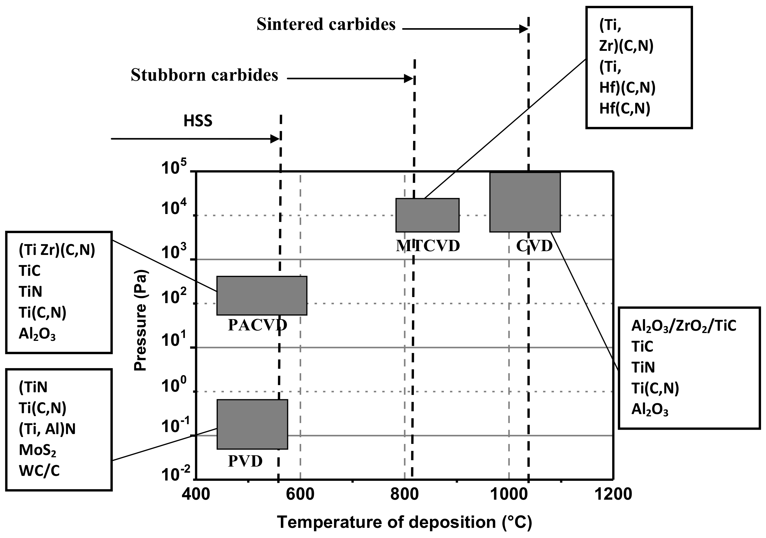
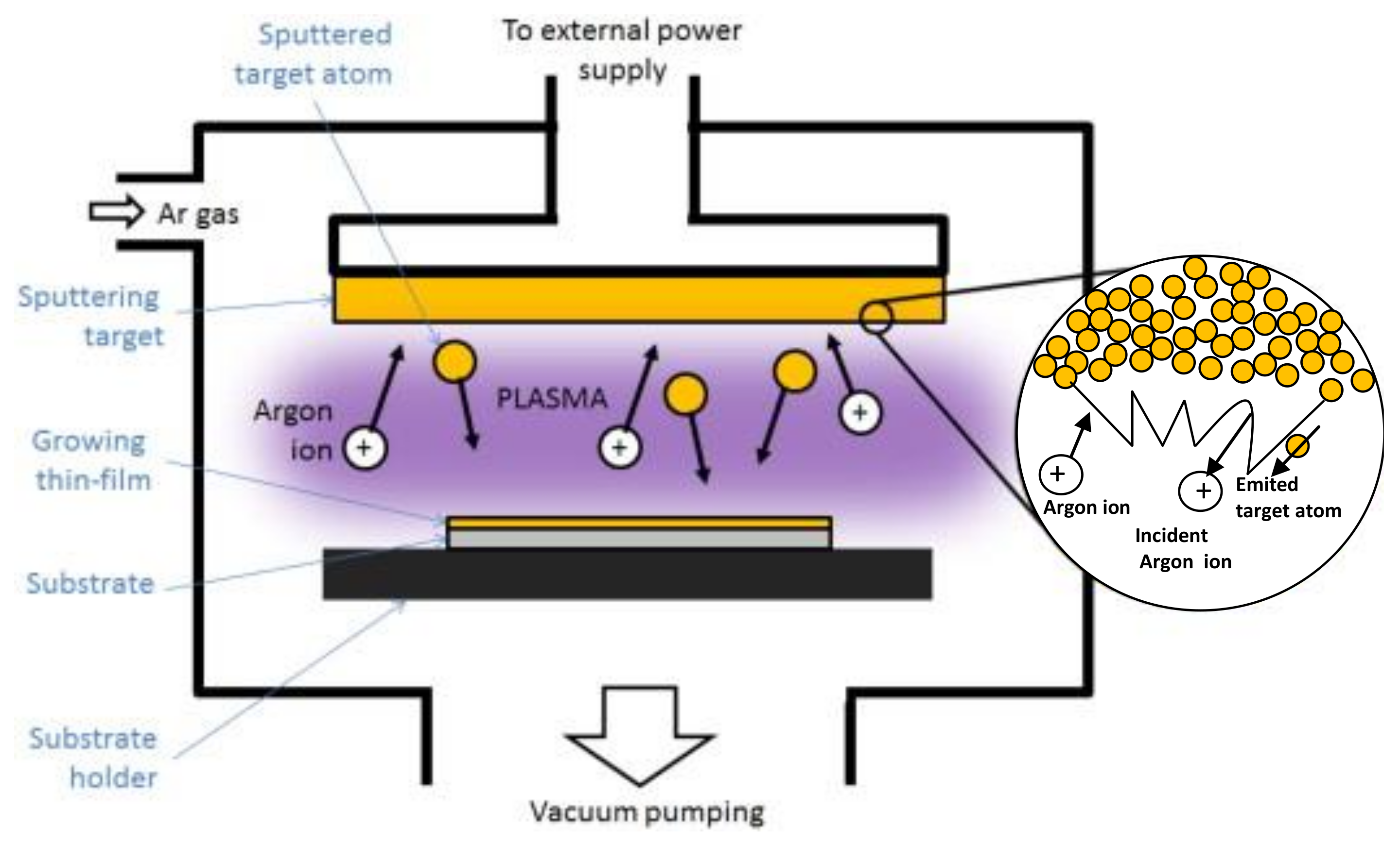
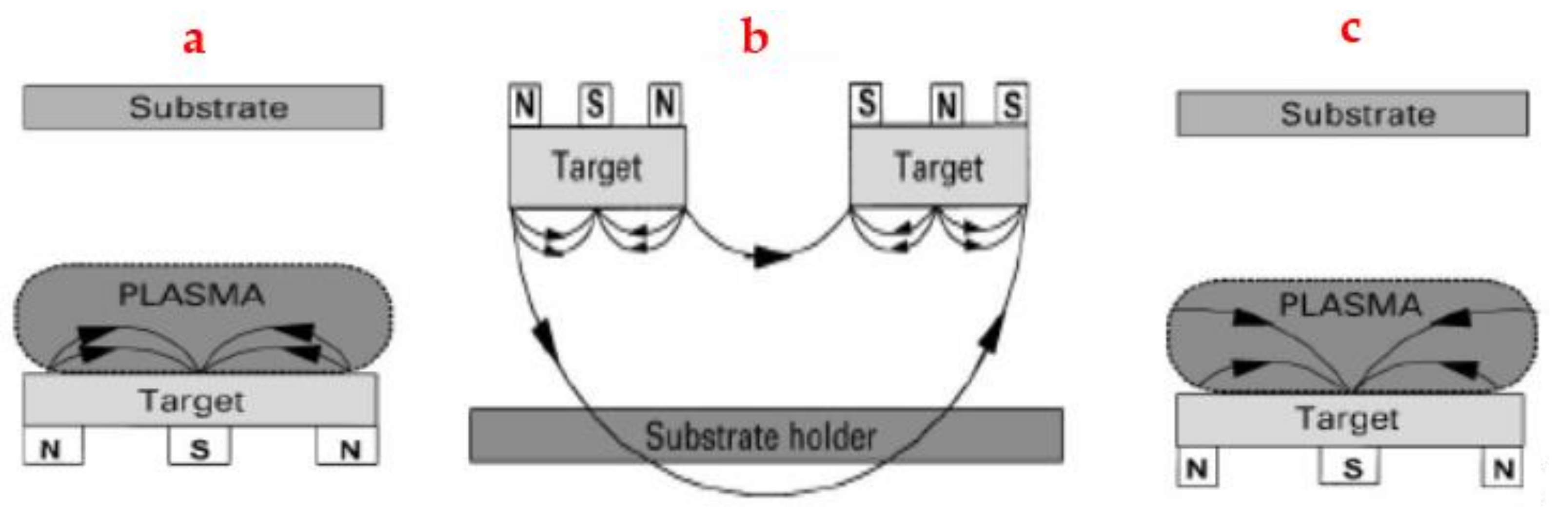
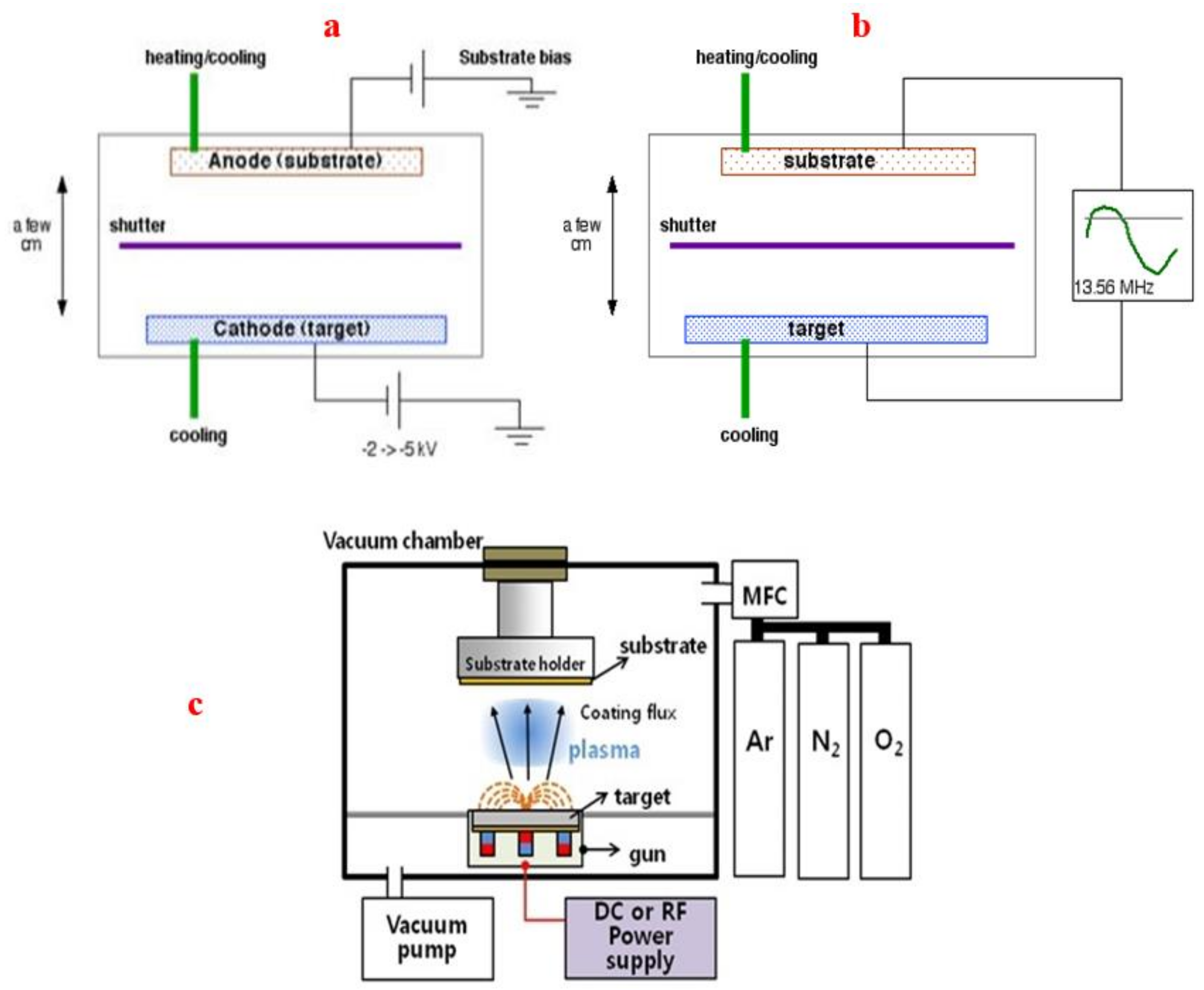
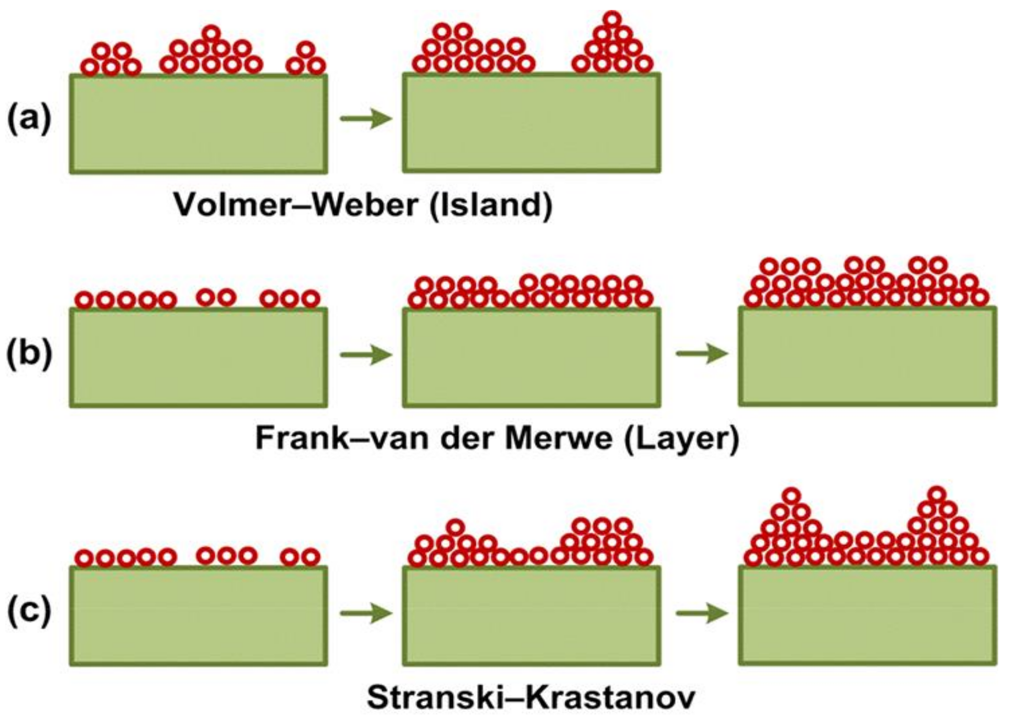
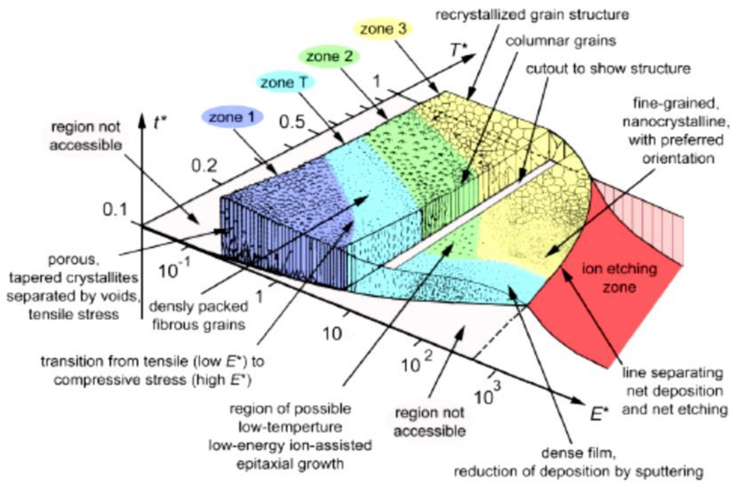
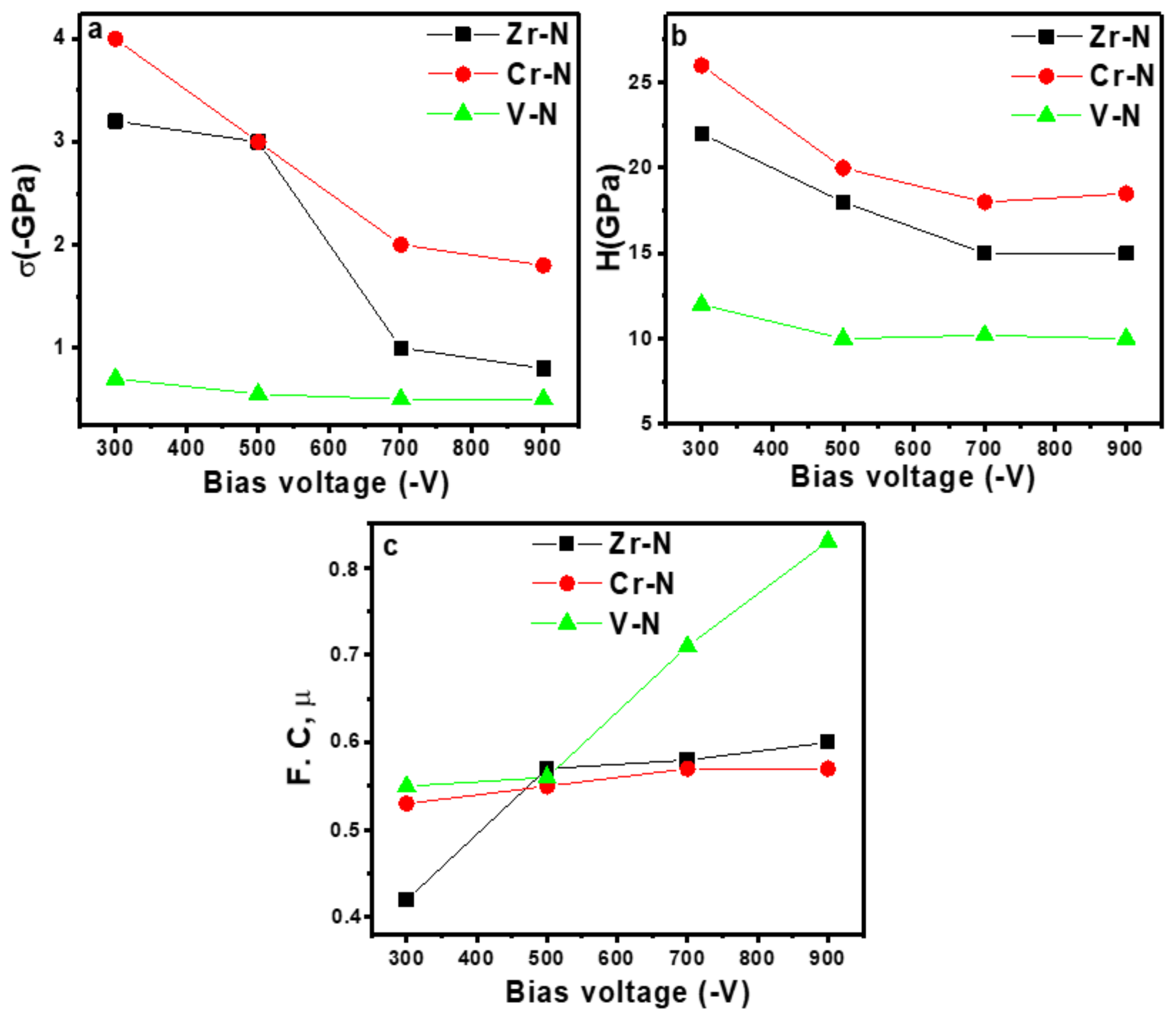
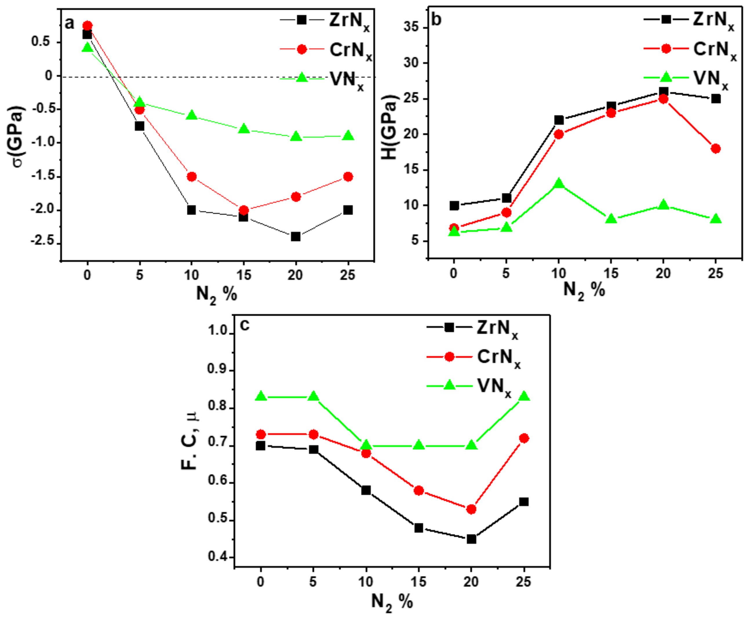
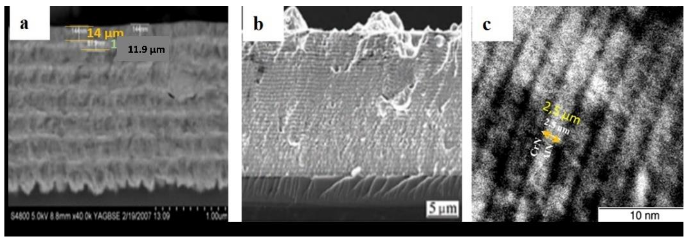
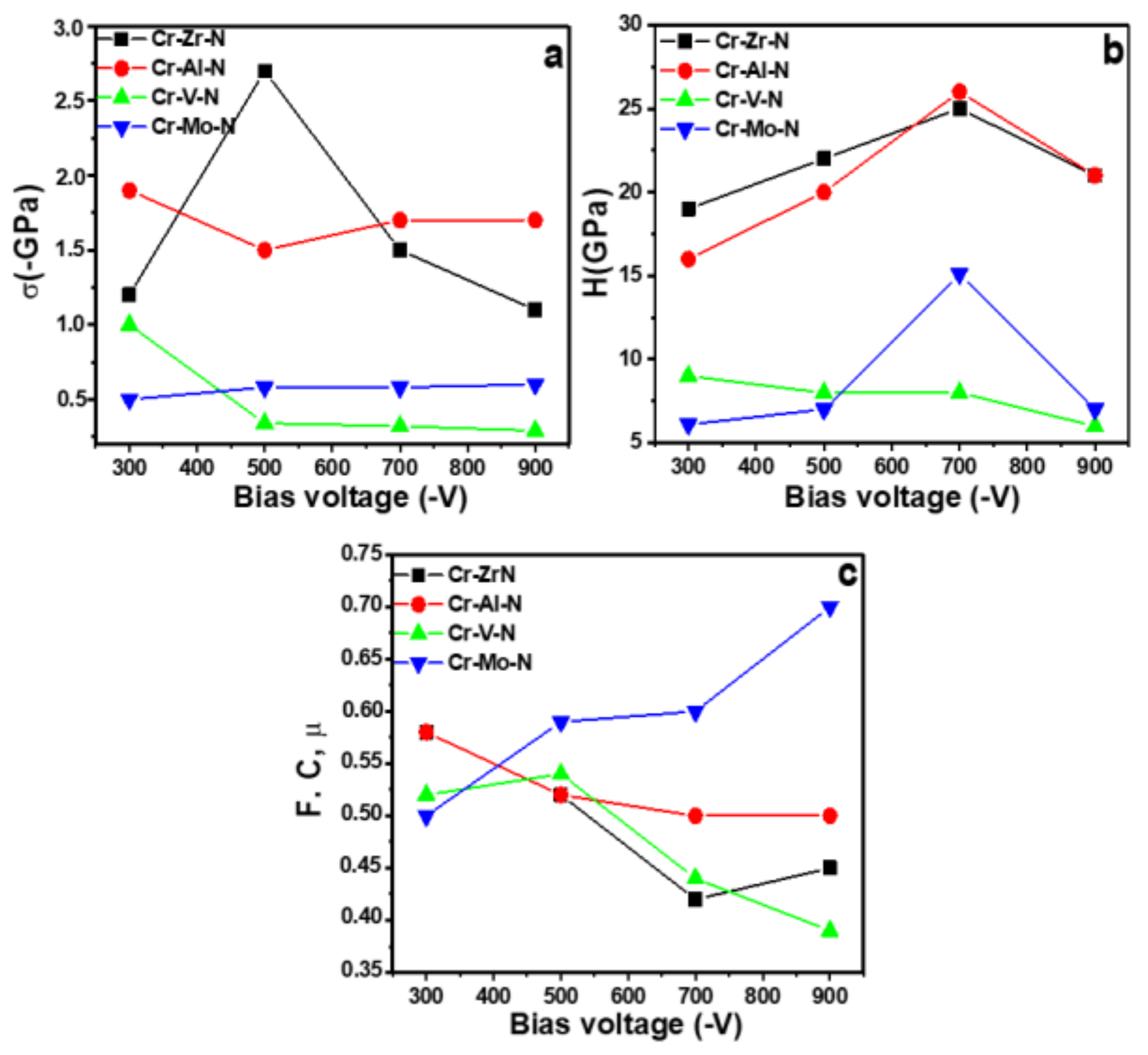
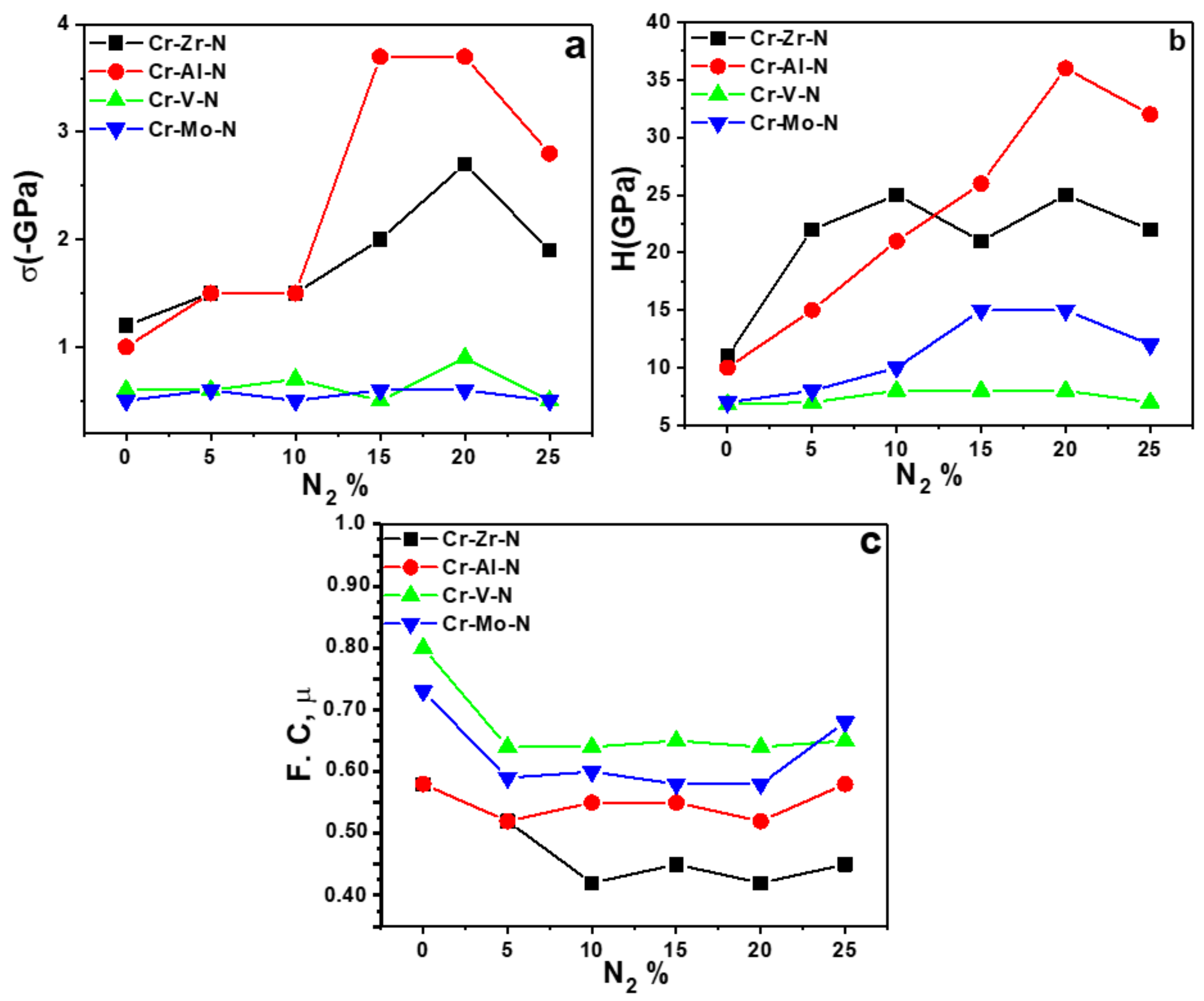
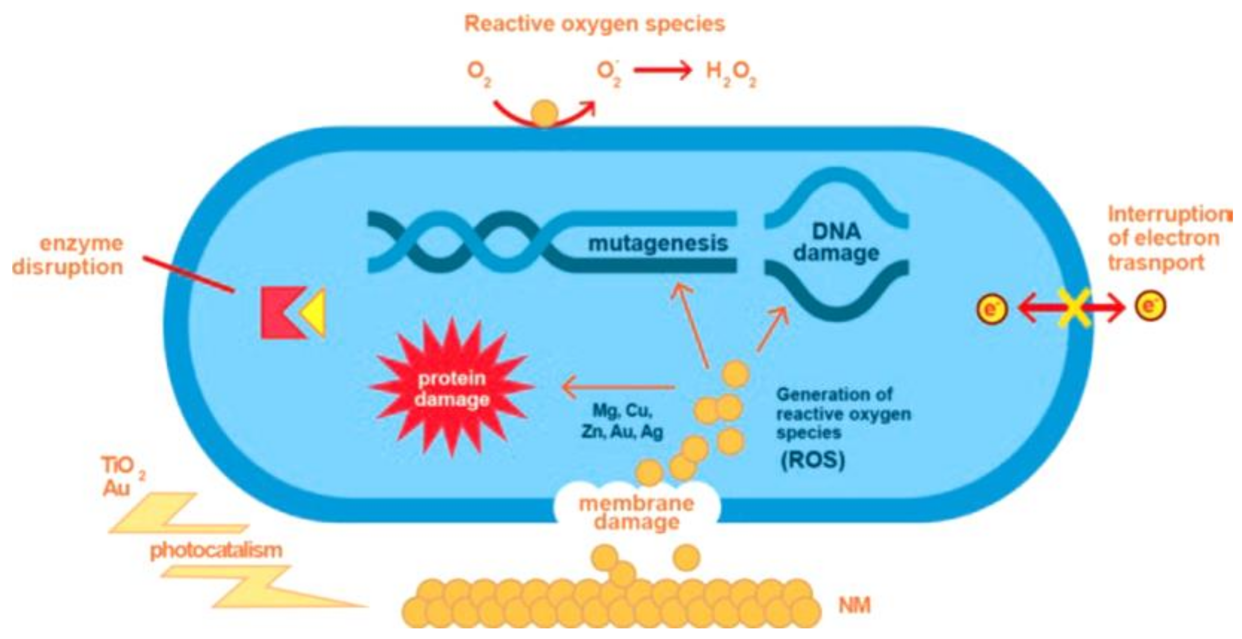
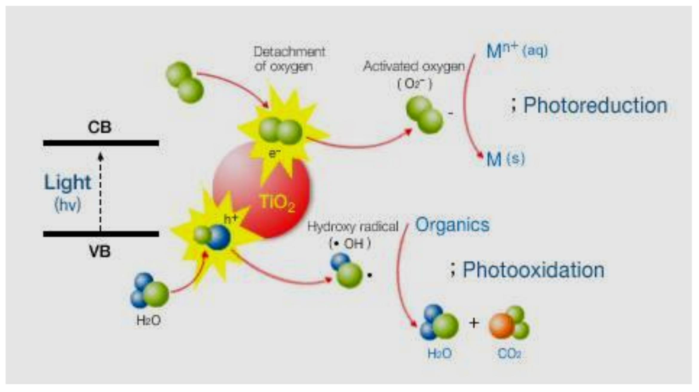
Table 1.
Some properties of binary transition metals thin films (TM).
| System | Conditions | Preferred Orientation | Hardness (GPa) | Young’s Modulus (GPa) | Ra (nm) | COF | Technique | Ref. | |
|---|---|---|---|---|---|---|---|---|---|
| TMN | TiN | Ar/N2 1:1 | (111) | - | - | 7.9 | 0.12 | DC magnetron sputtering | [2] |
| Ar+ N 6 cm3/min | - | up to 30 | up to 300 | 1.3 | - | DC reactive sputtering of a hot target | [3,39] | ||
| ZrN | 0.7 Pa | 111 | 16.022 | - | 11.20 | - | RF magnetron sputtering | [4,41] | |
| 50 V | 111 | 23.5 | - | - | - | DC magnetron sputtering system | [5] | ||
| CrN | 300 °C and 290 V | 200 | 21.2 | - | - | 4.97 | Pulsed DC reactive MS | [7] | |
| N2 flow rates 2–25 sccm substrate T° 303–973 K | 100 | 12 ± 1.81 | 250 ± 51.28 | 2 | 0.16 | Pulsed DC magnetron sputtering | [9] | ||
| TiO2 deposited on amorphous SiO2 using magnetron sputtering | 101 | 4.8 | - | - | - | Conventional magnetron sputtering | [11] | ||
| TiO2 deposited on Si substrates with modulated plasma MS | 110 | 16.1 | - | - | - | Plasma-modulated magnetron sputtering | [12] | ||
| ZrO | O2 flow rate 7.0–20.0 cm3 min−1; P(Ar) 0.3–1 Pa; P(O2) 0.04–0.15 Pa | 200 | 17.8 | 220 | 2.9 | - | DC reactive magnetron sputtering | [13] | |
| CrO | O2 flow rate 2.0–3.2 sccm with 0.3 sccm increments | 300 | 11–21 | - | - | - | Reactive magnetron sputtering | [18] | |
| TMB | TiBx | Bias −120 V and −50 V | 002 | 35.7 | 401.3 | 0.0158µm | - | Unbalanced magnetron sputtering | [36] |
| ZrB2 | Deposition times: 5 and 15 min | 001 | 45 | 350–400 | - | - | DC magnetron sputtering | [37] | |
| CrB2 | Different B/Cr ratios | 101 | 25 | - | - | 0.52–0.78 | Non-reactive DC magnetron sputtering | [38] | |
| TMC | TiC | Substrate bias −20 to −200 V | 111 | 28.8 | 302.5 | - | - | E303A magnetron sputtering | [39] |
| ZrC | Ts 25–290 °C | 111 | 30.2 | - | - | - | DC magnetron sputtering | [40] | |
| CrC | 0.4 Pa (700–100 °C) | 200 | 31 | 298 | - | 0.43 | RF magnetron sputtering | [35] |
Publisher’s Note: MDPI stays neutral with regard to jurisdictional claims in published maps and institutional affiliations. |
© 2022 by the authors. Licensee MDPI, Basel, Switzerland. This article is an open access article distributed under the terms and conditions of the Creative Commons Attribution (CC BY) license (https://creativecommons.org/licenses/by/4.0/).
Share and Cite
MDPI and ACS Style
Aissani, L.; Alhussein, A.; Zia, A.W.; Mamba, G.; Rtimi, S. Magnetron Sputtering of Transition Metal Nitride Thin Films for Environmental Remediation. Coatings 2022, 12, 1746. https://doi.org/10.3390/coatings12111746
AMA Style
Aissani L, Alhussein A, Zia AW, Mamba G, Rtimi S. Magnetron Sputtering of Transition Metal Nitride Thin Films for Environmental Remediation. Coatings. 2022; 12(11):1746. https://doi.org/10.3390/coatings12111746
Chicago/Turabian StyleAissani, Linda, Akram Alhussein, Abdul Wasy Zia, Gcina Mamba, and Sami Rtimi. 2022. "Magnetron Sputtering of Transition Metal Nitride Thin Films for Environmental Remediation" Coatings 12, no. 11: 1746. https://doi.org/10.3390/coatings12111746
Note that from the first issue of 2016, this journal uses article numbers instead of page numbers. See further details here.