Piezoelectric Micromachined Ultrasound Transducer Technology: Recent Advances and Applications


Abstract
:1. Introduction
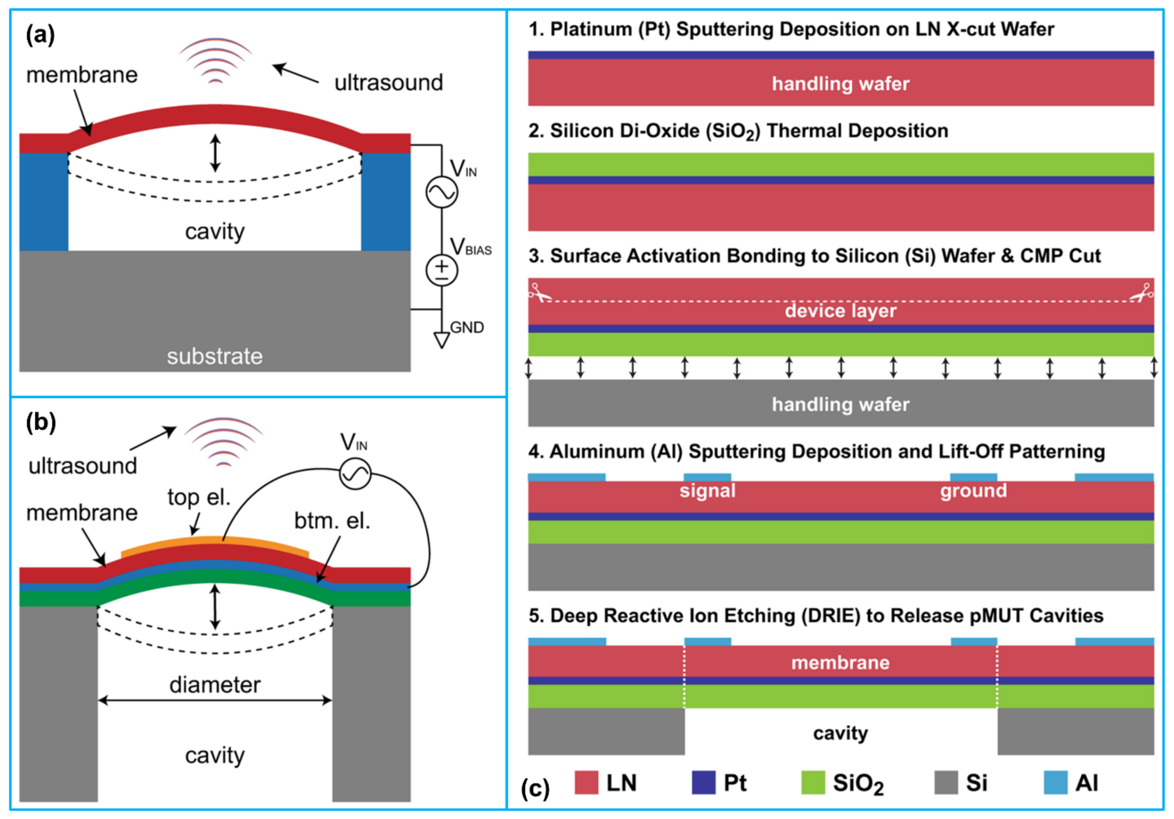
2. PMUT Structures
3. Materials and Fabrication Techniques
3.1. Piezoelectric Materials for PMUTs
3.1.1. Lead-Based Piezoelectric Thin Films
3.1.2. Lead-Free Piezoelectric Thin Films
AlN Thin Film
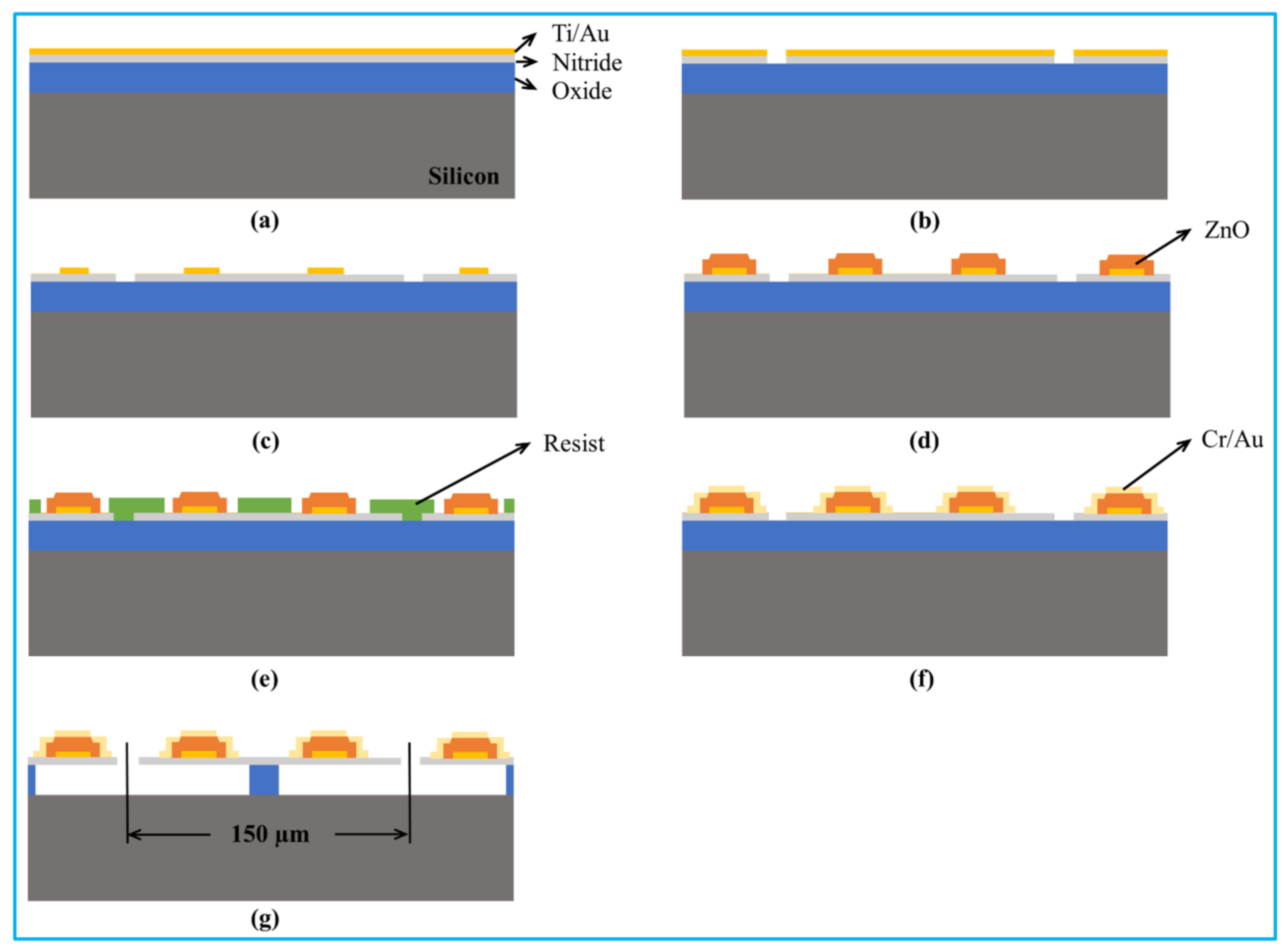
ZnO Thin film
3.2. Fabrication Techniques for PMUTs
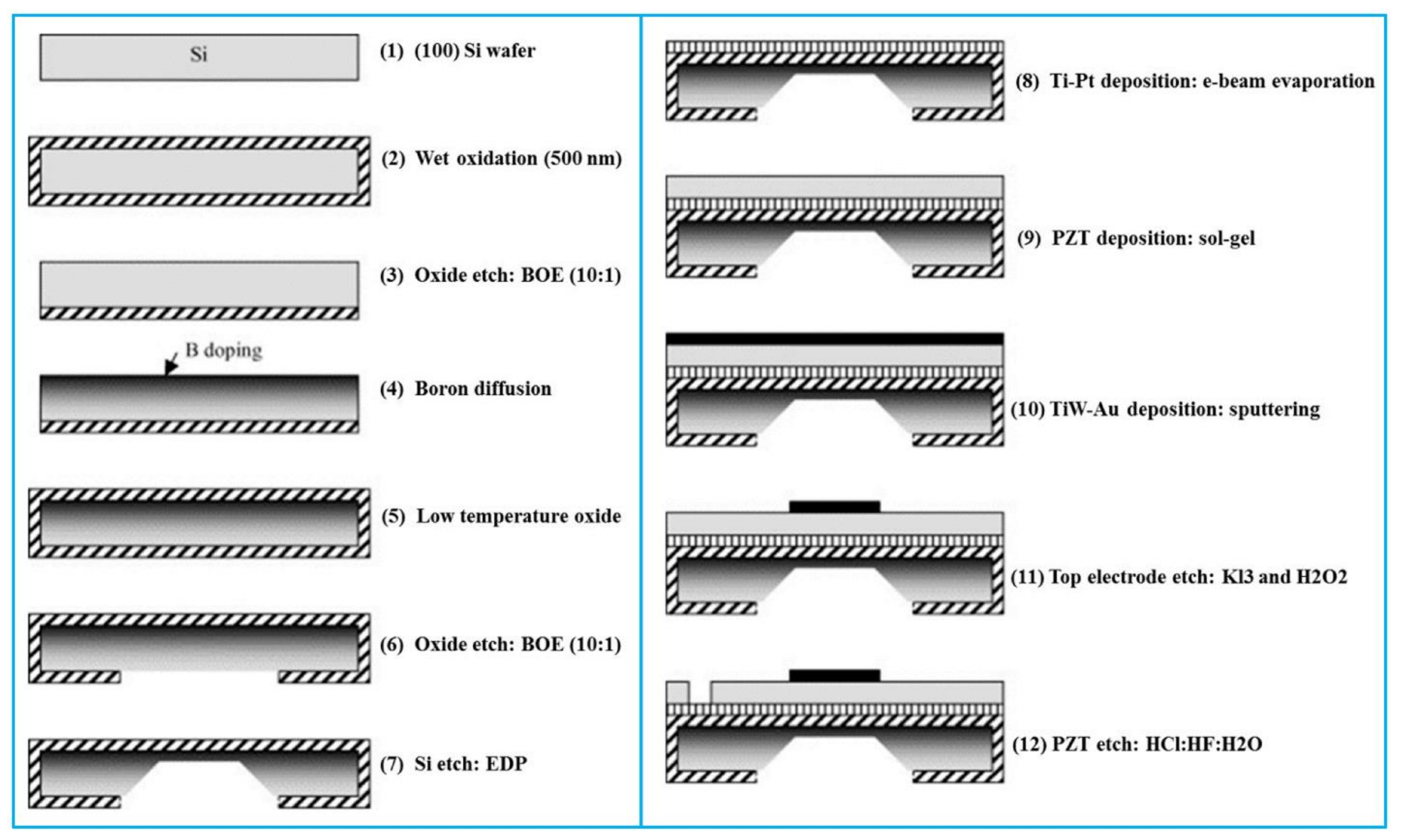
3.2.1. Frontside Etching
3.2.2. Backside Etching
3.2.3. Sacrificial Releasing
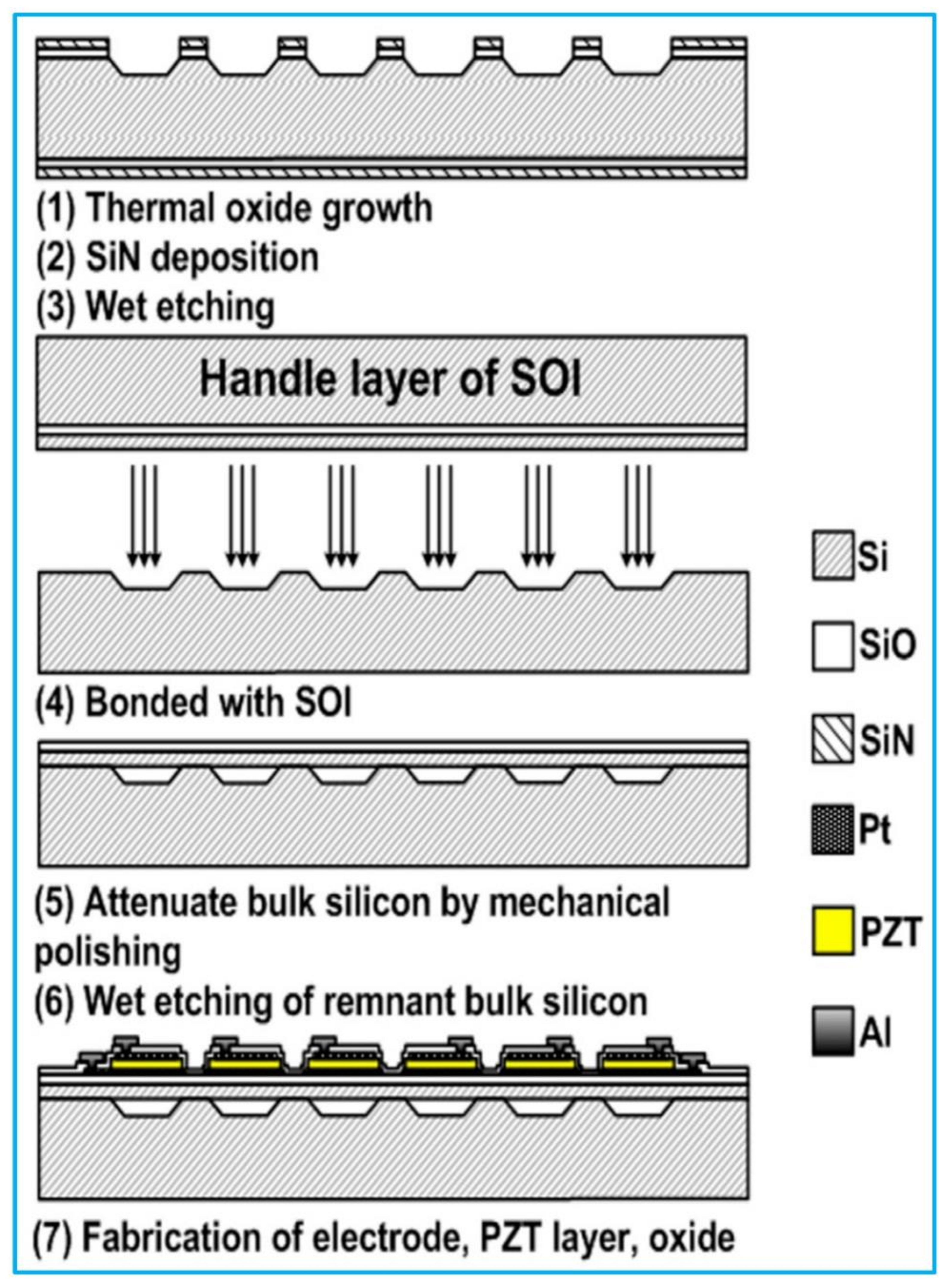
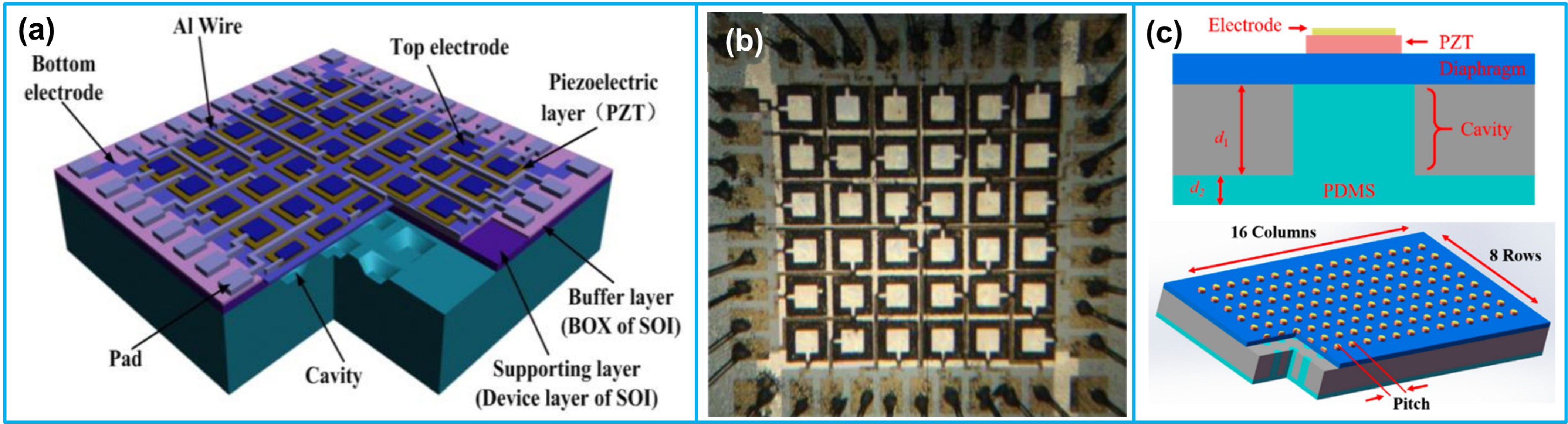
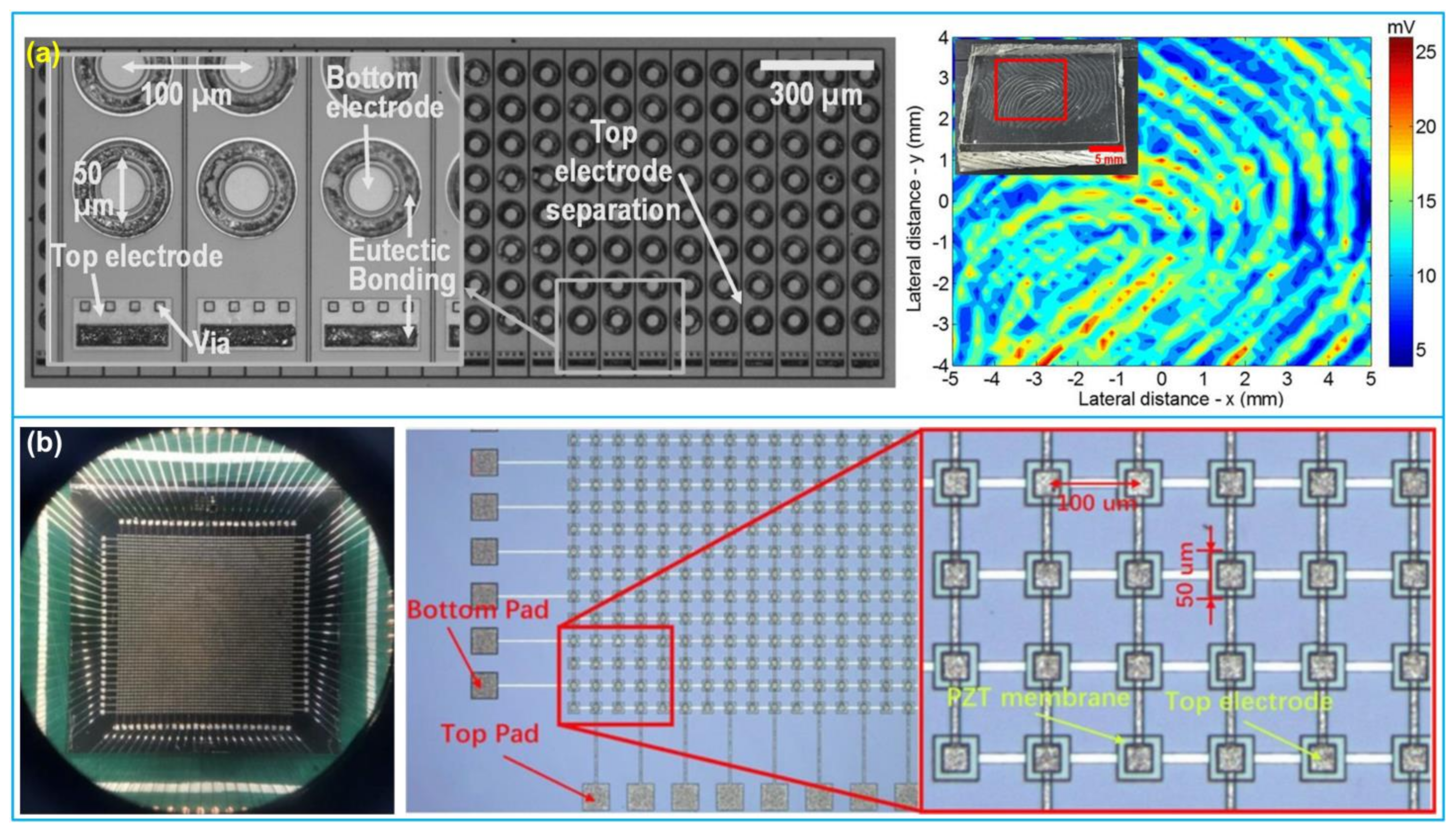
3.2.4. Cavity Wafer Bonding
4. Applications of PMUTs
4.1. Ultrasound Imaging
4.2. Photoacoustic Imaging
4.3. Fingerprint Sensing
4.4. Therapy
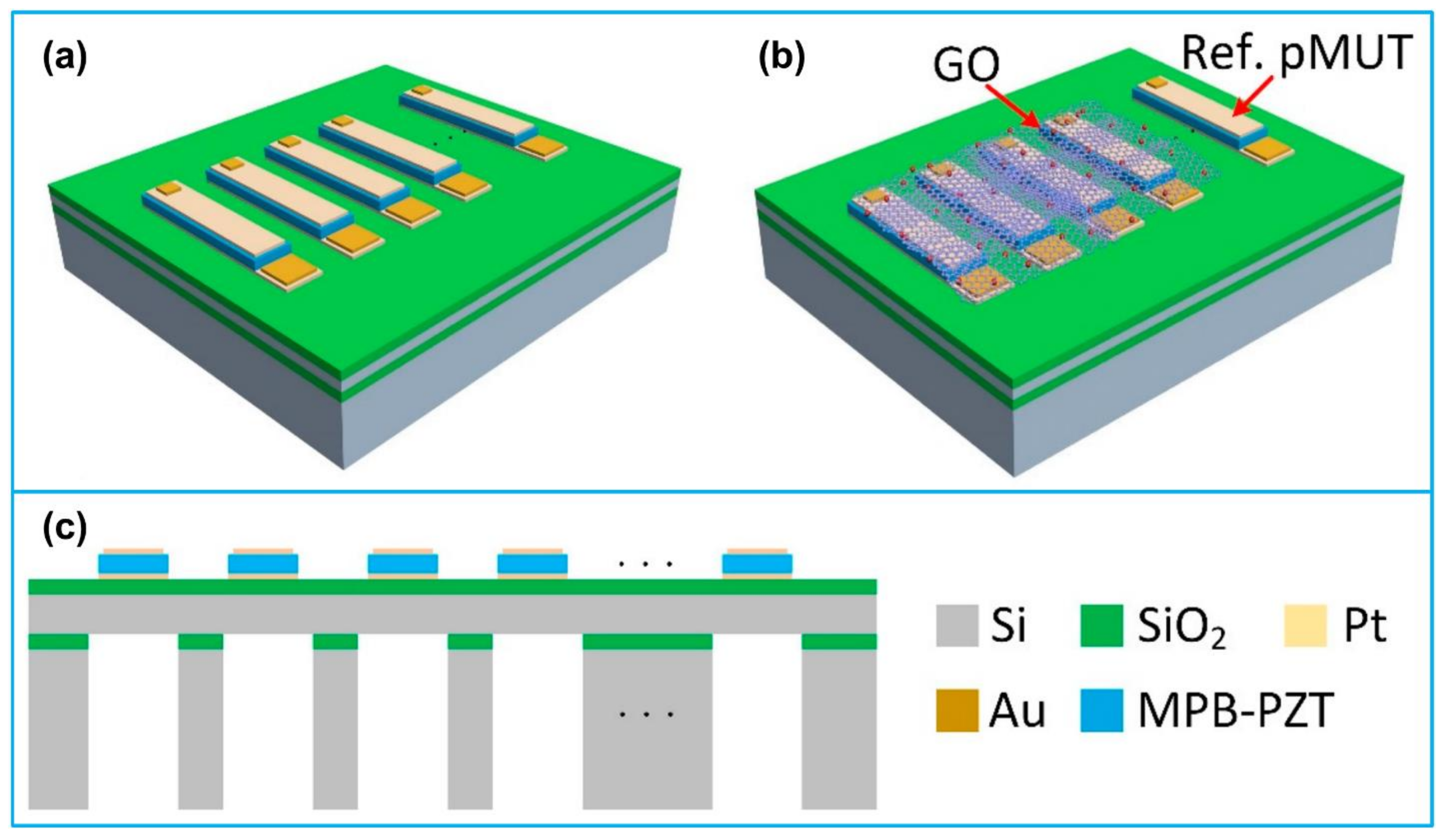
4.5. Chemical and Bio-Sensing
4.6. Physical Sensors
4.7. Airborne Applications
5. Conclusions and Future Perspectives
Author Contributions
Funding
Institutional Review Board Statement
Informed Consent Statement
Data Availability Statement
Conflicts of Interest
References
- Ter Haar, G.R. High Intensity Focused Ultrasound for the Treatment of Tumors. Echocardiography 2001, 18, 317–322. [Google Scholar] [CrossRef] [PubMed]
- Peng, C.; Chen, M.; Spicer, J.B.; Jiang, X. Acoustics at the Nanoscale (Nanoacoustics): A Comprehensive Literature Review. Part II: Nanoacoustics for Biomedical Imaging and Therapy. Sens. Actuators A Phys. 2021, 332, 112925. [Google Scholar] [CrossRef] [PubMed]
- Drinkwater, B.W.; Wilcox, P.D. Ultrasonic Arrays for Non-Destructive Evaluation: A Review. NDT e Int. 2006, 39, 525–541. [Google Scholar] [CrossRef]
- Jiang, X.; Kim, K.; Zhang, S.; Johnson, J.; Salazar, G. High-Temperature Piezoelectric Sensing. Sensors 2013, 14, 144–169. [Google Scholar] [CrossRef] [Green Version]
- Tang, H.-Y.; Lu, Y.; Jiang, X.; Ng, E.J.; Tsai, J.M.; Horsley, D.A.; Boser, B.E. 3-D Ultrasonic Fingerprint Sensor-on-a-Chip. IEEE J. Solid-State Circuits 2016, 51, 2522–2533. [Google Scholar] [CrossRef]
- Jiang, X.; Tang, H.-Y.; Lu, Y.; Ng, E.J.; Tsai, J.M.; Boser, B.E.; Horsley, D.A. Ultrasonic Fingerprint Sensor with Transmit Beamforming Based on a PMUT Array Bonded to CMOS Circuitry. IEEE Trans. Ultrason. Ferroelectr. Freq. Control 2017, 64, 1401–1408. [Google Scholar] [CrossRef]
- Peng, C.; Cai, Q.; Chen, M.; Jiang, X. Recent Advances in Tracking Devices for Biomedical Ultrasound Imaging Applications. Micromachines 2022, 13, 1855. [Google Scholar] [CrossRef]
- Tadigadapa, S.; Mateti, K. Piezoelectric MEMS Sensors: State-of-the-Art and Perspectives. Meas. Sci. Technol. 2009, 20, 92001. [Google Scholar] [CrossRef]
- Sammoura, F.; Akhbari, S.; Lin, L.; Kim, S.-G. Enhanced Coupling of Piezoelectric Micromachined Ultrasonic Transducers with Initial Static Deflection. In Proceedings of the SENSORS, 2013 IEEE, Baltimore, MD, USA, 3–6 November 2013; pp. 1–4. [Google Scholar]
- Zhou, Q.; Lau, S.; Wu, D.; Shung, K.K. Piezoelectric Films for High Frequency Ultrasonic Transducers in Biomedical Applications. Prog. Mater. Sci. 2011, 56, 139–174. [Google Scholar] [CrossRef] [Green Version]
- Fiering, J.O.; Hultman, P.; Lee, W.; Light, E.D.; Smith, S.W. High-Density Flexible Interconnect for Two-Dimensional Ultrasound Arrays. IEEE Trans. Ultrason. Ferroelectr. Freq. Control 2000, 47, 764–770. [Google Scholar] [CrossRef]
- Jung, J.; Lee, W.; Kang, W.; Shin, E.; Ryu, J.; Choi, H. Review of Piezoelectric Micromachined Ultrasonic Transducers and Their Applications. J. Micromechanics Microeng. 2017, 27, 113001. [Google Scholar] [CrossRef]
- Basij, M.; Yan, Y.; Alshahrani, S.S.; Helmi, H.; Burton, T.K.; Burmeister, J.W.; Dominello, M.M.; Winer, I.S.; Mehrmohammadi, M. Miniaturized Phased-Array Ultrasound and Photoacoustic Endoscopic Imaging System. Photoacoustics 2019, 15, 100139. [Google Scholar] [CrossRef] [PubMed]
- Wang, J.; Zheng, Z.; Chan, J.; Yeow, J.T.W. Capacitive Micromachined Ultrasound Transducers for Intravascular Ultrasound Imaging. Microsyst. Nanoeng. 2020, 6, 73. [Google Scholar] [CrossRef] [PubMed]
- Akhbari, S.; Sammoura, F.; Eovino, B.; Yang, C.; Lin, L. Bimorph Piezoelectric Micromachined Ultrasonic Transducers. J. Microelectromech. Syst. 2016, 25, 326–336. [Google Scholar] [CrossRef]
- Hajati, A.; Latev, D.; Gardner, D. 3D MEMS Piezoelectric Ultrasound Transducer Technology. In Proceedings of the 2013 Joint IEEE International Symposium on Applications of Ferroelectric and Workshop on Piezoresponse Force Microscopy (ISAF/PFM), Prague, Czech Republic, 21–25 July 2013; pp. 231–235. [Google Scholar]
- Lu, Y.; Heidari, A.; Shelton, S.; Guedes, A.; Horsley, D.A. High Frequency Piezoelectric Micromachined Ultrasonic Transducer Array for Intravascular Ultrasound Imaging. In Proceedings of the 2014 IEEE 27th International Conference on Micro Electro Mechanical Systems (MEMS), San Francisco, CA, USA, 26–28 January 2014; pp. 745–748. [Google Scholar]
- Jiang, X.; Lu, Y.; Tang, H.-Y.; Tsai, J.M.; Ng, E.J.; Daneman, M.J.; Boser, B.E.; Horsley, D.A. Monolithic Ultrasound Fingerprint Sensor. Microsyst. Nanoeng. 2017, 3, 17059. [Google Scholar] [CrossRef] [PubMed] [Green Version]
- Wang, H.; Chen, Z.; Yang, H.; Jiang, H.; Xie, H. A Ceramic PZT-Based PMUT Array for Endoscopic Photoacoustic Imaging. J. Microelectromech. Syst. 2020, 29, 1038–1043. [Google Scholar] [CrossRef] [PubMed]
- Qiu, Y.; Gigliotti, J.V.; Wallace, M.; Griggio, F.; Demore, C.E.M.; Cochran, S.; Trolier-McKinstry, S. Piezoelectric Micromachined Ultrasound Transducer (PMUT) Arrays for Integrated Sensing, Actuation and Imaging. Sensors 2015, 15, 8020–8041. [Google Scholar] [CrossRef] [Green Version]
- Lee, C.; Kim, J.Y.; Kim, C. Recent Progress on Photoacoustic Imaging Enhanced with Microelectromechanical Systems (MEMS) Technologies. Micromachines 2018, 9, 584. [Google Scholar] [CrossRef] [Green Version]
- Peng, C.; Wu, H.; Kim, S.; Dai, X.; Jiang, X. Recent Advances in Transducers for Intravascular Ultrasound (IVUS) Imaging. Sensors 2021, 21, 3540. [Google Scholar] [CrossRef]
- Qualcomm Qualcomm Ultrasonic Fingerprint Sensor. Available online: https://www.qualcomm.com/videos/qualcomm-ultrasonic-fingerprint-sensor (accessed on 14 November 2022).
- Muralt, P.; Ledermann, N.; Paborowski, J.; Barzegar, A.; Gentil, S.; Belgacem, B.; Petitgrand, S.; Bosseboeuf, A.; Setter, N. Piezoelectric Micromachined Ultrasonic Transducers Based on PZT Thin Films. IEEE Trans. Ultrason. Ferroelectr. Freq. Control 2005, 52, 2276–2288. [Google Scholar] [CrossRef]
- Kazari, H.; Kabir, M.; Mostavi, A.; Ozevin, D. Multi-Frequency Piezoelectric Micromachined Ultrasonic Transducers. IEEE Sens. J. 2019, 19, 11090–11099. [Google Scholar] [CrossRef]
- Pop, F.; Herrera, B.; Rinaldi, M. Lithium Niobate Piezoelectric Micromachined Ultrasonic Transducers for High Data-Rate Intrabody Communication. Nat. Commun. 2022, 13, 1782. [Google Scholar] [CrossRef] [PubMed]
- Muralt, P.; Baborowski, J. Micromachined Ultrasonic Transducers and Acoustic Sensors Based on Piezoelectric Thin Films. J. electroceram. 2004, 12, 101–108. [Google Scholar] [CrossRef]
- Yuan, J.; Rhee, S.; Jiang, X.N. 60 MHz PMN-PT Based 1-3 Composite Transducer for IVUS Imaging. In Proceedings of the 2008 IEEE Ultrasonics Symposium, Beijing, China, 2–5 November 2008; pp. 682–685. [Google Scholar]
- Jiang, X.; Snook, K.; Cheng, A.; Hackenberger, W.S.; Geng, X. Micromachined PMN-PT Single Crystal Composite Transducers--15–75 MHz PC-MUT. In Proceedings of the 2008 IEEE Ultrasonics Symposium, Beijing, China, 2–5 November 2008; pp. 164–167. [Google Scholar]
- Kang, W.; Jung, J.; Lee, W.; Ryu, J.; Choi, H. A Thickness-Mode Piezoelectric Micromachined Ultrasound Transducer Annular Array Using a PMN–PZT Single Crystal. J. Micromech. Microeng. 2018, 28, 75015. [Google Scholar] [CrossRef]
- Akasheh, F.; Fraser, J.D.; Bose, S.; Bandyopadhyay, A. Piezoelectric Micromachined Ultrasonic Transducers: Modeling the Influence of Structural Parameters on Device Performance. IEEE Trans. Ultrason. Ferroelectr. Freq. Control 2005, 52, 455–468. [Google Scholar] [CrossRef]
- Bhargav, G.; Sharma, A. Design, Simulation and Optimization of Circular, Square and Hexagonal Shaped Diaphragms for PMUT Application. In Micro and Nanoelectronics Devices, Circuits and Systems; Springer: Berlin/Heidelberg, Germany, 2021; pp. 467–476. [Google Scholar]
- Yu, Q.; Fan, G.; Ren, W.; Fan, Q.; Ti, J.; Li, J.; Wang, C. PZT-Film-Based Piezoelectric Micromachined Ultrasonic Transducer with I-Shaped Composite Diaphragm. Micromachines 2022, 13, 1597. [Google Scholar] [CrossRef]
- Eovino, B.E.; Akhbari, S.; Lin, L. Ring Shaped Piezoelectric Micromachined Ultrasonic Transducers (PMUT) with Increased Pressure Generation. In Proceedings of the Solid-State Sensors, Actuators Microsystems Workshop, Hilton Head Island, SC, USA, 5–9 June 2016; pp. 5–9. [Google Scholar]
- Thao, P.N.; Yoshida, S.; Tanaka, S. Development of Mechanically-Robust Piezoelectric Micromachined Ultrasonic Transducer Based on Island-Shaped Monocrystalline PZT Thin Film Partially Covered with Polyimide. J. Micromech. Microeng. 2020, 30, 125015. [Google Scholar] [CrossRef]
- Liu, Z.; Yoshida, S.; Tanaka, S. Fabrication and Characterization of Annular-Shaped Piezoelectric Micromachined Ultrasonic Transducer Mounted with Pb (Zr, Ti) O3-Based Monocrystalline Thin Film. J. Micromech. Microeng. 2021, 31, 125014. [Google Scholar] [CrossRef]
- Li, P.; Fan, Z.; Duan, X.; Cui, D.; Zang, J.; Zhang, Z.; Xue, C. Enhancement of the Transmission Performance of Piezoelectric Micromachined Ultrasound Transducers by Vibration Mode Optimization. Micromachines 2022, 13, 596. [Google Scholar] [CrossRef]
- Akhbari, S.; Sammoura, F.; Yang, C.; Heidari, A.; Horsley, D.; Lin, L. Self-Curved Diaphragms by Stress Engineering for Highly Responsive PMUT. In Proceedings of the 2015 28th IEEE International Conference on Micro Electro Mechanical Systems (MEMS), Estoril, Portugal, 18–22 January 2015; pp. 837–840. [Google Scholar]
- Wang, T.; Sawada, R.; Lee, C. A Piezoelectric Micromachined Ultrasonic Transducer Using Piston-like Membrane Motion. IEEE Electron Device Lett. 2015, 36, 957–959. [Google Scholar] [CrossRef]
- Wang, M.; Zhou, Y. Design of Piezoelectric Micromachined Ultrasonic Transducers (PMUTs) for High Pressure Output. Microsyst. Technol. 2017, 23, 1761–1766. [Google Scholar] [CrossRef]
- Zhang, S.; Li, F.; Luo, J.; Sahul, R.; Shrout, T.R. Relaxor-PbTiO3 Single Crystals for Various Applications. IEEE Trans. Ultrason. Ferroelectr. Freq. Control 2013, 60, 1572–1580. [Google Scholar] [CrossRef] [PubMed] [Green Version]
- Sun, E.; Cao, W. Relaxor-Based Ferroelectric Single Crystals: Growth, Domain Engineering, Characterization and Applications. Prog. Mater. Sci. 2014, 65, 124–210. [Google Scholar] [CrossRef] [PubMed] [Green Version]
- Zhang, S.; Li, F.; Jiang, X.; Kim, J.; Luo, J.; Geng, X. Advantages and Challenges of Relaxor-PbTiO3 Ferroelectric Crystals for Electroacoustic Transducers—A Review. Prog. Mater. Sci. 2015, 68, 1–66. [Google Scholar] [CrossRef] [Green Version]
- Zhang, S.; Li, F.; Yu, F.; Jiang, X.; Lee, H.-Y.; Luo, J.; Shrout, T.R. Recent Developments in Piezoelectric Crystals. J. Korean Ceram. Soc. 2018, 55, 419–439. [Google Scholar] [CrossRef] [Green Version]
- Yamashita, Y.; Karaki, T.; Lee, H.-Y.; Wan, H.; Kim, H.-P.; Jiang, X. A Review of Lead Perovskite Piezoelectric Single Crystals and Their Medical Transducers Application. IEEE Trans. Ultrason. Ferroelectr. Freq. Control 2022, 69, 3048–3056. [Google Scholar] [CrossRef] [PubMed]
- Wang, Z.; Miao, J.; Zhu, W. Piezoelectric Thick Films and Their Application in MEMS. J. Eur. Ceram. Soc. 2007, 27, 3759–3764. [Google Scholar] [CrossRef]
- Matsushima, T.; Xiong, S.; Kawada, H.; Yamanaka, H.; Muralt, P. A Highly Sensitive Pb (Zr, Ti)O3 Thin Film Ultrasonic Micro-Sensor with a Grooved Diaphragm. IEEE Trans. Ultrason. Ferroelectr. Freq. Control 2007, 54, 2439–2445. [Google Scholar] [CrossRef]
- Jung, J.; Kim, S.; Lee, W.; Choi, H. Fabrication of a Two-Dimensional Piezoelectric Micromachined Ultrasonic Transducer Array Using a Top-Crossover-to-Bottom Structure and Metal Bridge Connections. J. Micromech. Microeng. 2013, 23, 125037. [Google Scholar] [CrossRef]
- Wang, T.; Kobayashi, T.; Lee, C. Micromachined Piezoelectric Ultrasonic Transducer with Ultra-Wide Frequency Bandwidth. Appl. Phys. Lett. 2015, 106, 13501. [Google Scholar] [CrossRef]
- Woodward, D.I.; Knudsen, J.; Reaney, I.M. Review of Crystal and Domain Structures in the PbZrxTi1−xO3 Solid Solution. Phys. Rev. B 2005, 72, 104110. [Google Scholar] [CrossRef]
- Lee, C.; Kawano, S.; Itoh, T.; Suga, T. Characteristics of Sol-Gel Derived PZT Thin Films with Lead Oxide Cover Layers and Lead Titanate Interlayers. J. Mater. Sci. 1996, 31, 4559–4568. [Google Scholar] [CrossRef]
- Muralt, P. PZT Thin Films for Microsensors and Actuators: Where Do We Stand? IEEE Trans. Ultrason. Ferroelectr. Freq. Control 2000, 47, 903–915. [Google Scholar] [CrossRef] [PubMed]
- Gablech, I.; Svatoš, V.; Caha, O.; Hrabovský, M.; Prášek, J.; Hubálek, J.; Šikola, T. Preparation of (001) Preferentially Oriented Titanium Thin Films by Ion-Beam Sputtering Deposition on Thermal Silicon Dioxide. J. Mater. Sci. 2016, 51, 3329–3336. [Google Scholar] [CrossRef] [Green Version]
- Mahdi, M.; Kadri, M. Effect of KrF Laser Irradiation on the Morphology and Microstructure of Amorphous PZT Thin Films Grown by RF Magnetron Sputtering. J. Electron. Mater. 2021, 50, 4450–4455. [Google Scholar] [CrossRef]
- Lin, Y.C.; Chuang, H.A.; Shen, J.H. PZT Thin Film Preparation by Pulsed DC Magnetron Sputtering. Vacuum 2009, 83, 921–926. [Google Scholar] [CrossRef]
- Otani, Y.; Okamura, S.; Shiosaki, T. Recent Developments on MOCVD of Ferroelectric Thin Films. J. Electroceram. 2004, 13, 15–22. [Google Scholar] [CrossRef]
- Cheng, J.; Meng, Z. Thickness-Dependent Microstructures and Electrical Properties of PZT Films Derived from Sol-Gel Process. Thin Solid Films 2001, 385, 5–10. [Google Scholar] [CrossRef]
- Wang, Y.; Santiago-Avilés, J.J. Synthesis of Lead Zirconate Titanate Nanofibres and the Fourier-Transform Infrared Characterization of Their Metallo-Organic Decomposition Process. Nanotechnology 2003, 15, 32. [Google Scholar] [CrossRef]
- Lee, J.; Safari, A.; Pfeffer, R.L. Growth of Epitaxial Pb(Zr,Ti)O3 Films by Pulsed Laser Deposition. Appl. Phys. Lett. 1992, 61, 1643–1645. [Google Scholar] [CrossRef]
- Wang, Z.J.; Karibe, I.; Maeda, R.; Kokawa, H. Preparation of Lead Zirconate Titanate Thin Films Derived by Hybrid Processing: Sol-gel Method and Laser Ablation. J. Am. Ceram. Soc. 2002, 85, 3108–3110. [Google Scholar] [CrossRef]
- Krebs, H.-U.; Weisheit, M.; Faupel, J.; Süske, E.; Scharf, T.; Fuhse, C.; Störmer, M.; Sturm, K.; Seibt, M.; Kijewski, H. Pulsed Laser Deposition (PLD)—A Versatile Thin Film Technique. Adv. Solid State Phys. 2003, 43, 505–518. [Google Scholar]
- Chen, K.C.; Mackenzie, J.D. Crystallization Kinetics of Metallo-Organics Derived PZT Thin Film. MRS Online Proc. Libr. 1990, 180, 663. [Google Scholar] [CrossRef]
- Calame, F.; Muralt, P. Growth and Properties of Gradient Free Sol-Gel Lead Zirconate Titanate Thin Films. Appl. Phys. Lett. 2007, 90, 62907. [Google Scholar] [CrossRef]
- Chen, Y.-Q.; Li, Y.-X.; Chen, Y.; Ju, Z.-Y.; Tao, L.-Q.; Pang, Y.; Yang, Y.; Ren, T. Large-Scale and High-Density PMUT Array Based on Isolated Sol-Gel PZT Membranes for Fingerprint Imaging. J. Electrochem. Soc. 2017, 164, B377–B381. [Google Scholar] [CrossRef] [Green Version]
- Klein, L.C. Sol-Gel Optics: Processing and Applications; Springer Science & Business Media: Berlin, Germany, 2013; p. 599. ISBN 1461527503. [Google Scholar]
- Izyumskaya, N.; Alivov, Y.-I.; Cho, S.-J.; Morkoç, H.; Lee, H.; Kang, Y.-S. Processing, Structure, Properties, and Applications of PZT Thin Films. Crit. Rev. Solid state Mater. Sci. 2007, 32, 111–202. [Google Scholar] [CrossRef]
- Lim, U.-H.; Yoo, J.-H.; Kondalkar, V.; Lee, K. Development of High Frequency PMUT Based on Sputtered PZT. J. Electr. Eng. Technol. 2018, 13, 2434–2440. [Google Scholar]
- Matsuoka, T.; Kozuka, H.; Kitamura, K.; Yamada, H.; Kurahashi, T.; Yamazaki, M.; Ohbayashi, K. KNN–NTK Composite Lead-Free Piezoelectric Ceramic. J. Appl. Phys. 2014, 116, 154104. [Google Scholar] [CrossRef]
- Yang, J.; Zhang, F.; Yang, Q.; Liu, Z.; Li, Y.; Liu, Y.; Zhang, Q. Large Piezoelectric Properties in KNN-Based Lead-Free Single Crystals Grown by a Seed-Free Solid-State Crystal Growth Method. Appl. Phys. Lett. 2016, 108, 182904. [Google Scholar] [CrossRef] [Green Version]
- Mallik, H.S.; Fujii, I.; Matsui, Y.; Khanal, G.P.; Kim, S.; Ueno, S.; Suzuki, T.S.; Wada, S. Preparation and Investigation of Hexagonal-Tetragonal BaTiO3 Powders. J. Ceram. Soc. Japan 2021, 129, 91–96. [Google Scholar] [CrossRef]
- Sapkota, P.; Fujii, I.; Kim, S.; Ueno, S.; Moriyoshi, C.; Kuroiwa, Y.; Wada, S. Mn–Nb Co-Doping in Barium Titanate Ceramics by Different Solid-State Reaction Routes for Temperature Stable and DC-Bias Free Dielectrics. Ceram. Int. 2022, 48, 2154–2160. [Google Scholar] [CrossRef]
- Lee, M.H.; Park, J.S.; Kim, D.J.; Kambale, R.C.; Kim, M.-H.; Song, T.K.; Jung, H.J.; Kim, S.W.; Choi, H.I.; Kim, W.-J. Ferroelectric and Piezoelectric Properties of BiFeO3-BaTiO3Solid Solution Ceramics. Ferroelectrics 2013, 452, 7–12. [Google Scholar] [CrossRef]
- Khanal, G.P.; Fujii, I.; Kim, S.; Ueno, S.; Wada, S. Fabrication of (Bi0.5K0.5)TiO3 Modified BaTiO3-Bi (Mg0.5Ti0.5) O3-BiFeO3 Piezoelectric Ceramics. J. Eur. Ceram. Soc. 2021, 41, 4108–4115. [Google Scholar] [CrossRef]
- Kim, S.; Choi, H.; Han, S.; Park, J.S.; Lee, M.H.; Song, T.K.; Kim, M.-H.; Do, D.; Kim, W.-J. A Correlation between Piezoelectric Response and Crystallographic Structural Parameter Observed in Lead-Free (1−x)(Bi0.5Na0.5) TiO3–XSrTiO3 Piezoelectrics. J. Eur. Ceram. Soc. 2017, 37, 1379–1386. [Google Scholar] [CrossRef]
- Zhou, X.; Qi, H.; Yan, Z.; Xue, G.; Luo, H.; Zhang, D. Superior Thermal Stability of High Energy Density and Power Density in Domain-Engineered Bi0.5Na0.5TiO3–NaTaO3 Relaxor Ferroelectrics. ACS Appl. Mater. Interfaces 2019, 11, 43107–43115. [Google Scholar] [CrossRef]
- Hussain, A.; Zheng, P.; Xu, X.; Chen, X.; Li, T.; Wang, Y.; Yuan, G.; Yin, J.; Liu, Z. Structural and Electrical Properties of Multiferroic (1−x) BiFeO3−XBi0.5K0.5TiO3 Ceramics. J. Alloys Compd. 2016, 678, 228–233. [Google Scholar] [CrossRef]
- Lin, P.; Fei, C.; Hou, S.; Zhao, T.; Chen, Q.; Quan, Y.; Shung, K.K.; Zhou, Q. 0.36 BiScO3–0.64 PbTiO3/Epoxy 1–3 Composite for Ultrasonic Transducer Applications. IEEE Sens. J. 2018, 18, 5685–5690. [Google Scholar] [CrossRef]
- Dong, Y.; Zou, K.; Liang, R.; Zhou, Z. Review of BiScO3-PbTiO3 Piezoelectric Materials for High Temperature Applications: Fundamental, Progress, and Perspective. Prog. Mater. Sci. 2022, 132, 101026. [Google Scholar] [CrossRef]
- Galsin, J.S. Crystal Structure of Solids. Solid State Phys. 2019, 13, 1–36. [Google Scholar]
- Trolier-McKinstry, S.; Muralt, P. Thin Film Piezoelectrics for MEMS. J. Electroceram. 2004, 12, 7–17. [Google Scholar] [CrossRef]
- Guedes, A.; Shelton, S.; Przybyla, R.; Izyumin, I.; Boser, B.; Horsley, D.A. Aluminum Nitride PMUT Based on a Flexurally-Suspended Membrane. In Proceedings of the 2011 16th International Solid-State Sensors, Actuators and Microsystems Conference, Beijing, China, 5–9 June 2011; pp. 2062–2065. [Google Scholar]
- Piazza, G.; Felmetsger, V.; Muralt, P.; Olsson III, R.H.; Ruby, R. Piezoelectric Aluminum Nitride Thin Films for Microelectromechanical Systems. MRS Bull. 2012, 37, 1051–1061. [Google Scholar] [CrossRef] [Green Version]
- Sanz-Hervas, A.; Vergara, L.; Olivares, J.; Iborra, E.; Morilla, Y.; Garcia-Lopez, J.; Clement, M.; Sangrador, J.; Respaldiza, M.A. Comparative Study of C-Axis AlN Films Sputtered on Metallic Surfaces. Diam. Relat. Mater. 2005, 14, 1198–1202. [Google Scholar] [CrossRef]
- Dubois, M.-A.; Muralt, P. Stress and Piezoelectric Properties of Aluminum Nitride Thin Films Deposited onto Metal Electrodes by Pulsed Direct Current Reactive Sputtering. J. Appl. Phys. 2001, 89, 6389–6395. [Google Scholar] [CrossRef]
- Huang, C.-P.; Gupta, K.; Wang, C.-H.; Liu, C.-P.; Lai, K.-Y. High-Quality AlN Grown with a Single Substrate Temperature below 1200 C. Sci. Rep. 2017, 7, 1–6. [Google Scholar] [CrossRef] [Green Version]
- Wang, W.; Yang, W.; Liu, Z.; Wang, H.; Wen, L.; Li, G. Interfacial Reaction Control and Its Mechanism of AlN Epitaxial Films Grown on Si (111) Substrates by Pulsed Laser Deposition. Sci. Rep. 2015, 5, 1–12. [Google Scholar] [CrossRef] [PubMed] [Green Version]
- Nemoz, M.; Dagher, R.; Matta, S.; Michon, A.; Vennéguès, P.; Brault, J. Dislocation Densities Reduction in MBE-Grown AlN Thin Films by High-Temperature Annealing. J. Cryst. Growth 2017, 461, 10–15. [Google Scholar] [CrossRef]
- Liu, T.; Zhang, J.; Su, X.; Huang, J.; Wang, J.; Xu, K. Nucleation and Growth of (10͞11) Semi-Polar AlN on (0001) AlN by Hydride Vapor Phase Epitaxy. Sci. Rep. 2016, 6, 1–8. [Google Scholar] [CrossRef] [Green Version]
- Hellman, E.S. The Polarity of GaN: A Critical Review. Mater. Res. Soc. Internet J. Nitride Semicond. Res. 1998, 3, E11. [Google Scholar] [CrossRef]
- Park, J.S.; Hong, S.-K. Control of Polarity and Application to Devices. In Oxide and Nitride Semiconductors; Springer: Berlin/Heidelberg, Germany, 2009; pp. 185–223. [Google Scholar]
- Fei, C.; Liu, X.; Zhu, B.; Li, D.; Yang, X.; Yang, Y.; Zhou, Q. AlN Piezoelectric Thin Films for Energy Harvesting and Acoustic Devices. Nano Energy 2018, 51, 146–161. [Google Scholar] [CrossRef]
- Cho, M.W.; Minegishi, T.; Suzuk, T.; Suzuki, H.; Yao, T.; Hong, S.K.; Ko, H. Control of Crystal Polarity in Oxide and Nitride Semiconductors by Interface Engineering. J. Electroceram. 2006, 17, 255–261. [Google Scholar] [CrossRef]
- Vergara, L.; Olivares, J.; Iborra, E.; Clement, M.; Sanz-Hervás, A.; Sangrador, J. Effect of Rapid Thermal Annealing on the Crystal Quality and the Piezoelectric Response of Polycrystalline AlN Films. Thin Solid Films 2006, 515, 1814–1818. [Google Scholar] [CrossRef]
- Kar, J.P.; Mukherjee, S.; Bose, G.; Tuli, S.; Myoung, J.M. Impact of Post-Deposition Annealing on Surface, Bulk and Interface Properties of RF Sputtered AlN Films. Mater. Sci. Technol. 2009, 25, 1023–1027. [Google Scholar] [CrossRef]
- Ababneh, A. Impact of Annealing Temperature on Piezoelectric and Morphological Properties of Aluminium Nitride Thin Films. In Proceedings of the 2015 IEEE Jordan Conference on Applied Electrical Engineering and Computing Technologies (AEECT), The Dead Sea, Jordan, 3–5 November 2015; pp. 1–4. [Google Scholar]
- Akiyama, M.; Umeda, K.; Honda, A.; Nagase, T. Influence of Scandium Concentration on Power Generation Figure of Merit of Scandium Aluminum Nitride Thin Films. Appl. Phys. Lett. 2013, 102, 21915. [Google Scholar] [CrossRef]
- Colombo, L.; Kochhar, A.; Xu, C.; Piazza, G.; Mishin, S.; Oshmyansky, Y. Investigation of 20% Scandium-Doped Aluminum Nitride Films for MEMS Laterally Vibrating Resonators. In Proceedings of the 2017 IEEE International Ultrasonics Symposium (IUS), Washington, DC, USA, 6–9 September 2017; pp. 1–4. [Google Scholar]
- Wang, Q.; Lu, Y.; Mishin, S.; Oshmyansky, Y.; Horsley, D.A. Design, Fabrication, and Characterization of Scandium Aluminum Nitride-Based Piezoelectric Micromachined Ultrasonic Transducers. J. Microelectromech. Syst. 2017, 26, 1132–1139. [Google Scholar] [CrossRef]
- Fortunato, E.; Barquinha, P.; Pimentel, A.; Goncalves, A.; Marques, A.; Pereira, L.; Martins, R. Recent Advances in ZnO Transparent Thin Film Transistors. Thin Solid Films 2005, 487, 205–211. [Google Scholar] [CrossRef]
- Kamalasanan, M.N.; Chandra, S. Sol-Gel Synthesis of ZnO Thin Films. Thin Solid Films 1996, 288, 112–115. [Google Scholar] [CrossRef]
- Andrade, E.; Miki-Yoshida, M. Growth, Structure and Optical Characterization of High Quality ZnO Thin Films Obtained by Spray Pyrolysis. Thin Solid Films 1999, 350, 192–202. [Google Scholar]
- Sakurai, K.; Kanehiro, M.; Nakahara, K.; Tanabe, T.; Fujita, S.; Fujita, S. Effects of Oxygen Plasma Condition on MBE Growth of ZnO. J. Cryst. Growth 2000, 209, 522–525. [Google Scholar] [CrossRef]
- Molarius, J.; Kaitila, J.; Pensala, T.; Ylilammi, M. Piezoelectric ZnO Films by Rf Sputtering. J. Mater. Sci. Mater. Electron. 2003, 14, 431–435. [Google Scholar] [CrossRef]
- Wasa, K.; Kanno, I.; Kotera, H. Handbook of Sputter Deposition Technology: Fundamentals and Applications for Functional Thin Films, Nano-Materials and MEMS; William Andrew: Norwich, NY, USA, 2012; ISBN 1437734839. [Google Scholar]
- Li, X.; Chen, M.; Yu, R.; Zhang, T.; Song, D.; Liang, R.; Zhang, Q.; Cheng, S.; Dong, L.; Pan, A. Enhancing Light Emission of ZnO-nanofilm/Si-micropillar Heterostructure Arrays by Piezo-phototronic Effect. Adv. Mater. 2015, 27, 4447–4453. [Google Scholar] [CrossRef] [PubMed]
- Fu, Y.Q.; Luo, J.K.; Nguyen, N.-T.; Walton, A.J.; Flewitt, A.J.; Zu, X.-T.; Li, Y.; McHale, G.; Matthews, A.; Iborra, E. Advances in Piezoelectric Thin Films for Acoustic Biosensors, Acoustofluidics and Lab-on-Chip Applications. Prog. Mater. Sci. 2017, 89, 31–91. [Google Scholar] [CrossRef] [Green Version]
- Smith, G.L.; Pulskamp, J.S.; Sanchez, L.M.; Potrepka, D.M.; Proie, R.M.; Ivanov, T.G.; Rudy, R.Q.; Nothwang, W.D.; Bedair, S.S.; Meyer, C.D. PZT-based Piezoelectric MEMS Technology. J. Am. Ceram. Soc. 2012, 95, 1777–1792. [Google Scholar] [CrossRef]
- Kanno, I. Piezoelectric PZT Thin Films: Deposition, Evaluation and Their Applications. In Proceedings of the 2019 20th International Conference on Solid-State Sensors, Actuators and Microsystems & Eurosensors XXXIII (TRANSDUCERS & EUROSENSORS XXXIII), Beilin, Germany, 23–27 June 2019; pp. 785–788. [Google Scholar]
- Kannan, P.K.; Saraswathi, R.; Rayappan, J.B.B. A Highly Sensitive Humidity Sensor Based on DC Reactive Magnetron Sputtered Zinc Oxide Thin Film. Sensors Actuators A Phys. 2010, 164, 8–14. [Google Scholar] [CrossRef]
- Li, J.; Ren, W.; Fan, G.; Wang, C. Design and Fabrication of Piezoelectric Micromachined Ultrasound Transducer (PMUT) with Partially-Etched ZnO Film. Sensors 2017, 17, 1381. [Google Scholar] [CrossRef] [PubMed]
- Ali, W.R.; Prasad, M. Piezoelectric MEMS Based Acoustic Sensors: A Review. Sensors Actuators A Phys. 2020, 301, 111756. [Google Scholar] [CrossRef]
- Wang, H.; Ma, Y.; Yang, H.; Jiang, H.; Ding, Y.; Xie, H. MEMS Ultrasound Transducers for Endoscopic Photoacoustic Imaging Applications. Micromachines 2020, 11, 928. [Google Scholar] [CrossRef]
- Chen, M.; Zhang, Q.; Zhao, X.; Wang, F.; Liu, H.; Li, B.; Zhang, X.; Luo, H. Design and Analysis of Piezoelectric Micromachined Ultrasonic Transducer Using High Coupling PMN-PT Single Crystal Thin Film for Ultrasound Imaging. Smart Mater. Struct. 2021, 30, 55006. [Google Scholar] [CrossRef]
- Lu, R.; Breen, M.; Hassanien, A.E.; Yang, Y.; Gong, S. A Piezoelectric Micromachined Ultrasonic Transducer Using Thin-Film Lithium Niobate. J. Microelectromech. Syst. 2020, 29, 1412–1414. [Google Scholar] [CrossRef]
- Huang, Y.; Shu, L.; Hu, F.; Liu, L.; Zhou, Z.; Zhang, S.; Li, W.; Li, Q.; Wang, H.; Dong, Z. Implementing (K, Na) NbO3-Based Lead-Free Ferroelectric Films to Piezoelectric Micromachined Ultrasonic Transducers. Nano Energy 2022, 103, 107761. [Google Scholar] [CrossRef]
- Ling, J.; Chen, Y.-Q.; Chen, Y.; Wang, D.-Y.; Zhao, Y.-F.; Pang, Y.; Yang, Y.; Ren, T.-L. Design and Characterization of High-Density Ultrasonic Transducer Array. IEEE Sens. J. 2018, 18, 2285–2290. [Google Scholar] [CrossRef]
- Liu, Z.; Yoshida, S.; Horie, T.; Okamoto, S.; Takayama, R.; Tanaka, S. Characterization of Epitaxial-PZT/SI Piezoelectric Micromachined Ultrasonic Transducer (PMUT) and Its Phased Array System. In Proceedings of the 2019 20th International Conference on Solid-State Sensors, Actuators and Microsystems & Eurosensors XXXIII (TRANSDUCERS & EUROSENSORS XXXIII), Berlin, Germany, 23–27 June 2019; pp. 246–249. [Google Scholar]
- Wang, T.; Lee, C. Zero-Bending Piezoelectric Micromachined Ultrasonic Transducer (PMUT) with Enhanced Transmitting Performance. J. Microelectromechan. Syst. 2015, 24, 2083–2091. [Google Scholar] [CrossRef]
- Ababneh, A.; Schmid, U.; Hernando, J.; Sánchez-Rojas, J.L.; Seidel, H. The Influence of Sputter Deposition Parameters on Piezoelectric and Mechanical Properties of AlN Thin Films. Mater. Sci. Eng. B 2010, 172, 253–258. [Google Scholar] [CrossRef]
- Kusano, Y.; Luo, G.-L.; Horsley, D.; taru Ishii, I.; Teshigahara, A. 36% Scandium-Doped Aluminum Nitride Piezoelectric Micromachined Ultrasonic Transducers. In Proceedings of the 2018 IEEE International Ultrasonics Symposium (IUS), Kobe, Japan, 22–25 October 2018; pp. 1–4. [Google Scholar]
- Sadeghpour, S.; Kraft, M.; Puers, R. Design and Fabrication of a Piezoelectric Micromachined Ultrasound Transducer (PMUT) Array for Underwater Communication. In Proceedings of the Meetings on Acoustics ICU, Acoustical Society of America, Bruges, Belgium, 7–11 December 2019; Volume 38, p. 45006. [Google Scholar]
- Akasheh, F.; Myers, T.; Fraser, J.D.; Bose, S.; Bandyopadhyay, A. Development of Piezoelectric Micromachined Ultrasonic Transducers. Sensors Actuators A Phys. 2004, 111, 275–287. [Google Scholar] [CrossRef]
- Perçin, G.; Atalar, A.; Levent Degertekin, F.; Khuri-Yakub, B.T. Micromachined Two-Dimensional Array Piezoelectrically Actuated Transducers. Appl. Phys. Lett. 1998, 72, 1397–1399. [Google Scholar] [CrossRef]
- Baborowski, J. Microfabrication of Piezoelectric MEMS. In Electroceramic-Based MEMS; Springer: Berlin/Heidelberg, Germany, 2005; pp. 325–359. [Google Scholar]
- Yang, Y.; Tian, H.; Wang, Y.-F.; Shu, Y.; Zhou, C.-J.; Sun, H.; Zhang, C.-H.; Chen, H.; Ren, T.-L. An Ultra-High Element Density PMUT Array with Low Crosstalk for 3-D Medical Imaging. Sensors 2013, 13, 9624–9634. [Google Scholar] [CrossRef]
- Lu, Y.; Horsley, D.A. Modeling, Fabrication, and Characterization of Piezoelectric Micromachined Ultrasonic Transducer Arrays Based on Cavity SOI Wafers. J. Microelectromechan. Syst. 2015, 24, 1142–1149. [Google Scholar] [CrossRef]
- Dausch, D.E.; Gilchrist, K.H.; Carlson, J.B.; Hall, S.D.; Castellucci, J.B.; von Ramm, O.T. In Vivo Real-Time 3-D Intracardiac Echo Using PMUT Arrays. IEEE Trans. Ultrason. Ferroelectr. Freq. Control 2014, 61, 1754–1764. [Google Scholar] [CrossRef] [PubMed]
- Wang, X.-B.; He, L.-M.; Ma, Y.-C.; Liu, W.-J.; Xu, W.-J.; Ren, J.-Y.; Riaud, A.; Zhou, J. Development of Broadband High-Frequency Piezoelectric Micromachined Ultrasonic Transducer Array. Sensors 2021, 21, 1823. [Google Scholar] [CrossRef]
- Lu, Y.; Tang, H.; Wang, Q.; Fung, S.; Tsai, J.M.; Daneman, M.; Boser, B.E.; Horsley, D.A. Waveguide Piezoelectric Micromachined Ultrasonic Transducer Array for Short-Range Pulse-Echo Imaging. Appl. Phys. Lett. 2015, 106, 193506. [Google Scholar] [CrossRef] [Green Version]
- Liu, L.; Ji, W.; Xing, Z.; Sun, X.; Chen, Y.; Du, Y.; Qin, F. A Dual-Frequency Piezoelectric Micromachined Ultrasound Transducer Array with Low Inter-Element Coupling Effects. J. Micromech. Microeng. 2021, 31, 45005. [Google Scholar] [CrossRef]
- Qu, M.; Ding, H.; Chen, X.; Yang, D.; Li, D.; Zhu, K.; Xie, J. Feasibility Study of Wearable Muscle Disorder Diagnosing Based on Piezoelectric Micromachined Ultrasonic Transducer. In Proceedings of the 2021 IEEE 16th International Conference on Nano/Micro Engineered and Molecular Systems (NEMS), Xiamen, China, 25–29 April 2021; pp. 1370–1373. [Google Scholar]
- Savoia, A.S.; Casavola, M.; Boni, E.; Ferrera, M.; Prelini, C.; Tortoli, P.; Giusti, D.; Quaglia, F. Design, Fabrication, Characterization, and System Integration of a 1-D PMUT Array for Medical Ultrasound Imaging. In Proceedings of the 2021 IEEE International Ultrasonics Symposium (IUS), Xi’an, China, 11–16 September 2021; pp. 1–3. [Google Scholar]
- Ledesma, E.; Zamora, I.; Uranga, A.; Barniol, N. Monolithic PMUT-on-CMOS Ultrasound System for Single Pixel Acoustic Imaging. In Proceedings of the 2021 IEEE 34th International Conference on Micro Electro Mechanical Systems (MEMS), Gainesville, FL, USA, 25–29 January 2021; pp. 394–397. [Google Scholar]
- Chen, B.; Chu, F.; Liu, X.; Li, Y.; Rong, J.; Jiang, H. AlN-Based Piezoelectric Micromachined Ultrasonic Transducer for Photoacoustic Imaging. Appl. Phys. Lett. 2013, 103, 31118. [Google Scholar] [CrossRef]
- Wang, H.; Yang, H.; Chen, Z.; Zheng, Q.; Jiang, H.; Feng, P.X.-L.; Xie, H. Development of Dual-Frequency PMUT Arrays Based on Thin Ceramic PZT for Endoscopic Photoacoustic Imaging. J. Microelectromechan. Syst. 2021, 30, 770–782. [Google Scholar] [CrossRef] [PubMed]
- Wang, H.; Yang, H.; Jiang, H.; Chen, Z.; Feng, P.X.-L.; Xie, H. A Multi-Frequency PMUT Array Based on Ceramic PZT for Endoscopic Photoacoustic Imaging. In Proceedings of the 2021 21st International Conference on Solid-State Sensors, Actuators and Microsystems (Transducers), Orlando, FL, USA, 20–24 June 2021; pp. 30–33. [Google Scholar]
- Dangi, A.; Cheng, C.Y.; Agrawal, S.; Tiwari, S.; Datta, G.R.; Benoit, R.R.; Pratap, R.; Trolier-McKinstry, S.; Kothapalli, S.-R. A Photoacoustic Imaging Device Using Piezoelectric Micromachined Ultrasound Transducers (PMUTs). IEEE Trans. Ultrason. Ferroelectr. Freq. Control 2019, 67, 801–809. [Google Scholar] [CrossRef] [PubMed]
- Cai, J.; Wang, Y.; Lou, L.; Zhang, S.; Gu, Y.; Gao, F.; Wu, T. Photoacoustic and Ultrosound Dual-Modality Endoscopic Imaging Based on ALN Pmut Array. In Proceedings of the 2022 IEEE 35th International Conference on Micro Electro Mechanical Systems Conference (MEMS), Tokyo, Japan, 9–13 January 2022; pp. 412–415. [Google Scholar]
- Lu, Y.; Tang, H.; Fung, S.; Wang, Q.; Tsai, J.M.; Daneman, M.; Boser, B.E.; Horsley, D.A. Ultrasonic Fingerprint Sensor Using a Piezoelectric Micromachined Ultrasonic Transducer Array Integrated with Complementary Metal Oxide Semiconductor Electronics. Appl. Phys. Lett. 2015, 106, 263503. [Google Scholar] [CrossRef]
- Lee, J.-H.; Cho, I.-J.; Ko, K.; Yoon, E.-S.; Park, H.-H.; Kim, T.S. Flexible Piezoelectric Micromachined Ultrasonic Transducer (PMUT) for Application in Brain Stimulation. Microsyst. Technol. 2017, 23, 2321–2328. [Google Scholar] [CrossRef]
- Basaeri, H.; Yu, Y.; Young, D.; Roundy, S. A MEMS-Scale Ultrasonic Power Receiver for Biomedical Implants. IEEE Sensors Lett. 2019, 3, 1–4. [Google Scholar] [CrossRef]
- Pop, F.; Herrera, B.; Rinaldi, M. Implantable Bio-Heating System Based on Piezoelectric Micromachined Ultrasonic Transducers. In Proceedings of the 2020 IEEE 33rd International Conference on Micro Electro Mechanical Systems (MEMS), Vancouver, Canada, 18–22 January 2020; pp. 842–844. [Google Scholar]
- Narvaez, F.; Hosseini, S.; Farkhani, H.; Moradi, F. Analysis and Design of a PMUT-Based Transducer for Powering Brain Implants. arXiv 2021, 1, arXiv2101.04443. [Google Scholar]
- Pop, F.; Herrera, B.; Rinaldi, M. Implantable Medical Devices Detection Based On Piezoelectric Micromachined Ultrasonic Transducers and A Micropython Internet of Medical Things Nodes. In Proceedings of the 2022 IEEE 35th International Conference on Micro Electro Mechanical Systems Conference (MEMS), Tokyo, Japan, 9–13 January 2022; pp. 830–832. [Google Scholar]
- Cheng, C.Y.; Dangi, A.; Ren, L.; Tiwari, S.; Benoit, R.R.; Qiu, Y.; Lay, H.S.; Agrawal, S.; Pratap, R.; Kothapalli, S.-R. Thin Film PZT-Based PMUT Arrays for Deterministic Particle Manipulation. IEEE Trans. Ultrason. Ferroelectr. Freq. Control 2019, 66, 1606–1615. [Google Scholar] [CrossRef] [Green Version]
- Nazemi, H.; Antony Balasingam, J.; Swaminathan, S.; Ambrose, K.; Nathani, M.U.; Ahmadi, T.; Babu Lopez, Y.; Emadi, A. Mass Sensors Based on Capacitive and Piezoelectric Micromachined Ultrasonic Transducers—CMUT and PMUT. Sensors 2020, 20, 2010. [Google Scholar] [CrossRef] [Green Version]
- Roy, K.; Shastri, V.; Kumar, A.; Rout, J.; Isha, I.; Kalyan, K.; Prakash, J.; Pratap, R. A PMUT Based Photoacoustic System as a Microfluidic Concentration Detector. In Proceedings of the Photons Plus Ultrasound: Imaging and Sensing 2022, San Francisco, CA, USA, 13 April 2022; Volume 11960, pp. 282–288. [Google Scholar]
- Sun, S.; Zhang, M.; Gao, C.; Gong, Y.; Wang, J.; Ning, Y.; Yang, Q.; Pang, W. MEMS Ultrasonic Fingertip Heart Rate Sensor. IEEE Sens. J. 2022, 22, 20285–20292. [Google Scholar] [CrossRef]
- Sun, C.; Shi, Q.; Yazici, M.S.; Lee, C.; Liu, Y. Development of a Highly Sensitive Humidity Sensor Based on a Piezoelectric Micromachined Ultrasonic Transducer Array Functionalized with Graphene Oxide Thin Film. Sensors 2018, 18, 4352. [Google Scholar] [CrossRef] [PubMed] [Green Version]
- Roy, K.; Kalyan, K.; Ashok, A.; Shastri, V.; Jeyaseelan, A.A.; Mandal, A.; Pratap, R. A PMUT Integrated Microfluidic System for Fluid Density Sensing. J. Microelectromechan. Syst. 2021, 30, 642–649. [Google Scholar] [CrossRef]
- Xu, T.; Zhao, L.; Li, Z.; Yuan, J.; Zhao, Y.; Luo, G.; Li, J.; Li, Z.; Yang, P.; Jiang, Z. A PMUT-Based Ultrasonic Probe Used for Contact Force Sensing. In Proceedings of the 2021 IEEE 34th International Conference on Micro Electro Mechanical Systems (MEMS), Gainesville, FL, USA, 25–29 January 2021; pp. 419–422. [Google Scholar]
- Przybyla, R.J.; Shelton, S.E.; Guedes, A.; Izyumin, I.I.; Kline, M.H.; Horsley, D.A.; Boser, B.E. In-Air Rangefinding with an Aln Piezoelectric Micromachined Ultrasound Transducer. IEEE Sens. J. 2011, 11, 2690–2697. [Google Scholar] [CrossRef]
- Zhou, Z.; Yoshida, S.; Tanaka, S. Epitaxial PMnN-PZT/Si MEMS Ultrasonic Rangefinder with 2m Range at 1V Drive. Sensors Actuators A Phys. 2017, 266, 352–360. [Google Scholar] [CrossRef]
- Robichaud, A.; Cicek, P.-V.; Deslandes, D.; Nabki, F. Frequency Tuning Technique of Piezoelectric Ultrasonic Transducers for Ranging Applications. J. Microelectromechan. Syst. 2018, 27, 570–579. [Google Scholar] [CrossRef]
- Liu, W.; Wu, D. Low Temperature Adhesive Bonding-Based Fabrication of an Air-Borne Flexible Piezoelectric Micromachined Ultrasonic Transducer. Sensors 2020, 20, 3333. [Google Scholar] [CrossRef]
- Luo, G.-L.; Kusano, Y.; Horsley, D.A. Airborne Piezoelectric Micromachined Ultrasonic Transducers for Long-Range Detection. J. Microelectromechan. Syst. 2020, 30, 81–89. [Google Scholar] [CrossRef]
- Sun, S.; Wang, J.; Zhang, M.; Yuan, Y.; Ning, Y.; Ma, D.; Niu, P.; Gong, Y.; Yang, X.; Pang, W. Eye-Tracking Monitoring Based on PMUT Arrays. J. Microelectromechan. Syst. 2021, 31, 45–53. [Google Scholar] [CrossRef]
- Gijsenbergh, P.; Halbach, A.; Jeong, Y.; Torri, G.B.; Billen, M.; Demi, L.; Huang, C.-H.; Cheyns, D.; Rottenberg, X.; Rochus, V. Characterization of Polymer-Based Piezoelectric Micromachined Ultrasound Transducers for Short-Range Gesture Recognition Applications. J. Micromech. Microeng. 2019, 29, 74001. [Google Scholar] [CrossRef]
- Feng, G.-H.; Liu, H.-J. Piezoelectric Micromachined Ultrasonic Transducers with a Cost-Effective Bottom-up Fabrication Scheme for Millimeter-Scale Range Finding. Sensors 2019, 19, 4696. [Google Scholar] [CrossRef]
- Billen, M.; Gijsenbergh, P.; Ferrer, E.M.; Pandian, M.S.; Rottenberg, X.; Rochus, V. PMUT Array Design for Mid-Air Haptic Feedback. In Proceedings of the 2022 23rd International Conference on Thermal, Mechanical and Multi-Physics Simulation and Experiments in Microelectronics and Microsystems (EuroSimE), St. Julian, Malta, 24–27 April 2022; pp. 1–6. [Google Scholar]


| Reference | Piezoelectric Material | PMUT Structure | Center Frequency | Benefits |
|---|---|---|---|---|
| Eovino et al. [34] | AlN | Ring-shaped PMUT | 1.5 MHz | Improved acoustic pressure and directivity compared with circular-shaped PMUT |
| Thao et al. [35] | PZT | Island-shaped PMUT | 1.8 MHz | Improved mechanical robustness |
| Liu et al. [36] | PZT | Annular-shaped PMUT | 11.9 MHz | High effective electromechanical coupling factor and large static displacement sensitivity |
| Akhbari et al. [38] | AlN | Self-curved PMUT | 647 kHz | High effective electromechanical coupling factor and large fill-factor |
| Wang et al. [39] | AlN | Piston-like PMUT. | 2.3 MHz | Higher transmitting and receiving sensitivities than circular PMUT |
| Wang and Zhou [40] | AlN | PMUT with a fully free edge structure | 6 MHz | Increased pressure output compared with classical PMUT |
| Akhbari et al. [15] | AlN | Bimorph PMUT with two active piezoelectric layers and the dual-electrode | 200 kHz–1 MHz | Large acoustic intensity and sensitivity |
| Parameter | PZT | AlN | ZnO |
|---|---|---|---|
| Piezoelectric constant (c/m2) | −8 to −12 | −1.05 | −1.0 |
| Piezoelectric constant (pm/V) | 60–130 | 3.9 | 5.9 |
| 300–1300 | 10.5 | 10.9 | |
| Piezoelectric voltage (GV/m) | −0.7 to −1.8 | −11.3 | −10.3 |
| (GPa) | 6–18 | 11.9 | 10.3 |
| Dielectrci loss angle tanδ (at 1–10 kHz, 105 V/m) | 0.01–0.03 | 0.003 | 0.01–0.1 |
| Signle to noise ratio (105 Pa1/2) | 4–8 | 20 | 3–10 |
| (GPa) | 98 | 395 | 208 |
| 7–15% | 6.5% | 7.4% |
| Parameter | Sol–gel PZT | Sputtered PZT | AlN | ZnO | |
|---|---|---|---|---|---|
| Piezoelectric constants | |d31| (pC/N) | 100–130 | 2–2.6 | 3.9–5.5 | 84–102 |
| |e31,f| (C/m2) | 9.6–17.7 | 1.05 | 1.2 | 9–13 | |
| Dielectric constant ε33,r | 650–1470 | 400–980 | 8.5–10.7 | 8.8 | |
| Density (kg/m3) | 7700 | 7700 | 3260 | 5700 | |
| Young’s modulus (GPa) | 96 | 96 | 283 | 98.6 | |
| Reference | Piezoelectric Material | Diaphragm Structure | Center Frequency | Element Size | Array Size |
|---|---|---|---|---|---|
| Yang et al. [125] | PZT | Square | ~1 MHz | 200 µm × 200 µm | 6 × 6 |
| Dausch et al. [127] | PZT | Rectangular | 5 MHz | 110 µm × 80 µm | 256 (64 × 4) 512 (32 × 16) |
| Wang et al. [49] | PZT | Rectangular | 1.24 MHz | 1550 µm × 250 µm | Single element |
| Liu et al. [130] | PZT | Circular | 0.77 MHz 2.30 MHz | Diameter 410 µm Diameter 230 µm | 2 × 12 Area 12 mm × 6 mm |
| Wang et al. [128] | PZT | Circular | 15 MHz | Diameter 32 µm | 16 × 8 |
| Lu et al. [129] | AlN | Circular | 20 MHz | Diameter 70 µm | 8 × 24 |
| Qu et al. [131] | AlN | Circular | 5 MHz | Diameter 100 µm | 23 × 26 |
| Chen et al. [113] | PMN-PT | Square | 27 MHz | 50 µm × 50 µm | 2 × 2 4 × 4 |
| Savoia et al. [132] | PZT | Circular | 2.5 MHz | None | 64 elements, each element contains 184 cells |
| Ledesma et al. [133] | AlN | Square | 2.4 MHz | 80 µm × 80 µm | None |
| Reference | Piezoelectric Material | Diaphragm Structure | Center Frequency | Element Size | Array Size |
|---|---|---|---|---|---|
| Chen et al. [134] | AlN | Rectangular | 2.885 MHz | None | None |
| Wang et al. [19] | PZT | Circular | 1.2 MHz | Diameter 210 µm | 4 × 4 |
| Wang et al. [135] | PZT | Circular | 1.2 MHz and 3.4 MHz | Diameter 220 µm Diameter 120 µm | 16 × 16 |
| Wang et al. [136] | PZT | Circular | Multi-frequency 1–8 MHz | Diameter 80–300 µm | 285 |
| Dangi et al. [137] | PZT | Circular | 7 MHz | Diameter 60 µm | 65 elements, each element contains 60 cells |
| Cai et al. [138] | AlN | Circular | 31.3 kHz | Diameter 500 µm | None |
| Reference | Piezoelectric Material | Diaphragm Structure | Center Frequency | Element Size | Array Size |
|---|---|---|---|---|---|
| Akhbari et al. [15] | AlN | Circular | 250 kHz | Diameter 115 µm | 60 × 60 |
| Lee et al. [140] | PZT | Circular | <1 MHz | Diameter 700–1200 µm | 16 elements |
| Basaeri et al. [141] | PZT | Square | 140 kHz | None | None |
| Pop et al. [142] | AlN | Circular | 2 MHz | None | 5 × 10 |
| Pop et al. [144] | AlN | Circular | None | None | 10 × 10 |
| Narvaez et al. [143] | PZT | Circular | 2.8 MHz | Diameter 107 µm | 7 × 7 |
| Reference | Piezoelectric Material | Diaphragm Structure | Center Frequency | Element Size | Array Size |
|---|---|---|---|---|---|
| Przybyla et al. [152] | AlN | Circular | 214 kHz | Diameter 400 µm | None |
| Zhou et al. [153] | PMnN-PZT | Circular | 150 kHz | Diameter 700 µm | None |
| Robichaud et al. [154] | AlN | Circular | 1.4 MHz | Diameter 400 µm | 128 × 4 |
| Gijsenbergh et al. [158] | P(VDF-TrFE) | Circular | 150 kHz/240 kHz | Diameter 800 µm/600 µm | 4 × 4 7 × 7 |
| Feng and Liu [159] | PZT | Circular | 11 kHz | Diameter 750 µm | None |
| Liu and Wu [155] | PVDF | Circular | 200 kHz | Diameter 750 µm | None |
| Luo et al. [156] | PZT | Circular | 40–50 kHz | Diameter 1250 µm | 2 × 2 |
| Sun et al. [157] | AlN | Circular | 500 kHz/1 MHz | Diameter 170 µm/120 µm | 15 × 15 |
| Billen et al. [160] | AlN | Circular | 685 kHz | Diameter 400 µm | 20 × 20 |
Disclaimer/Publisher’s Note: The statements, opinions and data contained in all publications are solely those of the individual author(s) and contributor(s) and not of MDPI and/or the editor(s). MDPI and/or the editor(s) disclaim responsibility for any injury to people or property resulting from any ideas, methods, instructions or products referred to in the content. |
© 2022 by the authors. Licensee MDPI, Basel, Switzerland. This article is an open access article distributed under the terms and conditions of the Creative Commons Attribution (CC BY) license (https://creativecommons.org/licenses/by/4.0/).
Share and Cite
He, Y.; Wan, H.; Jiang, X.; Peng, C. Piezoelectric Micromachined Ultrasound Transducer Technology: Recent Advances and Applications. Biosensors 2023, 13, 55. https://doi.org/10.3390/bios13010055
He Y, Wan H, Jiang X, Peng C. Piezoelectric Micromachined Ultrasound Transducer Technology: Recent Advances and Applications. Biosensors. 2023; 13(1):55. https://doi.org/10.3390/bios13010055
Chicago/Turabian StyleHe, Yashuo, Haotian Wan, Xiaoning Jiang, and Chang Peng. 2023. "Piezoelectric Micromachined Ultrasound Transducer Technology: Recent Advances and Applications" Biosensors 13, no. 1: 55. https://doi.org/10.3390/bios13010055