Semiconductor Multimaterial Optical Fibers for Biomedical Applications


1
Center for Cognition and Neuroergonomics, State Key Laboratory of Cognitive Neuroscience and Learning, Beijing Normal University, Zhuhai 519087, China
2
Guangxi Key Laboratory of Optoelectronic Information Processing, School of Optoelectronic Engineering, Guilin University of Electronic Technology, Guilin 541004, China
3
College of Electronics and Engineering, Heilongjiang University, Harbin 150080, China
4
Shandong Key Laboratory of Optical Communication Science and Technology, School of Physics Science and Information Technology, Liaocheng University, Liaocheng 252059, China
*
Authors to whom correspondence should be addressed.
Biosensors 2022, 12(10), 882; https://doi.org/10.3390/bios12100882
Submission received: 15 September 2022
/
Revised: 10 October 2022
/
Accepted: 14 October 2022
/
Published: 17 October 2022
(This article belongs to the Special Issue New Progress in Optical Fiber-Based Biosensors)
Abstract
:Integrated sensors and transmitters of a wide variety of human physiological indicators have recently emerged in the form of multimaterial optical fibers. The methods utilized in the manufacture of optical fibers facilitate the use of a wide range of functional elements in microscale optical fibers with an extensive variety of structures. This article presents an overview and review of semiconductor multimaterial optical fibers, their fabrication and postprocessing techniques, different geometries, and integration in devices that can be further utilized in biomedical applications. Semiconductor optical fiber sensors and fiber lasers for body temperature regulation, in vivo detection, volatile organic compound detection, and medical surgery will be discussed.
1. Introduction
Respiration rate, heart rate, foot pressure, and joint mobility are crucial in diagnosing health issues and abnormal occurrences such as tachypnea, hypoxemia, tachycardia, and bradycardia [1,2]. Different sensors have been utilized to gather physiological indications and body movement signals, especially electronic device-based sensors, which are critical for measuring parameters such as pulse beat [3], heart rate [4], and finger bending [5]. Electricity sensing has apparent limitations, such as a small linear response interval, electrical safety difficulties, and electromagnetic interference (EMI) [6]. These limitations drive researchers to explore new functionalities of silica glass fibers. Silica glass fibers, which include the coprocessing of several families of materials into a single fiber [7,8], have been utilized by the telecommunications industry [9,10,11,12]. The search for novel materials [13] for this platform is being driven by the need to extend the functionality of fibers to achieve wider transmission windows and to improve their nonlinear performance [14,15,16,17,18]. A broad variety of materials, including polymers [19,20], gases [21], liquid crystals [22], and even soft glasses [23], have been infiltrated into microstructured optical fiber (MOF) templates in the form of fluids. However, due to the growing interest in semiconductor photonics in recent years, several more complex methods have been created to combine more complicated crystalline and amorphous semiconductor materials into fibers [24,25,26,27,28]. Semiconductor optical fibers, despite being susceptible to electromagnetic interference and sacrificing some outstanding properties of silica optical fibers, open doors for the next generation of semiconductor devices [29].
Lab-on-fibers [30,31], which are revolutionary miniaturized sensors extensively employed in biomedicine [32], point-of-care diagnostics [33], and photonic integrated devices [34], are the result of the most recent advancements in fabrication processes for integrating these materials into fiber devices. By enhancing conventional nanolithography, modern methods enable the exact production of optical fiber-tips to precisely control parameters [30]. Various optical nanostructures, such as photonic crystals [35] and plasmonic platforms [30], have been merged with optical fibers using these techniques. The need for creating miniaturized optical biosensors drove the first proof of concept demonstrations [36,37], uncovering massive possibilities for biomedical compounds recognition [31], such as prostate-specific antigen for prostate cancer recognition [38] and thyroglobulin for thyroid cancer recognition [36].
The selection of the coating’s composition materials can generate intriguing phenomena, which may lead to the development of a wide variety of sensors. Lossy mode resonance (LMR) results from the interaction of light propagating through a fiber covered with a coating that possesses the necessary optical characteristics [39]. This effect generates an absorption maximum at the optimal wavelength. LMR can be supported by fabricating films from several materials [40], including indium tin oxide (ITO) [41], zinc oxide [42], polymers [43], silicon nitride [44], etc. Sensors with different functionalities can be fabricated. For instance, hydrogen gas sensors can be fabricated using ITO nanoparticle coating [41], sulfide gas sensors can be fabricated using zinc oxide nanorods coating [45], and PH [46] and relative humidity [43] sensors can be fabricated utilizing polymeric coatings of polyallylamine hydrochloride (PAH) and poly-acrylic acid (PAA). The prevalence and usability of basic fibers stimulate the development of techniques and technologies for integrating photonic devices directly onto them [47].
The pioneering work performed in the 1950s to examine the optical characteristics of a wide variety of materials is considered the beginning of the field of semiconductor photonics [29]. Even though the majority of these early efforts were concentrated on group IV materials, the variety of electrical and optical characteristics that are provided by the broader range of semiconducting materials presents an enormous space to construct devices [48,49]. Silicon continues to be the material that is most often utilized in integrated photonic circuits due to its high transparency level, significant nonlinear coefficient [50], and high threshold for optical damage. Because of these features, silicon core fibers may exhibit outstanding behaviors in the fields of nonlinear optical applications and optoelectronics (OE) [51]. However, germanium is receiving greater attention in the mid-infrared for applications in life science [52]. The most widely employed techniques to produce semiconductors include Czochralski (CZ) growth [53], float zone (FZ) growth [54], laser-heated pedestal growth (LHPG) [55], liquid phase epitaxy (LPE) [56], and traveling solvent FZ [57]. Compound semiconductors, such as II-VIs and III-Vs, are preferred to simple semiconductors for light production and electro-optic modulation. Although work in the subject of semiconductor optical fibers is still in its relative infancy, it already encompasses a variety of unary and compound materials [29].
For semiconductor multimaterial optical fibers, the most common fiber geometries include semiconductor core fibers, metal-semiconductor-insulator fibers, MOFs, and photonic bandgap structures (PBGs). The majority of the fibers are fabricated utilizing the molten core method (MCM) and high-pressure chemical vapor disposition (HPCVD). In MCM, a fluid melt is confined by a glass cladding and pulled to fiber dimensions. Both unary semiconductors and compound semiconductors have been researched, with manufacturing lengths commonly approaching hundreds of meters, restricted by preform size [51]. However, polycrystalline as-drawn fibers are inferior for many uses. Crystalline disorder and impurity segregation at grain boundaries generate optical and electrical flaws, scattering and absorptive losses, mechanical weakness, and short carrier lifetimes. Consequently, postprocessing techniques are required to enhance fiber performance, including thermal annealing [58], rapid photothermal annealing (RPP) [59], the interfacial modifier method [60], and laser treatment [61].
The electrical, OE, thermoelectric (TE), and nonlinear optical capabilities of semiconductors are among the most advanced of all materials [61,62,63]. Expanding the use of optical fibers in biomedical applications is made possible by incorporating semiconductors within the fiber. Glass claddings of semiconductor optical fibers are not, however, appropriate for use inside the human body. Therefore, biocompatible materials [64,65] may play an essential role in the development of biomedical semiconductor devices. It is envisaged that enhanced optical fibers would represent the successors of optical probes as tools for sensing [66] and less invasive surgical instruments [67]. Electronic and optical fibers are also capable of building a range of sensor networks, such as those utilized in interior structures and composites for health monitoring [68]. These sensor networks may be formed using several applications. In addition, these networks have the potential to be the building blocks for the next generation of intelligent textiles, in which additional functionality will be generated from the optical fibers themselves rather than via the implantation of point devices [69].
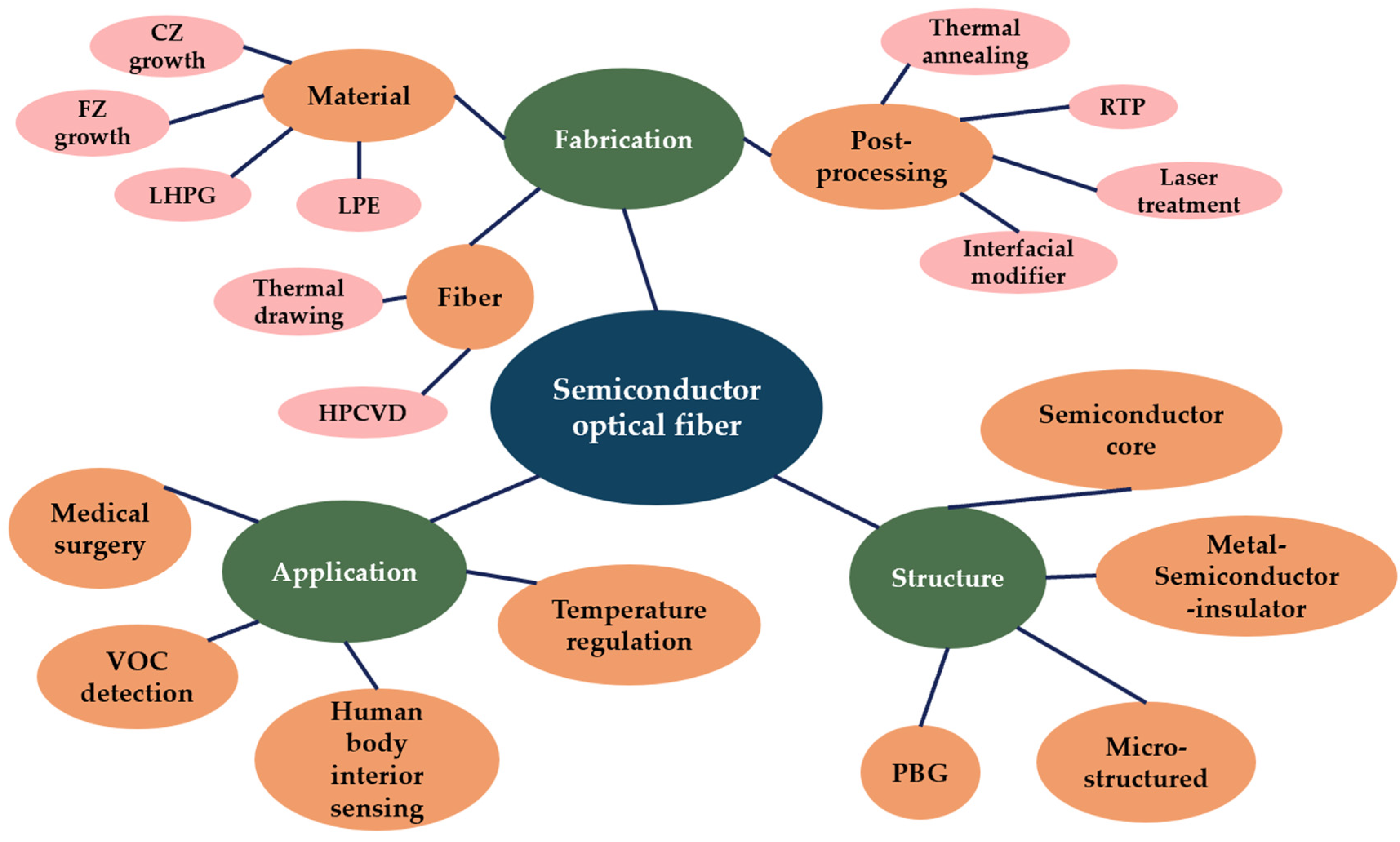
In this paper, we review semiconductor multifunctional optical fiber fabrication and biomedical applications. In Section 2, methods for producing semiconducting materials and semiconductor optical fibers and for enhancing fiber performance are introduced. In Section 3, we cover the most common semiconductor optical fibers of different structures, including semiconductor core fibers, metal-semiconductor-insulator fibers, MOFs, and PBGs. In Section 4, biomedical applications of semiconductor multimaterial fibers, including human body temperature regulation, in vivo lesion detection, volatile organic compound (VOC) detection, and neurosurgery lasers, are discussed. Figure 1 shows a summary of this review of biomedical semiconductor optical fibers.
2. Fabrication of Semiconductor Optical Fibers
Because of their thermal and mechanical mismatch with typical glass materials, the fabrication of optical fibers from semiconductors is a considerable challenge for the field of materials science [70]. As a result, the platform for optical fibers has been restricted to materials that are consistent with the typical fiber drawing techniques for an extended period. In 2006, a chemical deposition approach was used to create the initial example of a crystalline semiconductor optical fiber [25]. As a result of this endeavor, different methods have been utilized in the fabrication of semiconductor optical fibers. Each of these methods has its own set of benefits and drawbacks. However, since there have been no standardized techniques for fabricating these fibers, their production is relatively costly. This section provides a review of these various methods of fabrication and evaluates the relative benefits of each approach.
2.1. Material Fabrication
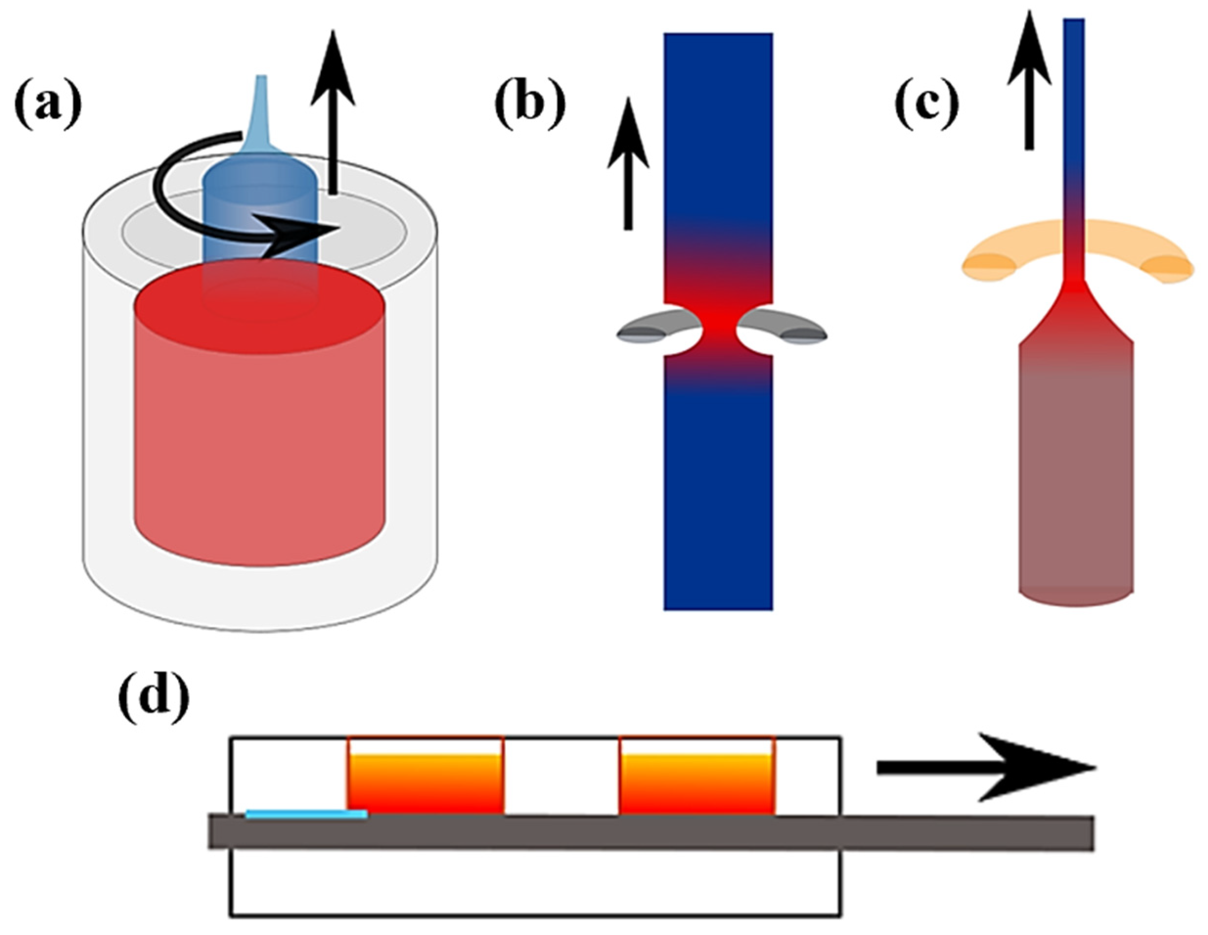
The production of fabrication begins with material fabrication. Commonly used methods for fabricating semiconductors, such as silicon, germanium, and selenium, include CZ growth, FZ growth, LHPG, and LPE.
CZ growth is the most popular approach to fabricating single-crystal silicon [71]. The process is depicted in Figure 2a. A single crystalline charge is heated over its melting point to form a melt, then a silicon crystal seed is inserted into the melt, and the crystal is progressively removed from the melt and rotated in the opposite direction to the melting crucible [72]. Key factors to control the fabrication process include the rotation rates of the seed and crucible and the pull rate of the seed [73]. In the early phase of CZ growth, the pull rate is large, and the fabricated crystal is small in diameter (3–4 mm), which is dubbed the “neck” of the crystal. CZ growth was first utilized by Dash for producing dislocation-free crystals, and its use has become prevalent in the industry [73].
FZ growth is an alternate and straightforward way of producing a bulk semiconductor crystal of homogeneous composition. If it is possible to create a feed rod with a uniform composition, then a steady-state condition might be created by selecting the growth parameters in such a way that the composition in the melt spontaneously controls the growth temperature [54]. For FZ growth, an inert gas or vacuum atmosphere is employed, and silicon’s surface tension enables a melt zone to be translated vertically down a high-purity rod [51], as depicted in Figure 2b. While reducing convection, magnetic forces stabilize the melt, and temperature gradients may reach tens of Kcm−1 [74,75]. During oxide crystal formation in optical furnaces [76], average bulk growth rates are mm per minute, and the greatest FZ temperature gradients are on the scale of 500–1500 Kcm−1 [76]. These characteristics are similar to fiber recrystallization. Carbon and oxygen residuals in FZ silicon boules are very small (on the order of 1016 cm−3), but in the case of fibers, the existence of oxide cladding may prevent impurities from being reduced to a small amount.
The production of oxide fibers has shown to be the most successful use of LHPG [55], as illustrated in Figure 2c. Temperature gradients for the LHPG technique can reach 104 Kcm−1, which is comparable to the values that have been reported for CO2 laser treatment of fibers [59,77,78], even though the unconstrained surface may result in undesirable diameter and surface quality variations. In the production of the quartz suspension fibers used as gravity wave detectors [79,80], a more sophisticated version of this optical technology is utilized. This technique is now commercially accessible for the tapering of optical fibers. Tapering stations have been effectively employed in the recrystallization of silicon core fibers [81,82], which has led to the production of crystalline cores with exceptionally high optical quality.
Since its development by Nelson in 1963, LPE has been used to build thin layers of III-V, II-VI, and IV-V1 alloys for material research and device applications [56], as demonstrated in Figure 2d. LPE structures have been utilized to make several electronics and OE. For example, GaAs/GaA1As double-heterostructure (DH) laser diode room-temperature CW lasing [83,84]. CW operation of DH lasers radiating beyond 1 μm was initially accomplished using LPE material in InP/InGaAsP [85], GaAsSb/GaA1AsSb [86], and GaSb/GaA1AsSb [87]. Studies of LPE literature are crucial in systems where the starting semiconductor charge is disproportioned, e.g., pulling InGaSb core fibers [88]. Sb filaments were detected in the as-drawn fibers, and this excess metal functioned as a recrystallization solvent [89]. Intentionally introducing an excess binary system material may produce a crystallization process similar to LPE in a closed vessel where oxidation issues are decreased. Crystal growth rates are often greater with fibers than with LPE, and few studies of a gradient perpendicular to the growth front for the latter method report maximum values of 25 K cm−1 [90,91]. Despite varied circumstances, LPE expertise may be applied to the fiber core and used to explore novel materials and solvent combinations for traveling zone expansion.
![Biosensors 12 00882 g002]()
Figure 2.
Material fabrication techniques. (Reprinted with permission from ref. [51]. Copyright 2021 Ursula J. Gibson et al.): (a) CZ growth, (b) FZ growth, (c) LHPG, and (d) LPE.
Figure 2.
Material fabrication techniques. (Reprinted with permission from ref. [51]. Copyright 2021 Ursula J. Gibson et al.): (a) CZ growth, (b) FZ growth, (c) LHPG, and (d) LPE.

2.2. Semiconductor Optical Fiber Fabrication Process
2.2.1. Thermal Drawing
Thermal drawing is one of the most commonly employed techniques to fabricate semiconductor optical fibers. The fabrication process should meet some of the following requirements. First, cladding materials should possess high viscosity to resist stretching stress. The viscosities and expansion coefficients of amorphous materials should be comparable to prevent deformation of the interface. Second, the temperature window during the fabrication process needs to be large enough to prevent amorphous materials from crystallizing. Last, chemical reactions during thermal drawing must be utilized to create novel materials during fabrication or to prevent fabrication. For example, the reaction between Al and silica can be utilized to create silicon core fibers [92].
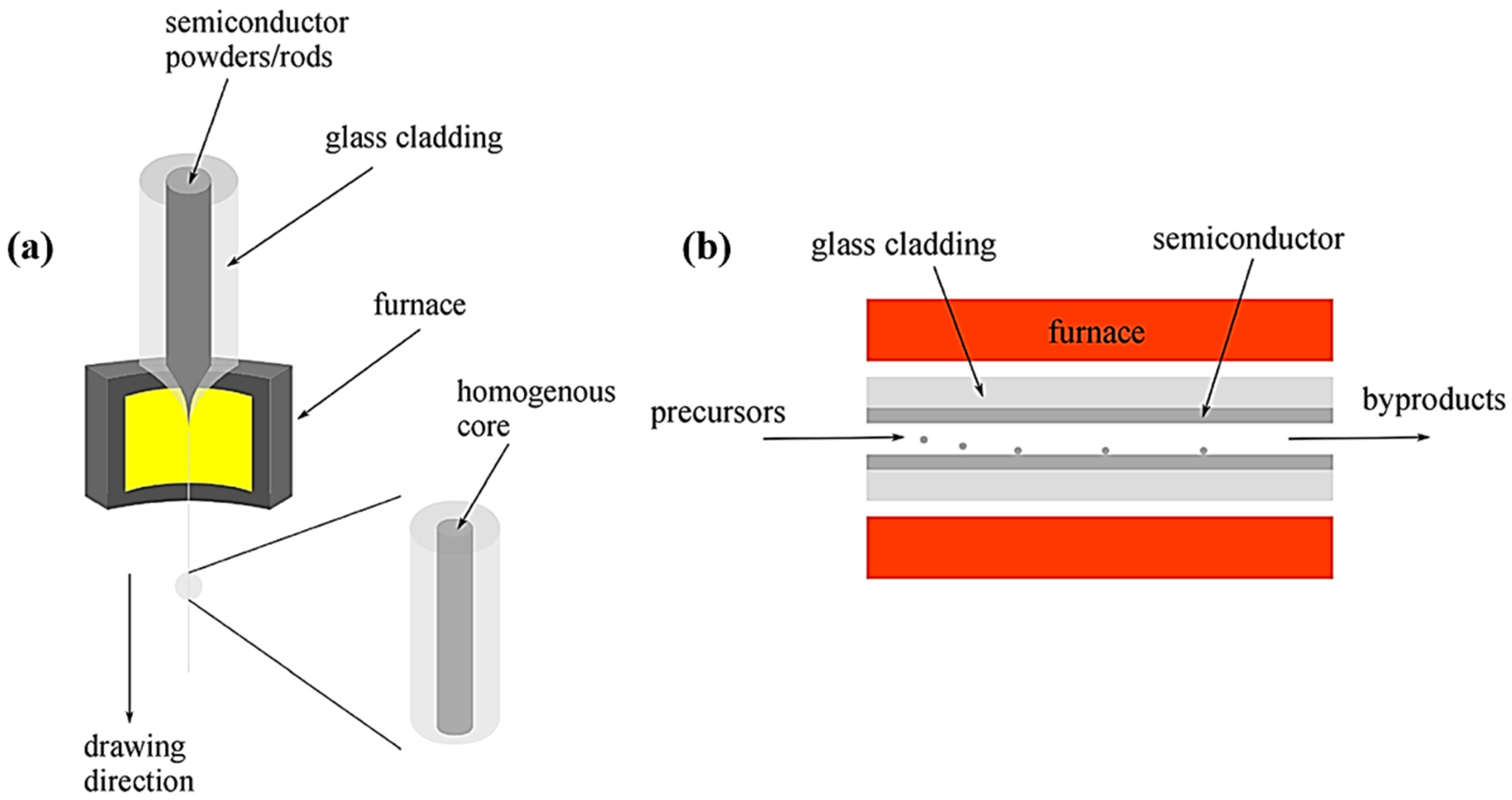
The process is summarized In Figure 3a. A preform is heated using a drawing tower furnace with a temperature that is 50–100 °C higher than the preform cladding glass transition temperature; the preform is drawn by a capstan while the materials within it are softened. Consequently, a fiber with diameter Df is fabricated. The consequent fiber has the same geometry as the preform. Df can be adjusted by the preform diameter Dp, preform feeding speed vf, and drawing speed vd [14]. This relationship is demonstrated as follows:
A unique technique using drawing towers for producing semiconductor core fibers is referred to as the MCM. The selection criteria for the MCM are similar to the criteria for thermal processing, while semiconductors are confined in cladding material and melt during heating. The MCM can be used to fabricate a variety of unconventional core materials with amorphous or crystalline features. Using the MCM to fabricate semiconductor optical fibers, core materials are placed in a tube that acts as the cladding material; then, through drawing towers, the tube is pulled in a thin robe. After drawing, the core gradually solidifies as the temperature drops; thus, a fiber is fabricated using the MCM. Because of the inconsistent cooling speed, the core might be amorphous or polycrystalline. The light propagation loss in the polycrystalline core optical fiber increases as the scattering loss increases [51]. As a result, postprocessing techniques are needed to enhance the fiber light conducting performance.
![Biosensors 12 00882 g003]()
Figure 3.
Fiber fabrication techniques. (Reprinted with permission from ref. [93]. Copyright 2021 Hei Chit Leo Tsui et al.): (a) thermal drawing and (b) HPCVD.
Figure 3.
Fiber fabrication techniques. (Reprinted with permission from ref. [93]. Copyright 2021 Hei Chit Leo Tsui et al.): (a) thermal drawing and (b) HPCVD.

2.2.2. High-Pressure Chemical Vapor Deposition
HPCVD is a hybrid method of engineering disciplines to integrate semiconductors and metals into MOFs. HPCVD is currently developed to deposit semiconductor nanowires, coaxial heterojunctions, and other patterned structures inside fibers [66]. High-pressure flow in MPa level can eliminate mass-transport constraints because the fibers’ high tensile strength overcomes the constraints of mass transport [94]. In addition, by considering pores in an MOF template as small chemical reactors, which can be injected into different chemical precursors, it is possible to deposit uniform, thick, and annular deposition on the heated pore walls across lengths ranging from centimeters to meters [95], as shown in Figure 3b.
As the functional materials inside fibers can be chemically deposited in independent stages, enabling fibers to possess design flexibility, fibers fabricated by the HPCVD technique can be further utilized to design fiber-integrated devices, including photoconducting detectors [96], fibers for infrared laser transmission [97,98,99], fibers for thermal sensation [100], radial fiber lasers, and wearable 2D and 3D array light detectors [101]. Although the length of fiber fabricated by HPCVD does not seem to be as scalable as that manufactured by drawing, semiconductor layers of 10 m in length have been accomplished, and larger lengths are conceivable [102]. In addition, HPCVD is extensible for deposition in several fibers using a single high-pressure precursor source, possibly enabling the concurrent fabrication of up to hundreds of fiber devices.
2.3. Postprocessing
As the core states are mostly polycrystalline or amorphous in fibers after thermal drawing, postprocessing is frequently necessary to increase the material quality or optimize the fiber shape to fully harness the fibers’ potential. Postprocessing techniques can enhance the performance of semiconductor optical fibers by increasing the crystallinity of semiconductors inside or by reducing element contamination, such as oxide contamination from glass cladding. All postprocessing procedures, with the exception of techniques aimed at reducing element contamination, rely on either thermal annealing or melt-recrystallization to heat a sample [93]. Common techniques used to enhance the multifunctional performance of fibers include thermal annealing [58], RPP [59], the interfacial modifier method [60], and laser treatment [61]. Figure 4 depicts the former postprocessing techniques.
2.3.1. Thermal Annealing
Thermal annealing is a process for controlling the characteristics of materials via crystal formation. During the process, materials do not remelt or recrystallize but rather have controlled nucleation of crystals, during which flaws are removed, and grain sizes are increased [93]. Thermal annealing can control the orientations of crystals that are produced, which may be crucial for certain purposes, such as nonlinear optics. Thermal annealing and rapid photothermal annealing are the two most common annealing techniques utilized for semiconductor optical fibers [103,104]. To effectively grow large crystal grains inside fibers, the technique involves two steps. First, fibers are heated to a low temperature of approximately 530 °C for 3 days to control nucleation site numbers, and second, the fibers are heated to approximately 1300 °C for 10 min. Compared with the pre-annealed fiber, the resulting fibers exhibited a much lower dislocation density and optical loss [105]. In this case, crystal sizes were restricted to 100 µm. Typically, thermal annealing is performed to transform amorphous semiconductor core material generated by the HPCVD technique into crystalline material. Moreover, both the absorption spectra and temperature performance can be changed by thermal annealing, as the technique can shift the bandgap of semiconductors and enhance the PL intensity [106]. It has been observed that SiGe alloy fibers produced by thermal drawing were subsequently annealed in a box furnace with a controlled heating rate [58]. Due to grain-to-grain diffusion, the homogeneity of the fiber core and optical performance of the fiber were enhanced.
2.3.2. Rapid Photothermal Processing
The rapid thermal processing (RTP) technique that is dominated by quantum effects is referred to as RPP. RPP allows semiconductor devices to be treated at temperatures that are lower than those required by RTP. As a result, RPP can produce semiconductor optical fibers with improved performance. The high throughput of RPP, in conjunction with its low processing temperature, offers new possibilities for devices such as solar cells, silicon integrated circuits, and flat panel displays [107]. Photons with wavelengths of less than approximately 400 nm are essential to witness quantum phenomena. Quantum effects have several positive consequences for RPP. First, the bulk and surface diffusion coefficients are increased. Second, less time is spent in each cycle of processing. Third, there is a significant decrease in the number of microscopic flaws, which results in improved performance [107,108]. In the case of RPP, the bulk and surface diffusion coefficients are greater than those of RTP and standard furnace processing. Additionally, quantum photo effects have a crucial role in ion implantation [109]. In regard to performance, reliability, and yields, RPP will deliver a significant improvement over other production processes. RPP makes available materials that have consistent microstructures and built-in dependability [108].
2.3.3. Laser Treatment
Laser treatment of semiconductors inside optical fibers is a very adaptable technique that can be utilized to change the semiconductor material in a variety of ways. For instance, CO2 laser processing has been utilized to heat fibers and recrystallize fiber cores, thereby resolving the uneven segregation issue of semiconductor alloys during nonequilibrium solidification and improving optical transmission behavior [59] by accurately regulating the heating temperature and cooling speed to produce single-crystal semiconductor materials [77]. This technique allows the fabrication of semiconductor core fibers of any length with low loss. Similar techniques have been employed to reduce the optical loss of germanium core fibers [110]. In contrast to conventional annealing techniques, the semiconductors of fiber are regionally heated to a molten state and then recrystallized under precise control as the fiber is scanned past the laser’s focal point [93]. Unlike tapering methods, which must equally heat the core and cladding materials, laser processing allows for selective heating of either the core or the cladding, depending on the selected wavelength.
Two primary heating methods have emerged concerning laser treatment. The direct optical absorption of the laser beam was the first method shown to successfully heat and melt the core. A laser source with photon energy larger than the semiconductor’s electronic bandgap is utilized since this kind of laser can pass through the cladding material but is significantly absorbed by the core through electronic absorption. By adjusting the scan rate, we may manipulate the strain and the electronic bandgap of the material. The second method involves the use of heat carried from the cladding to melt the semiconductor. For silica cladding fibers, CO2 lasers are commonly employed as the source since they can be absorbed by the cladding material. This technique allows for the development of single crystals with cm-scale lengths and high aspect ratios with minimal strain [77,111]. Both methods may be used in combination, with energy being absorbed by the core and cladding in a single manufacturing step.
2.3.4. Interfacial Modifier
The utilization of an intermediate layer between the semiconductor core and the silica cladding can reduce tension, expel pollutants, and establish a gradient index of refraction [112]. A suitable interfacial material should meet the following guidelines. First, the material should be an oxide to reduce chemical sophistication; second, the material should form a eutectic with a semiconductor inside the fiber and possess a softening point that is higher than the semiconductor material to alleviate tension; last, the metal ion of the oxide should be less electronegative than the semiconductor to aid oxygen scavenging from the core [60]. Calcium oxide meets the aforementioned characteristics and is often employed in the purification of silicon [113], similar to other alkaline earth oxides. CaO reacts with water to create hydroxides; hence, a preform with a CaO layer on the interior of the silica may be prepared using an aqueous process. Further studies of NaO, BaO, SrO, and MgO were conducted with varying degrees of success: SrO and NaO, as well as NaO-BaO mixes, were the least successful, leading to deformation of the glass–silicon interface or immense voids in the core, while CaO and CaO-MgO blends behaved the best. Prior research mostly focused on the mechanical and microstructural qualities of the material. The optical characteristics of the fibers may be enhanced by using more pure raw materials [60].
3. Main Structures for Semiconductor Optical Fibers
We have thus far described several fabrication techniques and postprocessing methods for semiconductor multimaterial optical fibers. In this section, we will discuss the most common structures for semiconductor optical fibers, including semiconductor core fibers, metal-semiconductor-insulator fibers, MOFs, and PBGs. The geometries of the semiconductor optical fibers are shown in Figure 5.
3.1. Semiconductor Core Fiber
Semiconductor core fibers may combine nonlinear, Raman, and IR transparency of semiconductor planar waveguides with the advantages of long, elastic, and resilient fiber-based waveguides [114]. The most frequently employed technique for fabricating optical fibers that contain semiconductor cores is the MCM, as mentioned in the former section. For the MCM to work, the cladding glass has to soften and draw at temperatures higher than the core’s melting point. Initial measures employed silica glass as a cladding material for silicon core fiber, whereas DURAN, an alkaline borosilicate glass, was utilized for germanium core fiber. Silicon melts at approximately 1414 °C, while silica crystallizes at approximately 1950 °C. Although it would be preferable if the draw temperature more closely matched the melting point of the core, silica is commercially accessible and has high strength. For germanium and DURAN, a superior thermal match is achieved, as germanium melts at approximately 938 °C, whereas DURAN melts at approximately 1000 °C. After fiber fabrication, oxygen from cladding glass is detected in the fiber core, and its concentration increases with decreasing core size [114]. The oxygen concentration of the germanium core is much lower than that of the silicon core. The main reasons for the concentration difference can be described as follows. First, the higher temperature of silicon core (1950 °C) fiber thermal drawing activates more oxygen dissolution than germanium (1000 °C) [115]. Second, at high temperatures, germanium oxide is volatile [116,117]. In this instance, germanium oxidation melt produces a volatile product that, given the low viscosity of the germanium melt [118], should diffuse from the molten core.
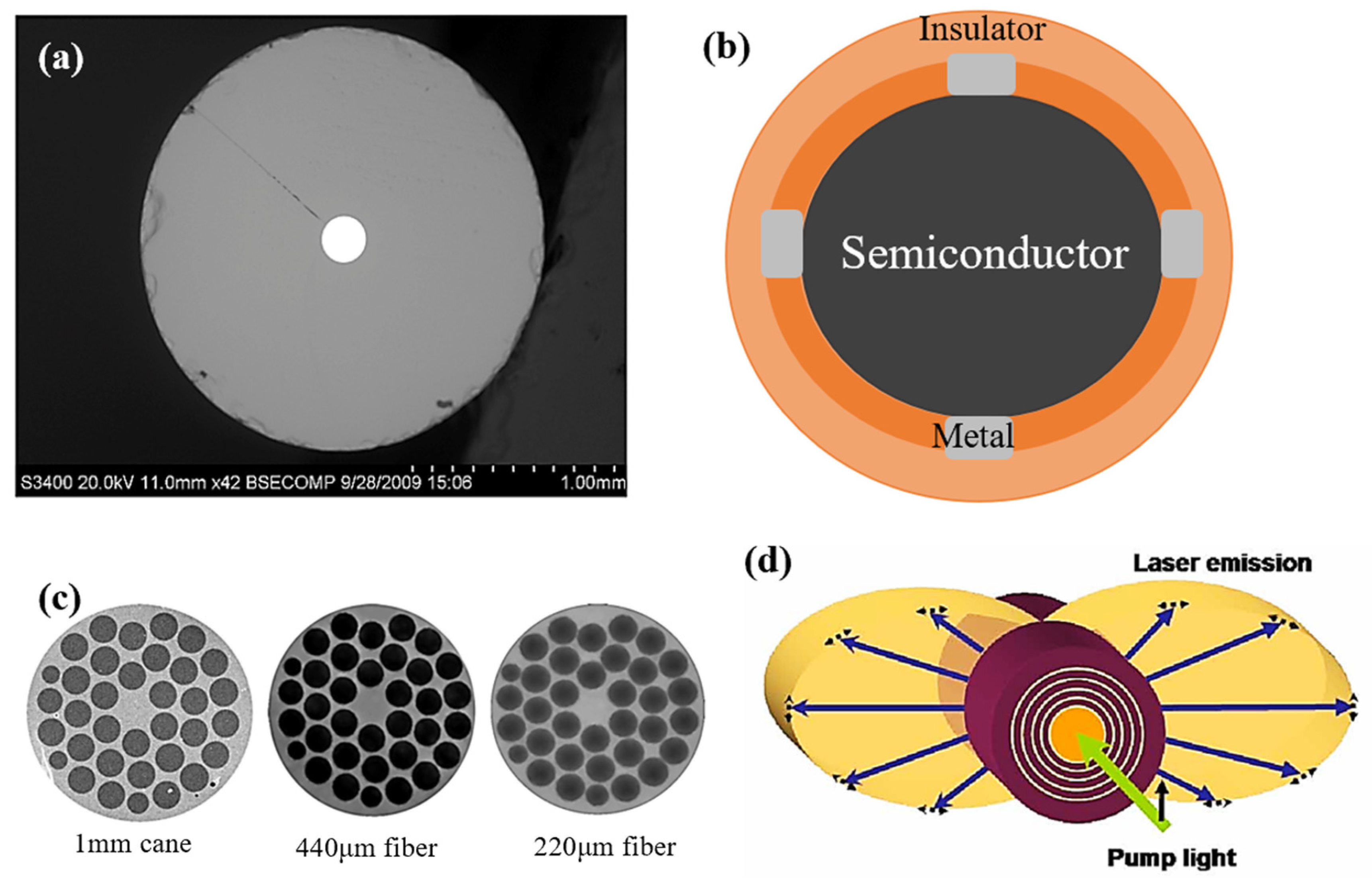
![Biosensors 12 00882 g005]()
Figure 5.
Semiconductor optical fibers of different geometries: (a) semiconductor core fiber (Reprinted with permission from ref. [119]. Copyright 2010 Optical Society of America), (b) metal-semiconductor-insulator fiber, (c) MOFs (Reprinted with permission from ref. [120]. Copyright 2003 Optical Society of America), and (d) PBG fiber (Reprinted with permission from ref. [121]. Copyright 2006 Optical Society of America).

3.2. Metal-Semiconductor-Insulator Fiber
Most practical electrical and OE devices require a combination of conductors, semiconductors, and insulators with well-defined geometries and at stipulated length scales while generating intimate surfaces [24]. Typically, the fibers are manufactured utilizing a variety of complicated wafer-based methods, which permit microscopic features but are constrained to planar geometries and restricted covering areas [122]. In comparison, the procedure of pulling fibers from a prefabricated reel or tube is easier and produces longer, highly uniform fibers with controlled geometries and excellent optical transport characteristics. This method has thus far been limited to certain materials [123] and larger features [124]. Thermal drawing can be utilized to fabricate a fiber photodetector with a core of amorphous semiconductors surrounded by metallic microwires. Such a fiber is sensitive to light over its whole length (tens of meters), constituting a one-dimensional photodetection element. The fiber can be woven to design a grid of fibers that are capable of identifying the position of an illumination point.
The variety of metal-semiconductor-insulator fiber structures enables fibers to possess various functions. A fiber that integrates optical, electrical, and thermal components can act as a self-monitoring optical transport device [125]. To direct high-power radiation along the fiber axis [126], hollow-core multilayer cylindrical PBGs [127,128] are utilized in the fiber transmission element. To keep track of the temperature throughout the length of the fiber, long metal wires connected at their ends by a semiconductor layer respond to changes in the fiber’s temperature by sending a current to the fiber’s terminals. Self-monitoring, high-power optical transmission lines can predict and prevent failures because the electrical conductivity of the semiconducting material exponentially depends on temperature, allowing for instantaneous discrimination between normal transmission conditions and those indicative of localized defect formation [125].
3.3. Microstructured Optical Fiber
MOF is an innovation that is characterized by a series of nanoscale capillaries to microscale capillaries. These capillaries are designed in geometries to guide light via photonic bandgap effects [129,130]. Physical methods such as drawing and fluid infiltration are being used to include gases [131], liquid crystals [132], polymers [24], and low-melting-point solids, including metals [133,134], compound glasses [25], and semiconductors in MOFs, hence increasing the versatility and utility of fiber devices [123,135]. High-performance semiconductors and junctions are indispensable for use in high-performance OE and photonics [136]. Transistors, light-emitting diodes/lasers, and high-speed photodetectors rely on p-n junction creation, which is enabled by carefully managed impurity doping.
MOFs can be deposited by the HPCVD technique, which can integrate conformal semiconductor layers and void-free wires inside micro-to-nanoscale-diameter pores [95]. The use of fibers as templates for the manufacturing of these semiconductor devices enables more geometric design freedom than is possible with planar fabrication. Thus, all-fiber technical approaches are realized by enabling the seamless integration of OE and photonic devices with fiber infrastructure. Junction-based fiber devices with gigahertz bandwidth, for instance, can be manufactured from doped crystalline semiconductors [95]. As it is impossible to draw on amorphous hydrogenated silicon, its nonlinear optical properties may be exploited by fiber deposition. Ultimately, the cores of fibers fabricated from crystalline compound semiconductors show promise for high-power infrared, light-guiding fiber devices and subwavelength-resolution, wide-area infrared imaging.
In the procedure, pressures ranging from 8 to 35 megapascals are applied to MOF pores to force chemical precursor mixtures, such as silane and dopants in a gas mixture of helium or carbon dioxide, to flow through the MOF holes. At temperatures that have been properly selected, the precursor breakdown, layer deposition, and dopant integration processes take place within the pores. Amorphous semiconductors, such as Ge, may be deposited at lower temperatures using group IV hydride precursors. Polycrystalline semiconductors, such as crystalline Si tubes, can be formed by annealing amorphous materials at elevated temperatures [123].
3.4. Photonic Bandgap Structured Fiber
PBGs, commonly referred to as photonic crystals (PCs), emerged from an original concept by Eli Yablonovitch [137]. For PBG materials, the propagation of photons in a certain energy range is likewise prohibited. On a length scale comparable to optical wavelengths, PBGs exhibit an alternative refractive index [137]. PBGs may be classed as 1D, 2D, or 3D. 1D PBGs are generally composed of alternating dielectric layers with alternative refractive indices. 2D PBGs may be planar structures having a periodic pattern in two dimensions or PBG fibers [138], for example, the hollow core, or depressed index solid core PBG fibers, where a PBG is in the cladding. 3D PBGs have a periodic refractive index in three dimensions and often include the opal or inverse opal type.
An omnidirectional dielectric mirror fiber was fabricated by thermal drawing from a multilayered fiber preform [20]. Glassy materials with very different refractive indices but equivalent thermomechanical capabilities were employed to create 21 layers of alternating refractive indices that surrounded a durable polymer core. These fibers might be used in a variety of contexts, such as woven radiation barriers, spectral identification of cloth, and telecommunications filters. Dielectric mirror fibers that act as omnidirectional mirrors may redirect light from any direction and of any polarization that strikes them. Altering the layer thickness by just a few atomic layers may produce transmission spectra that span the electromagnetic spectrum. The transmission peaks in the visible, ultraviolent (UV), near-infrared (NIR), and middle infrared (MIR) sections of the optical spectrum for fibers with various layer thicknesses. Due to the modest material absorption, multimaterial hollow-core, PBG optical fibers may provide lasers with low transmission loss at peak outputs of 11.4 MW at 1.55 μm, with 97% of the fiber output in the fundamental mode [139].
4. Potential Biomedical Application
4.1. Thermoelectric Fiber for Human Body Temperature Regulation
Based on the Peltier effect and Seebeck effect, the applications of TE devices may be categorized into two groups: fiber-based thermoelectric coolers (FTECs), which transfer electrical energy into heat, and fiber-based thermoelectric generators (FTEGs), which transfer heat into electrical energy [140]. Popular inorganic TE materials are shown in Table 1. FTECs have features such as small volume and precise temperature control without vibration and noise. Despite their hard construction, these devices have been employed to replace more conventional methods of cooling, such as those used in refrigerators and electronic gadgets’ central processing units [141,142,143]. As a bonus, solar energy may be used by coolers in tandem with a heating system to both chill and warm an area throughout the summer and winter months [144]. The application of FTECs may decrease environmental pollution and climate change [145]. FTECs can accomplish this reduction because they are more adaptable and lightweight than conventional TECs, hence mitigating their disadvantages [146]. When the ambient temperature is greater than the normal skin temperature, a fabric system containing FTECs may maintain a cool microclimate. Consequently, such clothing is particularly effective for preventing heat stroke for persons who operate in high-temperature environments, such as construction workers in subtropical and tropical countries and steelworkers [140]. In addition, FTEGs have a vast promising application scope, ranging from space and military to autos, aircraft, biomedicine, and smart textiles, and can employ a variety of heat sources, such as biothermal and waste heat from transportation equipment. When astronauts conduct extravehicular activities in outer space, where the temperature ranges from −233~121 °C, they wear hermetic space suits [147]. Liquid cooling and ventilation are conventional space-suit thermal management methods. The ventilation unit or airflow duct on this clothing reduces its air permeability [148]. FTECs and FTEGs combine their benefits to solve the temperature and moisture comfort challenges of current space suits. When outer space is hotter than the body temperature, FTEGs will power FTECs [149]. This application can be further introduced to patient body temperature; common medical applications for semiconductor FTEGs are depicted in Figure 6.
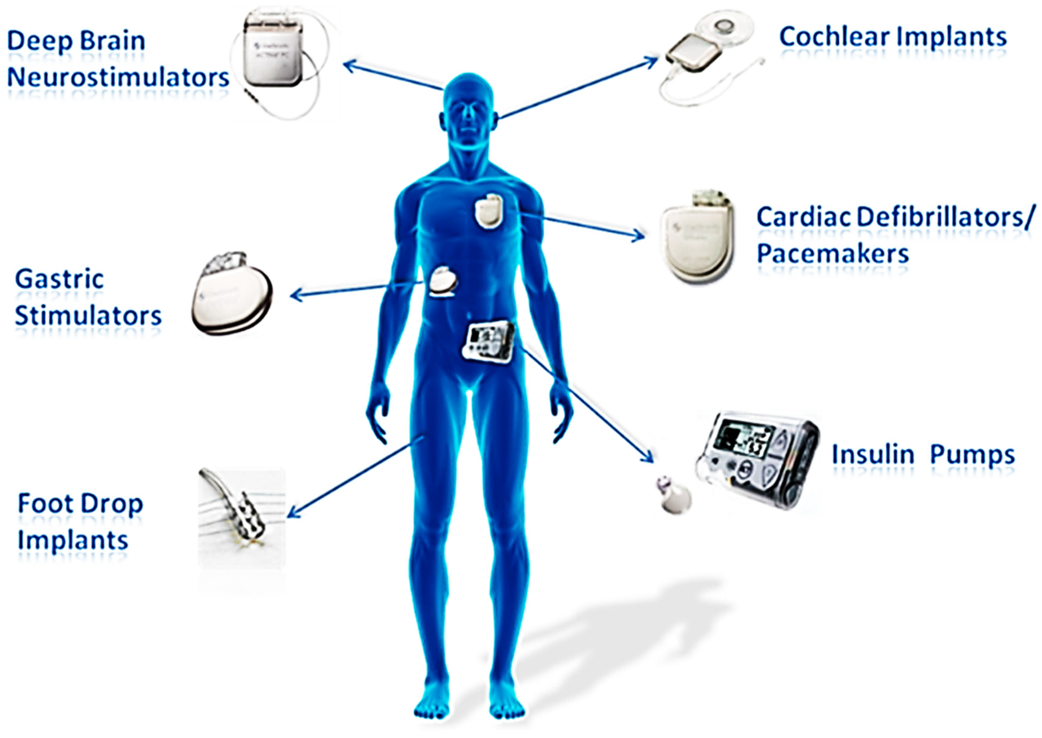
In addition, the transformation of human body heat into electric power is one of the most significant uses of textile-based FTEGs. Human body heat is generally maintained at 37 °C and created via metabolic processes [150]. The most apparent benefit of the transformation is that energy can be collected regardless of activity and may be gathered from the whole body’s surface. Textile-based FTEGs may thus be utilized to support the functioning of small electronic devices, such as sensors and implantable medical devices (IMDs), such as cochlear implants, drug pumps, neurostimulators, muscle stimulators, and pacemakers. These gadgets only need a few microwatts to milliwatts of power to operate [151,152,153]. Since the introduction of the first implantable medical device in 1972, IMDs have been extensively utilized for diagnosis, prognosis, and therapy [154]. One difficulty in the development of IMDs is that their batteries, the device’s energy source, may reach the end of their useful life after prolonged use [155]. A reliable and continuous power source is essential to sustain the functionality of IMDs to prevent needless surgery and patient costs. Consequently, the use of FTEGs to power IMDs is a viable solution to this issue.
![Biosensors 12 00882 g006]()

Table 1.
Popular inorganic TE materials.
| Inorganic TE Materials | Type | ZT | Temperature(K) | Reference | |
|---|---|---|---|---|---|
| Half-Heusler compound | Hf0.6Zr0.4NiSn0.98Sb0.02 | n-type | ≈1.0 | 1000 | [156] |
| Zr0.5Hf0.5CoSb0.8Sn0.2 | p-type | 0.8 | 973 | [157] | |
| Hf0.8Ti0.2CoSn0.8Sn0.2 | p-type | 1.0 | 1073 | [130,158] | |
| Bi-Te alloy | FeNb0.86Hf0.14Sb | p-type | ≈1.5 | 1200 | [159] |
| BixSb2-xTe3 | p-type | 1.4 | 373 | [160] | |
| Bi0.3Sb1.7Te3 | p-type | 1.33 | 373 | [161] | |
| Bi0.5Sb1.5Te3 | p-type | 1.25 | 320 | [162] | |
| Bi2Te2.79Se0.21 | n-type | 1.2 | 357 | [163] | |
| Skutterudite compounds | Co3.2Fe0.8Sb12 | p-type | 0.53 | 823 | [164] |
| Ca0.31Co4Sb12 | p-type | 1.15 | 840 | [165] | |
| CeFe4Sb11.9Te0.1 | p-type | 0.76 | 773 | [166] | |
| La0.75Pr0.25Fe4Sb12 | p-type | 0.83 | 823 | [167] |
Figure 6.
Common semiconductor implantable devices. (Reprinted with permission from ref. [168]. Copyright 2019 PM Kumar et al.).
Figure 6.
Common semiconductor implantable devices. (Reprinted with permission from ref. [168]. Copyright 2019 PM Kumar et al.).

4.2. Optoelectronic Fibers for Sensing the Human Body’s Interior
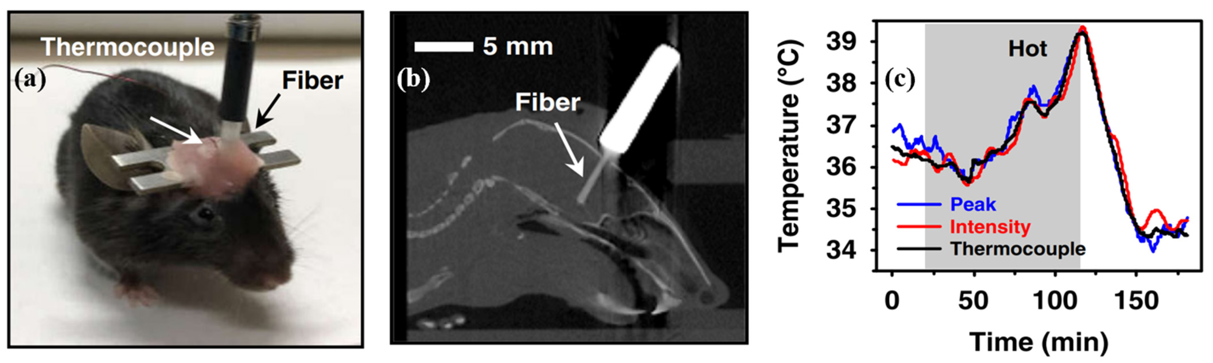
One typical use for optical fibers is in the field of optical detection. OE qualities are necessary for multimaterial fiber photodetectors that are used in medical applications, such as internal observation and imaging. Various semiconductors possess a wide range of characteristics, making semiconductor OE fibers appealing [169]. These characteristics include a broad range of infrared transparency, significant optical nonlinearity, and a high refractive index [66]. All examples of nonlinear behavior in semiconductor optical fibers have been linked with centrosymmetric crystal systems, with the major portion associated with the silicon fiber framework [93]. The transformation of optical power into electrical power is the fundamental process that underpins the majority of semiconductor-detecting or energy-collecting OE devices [170]. This transformation is a significant advantage of the semiconductor OE fiber platform over other similar technologies. Both in-fiber detectors and “solar threads” have been manufactured using this technology to achieve this goal [102,123]. This platform is distinguished from previous fiber technologies by the possibility of incorporating OE functionality into the constituent material of the waveguiding fiber. Moreover, the OE property can be further utilized to detect in vivo temperature, as demonstrated in Figure 7. The fiber-integrated device can measure deep brain temperature variations. Complementary to tethered electrical sensors, this optical-based approach is more appropriate for use in areas with significant electromagnetic interference and is especially capable of acquiring data during magnetic resonance imaging (MRI). As a result, various fiber optic sensors based on OE characteristics, such as the bandgap of a GaAs crystal material [171], have been implemented [172,173].
The most common geometry for multimaterial OE fibers is a metal-semiconductor-insulator fiber, as mentioned in the former section. Within a cladding constructed of transparent thermoplastic, the earliest kinds of OE fibers combined metals, polymer composites, and chalcogenide semiconductors [66]. Chalcogenide glasses may be produced either by starting with the chalcogen elements S, Se, and Te or by adding additional elements such as As, Ge, Sn, or Ga [174]. The chalcogenide semiconductors integrated in OE fiber structures include As40Se50Te10Sn5 [24], Se97S3 [175], SnZn [131], and ZnSe [176]. The OE fibers are fabricated mainly through thermal drawing and HPCVD.
The first metal-semiconductor-insulator OE fiber was produced by thermal drawing [24]. The photoconducting fiber could be employed to detect incoming light on the fiber’s surface along its length. After weaving these fibers into grids, it is possible to determine the phase and amplitude of an electromagnetic wave across wide regions for lensless-free imaging systems [177]. Within the confines of a single fiber, it was possible to create cascading thin films that combined several photodetection devices with feature sizes as small as 100 nanometers. The fiber was able to distinguish between two wavelengths in the visual range with a precision of less than 5 nm and an angular resolution that was accurate to within 4 degrees [178]. In addition, the assembly of these fibers into two-dimensional grids produced textiles that were able to both localize a point of light and carry out sophisticated optical tasks, such as the imaging of an object without the need for lenses [177,178]. The fiber’s infrared OE capability and adaptability enable it to function as an in vivo sensor to identify anomalies in human tissues and organs.
Utilizing HPCVD is another option for the monolithic incorporation of metals and semiconductors in fibers. Multiple devices, including ohmic contacts [66], p–n junctions [179], Schottky junctions [123], and p–i–n junctions [102], may be manufactured due to the sequential deposition of various materials. The Pt/n-Si Schottky junction that was manufactured using the HPCVD junction had a barrier height of 0.8 eV and displayed a 3 dB bandwidth with a maximum of 3 GHz at a wavelength of 1550 nm. These dimensions allowed photodetection to be performed at telecommunication wavelengths within a limited amount of time [123]. A polycrystalline silicon p–i–n junction is successfully achieved across a length of one meter of silica MOF. When lit across a length of 1 mm and subjected to 100 MHz waveguide photodetection at 1064 nm, the fiber had a bandwidth that reached 1.8 GHz, which was 3 dB wide [102]. Due to its increased quantum efficiency, this fiber is advantageous for its use in applications relating to photodetection and photovoltaics. Under the conditions of air mass 1.5 solar illumination, the total conversion efficiency of a 1 cm p–i–n fiber that was electrically connected on both ends showed a value of 0.5%. This fiber is effective for photodetection due to its high quantum efficiency and may be incorporated into medical equipment for lesion exploration during gastrointestinal and colonoscopy surveillance.
![Biosensors 12 00882 g007]()
Figure 7.
OE fiber-integrated devices for in vivo temperature sensing (Reprinted with permission from ref. [180]. Copyright 2022 He Ding et al.): (a) a mouse implanted with a fiber sensor for temperature detection; (b) sagittal CT slice reconstruction; and (c) dynamic temperature data acquired by the fiber sensor in the mouse brain.

4.3. Gas Sensor for VOC Detection
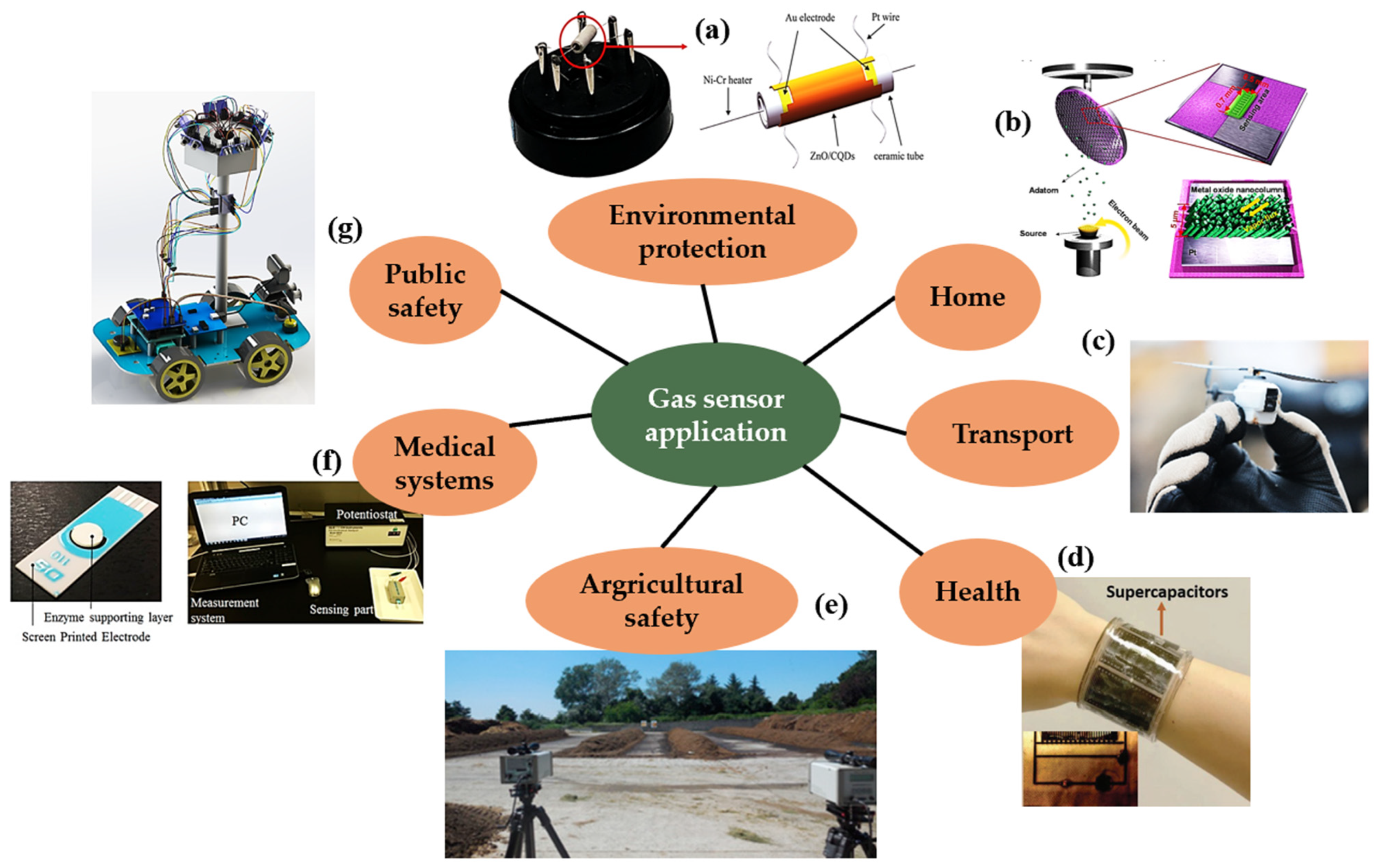
Disease-related gas detection is receiving growing medical interest. In healthy individuals, the amounts of VOCs in exhaled breath are often detected at subppm values or even lower values. Even if the association between a particular illness and certain VOCs has been recognized for more than a century, only current technologies based on semiconductor gas sensors can provide the quantitative measurements required for stringent clinical practice. Clinical experiments have shown the potential for utilizing breath to diagnose major diseases, including many forms of cancer, diabetes, multiple sclerosis, and kidney disease [181]. The invention and widespread use of solid-state gas sensors have offered an additional boost to the interest in VOC inspection and analysis for medical applications [182]. Semiconducting gas sensors are employed to test certain gases, such as hydrogen peroxide [183], acetone [184], ammonia [185], nitric oxide [186], and volatile sulfur [187], from human bodies. However, the study is being undertaken to create detection systems based on commercial MOX detectors to monitor low quantities of VOCs in breath [188], which is further enhanced by temperature modulation [189]. Particular breath biomarkers not only identify the existence of particular illnesses but also represent the overall physical state. An example of such gadgets is mobile acetone analyzers that monitor the ketone level and determine body fat burning rate only from exhaled breath. The devices that track fat metabolism and ketosis levels are widely utilized in a variety of diet and exercise regimens. SnO2 nanofibers functionalized with reduced graphene (rGO) that were assessed for the identification of acetone and hydrogen sulfide in human breath are an example of the utilization of semiconductors in breath analysis [190].
With health care applications, gas sensors are utilized for wearable biosensors. Wearable biosensors are small, complicated devices that have wireless connection modules for sending sensor data to computational infrastructure [191]. In such sensing devices, many chemicals are utilized. In the case of semiconducting oxide materials, this use presents a problem since the working conditions of the sensor must be lowered to room temperature. Nanostructures, such as graphene or nanowires, are one technique to attain this goal [192]. Recently, a stretchy and flexible, self-heating metal oxide (MOx) gas-sensing platform was developed [193]. Compared with their industrial equivalents, the development of wearable gas sensors must meet stringent criteria, such as a compact and lightweight form factor, low working temperature, low energy consumption, and mechanical durability upon diverse skin deformations. Latest applications of gas sensors are depicted in Figure 8.
4.4. Fiber Lasers for Medical Surgery
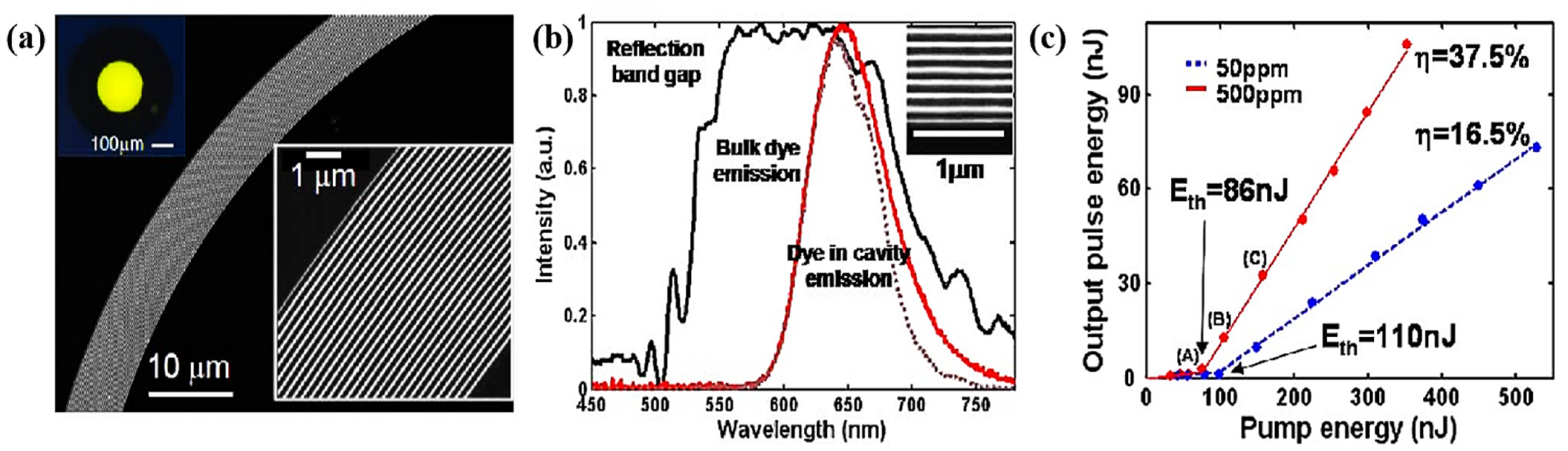
All fiber lasers that have been manufactured have been designed to emit light down the axis of the fiber, with the spot size determined by the core radius and the wavefront being virtually planar [195]. The cavity that is necessary for lasing is created by reflection off of the end facets of the fiber. There are numerous applications in which it is advantageous to deliver laser light in the radial direction over an extensive area [196]. Some examples of these applications include textile fabric displays [197] and biomedical applications ranging from photodynamic therapy [198] to in vivo molecular imaging [199]. A radial lasing structure [121] is produced as a consequence of omnidirectional reflection originating from an annular multilayer mirror that is lined inside of a hollow-core fiber. As shown in Figure 9, the fiber allows for the transmission of a pulse optical pump at 532 nm and covers the complete fluorescence spectrum (Figure 9b). Moreover, the dependency of energy on pump energy is shown for both 500 ppm and 50 ppm dye concentrations (Figure 9c). The slope efficiencies for the 500 ppm and 50 ppm concentrations are 37.5% and 16.5%, respectively.
Omnidirectional dielectric mirror fibers can reflect light incidence in any direction, independent of the angle or polarization. A minute modification to the layer thickness on the nanoscale scale may produce the spanning transmission spectra that are desired. The transmission of light through fibers that have varied layer thicknesses peaks in the visible, ultraviolet, near-infrared, and mid-infrared parts of the optical spectrum. Due to the low material absorption, multimaterial, hollow-core, PBG optical fibers are capable of delivering lasers with minimal transmission loss, with 97% of the fiber output occurring in the fundamental mode [139]. The transmission of high-peak-power laser pulses in highly controlled spatial patterns through fiber optics provides the foundation for a wide variety of medicinal and industrial applications [139]. Fibers with fundamental PBGs at 350 nm (UV) and 750 nm (NIR) have been utilized for biomedical purposes, whereas fibers with fundamental PBGs at 10.6 μm (MIR) have been used for laser surgery [195]. Because of the MIR wavelength laser’s strong water absorption at 2.9 μm in human tissue and small surgically damaged area [200], it is suitable for use in a wide variety of medical and surgical applications, including otorhinolaryngology, gynecology, neurosurgery, urology, dermatology, ophthalmology, dental surgery, and cardiovascular surgery [201,202]. The use of the CO2 laser in neurosurgery is superior. Because of its high water absorption rate, the CO2 laser generates minimal heat and protects the surrounding tissue [203,204]. There have been commercial fiber lasers for medical surgery. Semiconductor saturable absorber mirrors (SESAMs) with a quantum well structure placed on Bragg mirrors are the most developed and commonly used SAs in available commercial ultrafast lasers [205]. However, the intricate fabrication procedure of SESAMs utilizing molecular beam epitaxy renders them rather costly and rigid.
![Biosensors 12 00882 g009]()
Figure 9.
PBG fiber laser (Reprinted with permission from ref. [121]. Copyright 2006 Optical Society of America): (a) Fiber structure; (b) Fluorescence spectrum shown in red, and measured reflection band gap shown in black; (c) Dependence of the laser energy on the pump energy.
Figure 9.
PBG fiber laser (Reprinted with permission from ref. [121]. Copyright 2006 Optical Society of America): (a) Fiber structure; (b) Fluorescence spectrum shown in red, and measured reflection band gap shown in black; (c) Dependence of the laser energy on the pump energy.

5. Conclusions and Outlook
In this paper, a review of semiconductor multimaterial fibers was presented with respect to materials, fabrication methods, device structures, and applications. First, we take into account the manufacturing processes that are most commonly utilized to produce semiconductors and various methods that may be used to fabricate semiconductor multimaterial fibers, followed by post-fabrication procedures that improve the functionality of semiconductor optical fibers. Second, we discuss semiconductor optical fibers with different structures. Last, we describe the innovative functions that can be achieved by integrating semiconductors into fibers and their potential applications in medical and surgical procedures.
The developments of novel fiber materials and compositional structuring are key themes that arise from current works in studies on semiconductor optical fibers. The examination of the kinetics during fiber manufacture and postprocessing techniques generates positive effects on significant improvements in performance. Many different topics warrant additional research, the most important of which is the role of cladding-induced stress in determining whether clean grain boundaries are detrimental to optical applications. In addition, an exploration to limit the integration of impurities in fabricated fiber or remove impurities from fabricated fiber is important [51,119,206,207].
Although multifunctional fibers have had to rely on inorganic chalcogenide glasses for their OE functionality and simplicity of fabrication, it is anticipated that by provoking phase transitions [208,209,210], semiconductor crystalline domains with outstanding electronic properties can be incorporated within fiber devices. The use of OE and logic processes may be facilitated by the use of electronic junction structures, such as p-n junctions and Schottky junctions. Numerous additional qualities contribute to the usefulness of semiconductors. For example, the Kerr nonlinearity of As2Se3 is approximately three orders of magnitude larger than that of silica glass [211,212,213,214,215]. Therefore, the appearance of nonlinear optical phenomena predicated on these multimaterial glass fibers should be anticipated. Some examples of these effects include supercontinuum generation [216,217] and Raman amplification [218]. Other qualities include high magneto-optic coefficients [219]; these properties easily propose a vast variety of small fiber-based devices. Exciting new gadgets are on the horizon as more progress in the incorporation of electrical functionality into these fibers is achieved.
Fabrics woven entirely or in part from integrated fibers have the potential to deliver a wide variety of real-time, novel functionalities across the entire surface area of clothing. These functionalities are energized by electrical energy collected from the surrounding environment. The interaction between the characteristics of the materials and the integration of the structure in these fibers, coupled with the production of the fabric array, is emergent and has the potential to be an attractive subject for biomedical applications. Further advancement of transistors and fiber-integrated devices has the potential to produce increasingly more complex features and genuinely multifunctional textiles [195].
Author Contributions
Writing—original draft preparation, L.S.; writing—review and editing, C.T., H.B., Z.W., S.K. and R.M.; supervision, project administration, funding acquisition—C.T. and R.M. All authors have read and agreed to the published version of the manuscript.
Funding
This research was funded by the National Natural Science Foundation of China (62003046, 6211101138); Guangdong Basic and Applied Basic Research Foundation (2021A1515011997); Special project in the key field of Guangdong Provincial Department of Education (2021ZDZX1050); The Innovation Team Project of Guangdong Provincial Department of Education (2021KCXTD014); S. Kumar acknowledges Double-Hundred Talent Plan of Shandong Province.
Conflicts of Interest
The authors declare no conflict of interest.
References
- Al-Naji, A.; Gibson, K.; Lee, S.-H.; Chahl, J. Monitoring of Cardiorespiratory Signal: Principles of Remote Measurements and Review of Methods. IEEE Access 2017, 5, 15776–15790. [Google Scholar] [CrossRef]
- Min, R.; Hu, X.; Pereira, L.; Simone Soares, M.; Silva, L.C.B.; Wang, G.; Martins, L.; Qu, H.; Antunes, P.; Marques, C.; et al. Polymer Optical Fiber for Monitoring Human Physiological and Body Function: A Comprehensive Review on Mechanisms, Materials, and Applications. Opt. Laser Technol. 2022, 147, 107626. [Google Scholar] [CrossRef]
- Lin, S.-T.; Chen, W.-H.; Lin, Y.-H. A Pulse Rate Detection Method for Mouse Application Based on Multi-PPG Sensors. Sensors 2017, 17, 1628. [Google Scholar] [CrossRef] [Green Version]
- Alzahrani, A.; Hu, S.; Azorin-Peris, V.; Barrett, L.; Esliger, D.; Hayes, M.; Akbare, S.; Achart, J.; Kuoch, S. A Multi-Channel Opto-Electronic Sensor to Accurately Monitor Heart Rate against Motion Artefact during Exercise. Sensors 2015, 15, 25681–25702. [Google Scholar] [CrossRef]
- Lin, X.; Gao, S.; Fei, T.; Liu, S.; Zhao, H.; Zhang, T. Study on a Paper-Based Piezoresistive Sensor Applied to Monitoring Human Physiological Signals. Sens. Actuators A Phys. 2019, 292, 66–70. [Google Scholar] [CrossRef]
- Jian, M.; Wang, C.; Wang, Q.; Wang, H.; Xia, K.; Yin, Z.; Zhang, M.; Liang, X.; Zhang, Y. Advanced Carbon Materials for Flexible and Wearable Sensors. Sci. China Mater. 2017, 60, 1026–1062. [Google Scholar] [CrossRef]
- Maurer, R.D.; Schultz, P.C. Fused Silica Optical Waveguide. Google Patents US3659915A, 2 May 1972. [Google Scholar]
- Keck, D.B.; Maurer, R.D.; Schultz, P.C. On the Ultimate Lower Limit of Attenuation in Glass Optical Waveguides. Appl. Phys. Lett. 1973, 22, 307–309. [Google Scholar] [CrossRef]
- Conway, E. Optical Fiber Communications Principles and Practice; Scientific e-Resources: Delhi, India, 2019. [Google Scholar]
- Agrawal, G.P. Fiber-Optic Communication Systems; John Wiley & Sons: Hoboken, NJ, USA, 2012. [Google Scholar]
- Marcuse, D. Theory of Dielectric Optical Waveguides; Academic Press: New York, NY, USA, 1974. [Google Scholar]
- Ramaswami, R.; Sivarajan, K.; Sasaki, G. Optical Networks: A Practical Perspective; Morgan Kaufmann: Burlington, MA, USA, 2009. [Google Scholar]
- Monro, T.M.; Ebendorff-Heidepriem, H. Progress in Microstructured Optical Fibers. Annu. Rev. Mater. Res. 2006, 36, 467–495. [Google Scholar] [CrossRef]
- Loke, G.; Yan, W.; Khudiyev, T.; Noel, G.; Fink, Y. Recent Progress and Perspectives of Thermally Drawn Multimaterial Fiber Electronics. Adv. Mater. 2020, 32, 1904911. [Google Scholar] [CrossRef]
- Faccini de Lima, C.; van der Elst, L.A.; Koraganji, V.N.; Zheng, M.; Gokce Kurtoglu, M.; Gumennik, A. Towards Digital Manufacturing of Smart Multimaterial Fibers. Nanoscale Res. Lett. 2019, 14, 209. [Google Scholar] [CrossRef] [PubMed]
- Yan, W.; Dong, C.; Xiang, Y.; Jiang, S.; Leber, A.; Loke, G.; Xu, W.; Hou, C.; Zhou, S.; Chen, M.; et al. Thermally Drawn Advanced Functional Fibers: New Frontier of Flexible Electronics. Mater. Today 2020, 35, 168–194. [Google Scholar] [CrossRef]
- Ballato, J.; Peacock, A.C. Perspective: Molten Core Optical Fiber Fabrication—A Route to New Materials and Applications. APL Photonics 2018, 3, 120903. [Google Scholar] [CrossRef]
- Kang, S.; Dong, G.; Qiu, J.; Yang, Z. Hybrid Glass Optical Fibers-Novel Fiber Materials for Optoelectronic Application. Opt. Mater. X 2020, 6, 100051. [Google Scholar] [CrossRef]
- Kerbage, C.; Hale, A.; Yablon, A.; Windeler, R.S.; Eggleton, B.J. Integrated All-Fiber Variable Attenuator Based on Hybrid Microstructure Fiber. Appl. Phys. Lett. 2001, 79, 3191–3193. [Google Scholar] [CrossRef]
- Hart, S.D.; Maskaly, G.R.; Temelkuran, B.; Prideaux, P.H.; Joannopoulos, J.D.; Fink, Y. External Reflection from Omnidirectional Dielectric Mirror Fibers. Science 2002, 296, 510–513. [Google Scholar] [CrossRef] [Green Version]
- Benabid, F.; Knight, J.C.; Antonopoulos, G.; Russell, P.S.J. Stimulated Raman Scattering in Hydrogen-Filled Hollow-Core Photonic Crystal Fiber. Science 2002, 298, 399–402. [Google Scholar] [CrossRef]
- Alkeskjold, T.T.; Lægsgaard, J.; Bjarklev, A.; Hermann, D.S.; Broeng, J.; Li, J.; Wu, S.-T. All-Optical Modulation in Dye-Doped Nematic Liquid Crystal Photonic Bandgap Fibers. Opt. Express 2004, 12, 5857–5871. [Google Scholar] [CrossRef]
- Schmidt, M.A.; Granzow, N.; Da, N.; Peng, M.; Wondraczek, L.; Russell, P.S.J. All-Solid Bandgap Guiding in Tellurite-Filled Silica Photonic Crystal Fibers. Opt. Lett. 2009, 34, 1946–1948. [Google Scholar] [CrossRef] [PubMed]
- Bayindir, M.; Sorin, F.; Abouraddy, A.F.; Viens, J.; Hart, S.D.; Joannopoulos, J.D.; Fink, Y. Metal–Insulator–Semiconductor Optoelectronic Fibres. Nature 2004, 431, 826–829. [Google Scholar] [CrossRef]
- Sazio, P.J.A.; Amezcua-Correa, A.; Finlayson, C.E.; Hayes, J.R.; Scheidemantel, T.J.; Baril, N.F.; Jackson, B.R.; Won, D.-J.; Zhang, F.; Margine, E.R.; et al. Microstructured Optical Fibers as High-Pressure Microfluidic Reactors. Science 2006, 311, 1583–1586. [Google Scholar] [CrossRef]
- Ballato, J.; Hawkins, T.; Foy, P.; Stolen, R.; Kokuoz, B.; Ellison, M.; McMillen, C.; Reppert, J.; Rao, A.M.; Daw, M.; et al. Silicon Optical Fiber. Opt. Express 2008, 16, 18675–18683. [Google Scholar] [CrossRef] [PubMed]
- Tyagi, H.K.; Schmidt, M.A.; Sempere, L.P.; Russell, P.S.J. Optical Properties of Photonic Crystal Fiber with Integral Micron-Sized Ge Wire. Opt. Express 2008, 16, 17227–17236. [Google Scholar] [CrossRef]
- Scott, B.L.; Wang, K.; Caluori, V.; Pickrell, G. Fabrication of Silicon Optical Fiber. Opt. Eng. 2009, 48, 100501. [Google Scholar] [CrossRef]
- Peacock, A.C.; Sparks, J.R.; Healy, N. Semiconductor Optical Fibres: Progress and Opportunities: Semiconductor Optical Fibres. Laser Photonics Rev. 2014, 8, 53–72. [Google Scholar] [CrossRef]
- Wang, Q.; Wang, L. Lab-on-Fiber: Plasmonic Nano-Arrays for Sensing. Nanoscale 2020, 12, 7485–7499. [Google Scholar] [CrossRef]
- Giaquinto, M. Stimuli-Responsive Materials for Smart Lab-on-Fiber Optrodes. Results Opt. 2021, 2, 100051. [Google Scholar] [CrossRef]
- Zhang, Y.; Zheng, Y.; Xia, P.; Xun, L.; Liang, Z. Impact of Continuous Panax Notoginseng Plantation on Soil Microbial and Biochemical Properties. Sci. Rep. 2019, 9, 13205. [Google Scholar] [CrossRef] [Green Version]
- Kaye, S.; Zeng, Z.; Sanders, M.; Chittur, K.; Koelle, P.M.; Lindquist, R.; Manne, U.; Lin, Y.; Wei, J. Label-Free Detection of DNA Hybridization with a Compact LSPR-Based Fiber-Optic Sensor. Analyst 2017, 142, 1974–1981. [Google Scholar] [CrossRef]
- Scheerlinck, S.; Taillaert, D.; Van Thourhout, D.; Baets, R. Flexible Metal Grating Based Optical Fiber Probe for Photonic Integrated Circuits. Appl. Phys. Lett. 2008, 92, 031104. [Google Scholar] [CrossRef] [Green Version]
- Scaravilli, M.; Micco, A.; Castaldi, G.; Coppola, G.; Gioffrè, M.; Iodice, M.; La Ferrara, V.; Galdi, V.; Cusano, A. Excitation of Bloch Surface Waves on an Optical Fiber Tip. Adv. Opt. Mater. 2018, 6, 1800477. [Google Scholar] [CrossRef]
- Ricciardi, A.; Severino, R.; Quero, G.; Carotenuto, B.; Consales, M.; Crescitelli, A.; Esposito, E.; Ruvo, M.; Sandomenico, A.; Borriello, A. Lab-on-Fiber Biosensing for Cancer Biomarker Detection. In Proceedings of the 24th International Conference on Optical Fibre Sensors, SPIE, Curitiba, Brazil, 28 September–2 October 2015; Volume 9634, pp. 229–232. [Google Scholar]
- Vaiano, P.; Carotenuto, B.; Pisco, M.; Ricciardi, A.; Quero, G.; Consales, M.; Crescitelli, A.; Esposito, E.; Cusano, A. Lab on Fiber Technology for Biological Sensing Applications. Laser Photonics Rev. 2016, 10, 922–961. [Google Scholar] [CrossRef]
- Sanders, M.; Lin, Y.; Wei, J.; Bono, T.; Lindquist, R.G. An Enhanced LSPR Fiber-Optic Nanoprobe for Ultrasensitive Detection of Protein Biomarkers. Biosens. Bioelectron. 2014, 61, 95–101. [Google Scholar] [CrossRef] [PubMed]
- Ozcariz, A.; Ruiz-Zamarreno, C.; Arregui, F.J. A Comprehensive Review: Materials for the Fabrication of Optical Fiber Refractometers Based on Lossy Mode Resonance. Sensors 2020, 20, 1972. [Google Scholar] [CrossRef] [PubMed] [Green Version]
- Del Villar, I.; Hernaez, M.; Zamarreño, C.R.; Sánchez, P.; Fernández-Valdivielso, C.; Arregui, F.J.; Matias, I.R. Design Rules for Lossy Mode Resonance Based Sensors. Appl. Opt. 2012, 51, 4298–4307. [Google Scholar] [CrossRef] [PubMed] [Green Version]
- Mishra, S.K.; Usha, S.P.; Gupta, B.D. A Lossy Mode Resonance-Based Fiber Optic Hydrogen Gas Sensor for Room Temperature Using Coatings of ITO Thin Film and Nanoparticles. Meas. Sci. Technol. 2016, 27, 045103. [Google Scholar] [CrossRef]
- Usha, S.P.; Gupta, B.D. Performance Analysis of Zinc Oxide-Implemented Lossy Mode Resonance-Based Optical Fiber Refractive Index Sensor Utilizing Thin Film/Nanostructure. Appl. Opt. 2017, 56, 5716–5725. [Google Scholar] [CrossRef]
- Sanchez, P.; Zamarreno, C.R.; Hernaez, M.; Del Villar, I.; Matias, I.R.; Arregui, F.J. Considerations for Lossy-Mode Resonance-Based Optical Fiber Sensor. IEEE Sens. J. 2012, 13, 1167–1171. [Google Scholar] [CrossRef]
- Kosiel, K.; Koba, M.; Masiewicz, M.; Śmietana, M. Tailoring Properties of Lossy-Mode Resonance Optical Fiber Sensors with Atomic Layer Deposition Technique. Opt. Laser Technol. 2018, 102, 213–221. [Google Scholar] [CrossRef]
- Usha, S.P.; Mishra, S.K.; Gupta, B.D. Zinc Oxide Thin Film/Nanorods Based Lossy Mode Resonance Hydrogen Sulphide Gas Sensor. Mater. Res. Express 2015, 2, 095003. [Google Scholar] [CrossRef]
- Zubiate, P.; Zamarreño, C.R.; Del Villar, I.; Matias, I.R.; Arregui, F.J. Tunable Optical Fiber PH Sensors Based on TE and TM Lossy Mode Resonances (LMRs). Sens. Actuators B Chem. 2016, 231, 484–490. [Google Scholar] [CrossRef]
- Hemmati, H.; Ko, Y.H.; Magnusson, R. Fiber-Facet-Integrated Guided-Mode Resonance Filters and Sensors: Experimental Realization. Opt. Lett. 2018, 43, 358–361. [Google Scholar] [CrossRef] [PubMed]
- Soref, R.A.; Lorenzo, J.P. Single-Crystal Silicon: A New Material for 1.3 and 1.6 Μm Integrated-Optical Components. Electron. Lett. 1985, 21, 953–954. [Google Scholar] [CrossRef]
- Foresi, J.S.; Black, M.R.; Agarwal, A.M.; Kimerling, L.C. Losses in Polycrystalline Silicon Waveguides. Appl. Phys. Lett. 1996, 68, 2052–2054. [Google Scholar] [CrossRef]
- Naftaly, M.; Molloy, J.F.; Magnusson, B.; Andreev, Y.M.; Lanskii, G.V. Silicon Carbide—A High-Transparency Nonlinear Material for THz Applications. Opt. Express 2016, 24, 2590. [Google Scholar] [CrossRef]
- Gibson, U.J.; Wei, L.; Ballato, J. Semiconductor Core Fibres: Materials Science in a Bottle. Nat. Commun. 2021, 12, 3990. [Google Scholar] [CrossRef] [PubMed]
- Chang, Y.-C.; Wägli, P.; Paeder, V.; Homsy, A.; Hvozdara, L.; van der Wal, P.; Di Francesco, J.; de Rooij, N.F.; Herzig, H.P. Cocaine Detection by a Mid-Infrared Waveguide Integrated with a Microfluidic Chip. Lab A Chip 2012, 12, 3020–3023. [Google Scholar] [CrossRef] [PubMed]
- Evers, J.; Klüfers, P.; Staudigl, R.; Stallhofer, P. Czochralski’s Creative Mistake: A Milestone on the Way to the Gigabit Era. Angew. Chem. Int. Ed. 2003, 42, 5684–5698. [Google Scholar] [CrossRef] [PubMed]
- Usami, N.; Kitamura, M.; Obara, K.; Nose, Y.; Shishido, T.; Nakajima, K. Floating Zone Growth of Si-Rich SiGe Bulk Crystal Using Pre-Synthesized SiGe Feed Rod with Uniform Composition. J. Cryst. Growth 2005, 284, 57–64. [Google Scholar] [CrossRef]
- Fukuda, T.; Rudolph, P.; Uda, S. Fiber Crystal Growth from the Melt; Springer Science & Business Media: Berlin/Heidelberg, Germany, 2004; Volume 6. [Google Scholar]
- Nelson, H. Epitaxial Growth from the Liquid State and Its Application to the Fabrication of Tunnel and Lasar Diodes. RCA Rev. 1963, 24, 603–615. [Google Scholar]
- Wolff, G.A.; Mlavsky, A.I. Travelling Solvent Techniques. In Crystal Growth; Springer: Berlin/Heidelberg, Germany, 1974; pp. 193–232. [Google Scholar]
- Ordu, M.; Guo, J.; Akosman, A.E.; Erramilli, S.; Ramachandran, S.; Basu, S.N. Effect of Thermal Annealing on Mid-Infrared Transmission in Semiconductor Alloy-Core Glass-Cladded Fibers. Adv. Fiber Mater. 2020, 2, 178–184. [Google Scholar] [CrossRef] [Green Version]
- Coucheron, D.A.; Fokine, M.; Patil, N.; Breiby, D.W.; Buset, O.T.; Healy, N.; Peacock, A.C.; Hawkins, T.; Jones, M.; Ballato, J.; et al. Laser Recrystallization and Inscription of Compositional Microstructures in Crystalline SiGe-Core Fibres. Nat. Commun. 2016, 7, 13265. [Google Scholar] [CrossRef] [Green Version]
- Nordstrand, E.F.; Dibbs, A.N.; Eraker, A.J.; Gibson, U.J. Alkaline Oxide Interface Modifiers for Silicon Fiber Production. Opt. Mater. Express 2013, 3, 651–657. [Google Scholar] [CrossRef]
- Healy, N.; Gibson, U.; Peacock, A.C. A Review of Materials Engineering in Silicon-Based Optical Fibres. Semicond. Sci. Technol. 2018, 33, 023001. [Google Scholar] [CrossRef] [Green Version]
- Peacock, A.C.; Gibson, U.J.; Ballato, J. Silicon Optical Fibres—Past, Present, and Future. Adv. Phys. X 2016, 1, 114–127. [Google Scholar] [CrossRef] [Green Version]
- Zhang, J.; Zhang, T.; Zhang, H.; Wang, Z.; Li, C.; Wang, Z.; Li, K.; Huang, X.; Chen, M.; Chen, Z.; et al. Single-Crystal SnSe Thermoelectric Fibers via Laser-Induced Directional Crystallization: From 1D Fibers to Multidimensional Fabrics. Adv. Mater. 2020, 32, 2002702. [Google Scholar] [CrossRef] [PubMed]
- Wang, Y.; Huang, Y.; Bai, H.; Wang, G.; Hu, X.; Kumar, S.; Min, R. Biocompatible and Biodegradable Polymer Optical Fiber for Biomedical Application: A Review. Biosensors 2021, 11, 472. [Google Scholar] [CrossRef]
- Gierej, A.; Geernaert, T.; Van Vlierberghe, S.; Dubruel, P.; Thienpont, H.; Berghmans, F. Challenges in the Fabrication of Biodegradable and Implantable Optical Fibers for Biomedical Applications. Materials 2021, 14, 1972. [Google Scholar] [CrossRef] [PubMed]
- Yan, W.; Page, A.; Nguyen-Dang, T.; Qu, Y.; Sordo, F.; Wei, L.; Sorin, F. Advanced Multimaterial Electronic and Optoelectronic Fibers and Textiles. Adv. Mater. 2019, 31, 1802348. [Google Scholar] [CrossRef] [PubMed]
- Chen, R.; Canales, A.; Anikeeva, P. Neural Recording and Modulation Technologies. Nat. Rev. Mater. 2017, 2, 16093. [Google Scholar] [CrossRef]
- Polygerinos, P.; Wang, Z.; Overvelde, J.T.B.; Galloway, K.C.; Wood, R.J.; Bertoldi, K.; Walsh, C.J. Modeling of Soft Fiber-Reinforced Bending Actuators. IEEE Trans. Robot. 2015, 31, 778–789. [Google Scholar] [CrossRef] [Green Version]
- Stoppa, M.; Chiolerio, A. Wearable Electronics and Smart Textiles: A Critical Review. Sensors 2014, 14, 11957–11992. [Google Scholar] [CrossRef]
- Morris, S.; Hawkins, T.; Foy, P.; Ballato, J.; Martin, S.W.; Rice, R. Cladding Glass Development for Semiconductor Core Optical Fibers. Int. J. Appl. Glass Sci. 2012, 3, 144–153. [Google Scholar] [CrossRef]
- Xie, D.-G.; Nie, Z.-Y.; Shinzato, S.; Yang, Y.-Q.; Liu, F.-X.; Ogata, S.; Li, J.; Ma, E.; Shan, Z.-W. Controlled Growth of Single-Crystalline Metal Nanowires via Thermomigration across a Nanoscale Junction. Nat. Commun. 2019, 10, 4478. [Google Scholar] [CrossRef] [PubMed] [Green Version]
- Zulehner, W. Czochralski Growth of Silicon. J. Cryst. Growth 1983, 65, 189–213. [Google Scholar] [CrossRef]
- Fisher, G.; Seacrist, M.R.; Standley, R.W. Silicon Crystal Growth and Wafer Technologies. Proc. IEEE 2012, 100, 1454–1474. [Google Scholar] [CrossRef]
- Brown, R.A. Theory of Transport Processes in Single Crystal Growth from the Melt. AIChE J. 1988, 34, 881–911. [Google Scholar] [CrossRef]
- Rost, H.-J.; Buchovska, I.; Dadzis, K.; Juda, U.; Renner, M.; Menzel, R. Thermally Stimulated Dislocation Generation in Silicon Crystals Grown by the Float-Zone Method. J. Cryst. Growth 2020, 552, 125842. [Google Scholar] [CrossRef]
- Koohpayeh, S.M.; Fort, D.; Bradshaw, A.; Abell, J.S. Thermal Characterization of an Optical Floating Zone Furnace: A Direct Link with Controllable Growth Parameters. J. Cryst. Growth 2009, 311, 2513–2518. [Google Scholar] [CrossRef]
- Healy, N.; Fokine, M.; Franz, Y.; Hawkins, T.; Jones, M.; Ballato, J.; Peacock, A.C.; Gibson, U.J. CO2 Laser-Induced Directional Recrystallization to Produce Single Crystal Silicon-Core Optical Fibers with Low Loss. Adv. Opt. Mater. 2016, 4, 1004–1008. [Google Scholar] [CrossRef] [Green Version]
- Gumennik, A.; Levy, E.C.; Grena, B.; Hou, C.; Rein, M.; Abouraddy, A.F.; Joannopoulos, J.D.; Fink, Y. Confined In-Fiber Solidification and Structural Control of Silicon and Silicon−germanium Microparticles. Proc. Natl. Acad. Sci. USA 2017, 114, 7240–7245. [Google Scholar] [CrossRef] [Green Version]
- Cumming, A.V.; Cunningham, L.; Hammond, G.D.; Haughian, K.; Hough, J.; Kroker, S.; Martin, I.W.; Nawrodt, R.; Rowan, S.; Schwarz, C. Silicon Mirror Suspensions for Gravitational Wave Detectors. Class. Quantum Gravity 2013, 31, 025017. [Google Scholar] [CrossRef]
- Lee, K.-H.; Hammond, G.; Hough, J.; Jones, R.; Rowan, S.; Cumming, A. Improved Fused Silica Fibres for the Advanced LIGO Monolithic Suspensions. Class. Quantum Gravity 2019, 36, 185018. [Google Scholar] [CrossRef]
- Franz, Y.; Runge, A.F.J.; Ren, H.; Healy, N.; Ignatyev, K.; Jones, M.; Hawkins, T.; Ballato, J.; Gibson, U.J.; Peacock, A.C. Material Properties of Tapered Crystalline Silicon Core Fibers. Opt. Mater. Express 2017, 7, 2055–2061. [Google Scholar] [CrossRef]
- Sørgård, T.; Mølster, K.M.; Laurell, F.; Pasiskevicius, V.; Gibson, U.J.; Österberg, U.L. Terahertz Waveguiding in Glass-Clad Silicon Wafers. Opt. Mater. Express 2020, 10, 742–751. [Google Scholar] [CrossRef]
- Panish, M.B.; Hayashi, I.; Sumski, S. Double-Heterostructure Injection Lasers with Room-Temperature Thresholds as Low as 2300 A/cm2. Appl. Phys. Lett. 1970, 16, 326–327. [Google Scholar] [CrossRef]
- Alferov, Z.I.; Andreev, V.M.; Garbuzov, D.Z.; Zhilyaev, Y.V.; Morozov, E.P.; Portnoi, E.L.; Trofim, V.G. Investigation of the Influence of the AlAs-GaAs Heterostructure Parameters on the Laser Threshold Current and the Realization of Continuous Emission at Room Temperature. Soviet. Physics. Semicond. 1971, 4, 1573–1575. [Google Scholar]
- Hsieh, J.J.; Rossi, J.A.; Donnelly, J.P. Room-temperature Cw Operation of GaInAsP/InP Double-heterostructure Diode Lasers Emitting at 1.1 μm. Appl. Phys. Lett. 1976, 28, 709–711. [Google Scholar] [CrossRef]
- Nahory, R.E.; Pollack, M.A.; Beebe, E.D.; DeWinter, J.C.; Dixon, R.W. Continuous Operation of 1.0-μm-wavelength GaAs1−xSb x/AlyGa1−yAs1−xSbx Double-heterostructure Injection Lasers at Room Temperature. Appl. Phys. Lett. 1976, 28, 19–21. [Google Scholar] [CrossRef]
- Dolginov, L.M.; Druzhinina, L.V.; Eliseev, P.G.; Mil’vidskiĭ, M.G.; Sverdlov, B.N. New Uncooled Injection Heterolaser Emitting in the 1.5–1.8 μ Range. Quantum Electron. 1976, 6, 257. [Google Scholar] [CrossRef]
- Svendsen, S.K. Compositional Characterisation of Optical InGaSb-Core Microfibres. Master’s Thesis, Norwegian University of Science and Technology (NTNU), Trondheim, Norway, 2017. [Google Scholar]
- Song, S.; Lønsethagen, K.; Laurell, F.; Hawkins, T.W.; Ballato, J.; Fokine, M.; Gibson, U.J. Laser Restructuring and Photoluminescence of Glass-Clad GaSb/Si-Core Optical Fibres. Nat. Commun. 2019, 10, 1790. [Google Scholar] [CrossRef] [Green Version]
- Groves, S.H. Temperature-Gradient Lpe Growth of Pbl-x Snx Te. J. Electron. Mater. 1977, 6, 195–206. [Google Scholar] [CrossRef]
- Petrescu-Prahova, I.B.; Mihailovici, P. The Influence of a Temperature Gradient on the LPE Growth Process of GaAs. J. Cryst. Growth 1974, 21, 214–218. [Google Scholar] [CrossRef]
- Hou, C.; Jia, X.; Wei, L.; Tan, S.-C.; Zhao, X.; Joannopoulos, J.D.; Fink, Y. Crystalline Silicon Core Fibres from Aluminium Core Preforms. Nat. Commun. 2015, 6, 6248. [Google Scholar] [CrossRef] [PubMed] [Green Version]
- Tsui, H.C.L.; Healy, N. Recent Progress of Semiconductor Optoelectronic Fibers. Front. Optoelectron. 2021, 14, 383–398. [Google Scholar] [CrossRef]
- Wang, Z.; Chen, M.; Zheng, Y.; Zhang, J.; Wang, Z.; Yang, J.; Zhang, Q.; He, B.; Qi, M.; Zhang, H. Advanced Thermally Drawn Multimaterial Fibers: Structure-Enabled Functionalities. Adv. Devices Instrum. 2021, 2021, 9676470. [Google Scholar] [CrossRef]
- Sparks, J.R.; Sazio, P.J.A.; Gopalan, V.; Badding, J.V. Templated Chemically Deposited Semiconductor Optical Fiber Materials. Annu. Rev. Mater. Res. 2013, 43, 527–557. [Google Scholar] [CrossRef]
- van der Elst, L.; Faccini de Lima, C.; Gokce Kurtoglu, M.; Koraganji, V.N.; Zheng, M.; Gumennik, A. 3D Printing in Fiber-Device Technology. Adv. Fiber Mater. 2021, 3, 59–75. [Google Scholar] [CrossRef]
- Aktas, O.; Peacock, A.C. Laser Thermal Processing of Group IV Semiconductors for Integrated Photonic Systems. Adv. Photonics Res. 2021, 2, 2000159. [Google Scholar] [CrossRef]
- Chazot, M.; Arias, C.; Kang, M.; Blanco, C.; Kostogiannes, A.; Cook, J.; Yadav, A.; Rodriguez, V.; Adamietz, F.; Verreault, D. Investigation of ZnSe Stability and Dissolution Behavior in As-S-Se Chalcogenide Glasses. J. Non-Cryst. Solids 2021, 555, 120619. [Google Scholar] [CrossRef]
- Coco, M.G.; Aro, S.C.; Hendrickson, A.; Krug, J.P.; Lai, B.; Cai, Z.; Sazio, P.J.; McDaniel, S.A.; Cook, G.; Gopalan, V. Synchrotron X-Ray Metrology of Dopant Distribution and Oxidation State in High Pressure CVD Grown TM2+: ZnSe Optical Fibers. Opt. Mater. Express 2021, 11, 289–298. [Google Scholar] [CrossRef]
- Wang, D.; Yi, Z.; Ma, G.; Dai, B.; Yang, J.; Zhang, J.; Yu, Y.; Liu, C.; Bian, Q. Two Channels Photonic Crystal Fiber Based on Surface Plasmon Resonance for Magnetic Field and Temperature Dual-Parameter Sensing. Phys. Chem. Chem. Phys. 2022, 24, 21233–21241. [Google Scholar] [CrossRef]
- Yan, W.; Qu, Y.; Gupta, T.D.; Darga, A.; Nguyên, D.T.; Page, A.G.; Rossi, M.; Ceriotti, M.; Sorin, F. Semiconducting Nanowire-based Optoelectronic Fibers. Adv. Mater. 2017, 29, 1700681. [Google Scholar] [CrossRef]
- He, R.; Day, T.D.; Krishnamurthi, M.; Sparks, J.R.; Sazio, P.J.A.; Gopalan, V.; Badding, J.V. Silicon p-i-n Junction Fibers. Adv. Mater. 2013, 25, 1461–1467. [Google Scholar] [CrossRef]
- Wiehe, M.; García, M.F.; Hidalgo, S.; Moll, M.; Ugobono, S.O.; Parzefall, U.; Pellegrini, G.; Barroso, A.V.; Alvarez, I.V. Study of the Radiation-Induced Damage Mechanism in Proton Irradiated Low Gain Avalanche Detectors and Its Thermal Annealing Dependence. Nucl. Instrum. Methods Phys. Res. Sect. A Accel. Spectrometers Detect. Assoc. Equip. 2021, 986, 164814. [Google Scholar] [CrossRef]
- He, Y.; Liao, S.; Wang, Y. Photothermal Polymers in Near Infrared Window. Chin. J. Chem. 2021, 39, 1435–1442. [Google Scholar] [CrossRef]
- Chaudhuri, S.; Sparks, J.R.; Ji, X.; Krishnamurthi, M.; Shen, L.; Healy, N.; Peacock, A.C.; Gopalan, V.; Badding, J.V. Crystalline Silicon Optical Fibers with Low Optical Loss. ACS Photonics 2016, 3, 378–384. [Google Scholar] [CrossRef]
- Sahoo, D.; Priyadarshini, P.; Aparimita, A.; Alagarasan, D.; Ganesan, R.; Varadharajaperumal, S.; Naik, R. Optimization of Linear and Nonlinear Optical Parameters of As40Se50Te10 Thin Films by Thermal Annealing. Opt. Laser Technol. 2021, 140, 107036. [Google Scholar] [CrossRef]
- Tang, R.; Chen, S.; Zheng, Z.-H.; Su, Z.-H.; Luo, J.-T.; Fan, P.; Zhang, X.-H.; Tang, J.; Liang, G.-X. Heterojunction Annealing Enabling Record Open-Circuit Voltage in Antimony Triselenide Solar Cells. Adv. Mater. 2022, 34, 2109078. [Google Scholar] [CrossRef]
- Prekodravac, J.R.; Kepić, D.P.; Colmenares, J.C.; Giannakoudakis, D.A.; Jovanović, S.P. A Comprehensive Review on Selected Graphene Synthesis Methods: From Electrochemical Exfoliation through Rapid Thermal Annealing towards Biomass Pyrolysis. J. Mater. Chem. C 2021, 9, 6722–6748. [Google Scholar] [CrossRef]
- Lin, T.; Li, Y.; Xie, J.; Sun, W.; Mu, Y.; Xie, H.; Duan, Y. Composition and Interface Research on Quantum Well Intermixing Between a Tensile GaInP Quantum Well and Compressed AlGaInP Barriers. J. Electron. Mater. 2022, 51, 4368–4377. [Google Scholar] [CrossRef]
- Ji, X.; Page, R.L.; Chaudhuri, S.; Liu, W.; Yu, S.; Mohney, S.E.; Badding, J.V.; Gopalan, V. Single-Crystal Germanium Core Optoelectronic Fibers. Adv. Opt. Mater. 2017, 5, 1600592. [Google Scholar] [CrossRef]
- Zhao, Z.; Mao, Y.; Ren, L.; Zhang, J.; Chen, N.; Wang, T. CO2 Laser Annealing of Ge Core Optical Fibers with Different Laser Power. Opt. Mater. Express 2019, 9, 1333–1347. [Google Scholar] [CrossRef]
- Gibson, U.; Dibbs, A.; Eraker, A.; Hawkins, T.; Ballato, J. Alkaline Oxide Modifiers for the Production of Semiconductor Fibers. In Proceedings of the Workshop on Specialty Optical Fibers and their Applications, OSA, Sigtuna, Sweden, 28–30 August 2013; p. W1.3. [Google Scholar]
- He, F.; Zheng, S.; Chen, C. The Effect of Calcium Oxide Addition on the Removal of Metal Impurities from Metallurgical-Grade Silicon by Acid Leaching. Metall. Mater. Trans. B 2012, 43, 1011–1018. [Google Scholar] [CrossRef] [Green Version]
- Ballato, J.; Hawkins, T.; Foy, P.; Yazgan-Kokuoz, B.; McMillen, C.; Burka, L.; Morris, S.; Stolen, R.; Rice, R. Advancements in Semiconductor Core Optical Fiber. Opt. Fiber Technol. 2010, 16, 399–408. [Google Scholar] [CrossRef]
- Mühe, A.; Müller, G. Optical In-Situ Measurement of the Dissolution Rate of a Silica-Czochralski-Crucible with Silicon Melt and Comparison to Ex-Situ Measurements. Microelectron. Eng. 2001, 56, 147–152. [Google Scholar] [CrossRef]
- McAfee, K.; Laudise, R.; Hozack, R. Equilibria Concentrations in the Oxidation of SiCl4 and GeCl4 for Optical Fibers. J. Light. Technol. 1983, 1, 555–561. [Google Scholar] [CrossRef]
- Tandon, P.; Murtagh, M. Particle–Vapor Interaction in Deposition Systems: Influence on Deposit Morphology. Chem. Eng. Sci. 2005, 60, 1685–1699. [Google Scholar] [CrossRef]
- Nakamura, S.; Hibiya, T. Thermophysical Properties Data on Molten Semiconductors. Int. J. Thermophys. 1992, 13, 1061–1084. [Google Scholar] [CrossRef]
- Ballato, J.; Hawkins, T.; Foy, P.; McMillen, C.; Burka, L.; Reppert, J.; Podila, R.; Rao, A.M.; Rice, R.R. Binary III-V Semiconductor Core Optical Fiber. Opt. Express 2010, 18, 4972–4979. [Google Scholar] [CrossRef]
- Feng, X.; Monro, T.; Petropoulos, P.; Finazzi, V.; Hewak, D. Solid Microstructured Optical Fiber. Opt. Express 2003, 11, 2225–2230. [Google Scholar] [CrossRef] [Green Version]
- Shapira, O.; Kuriki, K.; Orf, N.D.; Abouraddy, A.F.; Benoit, G.; Viens, J.F.; Rodriguez, A.; Ibanescu, M.; Joannopoulos, J.D.; Fink, Y. Surface-Emitting Fiber Lasers. Opt. Express 2006, 14, 3929–3935. [Google Scholar] [CrossRef]
- Zhang, J.; Wang, Z.; Wang, Z.; Wei, L. Advanced Multi-Material Optoelectronic Fibers: A Review. J. Light. Technol. 2021, 39, 3836–3845. [Google Scholar] [CrossRef]
- He, R.; Sazio, P.J.A.; Peacock, A.C.; Healy, N.; Sparks, J.R.; Krishnamurthi, M.; Gopalan, V.; Badding, J.V. Integration of Gigahertz-Bandwidth Semiconductor Devices inside Microstructured Optical Fibres. Nat. Photonics 2012, 6, 174–179. [Google Scholar] [CrossRef]
- Knight, J.C. Photonic Crystal Fibres. Nature 2003, 424, 847–851. [Google Scholar] [CrossRef]
- Bayindir, M.; Shapira, O.; Saygin-Hinczewski, D.; Viens, J.; Abouraddy, A.F.; Joannopoulos, J.D.; Fink, Y. Integrated Fibres for Self-Monitored Optical Transport. Nat. Mater. 2005, 4, 820–825. [Google Scholar] [CrossRef]
- Temelkuran, B.; Hart, S.D.; Benoit, G.; Joannopoulos, J.D.; Fink, Y. Wavelength-Scalable Hollow Optical Fibres with Large Photonic Bandgaps for CO2 Laser Transmission. Nature 2002, 420, 650–653. [Google Scholar] [CrossRef]
- Fink, Y.; Winn, J.N.; Fan, S.; Chen, C.; Michel, J.; Joannopoulos, J.D.; Thomas, E.L. A Dielectric Omnidirectional Reflector. Science 1998, 282, 1679–1682. [Google Scholar] [CrossRef] [PubMed] [Green Version]
- Yeh, P.; Yariv, A.; Marom, E. Theory of Bragg Fiber. J. Opt. Soc. Am. 1978, 68, 1196–1201. [Google Scholar] [CrossRef]
- Jackson, B.R.; Sazio, P.J.; Badding, J.V. Single-crystal Semiconductor Wires Integrated into Microstructured Optical Fibers. Adv. Mater. 2008, 20, 1135–1140. [Google Scholar] [CrossRef]
- Baril, N.F.; Keshavarzi, B.; Sparks, J.R.; Krishnamurthi, M.; Temnykh, I.; Sazio, P.J.A.; Peacock, A.C.; Borhan, A.; Gopalan, V.; Badding, J.V. High-Pressure Chemical Deposition for Void-Free Filling of Extreme Aspect Ratio Templates. Adv. Mater. 2010, 22, 4605–4611. [Google Scholar] [CrossRef] [PubMed]
- Orf, N.D.; Shapira, O.; Sorin, F.; Danto, S.; Baldo, M.A.; Joannopoulos, J.D.; Fink, Y. Fiber Draw Synthesis. Proc. Natl. Acad. Sci. USA 2011, 108, 4743–4747. [Google Scholar] [CrossRef] [Green Version]
- Kuriki, K.; Shapira, O.; Hart, S.D.; Benoit, G.; Kuriki, Y.; Viens, J.F.; Bayindir, M.; Joannopoulos, J.D.; Fink, Y. Hollow Multilayer Photonic Bandgap Fibers for NIR Applications. Opt. Express 2004, 12, 1510–1517. [Google Scholar] [CrossRef]
- Egusa, S.; Wang, Z.; Chocat, N.; Ruff, Z.M.; Stolyarov, A.M.; Shemuly, D.; Sorin, F.; Rakich, P.T.; Joannopoulos, J.D.; Fink, Y. Multimaterial Piezoelectric Fibres. Nat. Mater. 2010, 9, 643–648. [Google Scholar] [CrossRef] [Green Version]
- Stolyarov, A.M.; Wei, L.; Shapira, O.; Sorin, F.; Chua, S.L.; Joannopoulos, J.D.; Fink, Y. Microfluidic Directional Emission Control of an Azimuthally Polarized Radial Fibre Laser. Nat. Photonics 2012, 6, 229–233. [Google Scholar] [CrossRef] [Green Version]
- Baril, N.F.; He, R.; Day, T.D.; Sparks, J.R.; Keshavarzi, B.; Krishnamurthi, M.; Borhan, A.; Gopalan, V.; Peacock, A.C.; Healy, N.; et al. Confined High-Pressure Chemical Deposition of Hydrogenated Amorphous Silicon. J. Am. Chem. Soc. 2012, 134, 19–22. [Google Scholar] [CrossRef] [PubMed]
- Badding, J.V.; Gopalan, V.; Sazio, P.J. Building Semiconductor Structures in Optical Fiber. Photonics Spectra 2006, 40, 80–88. [Google Scholar]
- Berger, V. Photonic Crystals and Photonic Structures. Curr. Opin. Solid State Mater. Sci. 1999, 4, 209–216. [Google Scholar] [CrossRef]
- Knight, J.C.; Broeng, J.; Birks, T.A.; Russell, P.S.J. Photonic Band Gap Guidance in Optical Fibers. Science 1998, 282, 1476–1478. [Google Scholar] [CrossRef]
- Tao, G.; Stolyarov, A.M.; Abouraddy, A.F. Multimaterial Fibers. Int. J. Appl. Glass Sci. 2012, 3, 349–368. [Google Scholar] [CrossRef]
- Zhang, L.; Lin, S.; Hua, T.; Huang, B.; Liu, S.; Tao, X. Fiber-Based Thermoelectric Generators: Materials, Device Structures, Fabrication, Characterization, and Applications. Adv. Energy Mater. 2018, 8, 1700524. [Google Scholar] [CrossRef]
- Chen, W.-Y.; Shi, X.-L.; Zou, J.; Chen, Z.-G. Wearable Fiber-Based Thermoelectrics from Materials to Applications. Nano Energy 2021, 81, 105684. [Google Scholar] [CrossRef]
- Komatsu, N.; Ichinose, Y.; Dewey, O.S.; Taylor, L.W.; Trafford, M.A.; Yomogida, Y.; Wehmeyer, G.; Pasquali, M.; Yanagi, K.; Kono, J. Macroscopic Weavable Fibers of Carbon Nanotubes with Giant Thermoelectric Power Factor. Nat. Commun. 2021, 12, 4931. [Google Scholar] [CrossRef] [PubMed]
- Singh, V.P.; Kumar, M.; Srivastava, R.S.; Vaish, R. Thermoelectric Energy Harvesting Using Cement-Based Composites: A Review. Mater. Today Energy 2021, 21, 100714. [Google Scholar] [CrossRef]
- Zhang, X.; Shiu, B.-C.; Li, T.-T.; Liu, X.; Ren, H.-T.; Wang, Y.; Lou, C.-W.; Lin, J.-H. Synergistic Work of Photo-Thermoelectric and Hydroelectric Effects of Hierarchical Structure Photo-Thermoelectric Textile for Solar Energy Harvesting and Solar Steam Generation Simultaneously. Chem. Eng. J. 2021, 426, 131923. [Google Scholar] [CrossRef]
- Hsu, P.-C.; Song, A.Y.; Catrysse, P.B.; Liu, C.; Peng, Y.; Xie, J.; Fan, S.; Cui, Y. Radiative Human Body Cooling by Nanoporous Polyethylene Textile. Science 2016, 353, 1019–1023. [Google Scholar] [CrossRef] [Green Version]
- Shen, Y.; Wang, C.; Yang, X.; Li, J.; Lu, R.; Li, R.; Zhang, L.; Chen, H.; Zheng, X.; Zhang, T. New Progress on Fiber-Based Thermoelectric Materials: Performance, Device Structures and Applications. Materials 2021, 14, 6306. [Google Scholar] [CrossRef] [PubMed]
- Thomas, K.S.; McMann, H.J. Launch/Entry Spacesuits: Past, Present, and Possibly Future. In US Spacesuits; Springer: Berlin/Heidelberg, Germany, 2012; pp. 25–60. [Google Scholar]
- Tanaka, K.; Nakamura, K.; Katafuchi, T. Self-Perspiration Garment for Extravehicular Activity Improves Skin Cooling Effects without Raising Humidity. Acta Astronaut. 2014, 104, 260–265. [Google Scholar] [CrossRef]
- Liu, W.; Jie, Q.; Kim, H.S.; Ren, Z. Current Progress and Future Challenges in Thermoelectric Power Generation: From Materials to Devices. Acta Mater. 2015, 87, 357–376. [Google Scholar] [CrossRef] [Green Version]
- Zhang, A.; Li, G.; Wang, B.; Wang, J. A Theoretical Model for Wearable Thermoelectric Generators Considering the Effect of Human Skin. J. Electron. Mater. 2021, 50, 1514–1526. [Google Scholar] [CrossRef]
- Hu, B.; Shi, X.-L.; Zou, J.; Chen, Z.-G. Thermoelectrics for Medical Applications: Progress, Challenges, and Perspectives. Chem. Eng. J. 2022, 437, 135268. [Google Scholar] [CrossRef]
- Bagherzadeh, R.; Bafqi, M.S.S.; Saveh-Shemshaki, N.; Khomarloo, N. Advanced Fibrous Materials for Wearable Energy Harvesting Applications. In Engineered Polymeric Fibrous Materials; Elsevier: Amsterdam, The Netherlands, 2021; pp. 93–109. [Google Scholar]
- Roy, S.; Azad, A.W.; Baidya, S.; Alam, M.K.; Khan, F.H. Powering Solutions for Biomedical Sensors and Implants inside Human BodyA Comprehensive Review on Energy Harvesting Units, Energy Storage, and Wireless Power Transfer Techniques. IEEE Trans. Power Electron. 2022, 37, 12237–12263. [Google Scholar] [CrossRef]
- Ben Amar, A.; Kouki, A.B.; Cao, H. Power Approaches for Implantable Medical Devices. Sensors 2015, 15, 28889–28914. [Google Scholar] [CrossRef]
- Wei, X.; Liu, J. Power Sources and Electrical Recharging Strategies for Implantable Medical Devices. Front. Energy Power Eng. China 2008, 2, 1–13. [Google Scholar] [CrossRef]
- Zhu, T.; Fu, C.; Xie, H.; Liu, Y.; Zhao, X. High Efficiency Half-Heusler Thermoelectric Materials for Energy Harvesting. Adv. Energy Mater. 2015, 5, 1500588. [Google Scholar] [CrossRef]
- Yan, X.; Joshi, G.; Liu, W.; Lan, Y.; Wang, H.; Lee, S.; Simonson, J.W.; Poon, S.J.; Tritt, T.M.; Chen, G. Enhanced Thermoelectric Figure of Merit of p-Type Half-Heuslers. Nano Lett. 2011, 11, 556–560. [Google Scholar] [CrossRef]
- Yan, X.; Liu, W.; Wang, H.; Chen, S.; Shiomi, J.; Esfarjani, K.; Wang, H.; Wang, D.; Chen, G.; Ren, Z. Stronger phonon scattering by larger differences in atomic mass and size in p-type half-Heuslers Hf1−xTixCoSb0.8Sn0.2. Energy Environ. Sci. 2012, 5, 7543–7548. [Google Scholar] [CrossRef]
- Fu, C.; Bai, S.; Liu, Y.; Tang, Y.; Chen, L.; Zhao, X.; Zhu, T. Realizing High Figure of Merit in Heavy-Band p-Type Half-Heusler Thermoelectric Materials. Nat. Commun. 2015, 6, 8144. [Google Scholar] [CrossRef] [PubMed] [Green Version]
- Poudel, B.; Hao, Q.; Ma, Y.; Lan, Y.; Minnich, A.; Yu, B.; Yan, X.; Wang, D.; Muto, A.; Vashaee, D. High-Thermoelectric Performance of Nanostructured Bismuth Antimony Telluride Bulk Alloys. Science 2008, 320, 634–638. [Google Scholar] [CrossRef] [Green Version]
- Li, J.; Tan, Q.; Li, J.-F.; Liu, D.-W.; Li, F.; Li, Z.-Y.; Zou, M.; Wang, K. BiSbTe-based Nanocomposites with High ZT: The Effect of SiC Nanodispersion on Thermoelectric Properties. Adv. Funct. Mater. 2013, 23, 4317–4323. [Google Scholar] [CrossRef]
- Kim, S.I.; Lee, K.H.; Mun, H.A.; Kim, H.S.; Hwang, S.W.; Roh, J.W.; Yang, D.J.; Shin, W.H.; Li, X.S.; Lee, Y.H. Dense Dislocation Arrays Embedded in Grain Boundaries for High-Performance Bulk Thermoelectrics. Science 2015, 348, 109–114. [Google Scholar] [CrossRef] [PubMed] [Green Version]
- Hu, L.; Wu, H.; Zhu, T.; Fu, C.; He, J.; Ying, P.; Zhao, X. Tuning Multiscale Microstructures to Enhance Thermoelectric Performance of N-type Bismuth-Telluride-based Solid Solutions. Adv. Energy Mater. 2015, 5, 1500411. [Google Scholar] [CrossRef]
- Liu, Y.; Li, X.; Zhang, Q.; Chen, C.; Li, J.; Zhang, L.; Yu, D.; Tian, Y.; Xu, B. High Pressure Synthesis of p-Type Fe-Substituted CoSb3 Skutterudites. J. Mater. Sci. Mater. Electron. 2016, 27, 6433–6437. [Google Scholar] [CrossRef]
- Li, X.; Zhang, Q.; Kang, Y.; Chen, C.; Zhang, L.; Yu, D.; Tian, Y.; Xu, B. High Pressure Synthesized Ca-Filled CoSb3 Skutterudites with Enhanced Thermoelectric Properties. J. Alloys Compd. 2016, 677, 61–65. [Google Scholar] [CrossRef]
- Fu, L.; Yang, J.; Jiang, Q.; Xiao, Y.; Luo, Y.; Zhang, D.; Zhou, Z. Thermoelectric Performance Enhancement of CeFe4Sb12 p-Type Skutterudite by Disorder on the Sb4 Rings Induced by Te Doping and Nanopores. J. Electron. Mater. 2016, 45, 1240–1244. [Google Scholar] [CrossRef]
- Song, K.-M.; Shin, D.-K.; Kim, I.-H. Thermoelectric Properties of p-Type La1−zPrzFe4−xCoxSb12 Skutterudites. J. Electron. Mater. 2016, 45, 1227–1233. [Google Scholar] [CrossRef]
- Kumar, P.M.; Jagadeesh Babu, V.; Subramanian, A.; Bandla, A.; Thakor, N.; Ramakrishna, S.; Wei, H. The Design of a Thermoelectric Generator and Its Medical Applications. Designs 2019, 3, 22. [Google Scholar] [CrossRef] [Green Version]
- Park, S.; Loke, G.; Fink, Y.; Anikeeva, P. Flexible Fiber-Based Optoelectronics for Neural Interfaces. Chem. Soc. Rev. 2019, 48, 1826–1852. [Google Scholar] [CrossRef] [Green Version]
- Balilonda, A.; Li, Z.; Fu, Y.; Zabihi, F.; Yang, S.; Huang, X.; Tao, X.; Chen, W. Perovskite Fiber-Shaped Optoelectronic Devices for Wearable Applications. J. Mater. Chem. C 2022, 10, 6957–6991. [Google Scholar] [CrossRef]
- Zaengle, T.; Gibson, U.J.; Hawkins, T.W.; McMillen, C.; Ghimire, B.; Rao, A.M.; Ballato, J. A Novel Route to Fibers with Incongruent and Volatile Crystalline Semiconductor Cores: GaAs. ACS Photonics 2022, 9, 1058–1064. [Google Scholar] [CrossRef]
- Fiber Sensors & Probes—Weidmann Optocon. Available online: https://weidmann-optocon.com/products/fiber-sensors-probes/ (accessed on 2 September 2022).
- OTG-M170, Opsens Medical. Available online: https://opsensmedical.com/oem-solutions/products/fiber-optic-temperature-sensors/otg-m170/ (accessed on 2 September 2022).
- Adam, J.-L.; Zhang, X. Chalcogenide Glasses: Preparation, Properties and Applications; Woodhead Publishing: Sawston, UK, 2014. [Google Scholar]
- Gumennik, A.; Stolyarov, A.M.; Schell, B.R.; Hou, C.; Lestoquoy, G.; Sorin, F.; McDaniel, W.; Rose, A.; Joannopoulos, J.D.; Fink, Y. All-in-Fiber Chemical Sensing. Adv. Mater. 2012, 24, 6005–6009. [Google Scholar] [CrossRef]
- Sparks, J.R.; He, R.; Healy, N.; Krishnamurthi, M.; Peacock, A.C.; Sazio, P.J.A.; Gopalan, V.; Badding, J.V. Zinc Selenide Optical Fibers. Adv. Mater. 2011, 23, 1647–1651. [Google Scholar] [CrossRef]
- Abouraddy, A.F.; Shapira, O.; Bayindir, M.; Arnold, J.; Sorin, F.; Hinczewski, D.S.; Joannopoulos, J.D.; Fink, Y. Large-Scale Optical-Field Measurements with Geometric Fibre Constructs. Nat. Mater. 2006, 5, 532–536. [Google Scholar] [CrossRef]
- Sorin, F.; Shapira, O.; Abouraddy, A.F.; Spencer, M.; Orf, N.D.; Joannopoulos, J.D.; Fink, Y. Exploiting Collective Effects of Multiple Optoelectronic Devices Integrated in a Single Fiber. Nano Lett. 2009, 9, 2630–2635. [Google Scholar] [CrossRef]
- Birtalan, D.; Nunley, W. Optoelectronics: Infrared-Visible-Ultraviolet Devices and Applications; CRC Press: Boca Raton, FL, USA, 2018. [Google Scholar]
- Ding, H.; Lv, G.; Cai, X.; Chen, J.; Cheng, Z.; Peng, Y.; Tang, G.; Shi, Z.; Xie, Y.; Fu, X.; et al. An Optoelectronic Thermometer Based on Microscale Infrared-to-Visible Conversion Devices. Light. Sci. Appl. 2022, 11, 130. [Google Scholar] [CrossRef]
- Shanmugasundaram, A.; Manorama, S.V.; Kim, D.-S.; Jeong, Y.-J.; Lee, D.W. Toward Point-of-Care Chronic Disease Management: Biomarker Detection in Exhaled Breath Using an E-Nose Sensor Based on RGO/SnO2 Superstructures. Chem. Eng. J. 2022, 448, 137736. [Google Scholar] [CrossRef]
- Ghazi, M.; Janfaza, S.; Tahmooressi, H.; Tasnim, N.; Hoorfar, M. Selective Detection of VOCs Using Microfluidic Gas Sensor with Embedded Cylindrical Microfeatures Coated with Graphene Oxide. J. Hazard. Mater. 2022, 424, 127566. [Google Scholar] [CrossRef]
- Aroutiounian, V.M. Hydrogen Peroxide Semiconductor Sensors. J. Contemp. Phys. (Armen. Acad. Sci.) 2021, 56, 332–351. [Google Scholar] [CrossRef]
- Ahmadipour, M.; Pang, A.L.; Ardani, M.R.; Pung, S.-Y.; Ooi, P.C.; Hamzah, A.A.; Wee, M.M.R.; Haniff, M.A.S.M.; Dee, C.F.; Mahmoudi, E. Detection of Breath Acetone by Semiconductor Metal Oxide Nanostructures-Based Gas Sensors: A Review. Mater. Sci. Semicond. Process. 2022, 149, 106897. [Google Scholar] [CrossRef]
- Yuan, Z.; Liu, Y.; Zhang, J.; Meng, F.; Zhang, H. Rose-like MoO3/MoS2/RGO Low-Temperature Ammonia Sensors Based on Multigas Detection Methods. IEEE Trans. Instrum. Meas. 2021, 70, 20399197. [Google Scholar] [CrossRef]
- Jeong, D.-W.; Kim, K.H.; Kim, B.S.; Byun, Y.T. Characteristics of Highly Sensitive and Selective Nitric Oxide Gas Sensors Using Defect-Functionalized Single-Walled Carbon Nanotubes at Room Temperature. Appl. Surf. Sci. 2021, 550, 149250. [Google Scholar] [CrossRef]
- Zhang, Z.; Zhang, S.; Jiang, C.; Guo, H.; Qu, F.; Shimakawa, Y.; Yang, M. Integrated Sensing Array of the Perovskite-Type LnFeO3 (Ln= La, Pr, Nd, Sm) to Discriminate Detection of Volatile Sulfur Compounds. J. Hazard. Mater. 2021, 413, 125380. [Google Scholar] [CrossRef]
- Voss, A.; Schroeder, R.; Schulz, S.; Haueisen, J.; Vogler, S.; Horn, P.; Stallmach, A.; Reuken, P. Detection of Liver Dysfunction Using a Wearable Electronic Nose System Based on Semiconductor Metal Oxide Sensors. Biosensors 2022, 12, 70. [Google Scholar] [CrossRef]
- Di Giuseppe, D.; Catini, A.; Comini, E.; Zappa, D.; Di Natale, C.; Martinelli, E. Optimizing MOX Sensor Array Performances with a Reconfigurable Self-Adaptive Temperature Modulation Interface. Sens. Actuators B Chem. 2021, 333, 129509. [Google Scholar] [CrossRef]
- Priya, M.J.; Subha, P.P.; Aswathy, P.M.; Merin, K.W.; Jayaraj, M.K.; Kumar, K.R. Selective Detection of Hydrogen Sulphide from the Background of Low Concentration Reducing Gases. Mater. Chem. Phys. 2021, 260, 124038. [Google Scholar] [CrossRef]
- Khan, S.; Ali, S.; Bermak, A. Recent Developments in Printing Flexible and Wearable Sensing Electronics for Healthcare Applications. Sensors 2019, 19, 1230. [Google Scholar] [CrossRef] [Green Version]
- Kang, M.-A.; Ji, S.; Kim, S.; Park, C.-Y.; Myung, S.; Song, W.; Lee, S.S.; Lim, J.; An, K.-S. Highly Sensitive and Wearable Gas Sensors Consisting of Chemically Functionalized Graphene Oxide Assembled on Cotton Yarn. RSC Adv. 2018, 8, 11991–11996. [Google Scholar] [CrossRef] [Green Version]
- Yang, L.; Yi, N.; Zhu, J.; Cheng, Z.; Yin, X.; Zhang, X.; Zhu, H.; Cheng, H. Novel Gas Sensing Platform Based on a Stretchable Laser-Induced Graphene Pattern with Self-Heating Capabilities. J. Mater. Chem. C 2020, 8, 6487–6500. [Google Scholar] [CrossRef]
- Nikolic, M.V.; Milovanovic, V.; Vasiljevic, Z.Z.; Stamenkovic, Z. Semiconductor Gas Sensors: Materials, Technology, Design, and Application. Sensors 2020, 20, 6694. [Google Scholar] [CrossRef]
- Abouraddy, A.F.; Bayindir, M.; Benoit, G.; Hart, S.D.; Kuriki, K.; Orf, N.; Shapira, O.; Sorin, F.; Temelkuran, B.; Fink, Y. Towards Multimaterial Multifunctional Fibres That See, Hear, Sense and Communicate. Nat. Mater. 2007, 6, 336–347. [Google Scholar] [CrossRef]
- Qureshi, K.K. Multiwavelength Fiber Laser Covering Far L and U Bands in a Dual Cavity Configuration. IEEE Photonics Technol. Lett. 2021, 33, 321–324. [Google Scholar] [CrossRef]
- Soboh, R.S.; Al-Masoodi, A.H.; Erman, F.N.; Al-Masoodi, A.H.; Nizamani, B.; Arof, H.; Yasin, M.; Harun, S.W. Lawsone Dye Material as Potential Saturable Absorber for Q-Switched Erbium Doped Fiber Laser. Opt. Fiber Technol. 2021, 64, 102537. [Google Scholar] [CrossRef]
- Chang, R.; Xu, C.; Liu, Y.; Liu, J.; Liu, W.; Jiang, F.; Zhang, S. 5-Aminolevulinic Acid Photodynamic Therapy and Holmium Laser Treatment for Intraurethral Condylomata Acuminata in a Renal Transplant Patient. Photodiagnosis Photodyn. Ther. 2021, 36, 102496. [Google Scholar] [CrossRef]
- Yao, J.; Lifante, J.; Rodríguez-Sevilla, P.; de la Fuente-Fernández, M.; Sanz-Rodríguez, F.; Ortgies, D.H.; Calderon, O.G.; Melle, S.; Ximendes, E.; Jaque, D. In Vivo Near-Infrared Imaging Using Ternary Selenide Semiconductor Nanoparticles with an Uncommon Crystal Structure. Small 2021, 17, 2103505. [Google Scholar] [CrossRef]
- Hu, T.; Jackson, S.D.; Hudson, D.D. Ultrafast Pulses from a Mid-Infrared Fiber Laser. Opt. Lett. 2015, 40, 4226–4228. [Google Scholar] [CrossRef]
- Hunter, J.G.; Dixon, J.A. Lasers in Cardiovascular Surgery—Current Status. West. J. Med. 1985, 142, 506–510. [Google Scholar] [PubMed]
- Sha, W.; Chanteloup, J.-C.; Mourou, G. Ultrafast Fiber Technologies for Compact Laser Wake Field in Medical Application. Photonics 2022, 9, 423. [Google Scholar] [CrossRef]
- Ryan, R.W.; Wolf, T.; Spetzler, R.F.; Coons, S.W.; Fink, Y.; Preul, M.C. Application of a Flexible CO2 Laser Fiber for Neurosurgery: Laser-Tissue Interactions: Laboratory Investigation. J. Neurosurg. 2010, 112, 434–443. [Google Scholar] [CrossRef]
- Giesen, C.; Bochvarov, L.; Erben, B.; Reichelt, S.; Hoefer, M.; Müller, L.; Reinacher, P.; Lenenbach, A. Laser Ablation of Bone Tissue with Q-Switched Infrared Laser Sources for Neurosurgical Applications. In Proceedings of the Photonic Therapeutics and Diagnostics in Dentistry, Head and Neck Surgery, and Otolaryngology, SPIE, Online, 6–11 March 2021; Volume 11627, p. 116270B. [Google Scholar]
- Kirsch, D.C.; Chen, S.; Sidharthan, R.; Chen, Y.; Yoo, S.; Chernysheva, M. Short-Wave IR Ultrafast Fiber Laser Systems: Current Challenges and Prospective Applications. J. Appl. Phys. 2020, 128, 180906. [Google Scholar] [CrossRef]
- Wu, W.; Balci, M.; Song, S.; Liu, C.; Fokine, M.; Laurell, F.; Hawkins, T.; Ballato, J.; Gibson, U.J. CO2 Laser Annealed SiGe Core Optical Fibers with Radial Ge Concentration Gradients. Opt. Mater. Express 2020, 10, 926–936. [Google Scholar] [CrossRef]
- Wu, W.; Balci, M.H.; Mühlberger, K.; Fokine, M.; Laurell, F.; Hawkins, T.; Ballato, J.; Gibson, U.J. Ge-Capped SiGe Core Optical Fibers. Opt. Mater. Express 2019, 9, 4301–4306. [Google Scholar] [CrossRef] [Green Version]
- Ahn, D.-H.; Kang, D.-H.; Cheong, B.; Kwon, H.-S.; Kwon, M.-H.; Lee, T.-Y.; Jeong, J.; Lee, T.S.; Kim, I.H.; Kim, K.-B. A Nonvolatile Memory Based on Reversible Phase Changes between Fcc and Hcp. IEEE Electron Device Lett. 2005, 26, 286–288. [Google Scholar] [CrossRef]
- Liu, B.; Song, Z.; Feng, S.; Chen, B. Characteristics of Chalcogenide Nonvolatile Memory Nano-Cell-Element Based on Sb2Te3 Material. Microelectron. Eng. 2005, 82, 168–174. [Google Scholar] [CrossRef]
- Sun, Z.; Zhou, J.; Ahuja, R. Structure of Phase Change Materials for Data Storage. Phys. Rev. Lett. 2006, 96, 055507. [Google Scholar] [CrossRef]
- Lenz, G.; Zimmermann, J.; Katsufuji, T.; Lines, M.E.; Hwang, H.Y.; Spälter, S.; Slusher, R.E.; Cheong, S.-W.; Sanghera, J.S.; Aggarwal, I. Large Kerr Effect in Bulk Se-Based Chalcogenide Glasses. Opt. Lett. 2000, 25, 254–256. [Google Scholar] [CrossRef] [PubMed]
- Asobe, M.; Kanamori, T.; Naganuma, K.; Itoh, H.; Kaino, T. Third-order Nonlinear Spectroscopy in As2S3 Chalcogenide Glass Fibers. J. Appl. Phys. 1995, 77, 5518–5523. [Google Scholar] [CrossRef]
- Spälter, S.; Hwang, H.Y.; Zimmermann, J.; Lenz, G.; Katsufuji, T.; Cheong, S.-W.; Slusher, R.E. Strong Self-Phase Modulation in Planar Chalcogenide Glass Waveguides. Opt. Lett. 2002, 27, 363–365. [Google Scholar] [CrossRef]
- Asobe, M.; Kobayashi, H.; Itoh, H.; Kanamori, T. Laser-Diode-Driven Ultrafast All-Optical Switching by Using Highly Nonlinear Chalcogenide Glass Fiber. Opt. Lett. 1993, 18, 1056–1058. [Google Scholar] [CrossRef] [PubMed]
- Gopinath, J.T.; Soljačić, M.; Ippen, E.P.; Fuflyigin, V.N.; King, W.A.; Shurgalin, M. Third Order Nonlinearities in Ge-As-Se-Based Glasses for Telecommunications Applications; American Institute of Physics: College Park, MD, USA, 2004. [Google Scholar]
- Ranka, J.K.; Windeler, R.S.; Stentz, A.J. Visible Continuum Generation in Air–Silica Microstructure Optical Fibers with Anomalous Dispersion at 800 Nm. Opt. Lett. 2000, 25, 25–27. [Google Scholar] [CrossRef] [PubMed]
- Birks, T.A.; Wadsworth, W.J.; Russell, P.S.J. Supercontinuum Generation in Tapered Fibers. Opt. Lett. 2000, 25, 1415–1417. [Google Scholar] [CrossRef]
- Slusher, R.E.; Lenz, G.; Hodelin, J.; Sanghera, J.; Shaw, L.B.; Aggarwal, I.D. Large Raman Gain and Nonlinear Phase Shifts in High-Purity As2Se3 Chalcogenide Fibers. J. Opt. Soc. Am. B 2004, 21, 1146–1155. [Google Scholar] [CrossRef]
- Ruan, Y.; Jarvis, R.A.; Rode, A.V.; Madden, S.; Luther-Davies, B. Wavelength Dispersion of Verdet Constants in Chalcogenide Glasses for Magneto-Optical Waveguide Devices. Opt. Commun. 2005, 252, 39–45. [Google Scholar] [CrossRef]
Figure 1.
A summary of this review about biomedical semiconductor optical fibers.

Figure 4.
Postprocessing techniques: (a) RPP, (b) Laser treatment (Reprinted with permission from ref. [93]. Copyright 2021 Hei Chit Leo Tsui et al.), and (c) Interfacial modifier.
Figure 4.
Postprocessing techniques: (a) RPP, (b) Laser treatment (Reprinted with permission from ref. [93]. Copyright 2021 Hei Chit Leo Tsui et al.), and (c) Interfacial modifier.

Figure 8.
Semiconductor gas sensor applications. (Reprinted with permission from ref. [194]. Copyright 2020 MV Nikolic et al.): (a) NO gas sensor for environmental protection; (b) metal-oxide nanocolumns sensor for fire detection; (c) smelling nano aerial sensor for gas source localization and mapping; (d) self-powered sensor wristband for health and fitness applications; (e) ammonia emissions measured using GasFinder open-path lasers; (f) ethanol vapor detection gas sensor for medical systems; and (g) multiple hazard gas detector for air quality monitoring.

Publisher’s Note: MDPI stays neutral with regard to jurisdictional claims in published maps and institutional affiliations. |
© 2022 by the authors. Licensee MDPI, Basel, Switzerland. This article is an open access article distributed under the terms and conditions of the Creative Commons Attribution (CC BY) license (https://creativecommons.org/licenses/by/4.0/).
Share and Cite
MDPI and ACS Style
Shen, L.; Teng, C.; Wang, Z.; Bai, H.; Kumar, S.; Min, R. Semiconductor Multimaterial Optical Fibers for Biomedical Applications. Biosensors 2022, 12, 882. https://doi.org/10.3390/bios12100882
AMA Style
Shen L, Teng C, Wang Z, Bai H, Kumar S, Min R. Semiconductor Multimaterial Optical Fibers for Biomedical Applications. Biosensors. 2022; 12(10):882. https://doi.org/10.3390/bios12100882
Chicago/Turabian StyleShen, Lingyu, Chuanxin Teng, Zhuo Wang, Hongyi Bai, Santosh Kumar, and Rui Min. 2022. "Semiconductor Multimaterial Optical Fibers for Biomedical Applications" Biosensors 12, no. 10: 882. https://doi.org/10.3390/bios12100882
Note that from the first issue of 2016, this journal uses article numbers instead of page numbers. See further details here.