Article

Fabrication and Characterization of Hybrid Films Based on NiFe2O4 Nanoparticles in a Polymeric Matrix for Applications in Organic Electronics

by
María Elena Sánchez Vergara
1,*,
María José Agraz Rentería
1,
América R. Vázquez-Olmos
2,*,
Karen L. Rincón-Granados
2,
José Ramón Álvarez Bada
1 and
Roberto Y. Sato-Berrú
2
1
Faculty of Engineering, Universidad Anáhuac México, Avenida Universidad Anáhuac 46, Col. Lomas Anáhuac, Huixquilucan 52786, Estado de México, Mexico
2
Institute of Applied Sciences and Technology, Universidad Nacional Autónoma de México, Circuito Exterior S/N, C.U., Coyoacán 04510, Ciudad de México, Mexico
*
Authors to whom correspondence should be addressed.
Nanomaterials 2023, 13(9), 1525; https://doi.org/10.3390/nano13091525
Submission received: 31 March 2023 / Revised: 26 April 2023 / Accepted: 27 April 2023 / Published: 30 April 2023
(This article belongs to the Special Issue Functional Nanomaterials for Flexible Electronics)

Abstract

:
Hybrid films for applications in organic electronics from NiFe2O4 nanoparticles (NPs) in poly(3,4 ethylene dioxythiophene), poly(4-styrenesulfonate) (PEDOT:PSS), and poly(methyl methacrylate) (PMMA) were fabricated by the spin-coating technique. The films were characterized by infrared spectroscopy, atomic force microscopy, scanning electron microscopy, and energy-dispersive spectroscopy to subsequently determine their optical parameters. The electronic transport of the hybrid films was determined in bulk heterojunction devices. The presence of NiFe2O4 NPs reinforces mechanical properties and increases transmittance in the hybrid films; the PEDOT:PSS-NiFe2O4 NPs film is the one that has a maximum stress of 28 MPa and a Knoop hardness of 0.103, while the PMMA-NiFe2O4 NPs film has the highest transmittance of (87%). The Tauc band gap is in the range of 3.78–3.9 eV, and the Urbach energy is in the range of 0.24–0.33 eV. Regarding electrical behavior, the main effect is exerted by the matrix, although the current carried is of the same order of magnitude for the two devices: glass/ITO/polymer-NiFe2O4 NPs/Ag. NiFe2O4 NPs enhance the mechanical, optical, and electrical behavior of the hybrid films and can be used as semi-transparent anodes and as active layers.

1. Introduction

Spinel ferrites with general formula AB2O4 (where A is a divalent cation and B is Fe3+), are amongst the most studied iron-based systems. As nanomaterials, spinel ferrites are interesting due to their magnetic properties, which suggests their potential applications, as follows: in ferrofluidics [1] and high-density memory systems [2]; as adsorbents and catalysts for water decontamination and treatment [3,4]; as contrast agents in magnetic resonance imaging [5]; and in controlled drug delivery [6,7], hyperthermia [8,9,10,11], and other biomedical applications. Moreover, ferrites have applications in high-frequency drive technologies due to their low conductivity as well as their low current loss. Ferrites are high-resistivity dielectrics; therefore, they are used in the fabrication of transformer cores operating at high frequencies, in audiovisual memory storage, and in recording heads [12]. Depending on the cations making up a ferrite, it will have different thermal, electrical, magnetic, optical, and mechanical (etc.) properties [13]. In particular, nickel ferrite (NiFe2O4) is an inverse spinel-type oxide with a bandgap of 1.5–5.0 eV for the bulk material. This ferrite crystallizes in a cubic system with space group Fd-3m and has low coercivity and saturation magnetization values as well as a high electrical resistivity; these properties make it a suitable material for magnetic and magneto-optical applications [14]. Moreover, NiFe2O4 nanoparticles have a near-zero hysteresis loss, which makes them a suitable core material for power transformers as well as in telecommunication and electronics applications [14,15,16]. They also have catalytic, electrical and electronics applications as a consequence of their gas- and humidity-sensing properties [14,17]. The preparation conditions and the techniques applied to the production of NiFe2O4 NPs strongly influence their properties [18]; the shape of the particles, grain size, and distribution (etc.) are also important factors [14]. Brook and Kingery [19] reported that in NiFe2O4 samples, ferrimagnetism is associated with polycrystalline spinels with a grain size greater than or equal to 15 nm, while superparamagnetism is associated with spinels of smaller grain size, around 10 nm, and paramagnetism is found in noncrystalline samples [14]. On the other hand, Nathani and Misra [20] reported that interparticle interactions strongly affect the magnetic properties of NiFe2O4 nanoparticles [14].
Although there is a considerable number of studies on magnetic properties and their relationship with the structure and morphology of NiFe2O4 NPs, there is little information about other types of properties, such as optical and electrical types, that may facilitate the use of NiFe2O4 NPs in electronic organic applications. Unfortunately, NPs tend to agglomerate and they can oxidize in the presence of air [21]. Moreover, their intrinsic electrical conductivity is low [22] and they have poor mechanical properties such as low tensile strength and Young’s modulus, which limits their use in electronic devices. Thus, the study of the optical and electrical properties of NiFe2O4 NPs should be carried out in films or layers, thus allowing the nanoparticles to be deposited as active or electric-charge transporter layers for electronic devices. In the fabrication of films and layers, NPs are mainly coated with conductive polymers which have been widely used in photolytic devices and supercapacitors [21,23]. Conductive polymers exhibit substantial conductivity in the doping state, as well as lower band gaps, when compared to conventional polymers [23]. Bearing this in mind, the novelty of this work is related to the fabrication of hybrid films formed by NiFe2O4 NPs embedded in polymer matrices of poly(3,4-ethylenedioxythiophene)-poly(styrenesulfonate) (PEDOT:PSS) and poly(methacrylic acid methyl ester) (PMMA), which allows for applications in organic electronics.
PEDOT:PSS is one of the most popular polymers used in organic electronics because of its characteristics of high stability, excellent conductivity, transparency, flexible mechanical properties, and its capacity to act as a hole transport layer [24]. PEDOT exhibits stability and a high conductivity at an oxidized state, while PSS acts as a counter-ion to ensure the electroneutrality of PEDOT:PSS and facilitates the dispersion of the polymer in an aqueous medium for film deposition. On the other hand, PMMA has been highlighted for use in electronics devices and optical components, such as polymeric waveguides, because of its transparency and flexibility [25], its volume productivity, and its low cost [26]. Additionally, PMMA in film devices permits a stable electronic performance [25,27] and acts as a sacrificial layer to enable free-standing electronics [25,28,29]. The combination of PEDOT:PSS and PMMA with chemically different structures, such as NiFe2O4 NPs, favors the chemical stability of NPs under service conditions [23] and may decrease the energy band gap and charge-transfer resistance, which improves the optical and electrical properties of composite films and facilitates their use in various electronic applications [23,30,31,32].

2. Materials and Methods

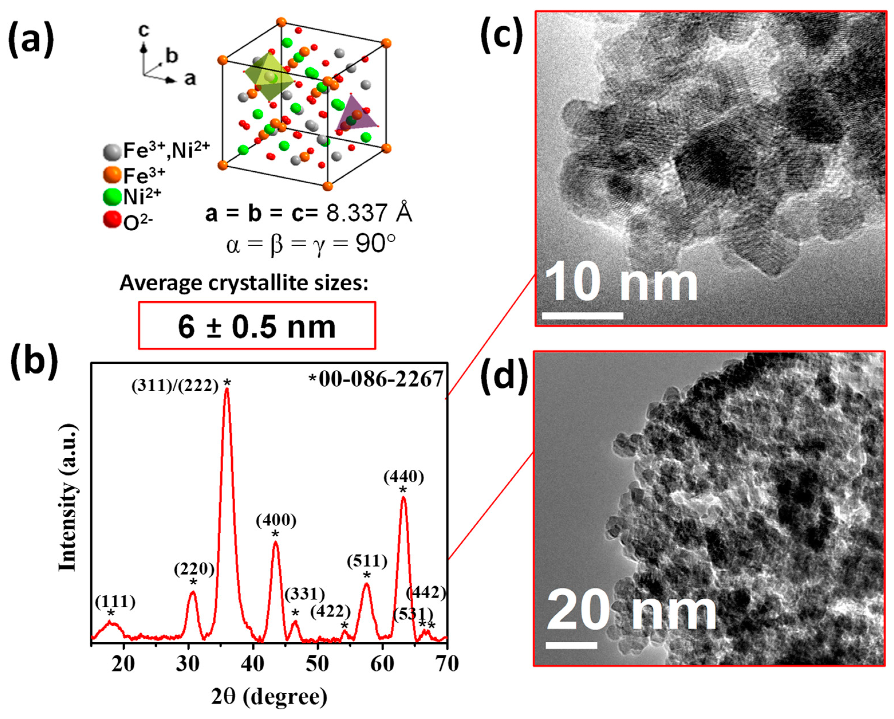
2.1. NiFe2O4NPs Characterization

All the chemical reagents, metallic salts, solvents, and polymers used in this work were purchased from commercial sources (Sigma-Aldrich, St. Louis, MO, USA). The NiFe2O4 NPs were obtained according to procedures previously reported by Rincon-Granados et al. from nickel acetylacetonate (Ni(C5H7O2)2) (95%), iron acetylacetonate (Fe(C5H7O2)3) (99.9%), and sodium hydroxide (NaOH) (97%) by a mechanochemical procedure [33]. X-ray diffraction patterns were performed at room temperature with Cu K α radiation (λ = 1.5406 Å) in a D5000 Siemens diffractometer (Bruker, Billerica, MA, USA); diffraction intensity was measured between 10° and 70° with a 2θ step of 0.01° and 0.25 s per point. The average crystal size (D) of the NPs was estimated from their diffractograms using the Debye-Scherer formula, D = κλ/βcos θ, where κ is the shape factor equal to 0.9, λ is the CuK α radiation, β is the full width at half maximum intensity (FWHM) of the selected peaks, and θ is the Bragg angle. Transmission electron micrographs (TEM) were obtained with an FEI Tecnai F20 microscope (Thermo Fisher, Waltham, MA, USA) operating at 200 kV S/TEM field emission with an X-TWIN lens and a high-brightness field emission electron gun (FEG).

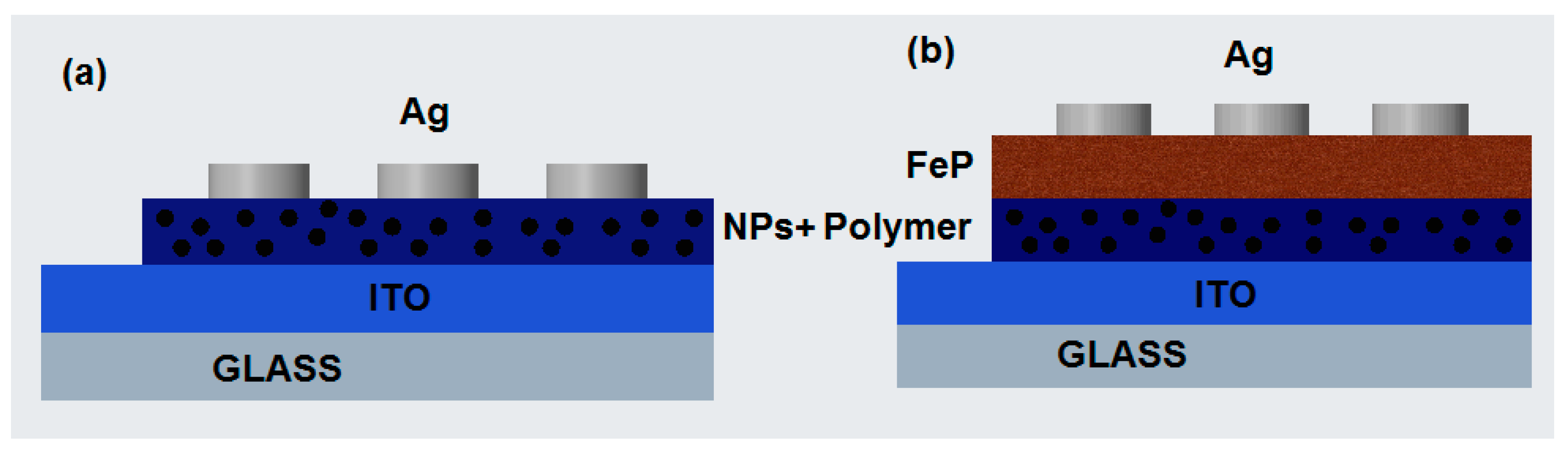
2.2. Hybrid Film Deposition

Hybrid films composed of NiFe2O4 NPs embedded in poly(3,4-ethylenedioxythiophene):poly(styrenesulfonate) (PEDOT:PSS: [C8H8O3S]n-[C6H6O2S]n) and poly(methacrylic acid methyl ester) (PMMA; [CH2C(CH3)(CO2CH3)]n) matrices were fabricated using the spin-coating technique. PEDOT:PSS and NiFe2O4 NPs, as well as PMMA and NiFe2O4 NPs, were dispersed using the G560 shaker of Scientific Industries Vortex-Genie (Bohemia, New York, USA). Dispersions at 5 wt.% of NPs were used in (i) 1 wt.% PEDOT:PSS in water or (ii) 1 wt.% PMMA in chloroform. The dispersions were deposited with a Smart Coater 200 equipment (Laurell Technologies Corporation, North Wales, PA, USA) that operated, for the PEDOT: PSS-NiFe2O4 NPs films, at a constant angular speed of 800 rpm with a time of 8 s and an acceleration of 250 rpm/s. The constant angular speed used for the PMMA-NiFe2O4 NPs films was 600 rpm with a time of 9 s and an acceleration of 250 rpm/s. Different substrates were used to support the films: Corning glass, monocrystalline silicon wafers (c-Si), and glass coated with indium tin oxide (ITO). Initially, the Corning glass and the ITO glass substrates were sequentially washed in an ultrasonic bath with dichloromethane, methanol, and acetone. The silicon substrates were washed with a “p” solution (10 mL HF, 15 mL HNO3, and 300 mL H2O) to remove surface oxide. After deposition, the films were dried at 85 °C for 2 min on a hot plate. The PEDOT:PSS-NiFe2O4 NPs films underwent a post-treatment by vapor exposure of isopropanol (IPA) and were heated at 40 °C for 10 min.

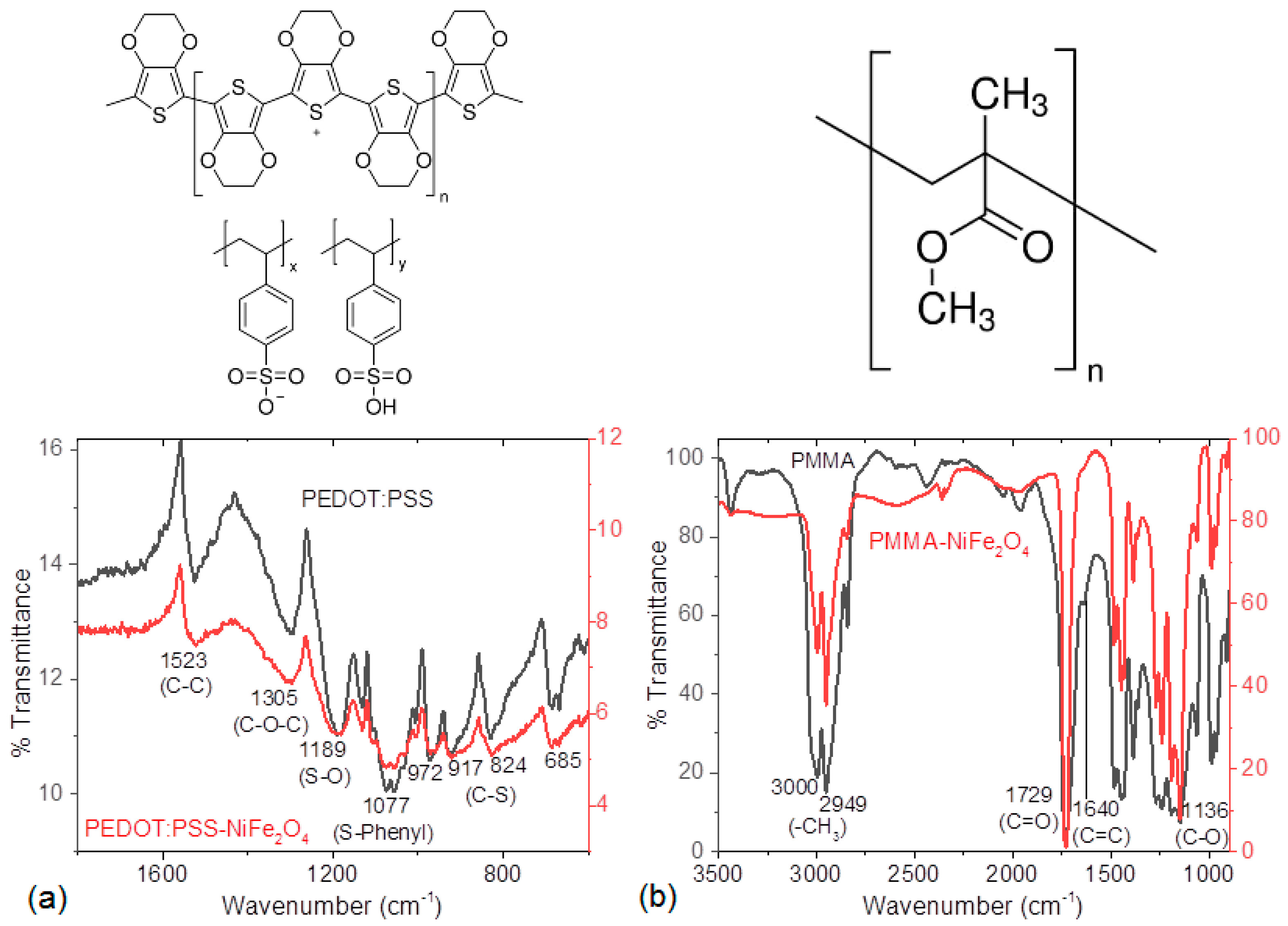
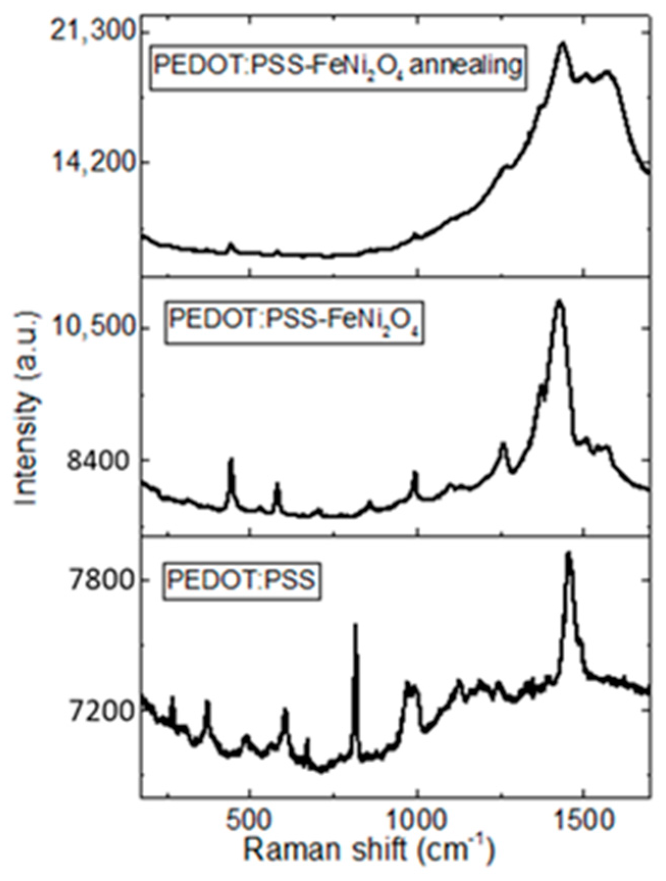
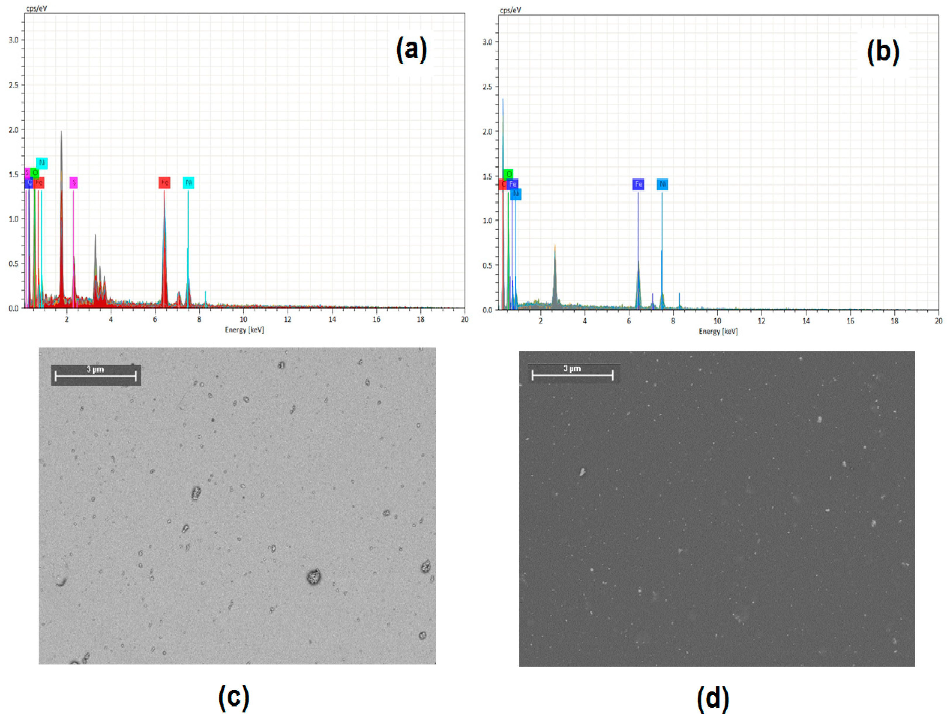
2.3. Hybrid Film Characterization

FTIR spectroscopy analysis was performed using a Nicolet iS5-FT spectrometer (Thermo Fisher Scientific Inc., Waltham, MA, USA) at a wavelength range of 4000 to 400 cm−1. Raman spectra of 100 to 900 cm−1 were acquired in a Nicolet Almega XR (Thermo Scientific Nicolet, Waltham, MA, USA) dispersive Raman spectrometer and detected by a CCD camera at 25 s and a resolution of ~4 cm−1. The excitation beam was a Nd:YVO 4532 nm laser, and the incident power on the sample was ~3 mW. The roughness, topography, thickness, and mechanical properties of the hybrid films deposited on the silicon substrate were investigated with an atomic force microscope (AFM) using an Ntegra platform (Nanosurf, Liestal, Switzerland). In order to measure film thickness, an edge of the film was initially removed from the substrate in order to have a clean area so that only the substrate would be present and thus generate a step between the film and the substrate. The AFM tip was then placed on the film surface and made to pass through it in contact mode until it touched the clean substrate [34,35]. Subsequently, the images were analyzed with the Gwyddion software platform to determine the thickness through the height difference between the highest point and the lowest point. Due to the structural difference of the films and the type of technique used for the deposit, their average thicknesses changed slightly: 7.6 μm (PEDOT:PSS), 11.1 μm (PEDOT:PSS-NiFe2O4 NPs), 6.5 μm (PMMA) and 11.7 μm (PMMA-NiFe2O4 NPs).
To study the morphology and ensure the presence of the NiFe2O4 NPs in the films deposited on the glass substrate, energy-dispersive spectroscopy (EDS) and scanning electron microscopy (SEM) were performed on a ZEISS EVO LS 10 scanning electron microscope (Carl Zeiss AG, Oberkochen, Germany) with a coupled Bruker microanalysis system (Bruker Nano GmbH, Berlin, Germany). Optical properties, absorbance, and transmittance of the hybrid films on the glass substrate were obtained using a UV–Vis 300 Unicam spectrophotometer (Thermo Fisher Scientific Inc., Waltham, MA, USA), in a wavelength range from 190 to 1100 nm. An auto-ranging picoammeter Keithley 4200-SCS-PK1 (Tektronix Inc., Beaverton, OR, USA) with a four-point probe and a lighting controller circuit from Next Robotix (Comercializadora KMox, S.A. de C.V., Mexico City, Mexico), was used to obtain the electrical properties through current–voltage (I–V) measurements of the fabricated devices, using an ITO glass substrate as the anode and silver as the cathode. Finally, to modify the behavior of the device, a 2,3,7,8,12,13,17,18-octaethyl-21H,23H-porphine iron(III) chloride (PFeCl: C36H44ClFeN4) film was deposited over PEDOT:PSS-NiFe2O4 NPs and PMMA-NiFe2O4 NPs films using a high-vacuum thermal evaporation system (Intercovamex, Morelos, Mexico). The PFeCl film was heated to 250 °C and sublimated at a vacuum pressure of 2.6 × 10⁻⁶ Torr; the deposition rate was 35.1 Å/s.

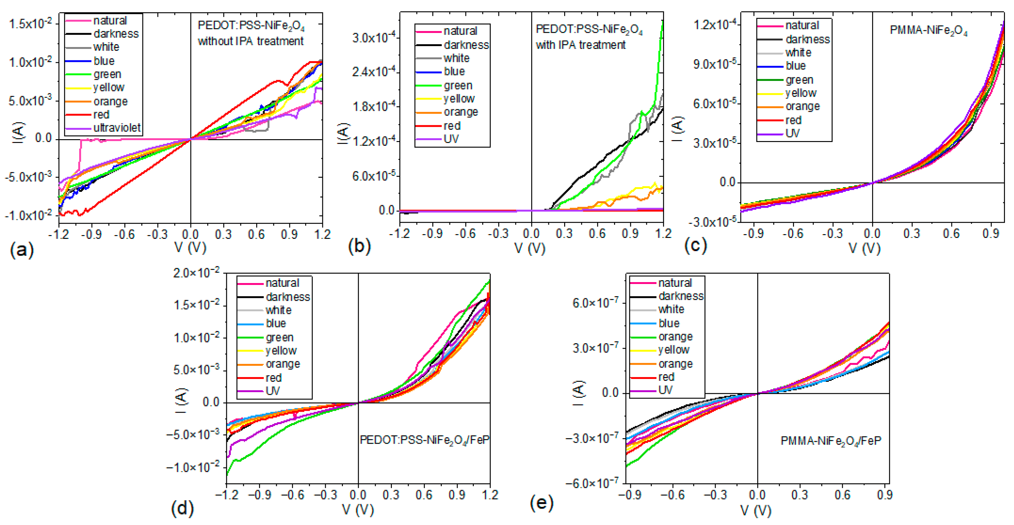
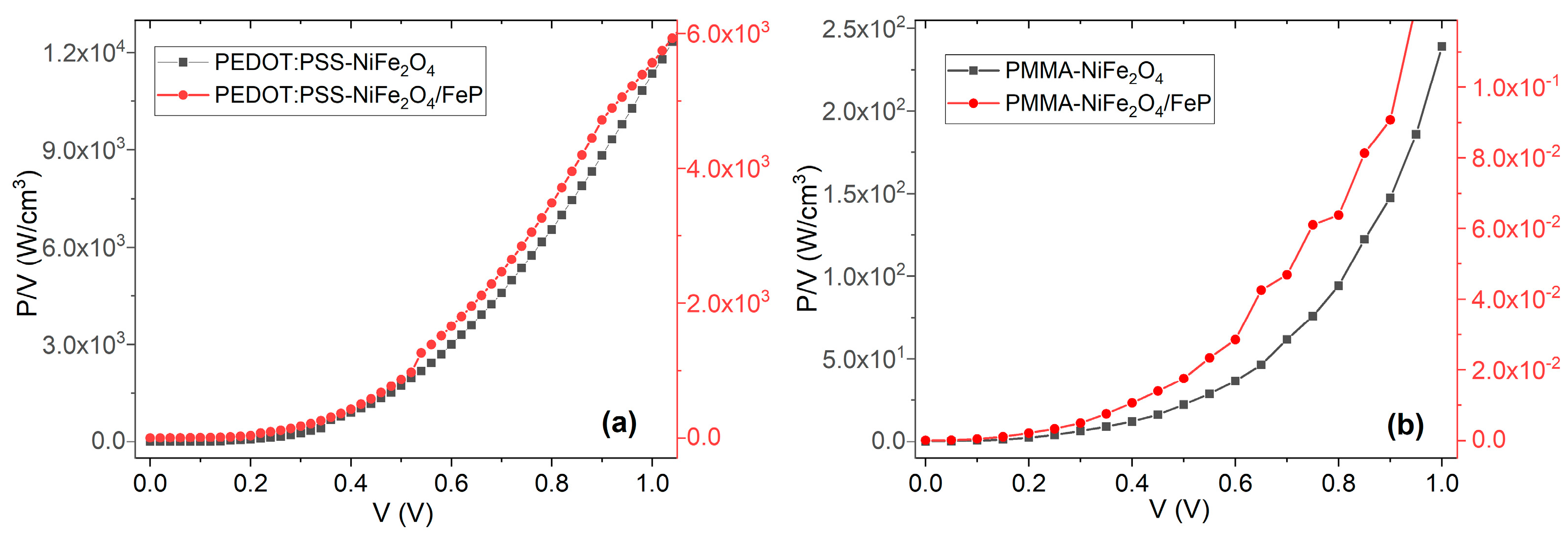
3. Results and Discussion

The NiFe2O4 NPs were characterized by powder XRD and TEM microscopy. Figure 1 shows the XRD pattern of the NiFe2O4 NPs (Figure 1a), which corresponds to an inverse spinel-type structure and a cubic phase with space group Fd-3 m and crystal lattice parameter a = 8.33 Å according to the ICDD 00-086-2267 card. No additional peaks from other faces were observed (Figure 1b). Scherrer’s equation estimated the average crystallite size at 6 ± 0.5 nm. TEM micrographs (Figure 1c,d) also corroborated the formation of nanocrystals with dimensions close to those determined from the corresponding X-ray diffraction pattern.
Hybrid films were fabricated through the spin-coating technique. After deposition, IR spectroscopy measurements of the PEDOT:PSS-NiFe2O4 NPs and PMMA-NiFe2O4 NPs films were performed in order to verify that no degradation of the polymer matrix had taken place during deposition. In Figure 2a, the spectrum of the PEDOT:PSS-NiFe2O4 NPs film shows peaks corresponding to the polymer at (i) 1523 cm−1 for the C-C bond, (ii) 1305 cm−1 for the C-O-C bond, (iii) 1077 cm−1 for the S-O bond, and (iv) 1077 cm−1 for the bond between S and the phenyl group in PEDOT:PSS; (v) the last four peaks at 972, 917, 824, and 685 cm−1 reflect C-S group stretches in PEDOT:PSS [36,37,38]. Regarding PMMA, Figure 2b shows the IR spectrum for the PMMA-NiFe2O4 NPs film. The following signals corresponding to the polymer can be observed: (i) 3000 and 2949 cm−1 for the methyl group, (ii) 1729 cm−1 for the C=O bond, (iii) 1640 cm−1 for the C=C bond, and (iv) 1136 cm−1 for the C-O bond [39]. IR spectroscopy results indicate that the polymers used as a matrix in the fabrication of the hybrid films did not undergo decomposition during the deposition process. Regarding the NPs, due to their chemical nature and resistance to organic solvents and their resistance to high temperatures, no decomposition was expected during the preparation of the hybrid films. However, their distribution in the polymeric matrix was verified later in the morphological studies of the hybrid films.
Raman spectroscopy was used to monitor the distribution of NPs in the polymeric matrix and the possible transformation of the benzoid structure to the quinoid structure of PEDOT before and after its treatment with IPA. Figure 3 shows the Raman spectra of PEDOT:PSS pristine and PEDOT:PSS-NiFe2O4 NPs films. The post-treated PEDOT:PSS-NiFe2O4 NPs film had a change in relative intensity in comparison to the PEDOT:PSS pristine film. Changes in the Raman spectral intensity confirm the interaction between the NiFe2O4 NPs and PEDOT chains; this may be caused by the redistribution of PEDOT:PSS and the NPs as a result of the IPA treatment. The increase in relative intensity for the treated film means that the PEDOT:PSS distribution becomes more uniform through the film, enhancing the detection of their main planes in the Raman spectrum. Additionally, the strongest band between 1380 and 1620 cm−1 corresponds to the Cα = Cβ symmetric stretching of the five-membered thiophene ring on the PEDOT chains [40,41,42]. The symmetric stretching vibration Cα = Cβ has a red-shifted peak when the chain structure changes from the benzoid to the quinoid form [36,37,38]. The displacement of the 1430 cm−1 signal in the spectra in Figure 3 is practically negligible, which is an indication that in this film the transformation of the PEDOT structure was not carried out. This result is relevant because the presence of NPs inhibits the transformation of PEDOT to the quinoid form; however, the post-treatment with IPA helps to improve the distribution of NPs in the polymeric matrix.
In the EDS analysis of the films after the IPA treatment, as shown in Figure 4a,b, the chemical elements corresponding to the polymer and the NPs can be observed. In both spectra, the presence of Ni and Fe is due to the NPs, and the presence of S and C in Figure 4a is due to the presence of PEDOT:PSS. The presence of O is due to the polymer as well as the NiFe2O4 NPs. As for the PMMA films, the presence of C in Figure 4b is due to the polymer and that of O is related to the NPs. SEM analysis (Figure 4c,d) was used to study the morphology of the films; a homogeneous distribution of NPs throughout the entire matrix was observed in PEDOT:PSS-NiFe2O4 NPs and PMMA-NiFe2O4 NPs. However, in the PEDOT:PSS film some NP agglomerations were observed which produced larger structures than those observed in the PMMA film. According to the EDS and SEM results, it is evident that the NiFe2O4 NPs were adequately incorporated into the polymer matrix, thus forming dispersed heterojunction films; however, a further topographic study of the films was necessary due to the important requirements in organic electronics related to the homogeneity and quality of the films needed in these devices.
The topographic characterization of the hybrid films was supplemented by means of AFM studies. Figure 5 shows the AFM images for the films of the pristine PEDOT:PSS and PMMA polymers (Figure 5a,c, respectively) and for the hybrid PEDOT:PSS-NiFe2O4 NPs and PMMA-NiFe2O4 NPs films (Figure 5b,d, respectively). In the case of the films with PEDOT:PSS, a different topography is observed in terms of the growth direction of the polymer; in the pristine film, the direction is perpendicular to the surface (~90°), and in the PEDOT:PSS-NiFe2O4 NPs film with IPA post-treatment, a preferential growth direction is observed with an angle smaller than 90°. The interaction between NiFe2O4 and PEDOT:PSS can be a decisive factor in the topography of the film because NPs can behave as nuclei around which the polymer is deposited in a preferential direction. In Table 1, the root mean square roughness (RMS) and the average roughness (Ra) are presented; RMS represents the average of the squared deviations concerning the average height of the films and is more significant than Ra, which represents the arithmetic average of the absolute values of the heights of the films. The PEDOT:PSS pristine film had a lower roughness than the PEDOT:PSS-NiFe2O4 NPs film. This result is to be expected considering that the NPs have an average crystallite size of 5 ± 0.4 nm [33] and that when they are embedded in the PEDOT:PSS matrix they increase the roughness of the film. In the case of the PMMA polymer films, the topography, RMS, and Ra changed drastically upon incorporating NiFe2O4 NPs. The presence of NPs not only increases roughness but also allows the topography to become heterogeneous, with a larger grain size. When comparing the PEDOT:PSS films with the PMMA films, it is observed that although RMS and Ra do not differ significantly, their topographies are very different from those of the PEDOT:PSS-NiFe2O4 NPs and PMMA-NiFe2O4 NPs films. PEDOT:PSS seems to have better interaction and behavior as a matrix and generates more homogeneous films than PMMA.
Regarding mechanical behavior when considering a maximum applied force of 900 N, the maximum stress (σmax), the unitary deformation (εunit), and the Knoop micro hardness (HK) were obtained by AFM and are presented in Table 1. In the case of films with PEDOT:PSS, it is observed that the presence of NiFe2O4 NPs increases the stress that the film is capable of withstanding by a factor of about 2.6 times. In the case of PMMA films, there is a very small increase in the stress that the film can withstand when introducing NiFe2O4 NPs. The above may be a result of the increase in grain size observed in the PMMA-NiFe2O4 NPs film (Figure 5d) and a deficiency of this polymer in its function as a matrix. On the other hand, HK was calculated from the length of the long penetration diagonal in the films, and according to Table 1 the values obtained are very small, although they increase with the presence of NPs. This increase is more significant in the films with PEDOT:PSS, which once again demonstrates better behavior as a matrix as post-treatment with IPA favors the interaction and distribution of NPs in the PEDOT:PSS. Finally, and as expected, it is observed that the deformation in the hybrid films is smaller than in the films with the pristine polymers; the NPs exert the function of anchoring sites that prevent the flow and deformation of the matrix. For applications in organic electronics, it is required that the films have adequate mechanical resistance and dimensional stability, which according to the results obtained is favored by incorporating the NiFe2O4 NPs in the PEDOT:PSS matrix.
The optical and electrical behavior of the hybrid films must also be evaluated to determine if they have a potential for use in device manufacturing. In order to evaluate the ability of the films to behave as transparent anodes, the transmittances of the pristine polymers and the hybrid films PEDOT:PSS-NiFe2O4 NPs and PMMA-NiFe2O4 NPs were evaluated. The spectra of Figure 6 show that the presence of NiFe2O4 NPs increases the transmittance in the hybrid films. This effect is more significant in the PMMA-NiFe2O4 NPs film, where a higher transmittance of 87% is obtained compared to the 80% that is achieved at wavelengths between 340 and 470 nm in the hybrid film with PEDOT:PSS. This result suggests the possibility of using PMMA-NiFe2O4 NPs film as a transparent anode, which could eventually replace costly or easily oxidized anodes such as ITO or FTO (fluorine-doped tin oxide), which are just some of the expensive anodes currently used. In solar cells, for example, radiation must enter the interior of the device and reach its active layer, so one of its electrodes, which is normally the anode, should be (semi)transparent to radiation. According to these results, the PMMA-NiFe2O4 NPs film is a viable option and an even better one than PEDOT:PSS, which has already been studied for this particular application [43,44,45].
If the use of hybrid films as constituents of devices in organic electronics is required, it is important to determine their optical band gap (Eg), which indicates their charge transport capability. The model by Tauc [46,47] relates the Eg of hybrid films to its photon energy () and the absorption coefficient (α) according to:
(αhν) = A( − Eg)r
In the above expression, A depends on the type of transition, r takes the value 2 for indirect electronic transitions in amorphous heterostructures, h is Planck’s constant, and ν is the frequency, which is given by:
ν = c λ
where c is the speed of light, λ is the wavelength, and α is experimentally obtained from [47]:
α = (1/d) ln (1/T)
Here, d is the film thickness as obtained from AFM and T is the transmission; the reflectivity (R) is neglected due to its low level for each film, which is caused by the presence of NPs [33,48]. The Tauc band gap is determined from the graphs of Figure 7 by plotting (αhν)1/2 versus and finding the intercept on the axis through extrapolation of the plot to (αhν)1/2 = 0. In these graphs, a similarity is observed when comparing the curves for the films of the pure PEDOT:PSS and PMMA polymers and those for their films with NiFe2O4 NPs. The Tauc bandgap value reported in Table 2 is the same for PEDOT:PSS pristine and for the PEDOT:PSS-NiFe2O4 NPs film. According to Jarząbek et al. [48], this constant value of the Tauc band gap means that the NPs do not influence conjugation in the main, rigid polymer chains. It seems that the structural changes of the composite film during the incorporation of the NPs and the post-treatment with IPA are due to the redistribution of NPs in the polymeric matrix, but the conjugation in the main PEDOT:PSS chains is preserved and the energy band gap remains constant. Regarding the band gap of the PMMA and PMMA-NiFe2O4 films, the introduction of the NPs influences the conjugation in the main chains of PMMA. The films with PMMA have the lowest Tauc gap and would therefore have a behavior resembling that of a semiconductor. The Tauc gap is a consequence of several factors related to electronic-transition processes, including defects, structural disorder, and traps. The Urbach energy (EU) can be used to determine the defects in the band gap and can be evaluated from the following equation [49,50]:
α = A a e x p h v E U
In addition to the parameters defined above, A a is a constant of the material that conforms to α at the energy gap. Figure 7c,d displays the nearly linear relationship between ln(α) and for the hybrid films. The values of EU were determined from the reciprocal of the slope from this linear relation and have been recorded in Table 2. The Urbach energy corresponds to the width of the band tail, which is related to localized states within the energy gap, possibly caused by structural defects [48]. As a reference, the value of EU is zero in a perfect semiconductor [51]. The highest EU belongs to the PEDOT:PSS-NiFe2O4 NPs film, and the lowest EU belongs to the PMMA-NiFe2O4 NPs film. From the values of Eg and EU, it is understood that the PMMA film shows the best semiconducting behavior, which is a required feature in organic electronics. In addition to performing as a transparent anode (see Figure 6b), it also has the potential for use as an active layer. The behavior of the NPs and their effect on the optical properties of the films depend on the matrix in which they are embedded. In the case of films with PEDOT:PSS, the presence of NPs slightly increases the value of EU; however, the value of EU for the PMMA pristine matrix is higher than that obtained with the NiFe2O4 NPs. Finally, it is important to consider that the values obtained for EU are in the same range as those for some inorganic semiconductor films, such as Bi2S3 (0.26 eV) and Bi2−xCrxS3 (0.35 eV) [51]. They are lower than for some hybrid films, such as PVOH (polyvinyl alcohol) film embedded with Bi-nanoparticles (0.604 eV) [52], while they are bigger than for hybrid films with poly(3-hexylthiophene) (0.11–0.17 eV) [48]. Unfortunately, there is not much information available about the EU values for hybrid films with FeNi2O4 NPs in a polymeric matrix.
To improve the semiconducting behavior of the hybrid films, a PFeCl layer was deposited by evaporation under high vacuum, forming a planar heterojunction on the polymer-NiFe2O4 NPs films. The porphine film was added as an electron transport layer. According to Figure 8, the presence of PFeCl film with a low band gap could favor a semiconductor behavior in the/polymer-NiFe2O4 NPs/PFeCl/system. The narrow band gap can be attributed to (i) FePCl optical properties, (ii) their proper interaction with the components of the hetero-junction system [23], and (iii) heat-induced movements of polymer particles [48,53]. During the deposition of the PFeCl film by the high-vacuum evaporation technique, the porphine molecules in a gaseous state are deposited on the polymer-NiFe2O4 NPs film, and at this site they turn to the solid state. While this deposition occurs, the polymer-NiFe2O4 NPs film heats up, thus enlarging the free volume and decreasing the order between polymer chains, which causes a blue shift and a decrease in the band gap [48,53].
To evaluate the electrical behavior in the heterostructures, Figure 9 shows the schemes of the devices manufactured for the polymer-NiFe2O4 NPs (Figure 9a) and/polymer-NiFe2O4 NPs/PFeCl/(Figure 9b) devices. Figure 10a,b shows the behavior of the devices with PEDOT:PSS before and after performing the IPA treatment. When comparing the graphs, a marked difference between the two is observed as a result of the rearrangement between the NPs and the polymer after post-treatment. Before the treatment, an ohmic behavior is observed in the device under the different lighting conditions; in addition, there is a tendency towards the ambipolarity of the device. However, under most lighting conditions and at V > 0.4 V, the device interferes with the current flow, probably because the NPs are not perfectly embedded in the polymeric matrix. After treatment, the behavior of this device changes completely; according to Raman spectroscopy, the post-treatment with IPA changes the distribution of NPs in the polymeric matrix, and this influences charge transport. When analyzing and comparing the results obtained for the glass/ITO/polymer-NiFe2O4 NPs/Ag devices with PEDOT:PSS (see Figure 10b) and PMMA (see Figure 10c), it is observed that the maximum current carried is of the same order of magnitude in the two devices; the device with PEDOT:PSS is affected by the type of radiation that falls on it. The maximum current carried is generated with wavelength illumination corresponding to green light, while a current reduction occurs under blue and violet lighting or under natural lighting conditions. The behavior of this device in darkness also changes, and this result could be an indication of photovoltaic properties that may be studied in the future. The type and position of the anode and cathode, as well as the direction of current flow, determine device behavior; at negative voltages, the behavior is practically that of an insulator, while at positive voltages, and despite presenting interference in charge transport, the behavior is ohmic. On the other hand, in the device with PMMA, there is no significant influence on charge transport when lighting conditions change; the behavior is mostly ohmic, although it is somewhat similar to that of a Schottky diode. In this device, there is no ambipolar behavior; nevertheless, current flow is continuous and without barriers or interference generated by the NPs-polymer interface.
The incorporation of the porphine film generates a significant change in the electrical behavior of the devices, which can be considered ambipolar (see Figure 10c,d). Transported current increases by two orders of magnitude in glass/ITO/PEDOT:PSS-NiFe2O4 NPs/Ag devices relative to glass/ITO/PEDOT:PSS-NiFe2O4 NPs/PFeCl/Ag devices. On the other hand, through the incorporation of the porphine film, the electric current decreases by three orders of magnitude in the glass/ITO/PMMA-NiFe2O4 NPs/Ag/device relative to the glass/ITO/PMMA-NiFe2O4 NPs/PFeCl/Ag/device. The devices with the PFeCl film show a behavior resembling that of a Schottky diode, and there are no significant changes when irradiating them with different wavelengths. Finally, it is important to mention that the device with the highest current is glass/ITO/PEDOT:PSS-NiFe2O4 NPs/PFeCl/Ag/. From these results, it can be seen that the rectifying behavior of the devices without the porphine film acquires an ohmic character with the addition of PFeCl. In the PEDOT device, this also leads to an increased electric current, whereas the PMMA device undergoes a reduction in current, which can be attributed to changes in the local electronic structure at the interface between the polymer and the porphine films.
Figure 11 shows the graphs of power per unit volume with respect to (positive) voltage applied to the devices. Device volumes are 3.78 × 10⁻⁷ and 2.62 × 10⁻⁶ cm3 for the glass/ITO/PEDOT:PSS-NiFe2O4 NPs/Ag and glass/ITO/PEDOT:PSS-NiFe2O4 NPs/PFeCl/Ag devices, respectively, and 4.21 × 10⁻⁷ and 2.98 × 10⁻⁶ cm3 for the glass/ITO/PMMA-NiFe2O4 NPs/Ag and glass/ITO/PMMA-NiFe2O4 NPs/PFeCl/Ag devices, respectively. As expected, there is a roughly exponential shape in the power density versus voltage graphs that can be associated to the rectifier- and ohmic-like behaviors of the devices. It is interesting to notice the discontinuous changes in slope in the graph of the PMMA-based device, which are possibly due to charge-storage effects at the interfaces between the nanoparticles and the matrix.

4. Conclusions

Hybrid films of NiFe2O4 NPs in PEDOT:PSS and PMMA were obtained by the spin-coating technique. The NPs positively affect the films’ mechanical properties by increasing the maximum stress they can withstand and their HK hardness. The behavior of the NPs and their effect on the optical properties of the films depend on the matrix in which they are embedded. Another important aspect of the use of NPs is their effect on the electrical behavior of glass/ITO/polymer-NiFe2O4 NPs/Ag devices, which changes depending on the matrix. In the case of PEDOT:PSS, IPA treatment influences charge transport, and the current carried in its device depends on the wavelength with which it is irradiated. In the case of the device with the PMMA matrix, an ambipolar behavior occurs which is independent of the light that falls on it. NiFe2O4 NPs may be considered for use in organic electronics applications; when used as film reinforcement with PEDOT:PSS and PMMA matrices, they enhance their mechanical, optical, and electrical properties. The addition of a porphine layer to devices based on these materials adds an ohmic component to their mostly rectifying behavior.

Author Contributions

Conceptualization, M.E.S.V. and A.R.V.-O.; methodology, M.E.S.V., M.J.A.R., A.R.V.-O., K.L.R.-G. and R.Y.S.-B.; software, M.E.S.V. and M.J.A.R.; validation, M.E.S.V., M.J.A.R., J.R.Á.B., A.R.V.-O., K.L.R.-G. and R.Y.S.-B.; formal analysis, M.E.S.V., M.J.A.R. and A.R.V.-O.; investigation, M.J.A.R. and K.L.R.-G.; resources, M.E.S.V., J.R.Á.B. and A.R.V.-O.; data curation, M.E.S.V., M.J.A.R., A.R.V.-O., K.L.R.-G. and R.Y.S.-B.; writing—original draft preparation, M.E.S.V., M.J.A.R., J.R.Á.B., A.R.V.-O. and K.L.R.-G.; writing—review and editing, M.E.S.V., M.J.A.R., J.R.Á.B., A.R.V.-O. and K.L.R.-G.; visualization, M.J.A.R., J.R.Á.B. and K.L.R.-G.; supervision, M.E.S.V. and A.R.V.-O.; project administration, M.E.S.V.; funding acquisition, M.E.S.V. and A.R.V.-O. All authors have read and agreed to the published version of the manuscript.

Funding

María Elena Sánchez Vergara gratefully acknowledges financial support from Consejo Mexiquense de Ciencia y Tecnología, Financiamiento para investigación de mujeres científicas: EDOMÉX-FICDTEM-2022-01, Project 64. Karen L. Rincón-Granados gratefully acknowledges CONACYT for a Ph.D. scholarship. América Vázquez-Olmos gratefully acknowledges the support for this research given by the UNAM-PAPIIT IN113423.

Data Availability Statement

Data is contained within the article.

Acknowledgments

The authors are grateful for the technical support of Vicente Garibay-Febles, Fernando Gibran Mendoza López, Valeria López Valenzuela, and Montserrat Mendoza Felix.

Conflicts of Interest

The authors declare no conflict of interest.

References

  1. Sharifi, I.; Shokrollahi, H.; Amiri, S. Ferrite-based magnetic nanofluids used in hyperthermia applications. J. Magn. Magn. Mater. 2012, 324, 903–915. [Google Scholar] [CrossRef]
  2. Matsui, I. Nanoparticles for Electronic Device Applications: A Brief Review. J. Chem. Eng. Jpn. 2005, 38, 535–546. [Google Scholar] [CrossRef]
  3. Park, M.; Seo, S.; Lee, I.S.; Jung, J.H. Ultraefficient separation and sensing of mercury and methylmercury ions in drinking water by using aminonaphthalimide-functionalized Fe3O4@SiO2 core/shell magnetic nanoparticles. Chem. Commun. 2010, 46, 4478–4480. [Google Scholar] [CrossRef] [PubMed]
  4. Viltužnik, B.; Košak, A.; Zub, Y.L.; Lobnik, A. Removal of Pb(II) ions from aqueous systems using thiol-functionalized cobaltferrite magnetic nanoparticles. J. Sol-Gel Sci. Technol. 2013, 68, 365–373. [Google Scholar] [CrossRef]
  5. Tartaj, P.; Morales, M.P.; Gonzalez, T.; Veintemillas, S.; Serna, C.J. The iron oxides strike back: From biomedical applications to energy storage devices and photoelectrochemical water splitting. Adv. Mater. 2011, 23, 5243–5249. [Google Scholar] [CrossRef] [PubMed]
  6. Goya, G.F.; Grazú, V.; Ibarra, M.R. Magnetic Nanoparticles for Cancer Therapy. Curr. Nanosci. 2008, 4, 1–16. [Google Scholar] [CrossRef]
  7. Laurent, S.; Forge, D.; Port, M.; Roch, A.; Robic, C.; Elst, L.V.; Muller, R.N. Magnetic Iron Oxide Nanoparticles: Synthesis, Stabilization, Vectorization, Physicochemical Characterizations, and Biological Applications. Chem. Rev. 2010, 108, 2064–2110. [Google Scholar] [CrossRef] [PubMed]
  8. Lazarević, Z.Ž.; Jovalekić, Č.; Milutinović, A.; Romčević, M.; Romčević, N.Ž. Preparation and characterization of nano ferrites. Acta Phys. Pol. A 2012, 121, 682–686. [Google Scholar] [CrossRef]
  9. Sabale, S.; Jadhav, V.; Khot, V.; Zhu, X.; Xin, M.; Chen, H. Superparamagnetic MFe2O4 (M = Ni, Co, Zn, Mn) nanoparticles: Synthesis, characterization, induction heating and cell viability studies for cancer hyperthermia applications. J. Mater. Sci. Mater. Med. 2015, 26, 127. [Google Scholar] [CrossRef]
  10. Castellanos-Rubio, I.; Insausti, M.; Garaio, E.; Gil de Mauro, I.; Plazaola, F.; Rojo, T.; Lezama, L. Fe3O4 nanoparticles prepared by the seeded-growth route for hyperthermia: Electron magnetic resonance as a key tool to evaluate size distribution in magnetic nanoparticles. Nanoscale 2014, 6, 7542–7552. [Google Scholar] [CrossRef]
  11. Obaidat, I.M.; Issa, B.; Haik, Y. Magnetic Properties of Magnetic Nanoparticles for Efficient Hyperthermia. Nanomaterials 2015, 5, 63–89. [Google Scholar] [CrossRef]
  12. Diodati, S.; Pandolfo, L.; Caneschi, A.; Gialanella, S.; Gross, S. Green and low temperature synthesis of nanocrystalline transition metal ferrites by simple wet chemistry routes. Nano Res. 2014, 7, 1027–1042. [Google Scholar] [CrossRef]
  13. Galvão, W.S.; Neto, D.M.A.; Freire, R.M.; Fechine, P.B.A. Super-paramagnetic Nanoparticles with Spinel Structure: A Review of Synthesis and Biomedical Applications. Solid State Phenom. 2016, 241, 139–176. [Google Scholar] [CrossRef]
  14. Jacob, J.; Khadar, M.A. Investigation of mixed spinel structure of nanostructured nickel ferrite. J. Appl. Phys. 2010, 107, 114310. [Google Scholar] [CrossRef]
  15. Valenzuela, R. Novel Applications of Ferrites. Phys. Res. Int. 2012, 2012, 591839. [Google Scholar] [CrossRef]
  16. Seyyed Ebrahimi, S.A.; Azadmanjiri, J. Evaluation of NiFe2O4 ferrite nanocrystalline powder synthesized by a sol–gel auto-combustion method. J. Non-Cryst. Solids 2007, 353, 802–804. [Google Scholar] [CrossRef]
  17. Rashad, M.M.; Fouad, O.A. Synthesis and characterization of nano-sized nickel ferrites from fly ash for catalytic oxidation of CO. Mater. Chem. Phys. 2005, 94, 365–370. [Google Scholar] [CrossRef]
  18. Lazarević, Z.Ž.; Jovalekić, Č.; Milutinović, A.; Sekulić, D.; Slankamenac, M.; Romčević, M.; Romčević, N.Ž. Study of NiFe2O4 and ZnNiFe2O4 Spinel Ferrites Prepared by Soft Mechanochemical Synthesis. Ferroelectrics 2013, 448, 1–11. [Google Scholar] [CrossRef]
  19. Brook, R.J.; Kingery, W.D. Nickel Ferrite Thin Films: Microstructures and Magnetic Properties. J. Appl. Phys. 1967, 38, 3589–3594. [Google Scholar] [CrossRef]
  20. Nathani, H.; Misra, R.D.K. Surface effects on the magnetic behavior of nanocrystalline nickel ferrites and nickel ferrite-polymer nanocomposites. Mater. Sci. Eng. B 2004, 113, 228–235. [Google Scholar] [CrossRef]
  21. Poudel, M.B.; Awasti, G.P.; Kim, H.J. Novel insight into the adsorption of Cr(VI) and Pb(II) ions by MOF derived Co-Al layered double hydroxide @hematite nanorods on 3D porous carbon nanofiber network. Chem. Eng. J. 2021, 417, 129312. [Google Scholar] [CrossRef]
  22. Poudel, M.B.; Kim, H.J. Confinement of Zn-Mg-Al-layered double hydroxide and α-Fe2O3 nanorods on hollow porous carbon nanofibers: A free-standing electrode for solid-state symmetric supercapacitors. Chem. Eng. J. 2022, 429, 132345. [Google Scholar] [CrossRef]
  23. Poudel, M.B.; Kim, H.J. Synthesis of Conducting Bifunctional Polyaniline@Mn-TiO2 Nanocomposites for Supercapacitor Electrode and Visible Light Driven Photocatalysis. Catalysts 2020, 10, 546. [Google Scholar] [CrossRef]
  24. Venkatesan, R.; Maideen, S.M.T.S.K.; Chandhiran, S.; Kushvaha, S.S.; Sagadevan, S.; Venkatachalapathy, V.; Mayandi, J. Fabrication and Characterization of Si/PEDOT:PSS-Based Heterojunction Solar Cells. Electronics 2022, 11, 4145. [Google Scholar] [CrossRef]
  25. Catania, F.; Oliveira, H.S.; Lugoda, P.; Cantarella, G.; Münzenrieder, N. Thin-film electronics on active substrates: Review of materials, technologies and applications. J. Phys. D Appl. Phys. 2022, 55, 323002. [Google Scholar] [CrossRef]
  26. Zidan, H.M.; Abu-Elnader, M. Structural and optical properties of pure PMMA and metal chloride-doped PMMA films. Phys. B Condens. Matter 2005, 355, 308–317. [Google Scholar] [CrossRef]
  27. Kumaresan, Y.; Lee, R.; Lim, N.; Pak, Y.; Kim, H.; Kim, W.; Jung, G.Y. Extremely flexible indium-gallium-zinc oxide (IGZO) based electronic devices placed on an ultrathin poly(methyl methacrylate) (PMMA) substrate. Adv. Electron. Mater. 2018, 4, 1800167. [Google Scholar] [CrossRef]
  28. Hwang, S.W.; Song, J.K.; Huang, X.; Cheng, H.; Kang, S.K.; Kim, B.H.; Kim, J.H.; Yu, S.; Huang, Y.; Rogers, J.A. High-performance biodegradable/transient electronics on biodegradable polymers. Adv. Mater. 2014, 26, 3905–3911. [Google Scholar] [CrossRef]
  29. Hwang, S.W.; Huang, X.; Seo, J.H.; Song, J.K.; Kim, S.; Hage-Ali, S.; Chung, H.J.; Tao, H.; Omenetto, F.G.; Ma, Z.; et al. Materials for bioresorbable radio frequency electronics. Adv. Mater. 2013, 25, 3526–3531. [Google Scholar] [CrossRef]
  30. Zhang, B.; Sun, J.; Katz, H.E.; Fang, F.; Opila, R.L. Promising Thermoelectric Properties of Commercial PEDOT:PSS Materials and Their Bi2Te3 Powder Composites. Appl. Mater. Interfaces 2010, 2, 3170–3178. [Google Scholar] [CrossRef]
  31. Pasha, A.; Khasim, S. Highly conductive organic thin films of PEDOT–PSS: Silver nanocomposite treated with PEG as a promising thermo-electric material. J. Mater. Sci.-Mater. 2020, 31, 9185–9195. [Google Scholar] [CrossRef]
  32. Singh, V.; Kumar, T. Study of modified PEDOT:PSS for tuning the optical properties of its conductive thin films. J. Sci.-Adv. Mater. Dev. 2019, 4, 538–543. [Google Scholar] [CrossRef]
  33. Rincón, K.L.; Vázquez, A.R.; Rodríguez, A.P.; Vega, A.; Ruiz, F.; Garibay, V.; Ximénez, L.A. Facile solid-state synthesis and study in vitro of the antibacterial activity of NiO and NiFe2O4 nanoparticles. Materialia 2021, 15, 100955. [Google Scholar] [CrossRef]
  34. Grzywacz, H.; Milczarek, M.; Jenczyk, P.; Dera, W.; Michałowski, M.; Jarząbek, D.M. Quantitative measurement of nanofriction between PMMA thin films and various AFM probes. Measurement 2021, 168, 108267. [Google Scholar] [CrossRef]
  35. Hernández, I. Determinación del Grosor de Una película Delgada Mediante la Combinación de Micro-Interferometría Óptica y Análisis Digital de Imágenes (Dissertation); Benemérita Universidad Autónoma de Puebla: 2019. Available online: https://repositorioinstitucional.buap.mx/bitstream/handle/20.500.12371/4668/887319TL.pdf?sequence=1 (accessed on 30 March 2023).
  36. Yoo, D.; Kim, J.; Kim, J.H. Direct synthesis of highly conductive poly(3,4-ethylenedioxythiophene):poly(4-styrenesulfonate) (PEDOT:PSS)/graphene composites and their applications in energy harvesting systems. Nano Res. 2014, 7, 717–730. [Google Scholar] [CrossRef]
  37. Rattana, T.; Chaiyakun, S.; Witit-anuna, N.; Nuntawong, N.; Chindaudom, P.; Oaew, S.; Kedkeaw, C.; Limsuwan, P. Preparation and characterization of graphene oxide nanosheets. Procedia Eng. 2012, 32, 759–764. [Google Scholar] [CrossRef]
  38. Soltani-kordshuli, F.; Zabihi, F.; Eslamian, M. Graphene-doped PEDOT:PSS nanocomposite thin films fabricated by conventional and substrate vibration-assisted spray coating (SVASC). Eng. Sci. Technol. Int. J. 2016, 19, 1216–1223. [Google Scholar] [CrossRef]
  39. James, F.; Da Cunha, L.; Pimenta, L.G.; de Oliveira, V.; Prado, M.H.; Da Mota, L.F.; Vieira, M.F. Poly (Methyl Methacrylate)-SiC Nanocomposites Prepared Through in Situ Polymerization. Mat. Res. 2018, 21, e20180086. [Google Scholar] [CrossRef]
  40. Ouyang, J.; Chu, C.W.; Chen, F.C.; Xu, Q.; Yang, Y. High-conductivity poly (3, 4-ethylenedioxythiophene): Poly (styrene sulfonate) film and its application in polymer optoelectronic devices. Adv. Funct. Mat. 2005, 15, 203–208. [Google Scholar] [CrossRef]
  41. Yeon, C.; Kim, G.; Lim, J.W.; Yun, S.J. Highly conductive PEDOT: PSS treated by sodium dodecyl sulfate for stretchable fabric heaters. RSC Adv. 2017, 7, 5888–5897. [Google Scholar] [CrossRef]
  42. Garreau, S.; Duvail, J.L.; Louarn, G. Spectroelectrochemical studies of poly (3, 4-ethylenedioxythiophene) in aqueous medium. Synth. Met. 2001, 125, 325–329. [Google Scholar] [CrossRef]
  43. Na, S.I.; Kim, S.S.; Jo, J.; Kim, D.Y. Efficient and Flexible ITO-Free Organic Solar Cells Using Highly Conductive Polymer Anodes. Adv. Mater. 2008, 20, 4061–4067. [Google Scholar] [CrossRef]
  44. Hau, S.K.; Yip, H.L.; Zou, J.; Jen, A.K.Y. Indium tin oxide-free semi-transparent inverted polymer solar cells using conducting polymer as both bottom and top electrodes. Org. Electron. 2009, 10, 1401–1407. [Google Scholar] [CrossRef]
  45. Zhou, Y.; Zhang, F.; Tvingstedt, K.; Barrau, S.; Li, F.; Tian, W.; Inganäs, O. Investigation on polymer anode design for flexible polymer solar cells. Appl. Phys. Lett. 2008, 92, 233308. [Google Scholar] [CrossRef]
  46. Tauc, J. Optical properties and electronic structure of amorphous Ge and Si. Mater. Res. Bull. 1968, 3, 37–46. [Google Scholar] [CrossRef]
  47. Tauc, J.; Menth, A. States in the gap. J. Non-Cryst. Solids 1972, 8, 569–585. [Google Scholar] [CrossRef]
  48. Jarząbek, B.; Nitschke, P.; Hajduk, B.; Domański, M.; Bednarski, H. In situ thermo-optical studies of polymer:fullerene blendfilms. Polym. Test. 2020, 88, 106573. [Google Scholar] [CrossRef]
  49. Al-Ghamdi, S.A.; Hamdalla, T.A.; Darwish, A.A.A.; Alzahrani, A.O.M.; El-Zaidia, E.F.M.; Alamrani, N.A.; Elblbesy, M.A.; Yahia, I.S. Preparation, Raman Spectroscopy, Surface Morphology and Optical Properties of TiPcCl2 Nanostructured Films: Thickness Effect. Opt. Quant. Electron. 2021, 53, 514. [Google Scholar] [CrossRef]
  50. Ghanem, M.G.; Badr, Y.; Hameed, T.A.; Marssi, M.E.; Lahmar, A.; Wahab, H.A.; Battisha, I.K. Synthesis and characterization of undoped and Er-doped ZnO nano-structure thin films deposited by sol-gel spin coating technique. Mater. Res. Express 2019, 6, 085916. [Google Scholar] [CrossRef]
  51. Fazal, T.; Iqbal, S.; Shah, M.; Ismail, B.; Shaheen, N.; Alrbyawi, H.; Al-Anazy, M.M.; Elkaeed, E.B.; Somaily, H.H.; Pa-shameah, R.A.; et al. Improvement in Optoelectronic Properties of Bismuth Sulphide Thin Films by Chromium Incorporation at the Orthorhombic Crystal Lattice for Photovoltaic Applications. Molecules 2022, 27, 6419. [Google Scholar] [CrossRef]
  52. Alí, H.E.; Yahia, I.S.; Algarni, H.; Khairy, Y. Enhancing the optical absorption, conductivity, and nonlinear parameters of PVOH films by Bi-doping. New J. Phys. 2021, 23, 043001. [Google Scholar] [CrossRef]
  53. Wang, T.; Pearson, A.J.; Lidzey, D.G.; Jones, R.A.L. Evolution of structure, optoelectronic properties, and device performance of polythiophene: Fullerene solar cells during thermal annealing. Adv. Funct. Mater. 2011, 21, 1383–1390. [Google Scholar] [CrossRef]
Figure 1. (a) Scheme of the crystalline structure of NiFe2O4, (b) X-ray diffraction pattern of the NiFe2O4 nanopowder, the asterisks correspond to the crystallographic planes reported on card 00-086-226, and (c,d) its corresponding TEM micrographs.
Nanomaterials 13 01525 g001
Figure 2. Structure and IR spectra of (a) PEDOT:PSS and (b) PMMA films.
Nanomaterials 13 01525 g002
Figure 3. Raman spectra of the PEDOT:PSS film and the PEDOT:PSS-NiFe2O4 NPs film before and after the IPA post-treatment.
Nanomaterials 13 01525 g003
Figure 4. EDS microanalysis of (a) PEDOT:PSS-NiFe2O4 NPs and (b) PMMA-NiFe2O4 NPs films. SEM photomicrographs at 250× of (c) PEDOT:PSS-NiFe2O4 NPs and (d) PMMA-NiFe2O4 NPs films.
Nanomaterials 13 01525 g004
Figure 5. AFM images of (a) PEDOT:PSS, (b) PEDOT:PSS-NiFe2O4 NPs, (c) PMMA, and (d) PMMA-NiFe2O4 NPs films.
Nanomaterials 13 01525 g005
Figure 6. Spectral behavior of the transmittance for (a) PEDOT:PSS and (b) PMMA pristine and hybrid films.
Nanomaterials 13 01525 g006
Figure 7. Variation of (αhν)1/2 with for hybrid films of (a) PEDOT:PSS and (b) PMMA. Variation of ln(α) with for hybrid films of (c) PEDOT:PSS and (d) PMMA.
Nanomaterials 13 01525 g007
Figure 8. Variation of (αhν)1/2 with for hybrid films with a PFeCl layer.
Nanomaterials 13 01525 g008
Figure 9. Device scheme for (a) glass/ITO/polymer-NiFe2O4 NPs/Ag and (b) glass/ITO/polymer-NiFe2O4 NPs/PFeCl/Ag devices.
Nanomaterials 13 01525 g009
Figure 10. I-V curves from (ac) glass/ITO/polymer-NiFe2O4 NPs/Ag and (d,e) glass/ITO/polymer-NiFe2O4 NPs/PFeCl/Ag devices under different lighting conditions.
Nanomaterials 13 01525 g010
Figure 11. P-V curves from (a) PEDOT:PSS and (b) PMMA devices under natural lighting conditions.
Nanomaterials 13 01525 g011
Table 1. Roughness and mechanical parameters of polymeric and hybrid films.
FilmRMS (nm)Ra (nm)σmax (MPa)HKmaxεunit
PEDOT:PSS2.972.2710.80.0390.95
PEDOT:PSS-NiFe2O4 NPs19.9315.01280.1030.92
PMMA3.092.248.060.0290.95
PMMA-NiFe2O4 NPs18.6513.328.20.0300.91
Table 2. Optical band gap and Urbach energy of PEDOT:PSS and PMMA hybrid films.
SampleEg (eV)EU (eV)
PEDOT:PSS3.890.318
PEDOT:PSS-NiFe2O4 NPs3.890.331
PMMA3.750.298
PMMA-NiFe2O4 NPs3.810.244
Disclaimer/Publisher’s Note: The statements, opinions and data contained in all publications are solely those of the individual author(s) and contributor(s) and not of MDPI and/or the editor(s). MDPI and/or the editor(s) disclaim responsibility for any injury to people or property resulting from any ideas, methods, instructions or products referred to in the content.

