
Efficient Charge Transfer in MAPbI3 QDs/TiO2 Heterojunctions for High-Performance Solar Cells


Abstract
:
1. Introduction
2. Materials and Methods
2.1. Materials
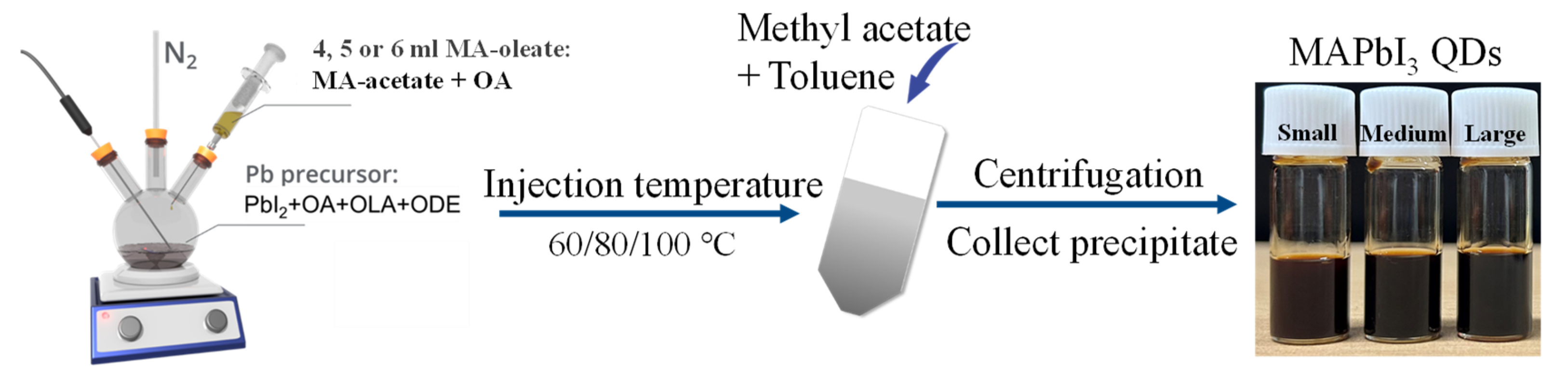
2.2. Colloidal Synthesis of MAPbI3 Quantum Dots (QDs)
2.3. Fabrication of the QDs/MOs Heterojunction
2.4. Fabrication of the MAPbI3 QD Planar Heterojunction Solar Cells
2.5. Characterization
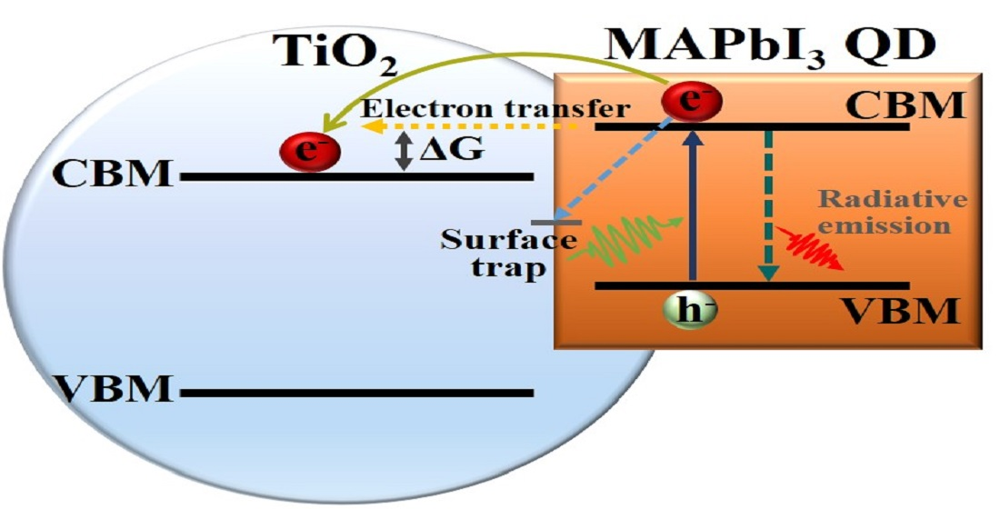
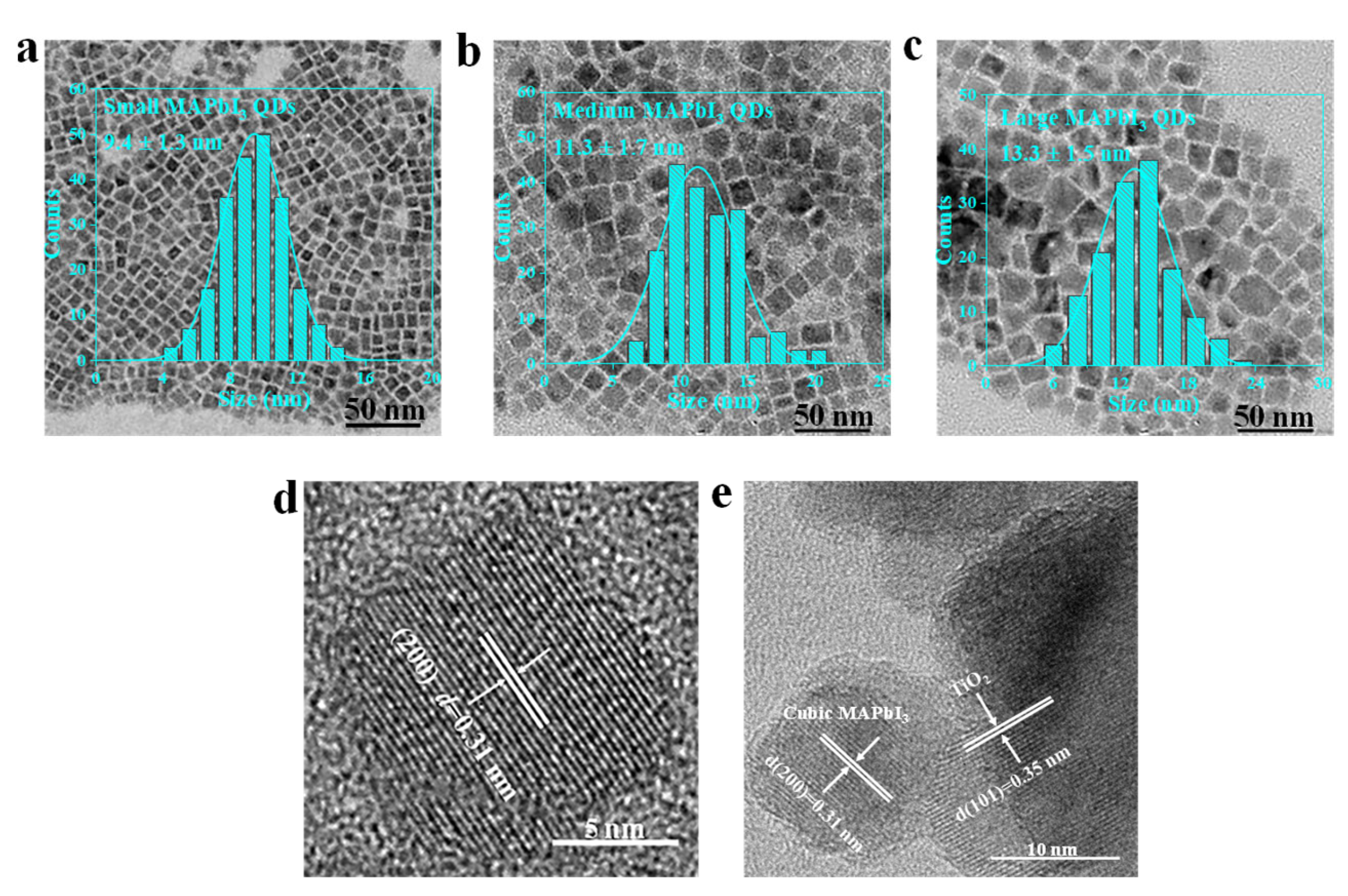
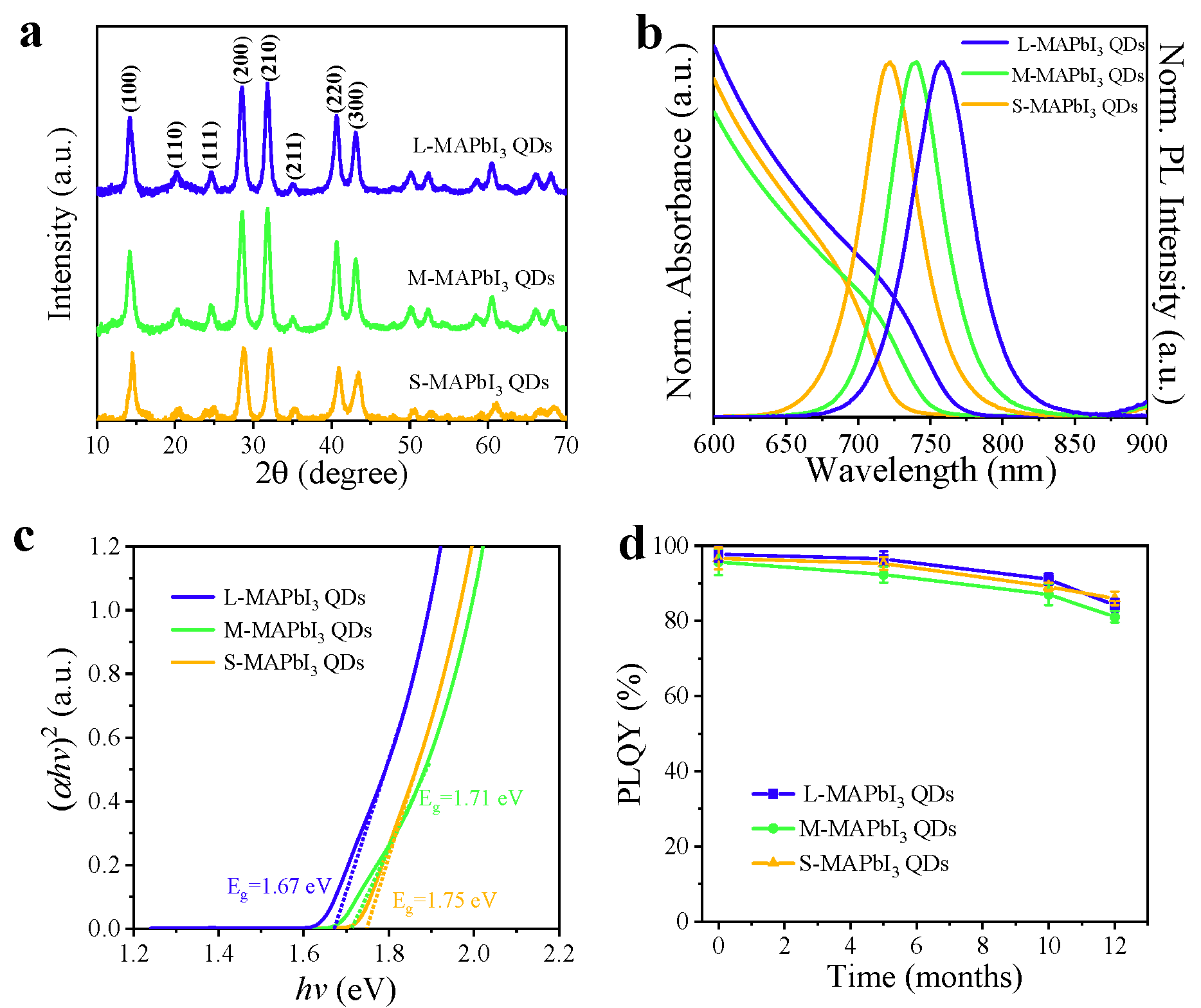
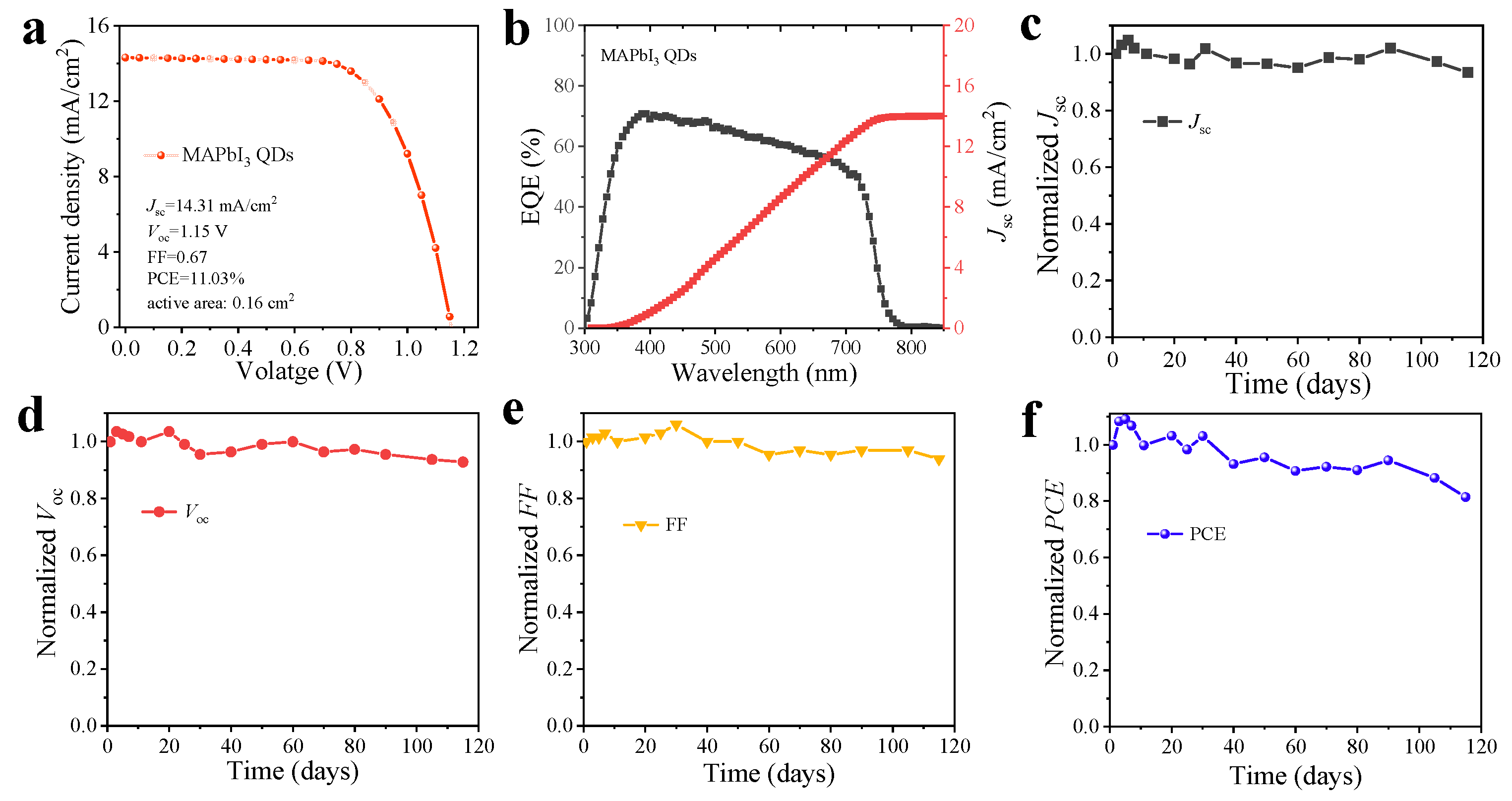
3. Results and Discussion
4. Conclusions
Author Contributions
Funding
Data Availability Statement
Conflicts of Interest
References
- Li, H.; Wu, G.; Li, W.; Zhang, Y.; Liu, Z.; Wang, D.; Liu, S.F. Additive engineering to grow micron-sized grains for stable high efficiency perovskite solar cells. Adv. Sci. 2019, 6, 1901241. [Google Scholar] [CrossRef] [PubMed] [Green Version]
- Min, H.; Lee, D.Y.; Kim, J.; Kim, G.; Lee, K.S.; Kim, J.; Paik, M.J.; Kim, Y.K.; Kim, K.S.; Kim, M.G.; et al. Perovskite solar cells with atomically coherent interlayers on SnO2 electrodes. Nature 2021, 598, 444–450. [Google Scholar] [CrossRef]
- Kim, Y.-H.; Kim, S.; Kakekhani, A.; Park, J.; Park, J.; Lee, Y.-H.; Xu, H.; Nagane, S.; Wexler, R.B.; Kim, D.-H.; et al. Comprehensive defect suppression in perovskite nanocrystals for high-efficiency light-emitting diodes. Nat. Photonics 2021, 15, 148–155. [Google Scholar] [CrossRef]
- Liu, Y.; Dong, Y.; Zhu, T.; Ma, D.; Proppe, A.; Chen, B.; Zheng, C.; Hou, Y.; Lee, S.; Sun, B.; et al. Bright and stable light-emitting diodes based on perovskite quantum dots in perovskite matrix. J. Am. Chem. Soc. 2021, 143, 15606–15615. [Google Scholar] [CrossRef] [PubMed]
- Bi, C.; Kershaw, S.V.; Rogach, A.L.; Tian, J. Improved Stability and Photodetector Performance of CsPbI3 Perovskite Quantum Dots by Ligand Exchange with Aminoethanethiol. Adv. Funct. Mater. 2019, 29, 1902446. [Google Scholar] [CrossRef]
- Heo, J.H.; Shin, D.H.; Park, J.K.; Kim, D.H.; Lee, S.J.; Im, S.H. High-performance next-generation perovskite nanocrystal scintillator for nondestructive x-ray imaging. Adv. Mater. 2018, 30, e1801743. [Google Scholar] [CrossRef]
- Shen, C.; Acar, O.; Shih, W.Y.; Shih, W.-H. Stabilization of MAPbI3 Nanocrystals by Dual Ligands for Photodetectors. ACS Appl. Nano Mater. 2021, 4, 10334–10343. [Google Scholar] [CrossRef]
- Wang, L.; Meng, L.; Chen, L.; Huang, S.; Wu, X.; Dai, G.; Deng, L.; Han, J.; Zou, B.; Zhang, C.; et al. Ultralow-threshold and color-tunable continuous-wave lasing at room-temperature from in situ fabricated perovskite quantum dots. J. Phys. Chem. Lett. 2019, 10, 3248–3253. [Google Scholar] [CrossRef]
- Chen, J.; Du, W.; Shi, J.; Li, M.; Wang, Y.; Zhang, Q.; Liu, X. Perovskite Quantum Dot Lasers. InfoMat 2019, 2, 170–183. [Google Scholar] [CrossRef] [Green Version]
- National Renewable Energy Laboratory. Best Research-Cell Efficiency Chart; National Renewable Energy Laboratory: Golden, CO, USA, 2023. Available online: https://www.nrel.gov/pv/cell-efficiency.html (accessed on 1 March 2023).
- Meng, L.; You, J.; Yang, Y. Addressing the stability issue of perovskite solar cells for commercial applications. Nat. Commun. 2018, 9, 5265. [Google Scholar] [CrossRef] [Green Version]
- Fu, L.; Li, H.; Wang, L.; Yin, R.; Li, B.; Yin, L. Defect passivation strategies in perovskites for an enhanced photovoltaic performance. Energy Environ. Sci. 2020, 13, 4017–4056. [Google Scholar] [CrossRef]
- Wei, Y.; Cheng, Z.; Lin, J. An overview on enhancing the stability of lead halide perovskite quantum dots and their applications in phosphor-converted LEDs. Chem. Soc. Rev. 2019, 48, 310–350. [Google Scholar] [CrossRef] [PubMed]
- Liu, F.; Zhang, Y.; Ding, C.; Kobayashi, S.; Izuishi, T.; Nakazawa, N.; Toyoda, T.; Ohta, T.; Hayase, S.; Minemoto, T.; et al. Highly luminescent phase-stable CsPbI3 perovskite quantum dots achieving near 100% absolute photoluminescence quantum yield. ACS Nano 2017, 11, 10373–10383. [Google Scholar] [CrossRef]
- QAkkerman, A.; Raino, G.; Kovalenko, M.V.; Manna, L. Genesis, challenges and opportunities for colloidal lead halide perovskite nanocrystals. Nat. Mater. 2018, 17, 394–405. [Google Scholar] [CrossRef] [PubMed]
- Chun, F.; Zhang, B.; Li, Y.; Li, W.; Xie, M.; Peng, X.; Yan, C.; Chen, Z.; Zhang, H.; Yang, W. Internally-externally defects-tailored MAPbI3 perovskites with highly enhanced air stability and quantum yield. Chem. Eng. J. 2020, 399, 125715. [Google Scholar] [CrossRef]
- Suri, M.; Hazarika, A.; Larson, B.W.; Zhao, Q.; Vallés-Pelarda, M.; Siegler, T.D.; Abney, M.K.; Ferguson, A.J.; Korgel, B.A.; Luther, J.M. Enhanced open-circuit voltage of wide-bandgap perovskite photovoltaics by using alloyed (FA1−XCsX)Pb(I1−XBrX)3 quantum dots. ACS Energy Lett. 2019, 4, 1954–1960. [Google Scholar] [CrossRef]
- Hassan, Y.; Ashton, O.J.; Park, J.H.; Li, G.; Sakai, N.; Wenger, B.; Haghighirad, A.A.; Noel, N.K.; Song, M.H.; Lee, B.R.; et al. Facile Synthesis of Stable and Highly Luminescent Methylammonium Lead Halide Nanocrystals for Efficient Light Emitting Devices. J. Am. Chem. Soc. 2019, 141, 1269–1279. [Google Scholar] [CrossRef]
- Ding, C.; Liu, F.; Zhang, Y.; Hirotani, D.; Rin, X.; Hayase, S.; Minemoto, T.; Masuda, T.; Wang, R.; Shen, Q. Photoexcited hot and cold electron and hole dynamics at FAPbI3 perovskite quantum dots/metal oxide heterojunctions used for stable perovskite quantum dot solar cells. Nano Energy 2020, 67, 104267. [Google Scholar] [CrossRef]
- Kieslich, G.; Sun, S.; Cheetham, A.K. Solid-state principles applied to organic–inorganic perovskites: New tricks for an old dog. Chem. Sci. 2014, 5, 4712–4715. [Google Scholar] [CrossRef]
- Rubino, A.; Calio, L.; Calvo, M.E.; Miguez, H. Ligand-Free MAPbI3 Quantum Dot Solar Cells Based on Nanostructured Insulating Matrices. Sol. Rrl. 2021, 5, 2100204. [Google Scholar] [CrossRef]
- Tvrdy, K.; Frantsuzov, P.A.; Kamat, P.V. Photoinduced electron transfer from semiconductor quantum dots to metal oxide nanoparticles. Proc. Natl. Acad. Sci. USA 2011, 108, 29–34. [Google Scholar] [CrossRef] [Green Version]
- Liu, F.; Zhang, Y.; Ding, C.; Toyoda, T.; Ogomi, Y.; Ripolles, T.S.; Hayase, S.; Minemoto, T.; Yoshino, K.; Dai, S.; et al. Ultrafast Electron Injection from Photoexcited Perovskite CsPbI3 QDs into TiO2 Nanoparticles with Injection Efficiency near 99%. J. Phys. Chem. Lett. 2018, 9, 294–297. [Google Scholar] [CrossRef] [PubMed]
- Dana, J.; Anand, P.; Maiti, S.; Azlan, F.; Jadhav, Y.; Haram, S.K.; Ghosh, H.N. Inhibiting Interfacial Charge Recombination for Boosting Power Conversion Efficiency in CdSe{Au} Nanohybrid Sensitized Solar Cell. J. Phys. Chem. C 2017, 122, 13277–13284. [Google Scholar] [CrossRef]
- Wang, L.; McCleese, C.; Kovalsky, A.; Zhao, Y.; Burda, C. Femtosecond time-resolved transient absorption spectroscopy of CH3NH3PbI3 perovskite films: Evidence for passivation effect of PbI2. J. Am. Chem. Soc. 2014, 136, 12205–12208. [Google Scholar] [CrossRef] [PubMed]
- Makuta, S.; Liu, M.; Endo, M.; Nishimura, H.; Wakamiya, A.; Tachibana, Y. Photo-excitation intensity dependent electron and hole injections from lead iodide perovskite to nanocrystalline TiO2 and spiro-OMeTAD. Chem. Commun. 2016, 52, 673–676. [Google Scholar] [CrossRef] [PubMed]
- Wu, K.; Liang, G.; Shang, Q.; Ren, Y.; Kong, D.; Lian, T. Ultrafast Interfacial Electron and Hole Transfer from CsPbBr3 Perovskite Quantum Dots. J. Am. Chem. Soc. 2015, 137, 12792–12795. [Google Scholar] [CrossRef] [PubMed]
- Ding, C.; Zhang, Y.; Liu, F.; Kitabatake, Y.; Hayase, S.; Toyoda, T.; Wang, R.; Yoshino, K.; Minemoto, T.; Shen, Q. Understanding charge transfer and recombination by interface engineering for improving the efficiency of PbS quantum dot solar cells. Nanoscale Horiz. 2018, 3, 417–429. [Google Scholar] [CrossRef]
- Hazarika, A.; Zhao, Q.; Gaulding, E.A.; Christians, J.A.; Dou, B.; Marshall, A.R.; Moot, T.; Berry, J.J.; Johnson, J.C.; Luther, J.M. Perovskite quantum dot photovoltaic materials beyond the reach of thin films: Full-range tuning of a-site cation composition. ACS Nano 2018, 12, 10327–10337. [Google Scholar] [CrossRef]
- Eperon, G.E.; Jedlicka, E.; Ginger, D.S. Biexciton Auger Recombination Differs in Hybrid and Inorganic Halide Perovskite Quantum Dots. J. Phys. Chem. Lett. 2018, 9, 104–109. [Google Scholar] [CrossRef]
- Hirasawa, M.; Ishihara, T.; Goto, T.; Uchida, K.; Miura, N. Magnetoabsorption of the lowest exciton in perovskite-type compound (CH3NH3)PbI3. Physica B Condens. Matter. 1994, 201, 427–430. [Google Scholar] [CrossRef]
- Wu, L.Y.; Mu, Y.F.; Guo, X.X.; Zhang, W.; Zhang, Z.M.; Zhang, M.; Lu, T.B. Encapsulating Perovskite Quantum Dots in Iron-Based Metal-Organic Frameworks (MOFs) for Efficient Photocatalytic CO2 Reduction. Angew. Chem. Int. Ed. Engl. 2019, 58, 9491–9495. [Google Scholar] [CrossRef]
- Wei, H.; DeSantis, D.; Wei, W.; Deng, Y.; Guo, D.; Savenije, T.J.; Cao, L.; Huang, J. Dopant compensation in alloyed CH3NH3PbBr3-xClx perovskite single crystals for gamma-ray spectroscopy. Nat. Mater. 2017, 16, 826–833. [Google Scholar] [CrossRef] [PubMed]
- Baikie, T.; Fang, Y.; Kadro, J.M.; Schreyer, M.; Wei, F.; Mhaisalkar, S.G.; Graetzel, M.; White, T.J. Synthesis and crystal chemistry of the hybrid perovskite (CH3NH3)PbI3 for solid-state sensitised solar cell applications. J. Mater. Chem. A 2013, 1, 5628–5641. [Google Scholar] [CrossRef]
- Toma, M.; Ursulean, N.; Marconi, D.; Pop, A. Structural and optical characterization of Cu doped ZnO thin films deposited by RF magnetron sputtering. J. Electr. Eng. 2019, 70, 127–131. [Google Scholar] [CrossRef] [Green Version]
- Yang, Y.; Rodriguez-Cordoba, W.; Xiang, X.; Lian, T. Strong electronic coupling and ultrafast electron transfer between PbS quantum dots and TiO2 nanocrystalline films. Nano Lett. 2012, 12, 303–309. [Google Scholar] [CrossRef]
- Leventis, H.C.; O’Mahony, F.; Akhtar, J.; Afzaal, M.; O’Brien, P.; Haque, S.A. Transient optical studies of interfacial charge transfer at nanostructured metal oxide/PbS quantum dot/organic hole conductor heterojunctions. J. Am. Chem. Soc. 2010, 132, 2743–2750. [Google Scholar] [CrossRef]
- Elward, J.M.; Chakraborty, A. Effect of Dot Size on Exciton Binding Energy and Electron-Hole Recombination Probability in CdSe Quantum Dots. J. Chem. Theory Comput. 2013, 9, 4351–4359. [Google Scholar] [CrossRef] [Green Version]
- Liu, Q.; Wang, Y.; Sui, N.; Wang, Y.; Chi, X.; Wang, Q.; Chen, Y.; Ji, W.; Zou, L.; Zhang, H. Exciton Relaxation Dynamics in Photo-Excited CsPbI3 Perovskite Nanocrystals. Sci. Rep. 2016, 6, 29442. [Google Scholar] [CrossRef]
- Zidek, K.; Zheng, K.; Ponseca, C.S., Jr.; Messing, M.E.; Wallenberg, L.R.; Chabera, P.; Abdellah, M.; Sundstrom, V.; Pullerits, T. Electron transfer in quantum-dot-sensitized ZnO nanowires: Ultrafast time-resolved absorption and terahertz study. J. Am. Chem. Soc. 2012, 134, 12110–12117. [Google Scholar] [CrossRef]
- Zheng, K.; Žídek, K.; Abdellah, M.; Zhang, W.; Chábera, P.; Lenngren, N.; Yartsev, A.; Pullerits, T. Ultrafast Charge Transfer from CdSe Quantum Dots to p-Type NiO: Hole Injection vs Hole Trapping. J. Phys. Chem. C 2014, 118, 18462–18471. [Google Scholar] [CrossRef]
- Robertson, J. High dielectric constant oxides. EPJ Appl. Phys. 2004, 28, 265–291. [Google Scholar] [CrossRef] [Green Version]
- Govinda, S.; Kore, B.P.; Bokdam, M.; Mahale, P.; Kumar, A.; Pal, S.; Bhattacharyya, B.; Lahnsteiner, J.; Kresse, G.; Franchini, C.; et al. Behavior of Methylammonium Dipoles in MAPbX3 (X = Br and I). J. Phys. Chem. Lett. 2017, 8, 4113–4121. [Google Scholar] [CrossRef] [PubMed] [Green Version]
- Laska, M.; Krzemińska, Z.; Kluczyk-Korch, K.; Schaadt, D.; Popko, E.; Jacak, W.A.; Jacak, J.E. Metallization of solar cells, exciton channel of plasmon photovoltaic effect in perovskite cells. Nano Energy 2020, 75, 104751. [Google Scholar] [CrossRef]
- Jacak, J.E.; Jacak, W.A. Routes for Metallization of Perovskite Solar Cells. Materials 2022, 15, 2254. [Google Scholar] [CrossRef]


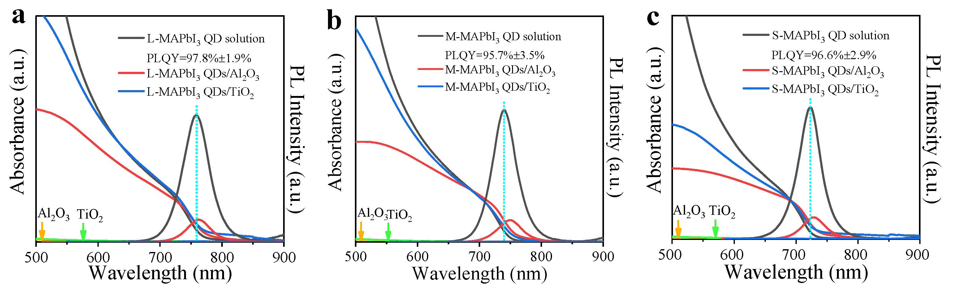
| MAPbI3 QDs | Eg (eV) | λPL (nm) | PLQY (%) |
|---|---|---|---|
| L-QD solution | 1.67 | 758 | 97.8 ± 1.9 |
| M-QD solution | 1.71 | 740 | 95.7 ± 3.5 |
| S-QD solution | 1.75 | 722 | 96.6 ± 2.9 |
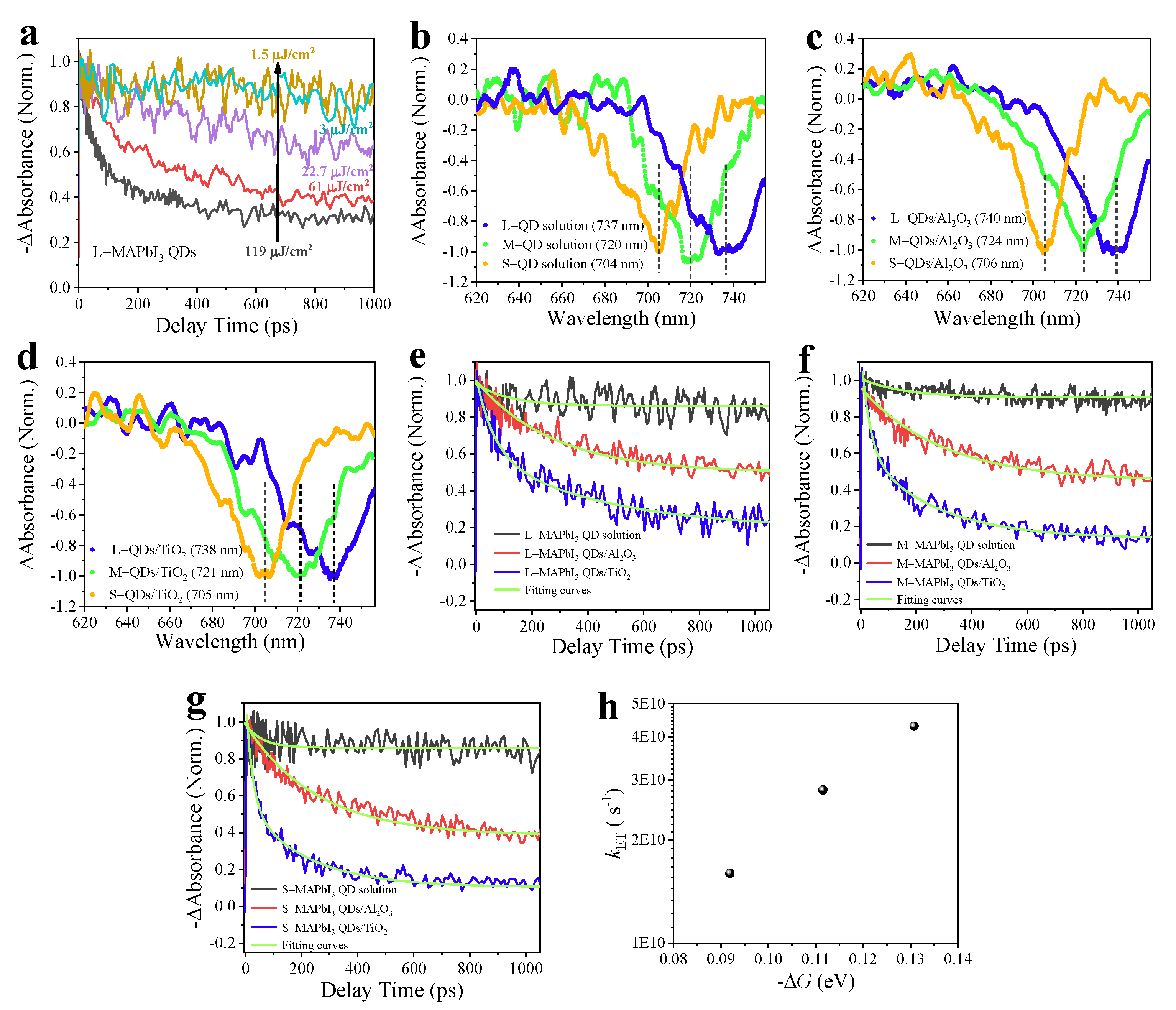
| MAPbI3 QDs | A1 (%) | τ1 (ns) | A2 (%) | τ2 (ns) | τave (ns) |
|---|---|---|---|---|---|
| L-QD solution | 92.0 | 50.8 | 8.0 | 177.0 | 80.1 |
| L-QDs/Al2O3 | 67.2 | 4.2 | 32.8 | 28.7 | 23.0 |
| L-QD/TiO2 | 100 | 2.8 | – | – | 2.8 |
| M-QD solution | 93.5 | 51.9 | 6.5 | 163.3 | 71.9 |
| M-QDs/Al2O3 | 73.7 | 4.0 | 26.3 | 24.9 | 18.4 |
| M-QDs/TiO2 | 100 | 2.4 | – | – | 2.4 |
| S-QD solution | 93.7 | 48.5 | 6.3 | 159.7 | 68.7 |
| S-QDs/Al2O3 | 70.6 | 4.3 | 29.4 | 25.1 | 19.0 |
| S-QDs/TiO2 | 100 | 1.4 | – | – | 1.4 |
| MAPbI3 QDs | A1 | τ1 (ps) | A2 | τ2 (ps) | y0 | kCT (s−1) |
|---|---|---|---|---|---|---|
| L-QD solution | 0.08 | 123 | – | – | 0.92 | – |
| L-QDs/Al2O3 | 0.51 | 278 | – | – | 0.49 | – |
| L-QD/TiO2 | 0.40 | 62 | 0.41 | 331 | 0.19 | 1.6 × 10¹⁰ |
| M-QD solution | 0.09 | 150 | – | – | 0.91 | – |
| M-QDs/Al2O3 | 0.55 | 291 | – | – | 0.45 | – |
| M-QDs/TiO2 | 0.49 | 36 | 0.40 | 287 | 0.11 | 2.8 × 10¹⁰ |
| S-QD solution | 0.09 | 134 | – | – | 0.91 | – |
| S-QDs/Al2O3 | 0.60 | 253 | – | – | 0.40 | – |
| S-QDs/TiO2 | 0.53 | 23 | 0.38 | 215 | 0.09 | 4.3 × 10¹⁰ |
Disclaimer/Publisher’s Note: The statements, opinions and data contained in all publications are solely those of the individual author(s) and contributor(s) and not of MDPI and/or the editor(s). MDPI and/or the editor(s) disclaim responsibility for any injury to people or property resulting from any ideas, methods, instructions or products referred to in the content. |
© 2023 by the authors. Licensee MDPI, Basel, Switzerland. This article is an open access article distributed under the terms and conditions of the Creative Commons Attribution (CC BY) license (https://creativecommons.org/licenses/by/4.0/).
Share and Cite
Li, H.; Ding, C.; Liu, D.; Yajima, S.; Takahashi, K.; Hayase, S.; Shen, Q. Efficient Charge Transfer in MAPbI3 QDs/TiO2 Heterojunctions for High-Performance Solar Cells. Nanomaterials 2023, 13, 1292. https://doi.org/10.3390/nano13071292
Li H, Ding C, Liu D, Yajima S, Takahashi K, Hayase S, Shen Q. Efficient Charge Transfer in MAPbI3 QDs/TiO2 Heterojunctions for High-Performance Solar Cells. Nanomaterials. 2023; 13(7):1292. https://doi.org/10.3390/nano13071292
Chicago/Turabian StyleLi, Hua, Chao Ding, Dong Liu, Shota Yajima, Kei Takahashi, Shuzi Hayase, and Qing Shen. 2023. "Efficient Charge Transfer in MAPbI3 QDs/TiO2 Heterojunctions for High-Performance Solar Cells" Nanomaterials 13, no. 7: 1292. https://doi.org/10.3390/nano13071292