

Structural and Optical Properties of Tungsten Disulfide Nanoscale Films Grown by Sulfurization from W and WO3
 and
and 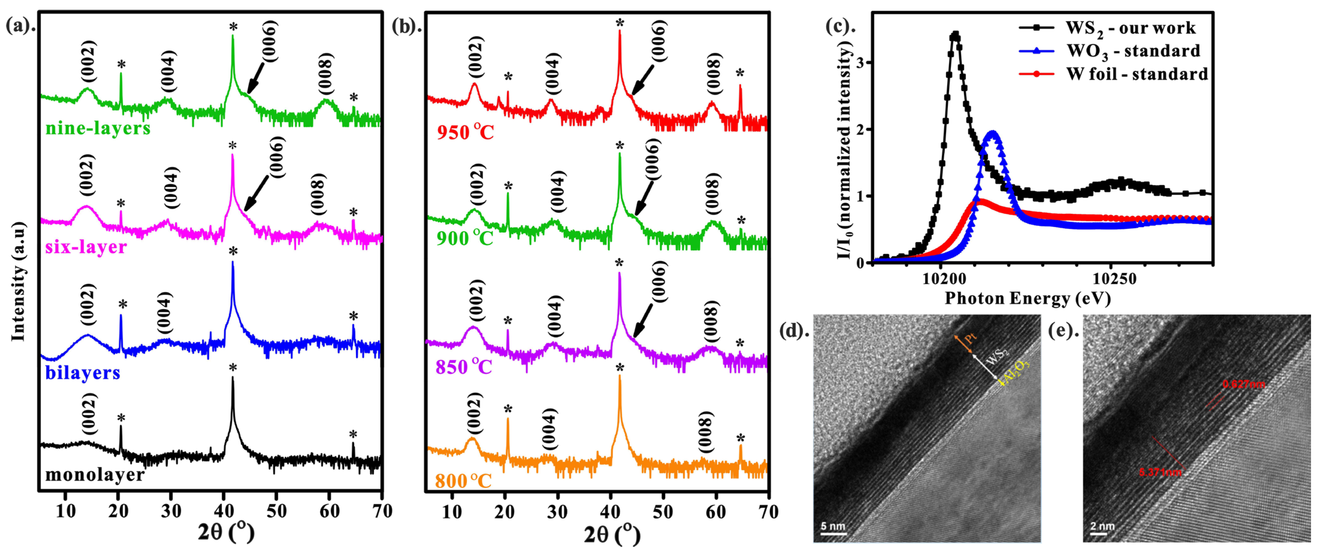
Abstract
:1. Introduction
2. Experimental
3. Results and Discussion
3.1. Structural Analysis
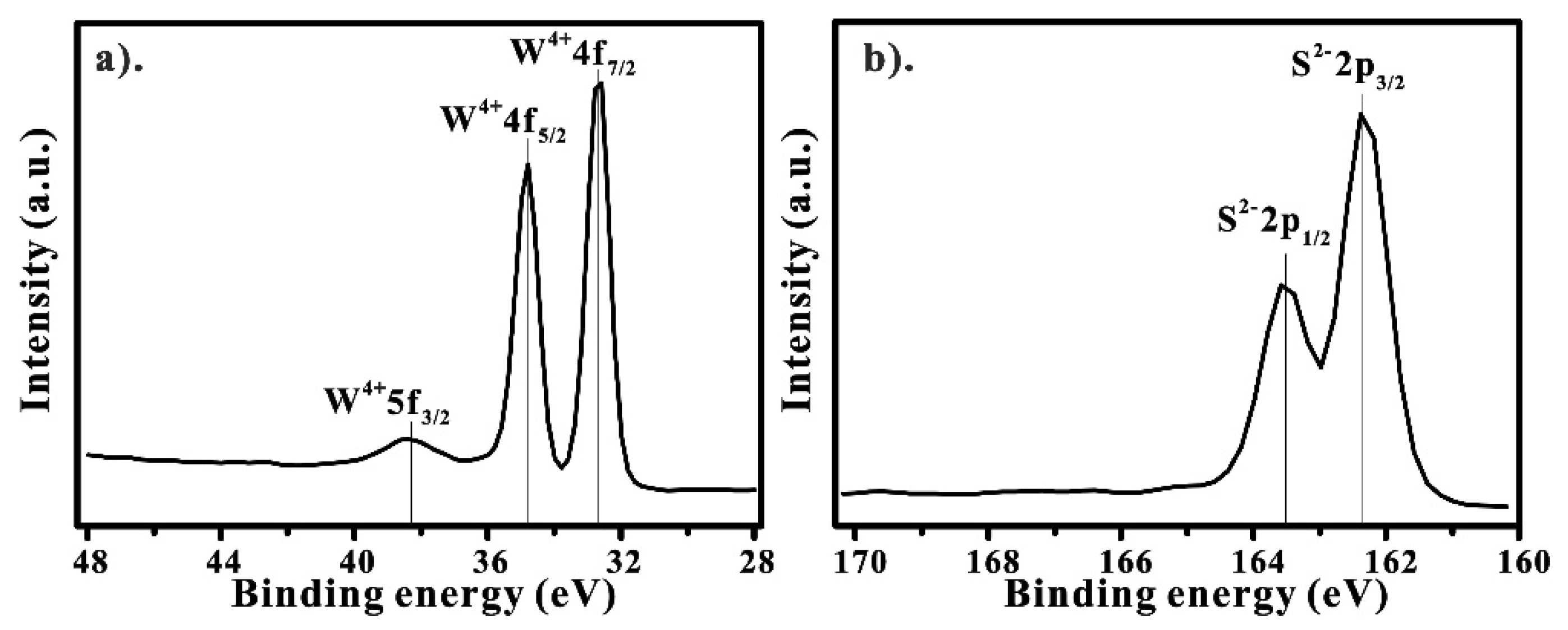
3.2. Elemental Composition Analysis
3.3. Optical Properties
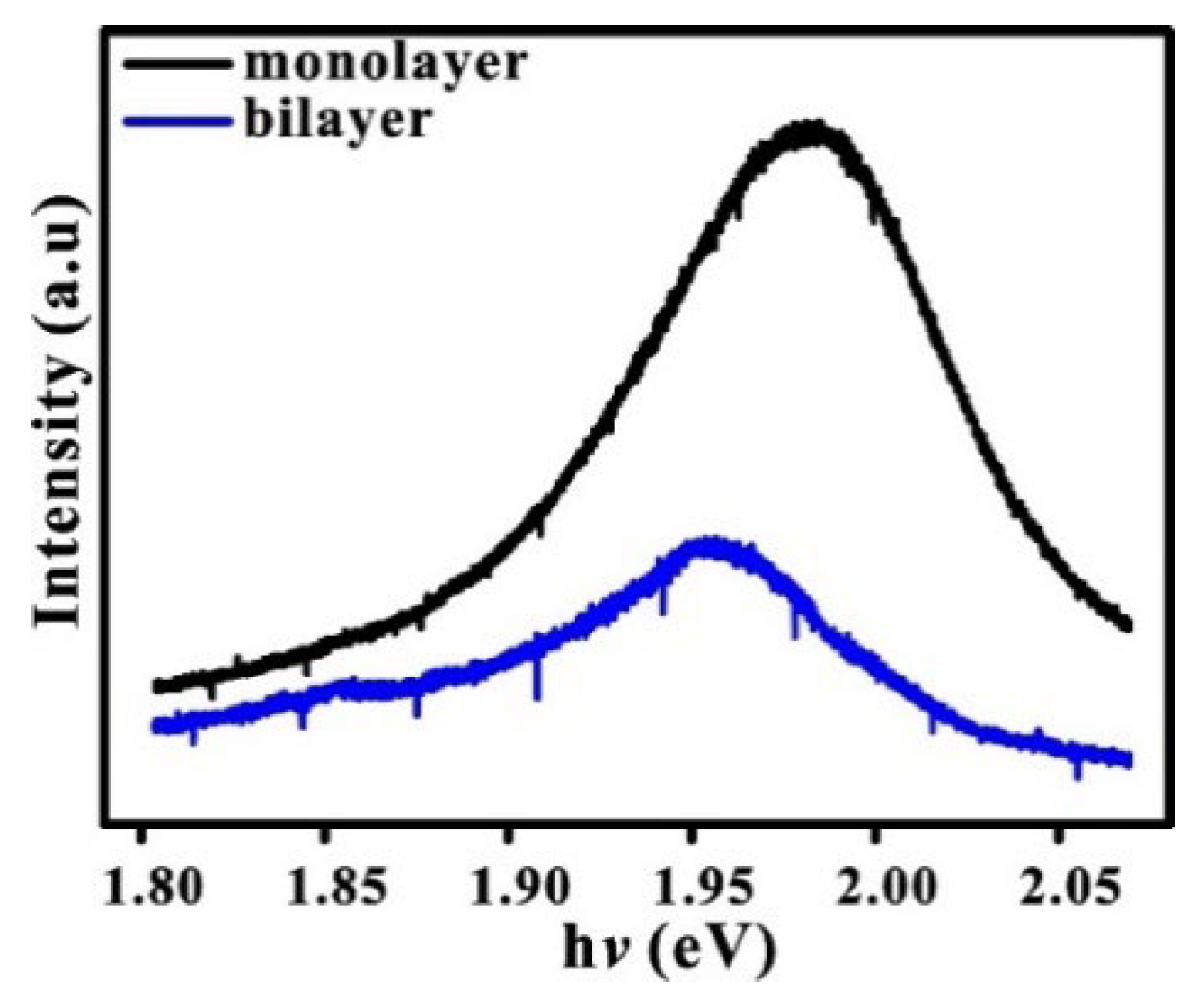
3.3.1. Micro-PL Spectroscopy
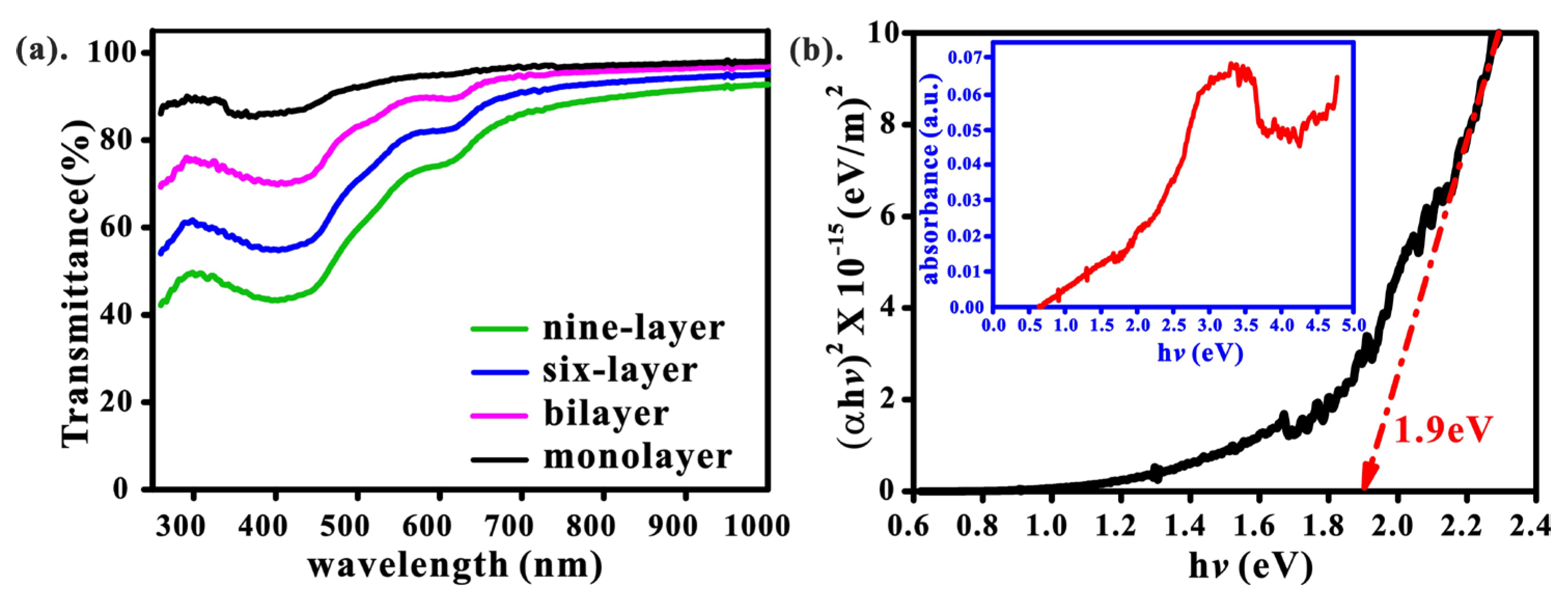
3.3.2. Ultraviolet-Visible-Infrared Spectroscopy
3.4. Comparison of WS2-W and WS2-WO3
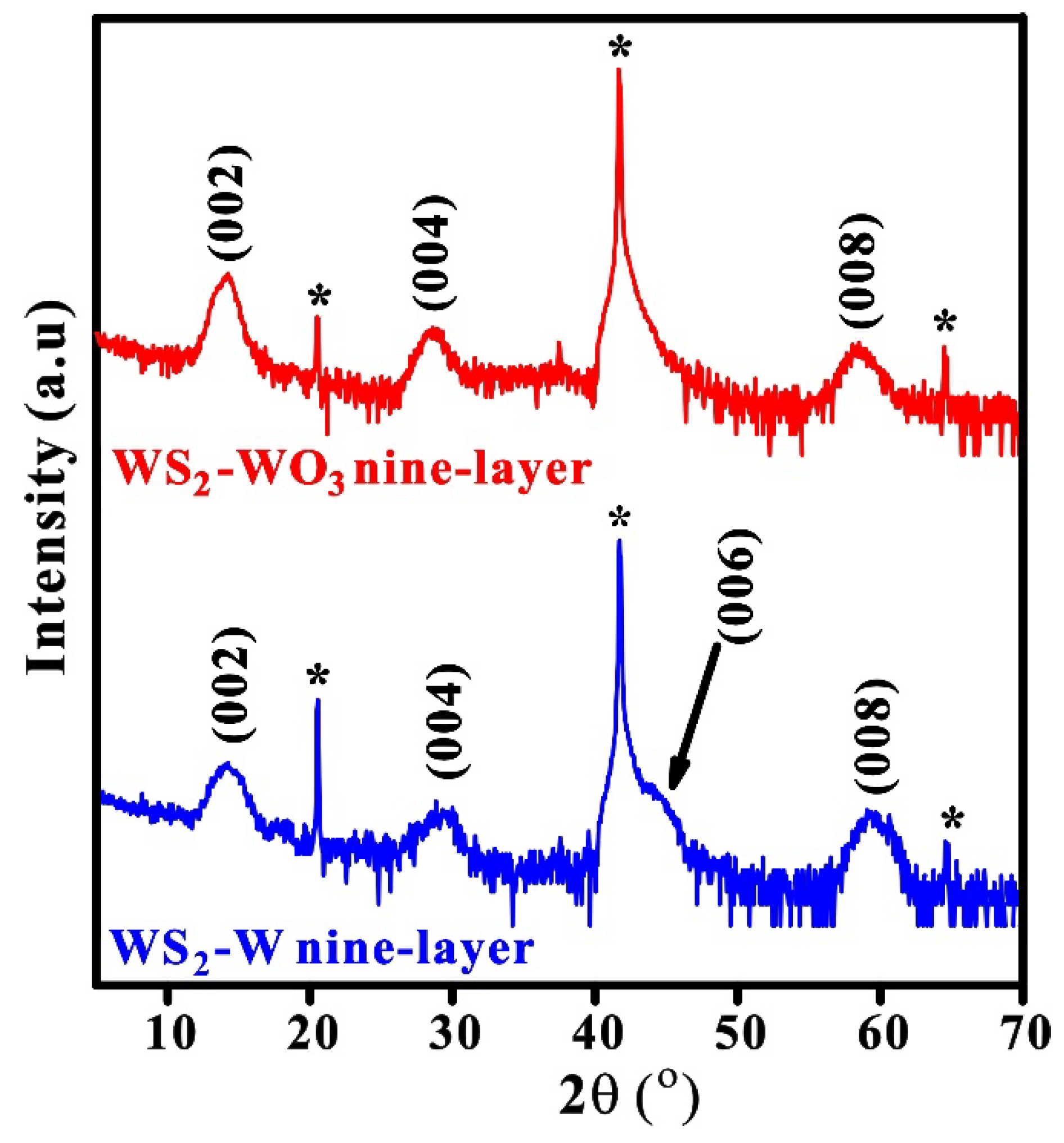
3.4.1. XRD of WS2-W and WS2-WO3
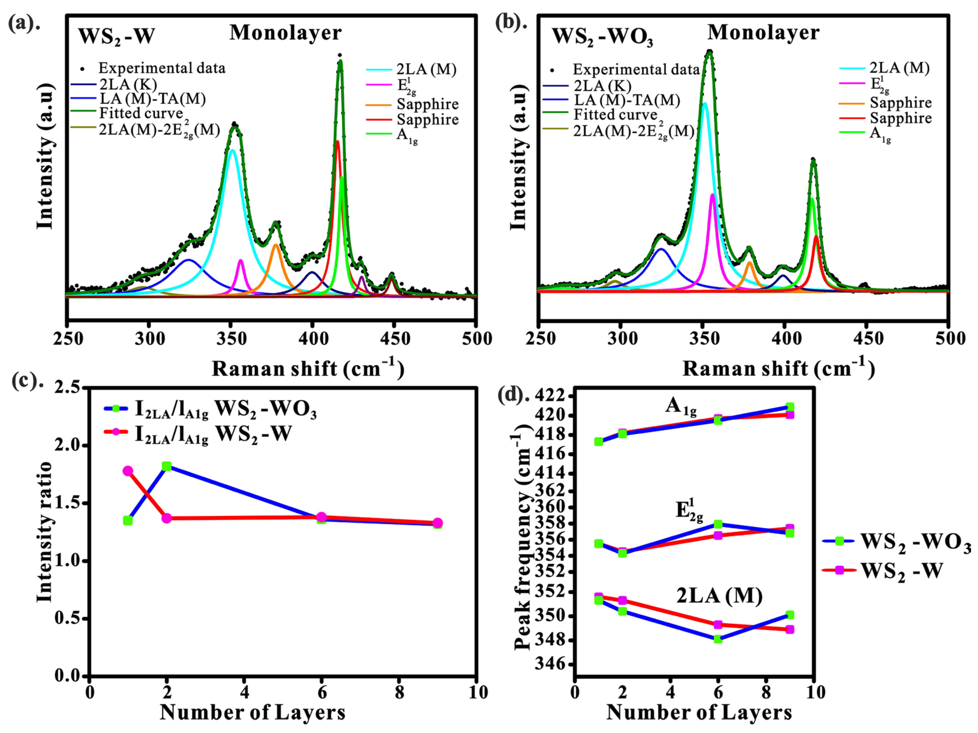
3.4.2. Raman Spectra of WS2-W and WS2-WO3
4. Conclusions
Supplementary Materials
Author Contributions
Funding
Data Availability Statement
Acknowledgments
Conflicts of Interest
References
- Mahler, B.; Hoepfner, V.; Liao, K.; Ozin, G.A. Colloidal synthesis of 1T-WS2 and 2H-WS2 nanosheets: Applications for pho-tocatalytic hydrogen evolution. J. Am. Chem. Soc. 2014, 136, 14121–14127. [Google Scholar] [CrossRef] [PubMed]
- Li, W.; Wang, T.; Dai, X.; Wang, X.; Zhai, C.; Ma, Y.; Chang, S. Bandgap engineering different stacking WS2 bilayer under an external electric field. Solid State Commun. 2016, 225, 32–37. [Google Scholar] [CrossRef]
- Gutierrez, H.R.; Nestor, P.L.; Ana, L.E.; Ayse, B.; Bei, W.; Ruitao, L.; Florentino, L.U.; Vincent, H.C.; Humberto, T.; Mauricio, T. Extraordinary room-temperature photoluminescence in triangular WS2 monolayers. Nano Lett. 2013, 13, 3447–3454. [Google Scholar] [CrossRef] [PubMed] [Green Version]
- Bernardi, M.; Palummo, M.; Grossman, J.C. Extraordinary Sunlight Absorption and One Nanometer Thick Photovoltaics Using Two-Dimensional Monolayer Materials. Nano Lett. 2013, 13, 3664–3670. [Google Scholar] [CrossRef]
- Jo, S.H.; Ubrig, N.; Berger, H.; Kuzmenko, A.B.; Morpurgo, A.F. Mono- and bilayer WS2 light-emitting transistors. Nano Lett. 2014, 14, 2019–2025. [Google Scholar] [CrossRef] [Green Version]
- Liang, L.; Meunier, V. First-principles Raman spectra of MoS2, WS2 and their heterostructures. Nanoscale 2014, 21, 5394–5401. [Google Scholar] [CrossRef]
- Zibouche, N.; Kuc, A.; Heine, T. From layers to nanotubes: Transition metal disulfides TMS2. Eur. Phys. J. B 2012, 85, 49. [Google Scholar] [CrossRef] [Green Version]
- Kuc, A; Zibouche, N; Heine, T. Influence of quantum confinement on the electronic structure of the transition metal sulfide TS2. Phys. Rev. B 2011, 83, 245213. [Google Scholar] [CrossRef] [Green Version]
- Frey, G.L.; Tenne, R.; Matthews, M.J. Optical properties of MS2 (M = Mo, W) inorganic fullerene like and nanotube material optical absorption and resonance Raman measurements. J. Mater. Res. 1998, 13, 9. [Google Scholar] [CrossRef] [Green Version]
- Ghosh, S.; Brüser, V.; Kaplan, A.I.; Popovitz, B.R.; Peglow, S.; Martínez, J.I.; Alonso, J.A.; Zak, A. Cathodoluminescence in single and multiwall WS2 nanotubes: Evidence for quantum confinement and strain effect. Appl. Phys. Rev. 2020, 7, 041401. [Google Scholar] [CrossRef]
- Shanmugam, M.; Durcan, C.A.; Jacobs-Gedrim, R.; Yu, B. Layered semiconductor tungsten disulfide: Photoactive material in bulk heterojunction solar cells. Nano Energy 2013, 2, 419–424. [Google Scholar] [CrossRef]
- Cheng, L.; Huang, W.; Gong, Q.; Liu, C.; Liu, Z.; Li, Y.; Dai, H. Ultrathin WS2 Nanoflakes as a High-Performance Electrocatalyst forth Hydrogen Evolution Reaction. Angew. Chem. Int. Ed 2014, 53, 7860–7863. [Google Scholar] [CrossRef] [PubMed]
- Chen, T.Y.; Chang, Y.H.; Hsu, C.L.; Wei, K.H.; Chiang, C.Y.; Li, L.J. Comparative study on MoS2 and WS2 for electro-catalytic water splitting. Hydrog. Energy Publ. 2013, 38, 12302–12309. [Google Scholar] [CrossRef]
- Feng, C.; Huang, L.; Guo, Z.; Liu, H. Synthesis of tungsten disulfide (WS2) nanoflakes for lithium ion battery application. Electrochem. Commun. 2007, 9, 119. [Google Scholar] [CrossRef]
- Huo, N.; Kang, J.; Wei, Z.; Li, S.S.; Li, J.; Wei, S.H. Novel and Enhanced Optoelectronic Performances of Multilayer MoS 2 –WS 2 Heterostructure Transistors. Adv. Funct. Mater 2014, 24, 7025–7031. [Google Scholar] [CrossRef]
- Elías, A.L.; Perea-López, N.; Castro-Beltrán, A.; Berkdemir, A.; Lv, R.; Feng, S.; Long, A.D.; Hayashi, T.; Kim, Y.A.; Endo, M.; et al. Controlled synthesis and transfer of large-area WS2 sheets: From single layer to few layers. ACS Nano 2013, 7, 5235–5242. [Google Scholar] [CrossRef]
- Miremadi, B.K.; Morrison, S.R. The intercalation and exfoliation of tungsten disulfide. J. Appl. Phys. 1988, 63, 4970–4974. [Google Scholar] [CrossRef]
- Cong, C.; Shang, J.; Wu, X.; Cao, B.; Peimyoo, N.; Qiu, C.; Sun, L.; Yu, T. Synthesis and optical properties of large-area sin-gle-crystalline 2D semiconductor WS2monolayer from chemical vapor deposition. Adv. Opt. Mater 2013, 2, 131–136. [Google Scholar] [CrossRef]
- Modtland, B.J.; Efren, N.M.; Xiang, J.; Marc, B.; Jing, K. Monolayer tungsten disulfide (WS2) via chlorine-driven chemical vapor transport. Small 2017, 1701232. [Google Scholar] [CrossRef]
- Wan, L.; Shi, C.W.; Yu, Z.B.; Wu, H.D.; Xiao, W.; Geng, Z.X.; Ren, T.Q.; Han, Q.; Yang, Z.X. Preparation of WS2/C composite material and its electrocatalytic hydrogen evolution performance. J. Fuel Chem. Technol. 2021, 49, 1362–1370. [Google Scholar] [CrossRef]
- Ramakrishna Matte, H.S.S.; Gomathi, A.; Manna, A.K.; Late, D.J.; Datta, R.; Pati, S.K.; Rao, C.N.R. MoS2 and WS2 Analogues of graphene. Angew. Chem. Int. Ed 2010, 49, 4059–4062. [Google Scholar] [CrossRef] [PubMed]
- Schutte, W.J.; Deboer, J.L.; Jellinek, F. Crystal-Structures of Tungsten Disulfide and Diselenide. J. Solid State Chem. 1987, 70, 207–209. [Google Scholar] [CrossRef]
- Prouzet, E.; Heising, J.; Kanatzidis, M.G. Structure of Restacked and Pillared WS2: An X-ray Absorption Study. Chem. Mater. 2003, 15, 412–418. [Google Scholar] [CrossRef]
- Wang, J.; Yu, L.; Zhou, Z.; Zeng, L.; Wei, M. Template-free synthesis of metallic WS2 hollow microspheres as an anode for the sodium-ion battery. J. Colloid Interface Sci. 2013, 557, 722–728. [Google Scholar] [CrossRef] [PubMed]
- Cao, H.; Wen, F.; De Hosson, J.T.M.; Pei, Y.T. Instant WS2 platelets reorientation of self-adaptive WS2/a-C tribocoating. Mater. Lett. 2018, 229, 64–67. [Google Scholar] [CrossRef]
- Yang, W.; Wang, J.; Si, C.; Peng, Z.; Frenzel, J.; Eggeler, G.; Zhang, Z. [001] Preferentially-oriented 2D tungsten disulfide nanosheets as anode materials for superior lithium storage. J. Mater. Chem A 2015, 3, 17811. [Google Scholar] [CrossRef]
- Xu, S.; Gao, X.; Hu, M.; Sun, J.; Wang, D.; Zhou, F.; Weng, L.; Liu, W. Morphology Evolution of Ag Alloyed WS2 Films and the Significantly Enhanced Mechanical and Tribological Properties. Surf. Coat. Technol. 2014, 238, 197–206. [Google Scholar] [CrossRef]
- Frey, G.L.; Elani, S.; Homyonfer, M.; Feldman, Y.; Tenne, R. Optical-absorption spectra of inorganic fullerene like MS2 (M = Mo, W). Phys. Rev. B 1998, 57, 6666–6671. [Google Scholar] [CrossRef]
- Beal, A.R.; Liang, W.Y. Excitons in 2H-WSe2 and 3R-WS2. J. Phys. C Solid State Phys. 1976, 9, 2459–2466. [Google Scholar] [CrossRef]
- Berkdemir, A.; Gutiérrez, H.R.; Botello-Méndez, A.R.; Perea-López, N.; Elías, A.L.; Chia, C.I.; Wang, B.; Crespi, V.H.; López-Urías, F.; Charlier, J.C.; et al. Identification of individual and few layers of WS2 using Raman Spectroscopy. Sci. Rep. 2013, 3, 1755. [Google Scholar] [CrossRef] [Green Version]
- Zhao, W.; Ghorannevis, Z.; Amara, K.K.; Pang, J.R.; Toh, M.; Zhang, X.; Kloc, C.; Tan, P.H.; Eda, G. Lattice dynamics in mono- and few-layer sheets of WS2 and WSe2. Nanoscale 2013, 5, 9677. [Google Scholar] [CrossRef] [Green Version]
- Tongay, S.; Zhou, J.; Ataca, C.; Lo, K.; Matthews, T.S.; Li, J.; Grossman, J.C.; Wu, J. Thermally Driven Crossover from Indirect toward Direct Bandgap in 2D Semiconductors: MoSe2 versus MoS2. Nano Lett. 2012, 12, 5576–5580. [Google Scholar] [CrossRef] [PubMed]
- Lui, C.H.; Li, Z.; Chen, Z.; Klimov, P.V.; Brus, L.E.; Heinz, T.F. Imaging stacking order in few-layer graphene. Nano Lett. 2011, 11, 164–169. [Google Scholar] [CrossRef] [PubMed] [Green Version]
- Stacy, A.M.; Hodul, D.T. Raman-Spectra of Ivb and Vib Transition-Metal Disulfides Using Laser Energies near the Absorption Edges. J. Phys. Chem. Solids 1985, 46, 405–409. [Google Scholar] [CrossRef]
- Molina-Sanchez, A.; Wirtz, L. Phonons in single-layer and few-layer MoS2 and WS2. Phys. Rev. B 2011, 84, 155413. [Google Scholar] [CrossRef] [Green Version]
- Zhang, Y.; Zhang, Y.; Ji, Q.; Ju, J.; Yuan, H.; Shi, J.; Gao, T.; Ma, D.; Liu, M.; Chen, Y.; et al. Controlled Growth of High-Quality Monolayer WS2 Layers on Sapphire and Imaging Its Grain Boundary. ACS Nano 2013, 7, 8963–8971. [Google Scholar] [CrossRef] [PubMed]
- Huang, X.; Gao, Y.; Yang, T.; Ren, W.; Cheng, H.M.; Lai, T. Quantitative Analysis of Temperature Dependence of Raman shift of monolayer WS2. Sci. Rep. 2016, 6, 32236. [Google Scholar] [CrossRef] [PubMed] [Green Version]
- Song, J.G.; Park, J.; Lee, W.; Choi, T.; Jung, H.; Lee, C.W.; Hwang, S.H.; Myoung, J.M.; Jung, J.H.; Kim, S.H.; et al. Layer-Controlled, Wafer-Scale, and Conformal Synthesis of Tungsten Disulfide Nanosheets Using Atomic Layer Deposition. ACS Nano 2013, 7, 11333–11340. [Google Scholar] [CrossRef]
- Sekine, T.; Nakashizu, T.; Toyoda, K.; Uchinokura, K.; Matsuura, E. Raman scattering in layered compound 2H-WS2. Solid State Commun. 1980, 35, 371–373. [Google Scholar] [CrossRef]
- Sie, E.J.; Steinhoff, A.; Gies, C.; Lui, C.H.; Ma, Q.; Rosner, M.; Schönhoff, G.; Jahnke, F.; Wehling, T.O.; Lee, Y.H.; et al. Observation of exciton redshift–blueshift crossover in monolayer WS2. Nano Lett. 2017, 14, 4210–4216. [Google Scholar] [CrossRef] [Green Version]
- Cao, S.; Zhao, C.; Han, T.; Peng, L. The WO3/WS2 nanostructures: Preparation, characterization and optical absorption properties. Physical E 2016, 81, 235–239. [Google Scholar] [CrossRef]
- Sun, Y.; Darling, A.J.; Li, Y.; Fujisawa, K.; Holder, C.F.; Liu, H.; Janik, M.J.; Terrones, M.; Schaak, R.E. De-fect-mediated selective hydrogenation of nitroarenes on nanostructured WS2. Chem. Sci. 2019, 10, 10310. [Google Scholar] [CrossRef] [PubMed] [Green Version]


Disclaimer/Publisher’s Note: The statements, opinions and data contained in all publications are solely those of the individual author(s) and contributor(s) and not of MDPI and/or the editor(s). MDPI and/or the editor(s) disclaim responsibility for any injury to people or property resulting from any ideas, methods, instructions or products referred to in the content. |
© 2023 by the authors. Licensee MDPI, Basel, Switzerland. This article is an open access article distributed under the terms and conditions of the Creative Commons Attribution (CC BY) license (https://creativecommons.org/licenses/by/4.0/).
Share and Cite
Gultom, P.; Chiang, J.-Y.; Huang, T.-T.; Lee, J.-C.; Su, S.-H.; Huang, J.-C.A. Structural and Optical Properties of Tungsten Disulfide Nanoscale Films Grown by Sulfurization from W and WO3. Nanomaterials 2023, 13, 1276. https://doi.org/10.3390/nano13071276
Gultom P, Chiang J-Y, Huang T-T, Lee J-C, Su S-H, Huang J-CA. Structural and Optical Properties of Tungsten Disulfide Nanoscale Films Grown by Sulfurization from W and WO3. Nanomaterials. 2023; 13(7):1276. https://doi.org/10.3390/nano13071276
Chicago/Turabian StyleGultom, Pangihutan, Jiang-Yan Chiang, Tzu-Tai Huang, Jung-Chuan Lee, Shu-Hsuan Su, and Jung-Chung Andrew Huang. 2023. "Structural and Optical Properties of Tungsten Disulfide Nanoscale Films Grown by Sulfurization from W and WO3" Nanomaterials 13, no. 7: 1276. https://doi.org/10.3390/nano13071276