
Nanocomposites of Silicon Oxides and Carbon: Its Study as Luminescent Nanomaterials
 , , , , , ,
Abstract
:
1. Introduction
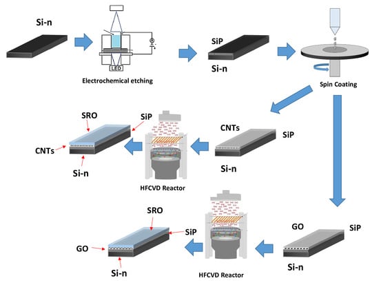
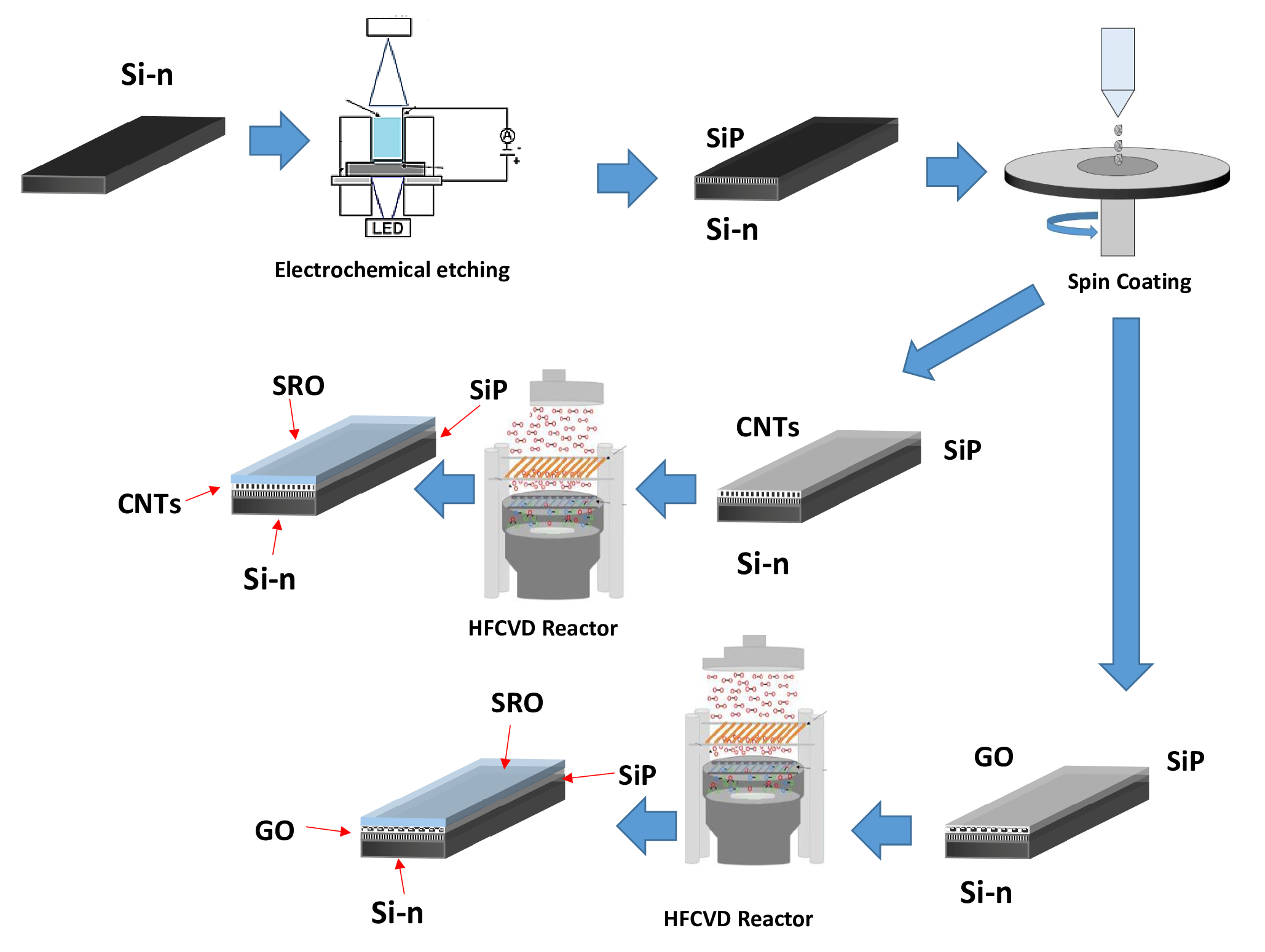
2. Materials and Methods
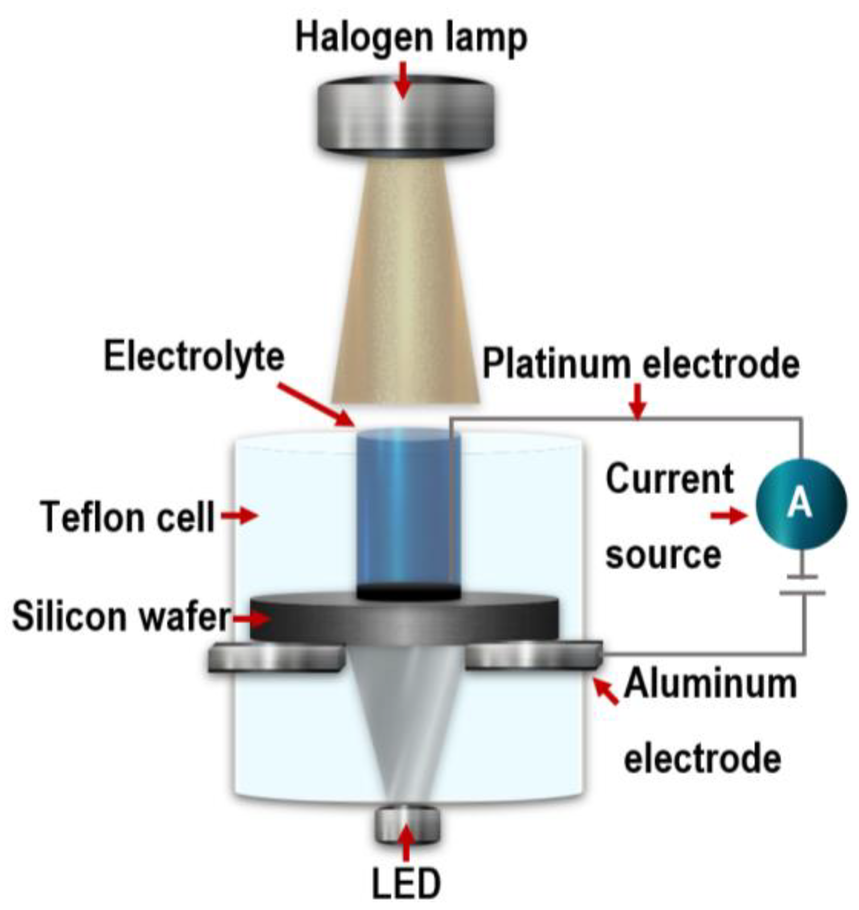
3. Results and Discussion
4. Conclusions
Author Contributions
Funding
Data Availability Statement
Acknowledgments
Conflicts of Interest
References
- Canham, L.T. Silicon Quantum Wire Array Fabrication by Electrochemical and Chemical Dissolution of Wafers. Appl. Phys. Lett. 1990, 57, 1046–1048. [Google Scholar] [CrossRef]
- Hlinomaz, P.; Klíma, O.; Hospodková, A.; Hulicius, E.; Oswald, J.; Šípek, E.; Kočka, J. Photoelectric Properties of Self-Supporting Porous Silicon. Appl. Phys. Lett. 1994, 64, 3118–3120. [Google Scholar] [CrossRef]
- Dzhafarov, T. Silicon solar cells with nanoporous silicon layer. Sol. Cells—Res. Appl. Perspect. 2013, 1, 42. [Google Scholar] [CrossRef] [Green Version]
- Gelloz, B.; Juangsa, F.B.; Nozaki, T.; Asaka, K.; Koshida, N.; Jin, L. Si/SiO2 Core/Shell Luminescent Silicon Nanocrystals and Porous Silicon Powders with High Quantum Yield, Long Lifetime, and Good Stability. Front. Phys. 2019, 7, 47. [Google Scholar] [CrossRef] [Green Version]
- Kazanskiy, N.L.; Khonina, S.N.; Butt, M.A. Advancement in silicon integrated photonics technologies for sensing applications in near-infrared and Mid-Infrared Region: A Review. Photonics 2022, 9, 331. [Google Scholar] [CrossRef]
- Cheong, I.T.; Mock, J.; Kallergi, M.; Groß, E.; Meldrum, A.; Rieger, B.; Becherer, M.; Veinot, J.G. Colloidal Silicon Quantum Dot-Based Cavity Light-Emitting Diodes with Narrowed and Tunable Electroluminescence. Adv. Opt. Mater. 2022, 11, 2201834. [Google Scholar] [CrossRef]
- Hernández Simón, Z.J.; Luna López, J.A.; Hernández de la Luz, Á.D.; Garcia Salgado, G.; Monfil Leyva, K.; Carrillo López, J.; Mendoza Conde, G.O.; Benítez Lara, A.; Martínez Hernández, H.P.; Gastellou Hernández, E.; et al. SiOx Films Deposited by HFCVD: Their Conduction Response to Light and Intrinsic Photovoltaic Effect. Surf. Interfaces 2021, 26, 101411. [Google Scholar] [CrossRef]
- Martínez Hernández, H.P.; Luna López, J.A.; Morales, R.; Casco, J.F.; Hernández de la Luz, J.A.; Luna, A.; Hernández Simón, Z.J.; Mendoza Conde, G.O.; Monfil Leyva, K.; Ramírez Amador, R.; et al. Blue Electroluminescence in SRO-HFCVD Films. Nanomaterials 2021, 11, 943. [Google Scholar] [CrossRef]
- Hernández Simón, Z.J.; Luna López, J.A.; de la Luz, A.D.; Pérez García, S.A.; Benítez Lara, A.; García Salgado, G.; Carrillo López, J.; Mendoza Conde, G.O.; Martínez Hernández, H.P. Spectroscopic Properties of Si-NC in SiOx Films Using HFCVD. Nanomaterials 2020, 10, 1415. [Google Scholar] [CrossRef]
- Martínez Hernández, H.P.; Luna López, J.A.; Hernández de la Luz, J.A.; Luna Flores, A.; Monfil Leyva, K.; García Salgado, G.; Carrillo López, J.; Ordoñez Flores, R.; Pérez García, S.; Hernández Simón, Z.J.; et al. Spectroscopic and Microscopic Correlation of SRO-HFCVD Films on Quartz and Silicon. Crystals 2020, 10, 127. [Google Scholar] [CrossRef] [Green Version]
- Avouris, P.; Freitag, M.; Perebeinos, V. Carbon-Nanotube Photonics and Optoelectronics. Nat. Photonics 2008, 2, 341–350. [Google Scholar] [CrossRef]
- Cayuela, A.; Soriano, M.L.; Valcárcel, M. Photoluminescent Carbon Dot Sensor for Carboxylated Multiwalled Carbon Nanotube Detection in River Water. Sens. Actuators B Chem. 2015, 207, 596–601. [Google Scholar] [CrossRef]
- Ebrahimi Naghani, M.; Neghabi, M.; Zadsar, M.; Abbastabar Ahangar, H. Synthesis and characterization of linear/nonlinear optical properties of graphene oxide and reduced graphene oxide-based zinc oxide nanocomposite. Sci. Rep. 2023, 13, 1496. [Google Scholar] [CrossRef] [PubMed]
- Montes-Navajas, P.; Asenjo, N.G.; Santamaría, R.; Menéndez, R.; Corma, A.; García, H. Surface Area Measurement of Graphene Oxide in Aqueous Solutions. Langmuir 2013, 29, 13443–13448. [Google Scholar] [CrossRef] [PubMed]
- Han, J.T.; Kim, J.S.; Jo, S.B.; Kim, S.H.; Kim, J.S.; Kang, B.; Jeong, H.J.; Jeong, S.Y.; Lee, G.-W.; Cho, K. Graphene Oxide as a Multi-Functional p-Dopant of Transparent Single-Walled Carbon Nanotube Films for Optoelectronic Devices. Nanoscale 2012, 4, 7735. [Google Scholar] [CrossRef] [PubMed]
- Jin, Y.; Zheng, Y.; Podkolzin, S.G.; Lee, W. Band Gap of Reduced Graphene Oxide Tuned by Controlling Functional Groups. J. Mater. Chem. C 2020, 8, 4885–4894. [Google Scholar] [CrossRef]
- Ruzyllo, J.; Hattori, T.; Novak, R. Cleaning Technology in Semiconductor Device Manufacturing VIII: Proceedings of the International Symposium; Electrochemical Society: Pennington, NJ, USA, 2004. [Google Scholar]
- Victoriano Huerta, N.; Luna López, J.A.; Hernández de la Luz, J.A.D.; Gómez Barojas, E.; Benitez Lara, A.; Monfil Leyva, K.; Domínguez Jimenez, M.A. Optical, Morphological and Electrical Analysis of Heterostructures PSI/C-Si and SIO2/Mwcnts/PSI/C-Si. Sens. Actuators A Phys. 2018, 282, 55–62. [Google Scholar] [CrossRef]
- Wang, W.; Ruderer, M.A.; Metwalli, E.; Guo, S.; Herzig, E.M.; Perlich, J.; Müller-Buschbaum, P. Effect of Methanol Addition on the Resistivity and Morphology of PEDOT: PSS Layers on Top of Carbon Nanotubes for Use as Flexible Electrodes. ACS Appl. Mater. Interfaces 2015, 7, 8789–8797. [Google Scholar] [CrossRef]
- Lai, C.; Li, X.; Liu, C.; Guo, X.; Xiang, Z.; Xie, B.; Zou, L. Improvement in Gravimetric Measurement for Determining the Porosity and Thickness of Porous Silicon Using an Optimized Solution. Mater. Sci. Semicond. Process. 2014, 26, 501–505. [Google Scholar] [CrossRef]
- Khardani, M.; Bouaïcha, M.; Bessaïs, B. Bruggeman effective medium approach for modelling optical properties of porous silicon: Comparison with experiment. Phys. Status Solidi C 2007, 4, 1986–1990. [Google Scholar] [CrossRef]
- Sohn, H. Refractive index of porous silicon. Handb. Porous Silicon 2018, 1, 341–352. [Google Scholar] [CrossRef]
- Park, S.J.; Ok, J.G.; Park, H.J.; Lee, K.-T.; Lee, J.H.; Kim, J.D.; Cho, E.; Baac, H.W.; Kang, S.; Guo, L.J.; et al. Modulation of the effective density and refractive index of carbon nanotube forests via Nanoimprint Lithography. Carbon 2018, 129, 8–14. [Google Scholar] [CrossRef]
- Wang, X.; Chen, Y.P.; Nolte, D.D. Strong anomalous optical dispersion of graphene: Complex refractive index measured by Picometrology. Opt. Express 2008, 16, 22105. [Google Scholar] [CrossRef] [PubMed]
- Chan, K.S.; Dwight, T.J. Photoluminescence, Morphological and Electrical Properties of Porous Silicon Formulated with Different HNO3 Concentrations. Results Phys. 2018, 10, 5–9. [Google Scholar] [CrossRef]
- Al-Douri, Y.; Badi, N.; Voon, C.H. Etching Time Effect on Optical Properties of Porous Silicon for Solar Cells Fabrication. Optik 2017, 147, 343–349. [Google Scholar] [CrossRef]
- Cullis, A.G.; Canham, L.T. Visible Light Emission Due to Quantum Size Effects in Highly Porous Crystalline Silicon. Nature 1991, 353, 335–338. [Google Scholar] [CrossRef]
- Omar, K.; Al-Douri, Y.; Ramizy, A.; Hassan, Z. Stiffness Properties of Porous Silicon Nanowires Fabricated by Electrochemical and Laser-Induced Etching. Superlattices Microstruct. 2011, 50, 119–127. [Google Scholar] [CrossRef]
- Amdouni, S.; Rahmani, M.; Zaïbi, M.-A.; Oueslati, M. Enhancement of Porous Silicon Photoluminescence by Electroless Deposition of Nickel. J. Lumin. 2015, 157, 93–97. [Google Scholar] [CrossRef]
- Lin, L.; Li, D.X.; Feng, J. First-Principles Study of the Band Gap Structure of Oxygen-Passivated Silicon Nanonets. Nanoscale Res. Lett. 2009, 4, 409–413. [Google Scholar] [CrossRef] [Green Version]
- Bisi, O.; Ossicini, S.; Pavesi, L. Porous Silicon: A Quantum Sponge Structure for Silicon Based Optoelectronics. Surf. Sci. Rep. 2000, 38, 1–126. [Google Scholar] [CrossRef]
- Cullis, A.G.; Canham, L.T.; Calcott, P.D. The Structural and Luminescence Properties of Porous Silicon. J. Appl. Phys. 1997, 82, 909–965. [Google Scholar] [CrossRef]
- Mulloni, V.; Pavesi, L. Electrochemically Oxidised Porous Silicon Microcavities. Mater. Sci. Eng. B 2000, 69–70, 59–65. [Google Scholar] [CrossRef]
- Elhouichet, H.; Oueslati, M. The Role of Ambient Ageing on Porous Silicon Photoluminescence: Evidence of Phonon Contribution. Appl. Surf. Sci. 2002, 191, 11–19. [Google Scholar] [CrossRef]
- Wang, Y.; Townsend, P.D. Common Mistakes in Luminescence Analysis. J. Phys. Conf. Ser. 2012, 398, 012003. [Google Scholar] [CrossRef] [Green Version]
- De Boer, W.D.; Timmerman, D.; Dohnalová, K.; Yassievich, I.N.; Zhang, H.; Buma, W.J.; Gregorkiewicz, T. Red Spectral Shift and Enhanced Quantum Efficiency in Phonon-Free Photoluminescence from Silicon Nanocrystals. Nat. Nanotechnol. 2010, 5, 878–884. [Google Scholar] [CrossRef]
- Karacali, T.; Cakmak, B.; Efeoglu, H. Aging of porous silicon and the origin of blue shift. Opt. Express 2003, 11, 1237. [Google Scholar] [CrossRef]
- Chen, J.; Li, D.; Sun, T.; Han, J.; Wang, L.; Zhang, Y.; Xu, J.; Chen, K. Study on Luminescence Quenching of Ultra-Small Silicon Nanocrystals Due to Boron Doping. Opt. Mater. Express 2022, 12, 4096. [Google Scholar] [CrossRef]
- Águila Rodríguez, G.; García-Salgado, G.; Romero-Paredes, G.; Peña-Sierra, R. FTIR and photoluminescence studies of porous silicon layers oxidized in controlled water vapor conditions. Rev. Mex. De Física 2007, 53, 431–435. [Google Scholar]
- Fedoseeva, Y.V.; Bulusheva, L.G.; Okotrub, A.V.; Kanygin, M.A.; Gorodetskiy, D.V.; Asanov, I.P.; Vyalikh, D.V.; Puzyr, A.P.; Bondar, V.S. Field Emission Luminescence of Nanodiamonds Deposited on the Aligned Carbon Nanotube Array. Sci. Rep. 2015, 5, 9379. [Google Scholar] [CrossRef] [Green Version]
- Du, D.; Song, H.; Nie, Y.; Sun, X.; Chen, L.; Ouyang, J. Photoluminescence of Graphene Oxide in Visible Range Arising from Excimer Formation. J. Phys. Chem. C 2015, 119, 20085–20090. [Google Scholar] [CrossRef]
- Zhou, J.; Zhou, X.; Li, R.; Sun, X.; Ding, Z.; Cutler, J.; Sham, T. Electronic structure and luminescence center of blue luminescent carbon nanocrystals. Chem. Phys. Lett. 2009, 474, 320–324. [Google Scholar] [CrossRef]
- Vaccaro, L.; Cannas, M.; Radzig, V. Luminescence properties of nonbridging oxygen hole centers at the silica surface. J. Non-Cryst. Solids 2009, 355, 1020–1023. [Google Scholar] [CrossRef]
- Liu, F.; Cao, Y.; Yi, M.; Xie, L.; Huang, W.; Tang, N.; Zhong, W.; Du, Y. Thermostability, Photoluminescence, and Electrical Properties of Reduced Graphene Oxide–Carbon Nanotube Hybrid Materials. Crystals 2013, 3, 28–37. [Google Scholar] [CrossRef] [Green Version]
- Victoria, A.P.; de la Luz, A.D.; Juárez, J.M.; Espinosa-Torres, N.D.; Robles-Águila, M.J.; López, J.A.; Juárez-Díaz, G. Photoluminescence Spectrum Using DFT for Double-Walled Carbon Nanotubes with Metallic Constituents. J. Mol. Model. 2019, 25, 1–8. [Google Scholar] [CrossRef] [PubMed]
- Santiago, S.R.; Chang, C.-H.; Lin, T.-N.; Yuan, C.-T.; Shen, J.-L. Diethylenetriamine-doped graphene oxide quantum dots with tunable photoluminescence for optoelectronic applications. ACS Appl. Nano Mater. 2019, 2, 3925–3933. [Google Scholar] [CrossRef]
- Sun, J.; Yang, S.; Wang, Z.; Shen, H.; Xu, T.; Sun, L.; Li, H.; Chen, W.; Jiang, X.; Ding, G.; et al. Ultra-high quantum yield of graphene quantum dots: Aromatic-nitrogen doping and photoluminescence mechanism. Part. Part. Syst. Charact. 2014, 32, 434–440. [Google Scholar] [CrossRef]
- Chien, C.T.; Li, S.S.; Lai, W.J.; Yeh, Y.C.; Chen, H.A.; Chen, I.S.; Chen, L.C.; Chen, K.H.; Nemoto, T.; Isoda, S.; et al. Tunable photoluminescence from graphene oxide. Angew. Chem. Int. Ed. 2012, 51, 6662–6666. [Google Scholar] [CrossRef]
- Mei, Q.; Liu, B.; Han, G.; Liu, R.; Han, M.Y.; Zhang, Z. Graphene oxide: From tunable structures to diverse luminescence behaviors. Adv. Sci. 2019, 6, 1900855. [Google Scholar] [CrossRef] [Green Version]


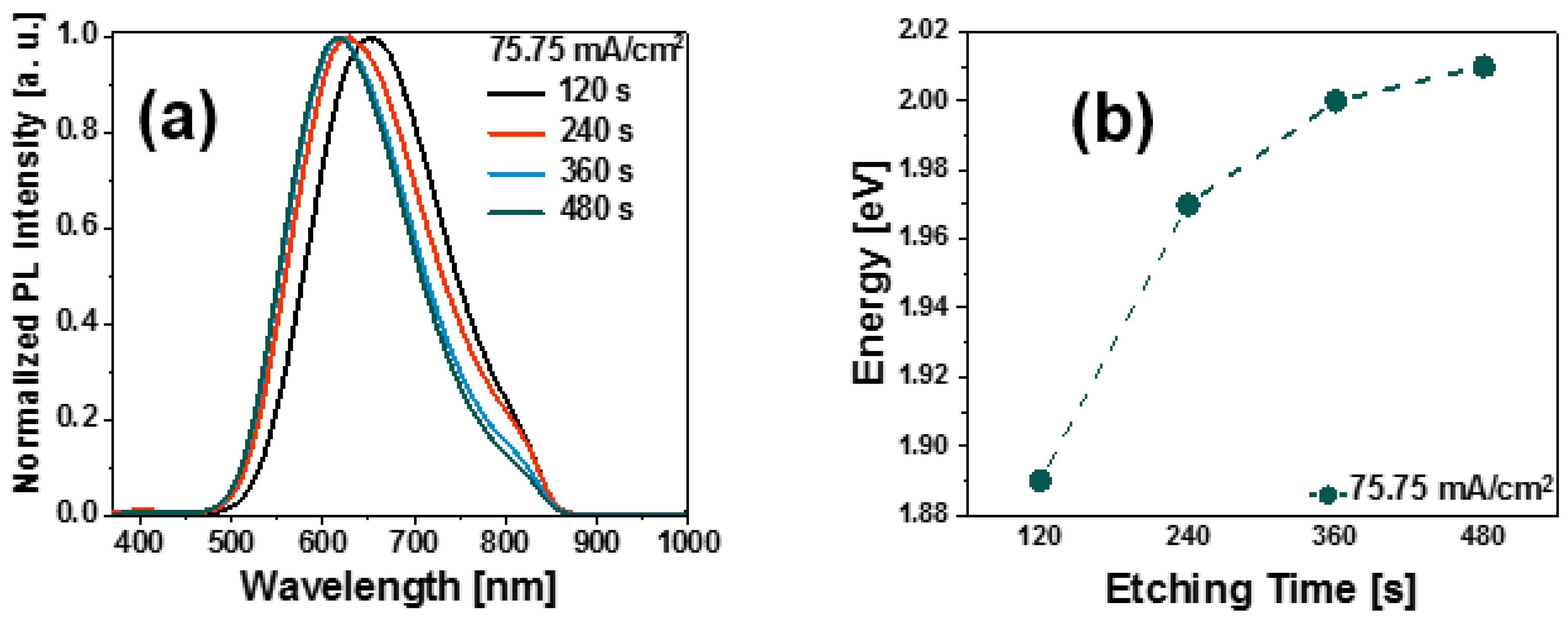
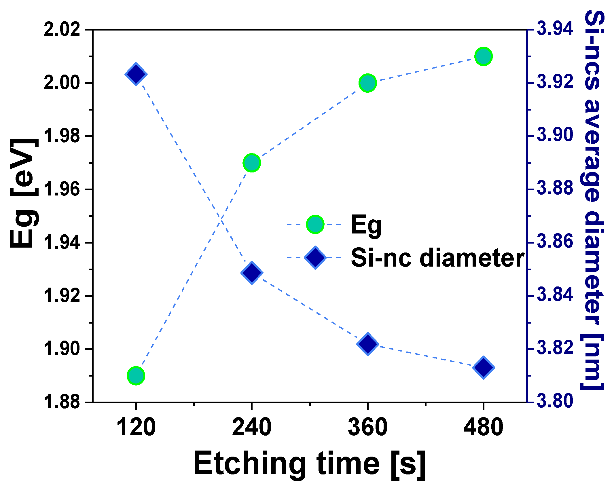
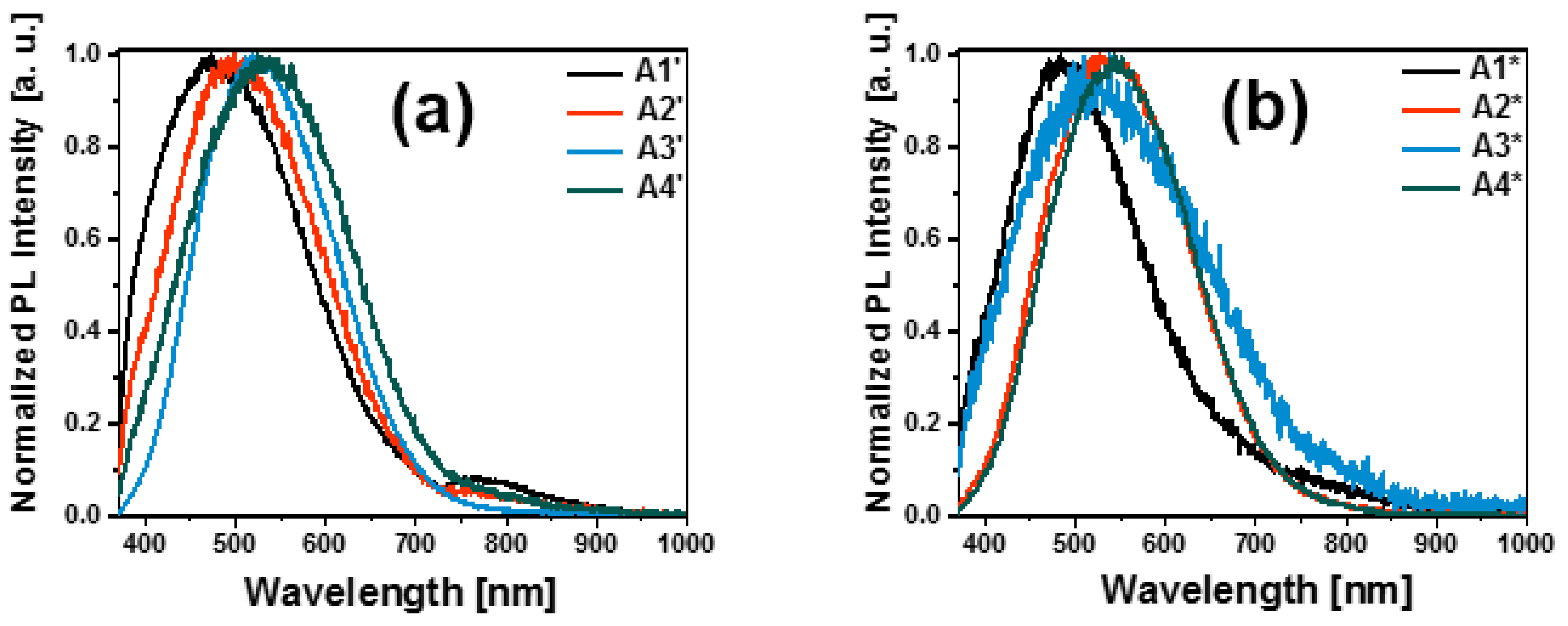
| 75.75 mA/cm2 Anodizing Current Density | |||
|---|---|---|---|
| Etching Time | Sample | With CNTs | With GO |
| 120 s | A1 | A1′ | A1* |
| 240 s | A2 | A2′ | A2* |
| 360 s | A3 | A3′ | A3* |
| 480 s | A4 | A4′ | A4* |
| 75.75 mA/cm2 Anodizing Current Density | |
|---|---|
| Etching Time [s] | Band Gap Energy [eV] |
| 120 | 1.89 |
| 240 | 1.97 |
| 360 | 2 |
| 480 | 2.01 |
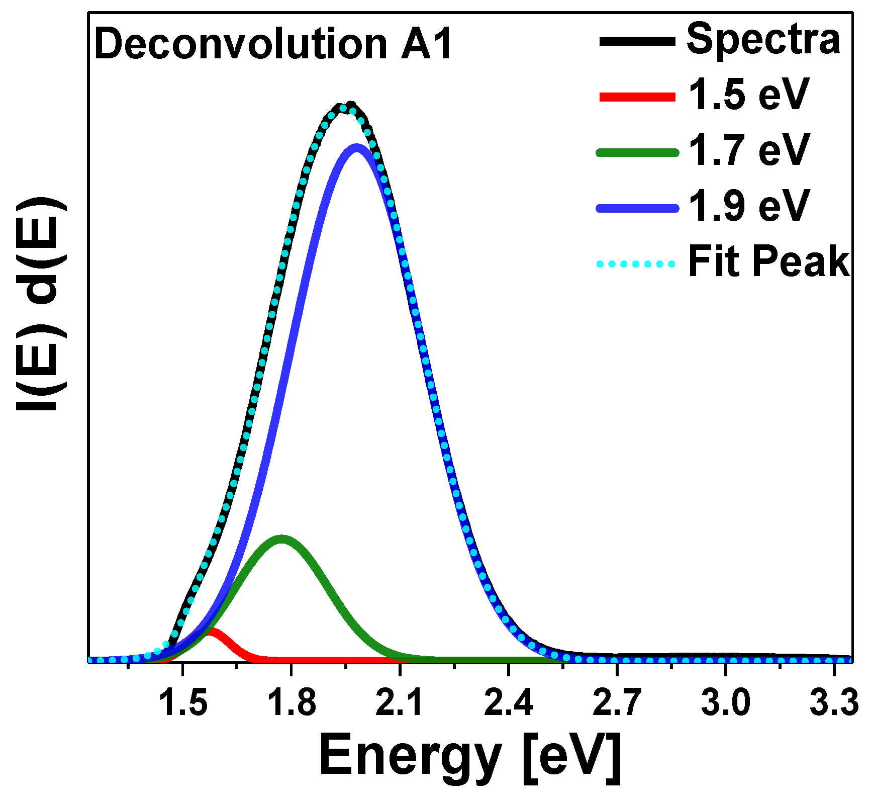
| Sample | S Band | ||
|---|---|---|---|
| A1 | 1.98 | 1.77 | 1.57 |
| A2 | 2.04 | 1.78 | 1.57 |
| A3 | 2.07 | 1.81 | 1.57 |
| A4 | 2.09 | 1.87 | - |
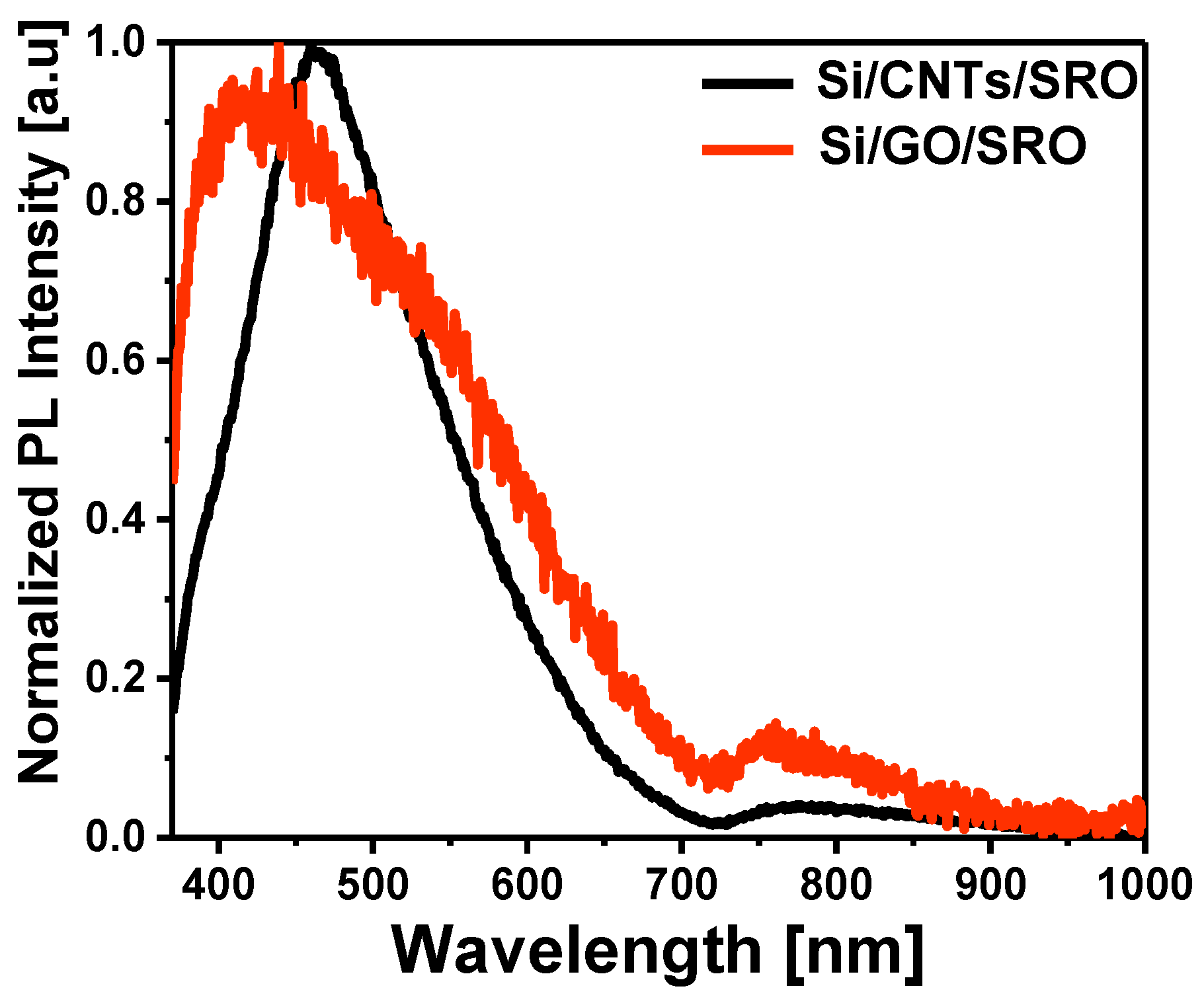
| Si-n/CNTs/SRO PL Emission Mechanisms | Si-n/GO/SRO PL Emission Mechanisms | ||
|---|---|---|---|
| Luminescent centers associated with diamond films | 2.7 [40] | It is attributed to the excimer present in the GO | 3 [41] |
| Defects due to Nitrogen | 2.4 [42] | Interactions between graphene planes and OD (Oxidative debris) | 2.5 [41] |
| Non-bridging oxygen hole centers (NBOHC) | 1.6 [43] | Non-bridging oxygen hole centers(NBOHC) | 1.6 [43] |
| Si-n/PSi/CNTs/SRO PL Emission Mechanisms | ||||
| A1′ | A2′ | A3′ | A4′ | |
| Luminescent centers associated with diamond films [40] | 2.8 | 2.8 | 2.7 | 2.8 |
| Defects due to Nitrogen [42] | 2.4 | 2.5 | 2.4 | 2.5 |
| PSi band gap | 2.1 | 2.2 | 2.1 | 2.1 |
| Non-bridging oxygen hole centers [42] | 1.7 | 1.7 | 1.7 | 1.7 |
| Si-n/PSi/GO/SRO PL emission mechanisms | ||||
| A1* | A2* | A3* | A4* | |
| It is attributed to the excimer present in the GO [41] | 3.1 | - | - | - |
| Graphene oxide quantum dots [46] | 2.8 | 2.8 | 2.8 | 2.7 |
| Interactions between graphene planes and OD [44] | 2.4 | 2.4 | 2.4 | 2.4 |
| Porous silicon band gap | 2.1 | 2.2 | 2 | 2.1 |
| Non-bridging oxygen hole centers [42] | 1.7 | 1.8 | 1.6 | 1.7 |
Disclaimer/Publisher’s Note: The statements, opinions and data contained in all publications are solely those of the individual author(s) and contributor(s) and not of MDPI and/or the editor(s). MDPI and/or the editor(s) disclaim responsibility for any injury to people or property resulting from any ideas, methods, instructions or products referred to in the content. |
© 2023 by the authors. Licensee MDPI, Basel, Switzerland. This article is an open access article distributed under the terms and conditions of the Creative Commons Attribution (CC BY) license (https://creativecommons.org/licenses/by/4.0/).
Share and Cite
Mendoza Conde, G.O.; Luna López, J.A.; Hernández Simón, Z.J.; Hernández de la Luz, J.Á.D.; Monfil Leyva, K.; Carrillo López, J.; Martínez Hernández, H.P.; Gastellóu Hernández, E.; Berman Mendoza, D.; Flores Méndez, J. Nanocomposites of Silicon Oxides and Carbon: Its Study as Luminescent Nanomaterials. Nanomaterials 2023, 13, 1271. https://doi.org/10.3390/nano13071271
Mendoza Conde GO, Luna López JA, Hernández Simón ZJ, Hernández de la Luz JÁD, Monfil Leyva K, Carrillo López J, Martínez Hernández HP, Gastellóu Hernández E, Berman Mendoza D, Flores Méndez J. Nanocomposites of Silicon Oxides and Carbon: Its Study as Luminescent Nanomaterials. Nanomaterials. 2023; 13(7):1271. https://doi.org/10.3390/nano13071271
Chicago/Turabian StyleMendoza Conde, Gabriel Omar, José Alberto Luna López, Zaira Jocelyn Hernández Simón, José Álvaro David Hernández de la Luz, Karim Monfil Leyva, Jesús Carrillo López, Haydee Patricia Martínez Hernández, Erick Gastellóu Hernández, Dainet Berman Mendoza, and Javier Flores Méndez. 2023. "Nanocomposites of Silicon Oxides and Carbon: Its Study as Luminescent Nanomaterials" Nanomaterials 13, no. 7: 1271. https://doi.org/10.3390/nano13071271