3.1. ZnO Growth Mechanism and Morphologies
As the ZnO-growth process is highly dependent on the complex combination of process parameters, e.g., system geometry (tube diameter) [
21], temperature (
T) [
14], gas composition [
15], and flow [
15,
22], pressure [
21], type of substrate [
23] and catalyst [
12], the morphology expressions depend on the growth-setup. To differentiate between effects concerning the ZnO growth induced by the process parameters and those from laser irradiation of the catalytic gold thin film, ZnO-nanostructures were generated on unirradiated Au thin films with different layer heights (0.6–5.4 nm). Details about the thermal chemical vapor deposition (t-CVD) process are explained in detail in the
Section 2.
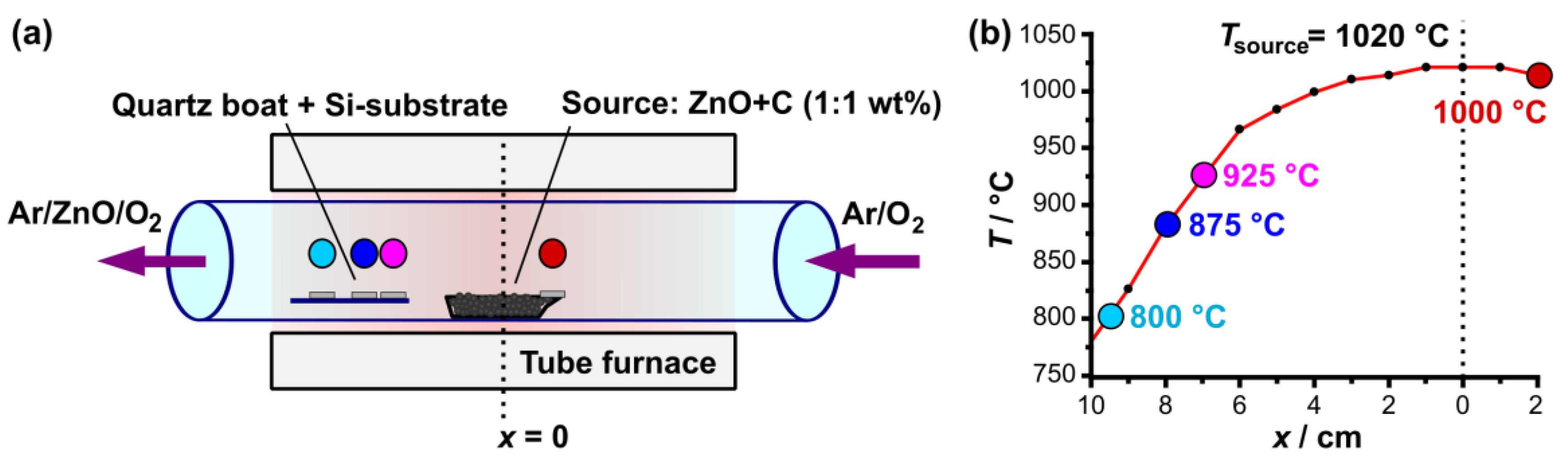
Figure 2a shows ZnO-nanostructures generated in a pure Ar–atmosphere (
p = 12 mbar) at different temperatures
T (hence different distances to the Zn-source, growth time
t = 10 min). ZnO growth in pure Ar-atmosphere results in ZnO-nanorods (NRs) for all examined temperatures and gold layer heights. Analogue SEM micrographs for
T = 1000 °C (upstream) are illustrated in the
SI (Figure S3). The width and length of the NRs are dependent on the growth temperature. Lower temperatures lead to thicker, but shorter, NRs. Upon introducing 1% O
2 to the carrier gas, a mixture of different morphologies consisting of thin nanowires (NWs) and narrow nanobelts (NBs) are obtained at
T = 800 °C (
Figure 2b). The colors in
Figure 2 match the temperatures and sample positions illustrated in
Figure 1.
The vapor-liquid-solid (VLS) growth process is characterized by gold nanoparticles [
12] forming liquid Au-Zn catalyst droplets, resulting in tip growth of nanostructures from precipitated ZnO [
11]. For the liquid-solid (VS) mechanism, the Zn directly reacts to ZnO at the surface, resulting in ZnO bases (root growth). Although the presence of a noble metal catalyst is not inherently necessary, the metallic nanoparticles act as energetically favored nucleation sites for the Zn-vapor [
24]. Both growth mechanisms are explained in detail in the
SI (Section S2). In
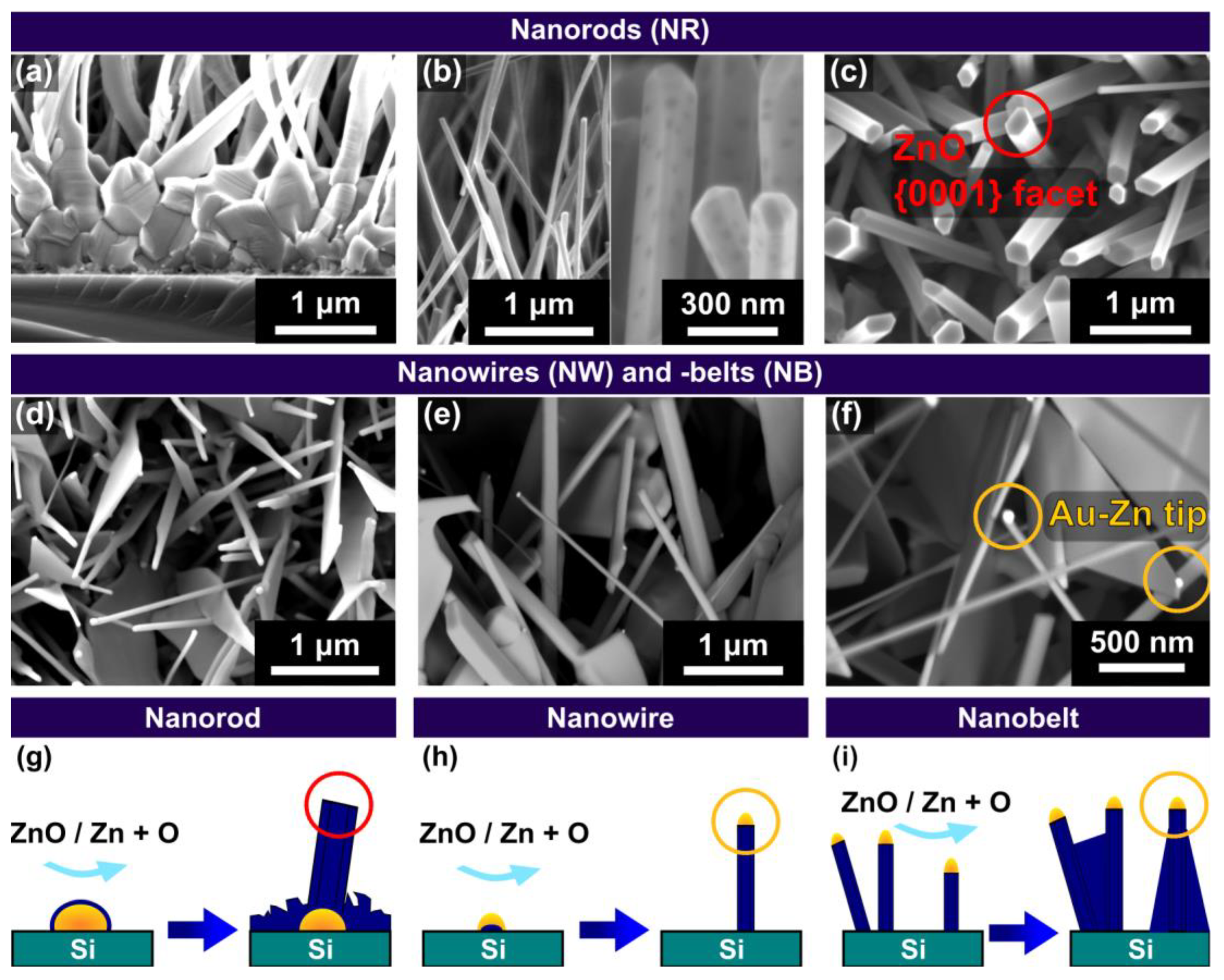
Figure 3 the three main types of ZnO-nanostructure morphologies grown in our setup, i.e., nanorods (NRs, 1D), nanowires (NWs, 1D) and nanobelts (NBs, 2D), are exemplarily displayed. ZnO-NRs (
Figure 3a–c) grow from a ZnO base layer formed by the VS mechanism, as schematically illustrated in
Figure 3g. As a consequence, the NRs tip consists of {0001}-facets (
Figure 3c), typical for the preferential c-plane growth ([0001]-direction) of the strongly anisotropic wurtzite crystal structure of ZnO [
11]. NWs (
Figure 3d–f) grow by the VLS mechanism, thus a gold particle is observed at their tip, as highlighted in
Figure 3f and schematically represented in
Figure 3h. NBs (
Figure 3d–f) represent a two-dimensional ZnO growth, induced by excess Zn atoms, not dissolved in gold nanoparticles, leading to a growth of the sides of NWs. This growth is often initiated at the junction of two NWs as illustrated in
Figure 3i [
14].
We want to emphasize that although we designated the term NRs to VS-grown nanostructures and NWs to VLS-grown nanostructures to match the occurring morphologies for our growth conditions, in general, both mechanisms can lead to very thin (wire-like) and broad, faceted (rod-like) nanostructures. Comparing the morphology occurrence shown in
Figure 2 with the growth mechanism assignments illustrated in
Figure 3, it is obvious that a pure Ar-atmosphere leads to complete dominance of the VS mechanism, while the addition of O
2 leads to a concurrent VS and VLs ZnO growth. This finding needs to be considered while investigating the growth of ZnO nanostructures on laser-generated catalysts. For further nanostructure characterization,
Figure S4 (SI) shows an exemplary EDX measurement of ZnO nanostructures. All experiments compromising laser irradiation shown in the following part of the work were conducted on samples with a gold film thickness of 2.8 nm, representing a medium value of the explored thin film thickness range (
Figure 2).
3.2. Au Catalyst Generation by Laser Irradiation
ZnO nanostructures grown on unirradiated samples, as discussed in the previous
Section 3.1, display a shortcoming of the common (t-CVD) induced semiconductor growth. The substrate is homogeneously covered with similar noble metal catalysts, thus not allowing the growth of different ZnO nanostructure types on a single substrate. In literature, the spatial-selective generation of semiconductor growth is demonstrated, but again only by binary growth control [
19,
20,
25,
26]. To address this limitation we used pulsed laser-induced dewetting (PLiD) of the gold thin films before the thermally induced dewetting and ripening occurring in the ZnO growth process. Dewetting fragmentizes existing nanoparticles or -structures and ripening leads to the growth of one particle at the expense of others (by material transfer), all affecting the Au catalyst sizes. The scan strategy for areal-irradiation of the Au@Si-systems consists of a meandering scan path as explained in detail alongside the laser setup in the
SI (Figure S2).
Upon laser irradiation, multiple effects generating or modifying gold nanoparticles occur. At the lowest laser energies, the initial thin film layer is dewetted by (PLiD). Striving for the lowest surface energy, the film fragmentizes into smaller gold patches and nanoparticles. This matter reorganization is mediated through thin film and filament instabilities and results in the formation of increasingly smaller Au nanoparticles. To ensure the nanoparticle formation to be as homogenous as possible, we conducted all experiments using circularly polarized laser pulses. As a consequence, the formation of one-dimensional laser-induced periodic surface structures (1D-LIPSS) is suppressed. Nevertheless, 2D-LIPSS consisting of periodic arrays of relatively large, periodically arranged Au nanoparticles are formed at higher energy doses [
27]. 2D-LIPSS nanoparticles are fully covered with a thin SiO
2 layer and partly sunken in the silicon. Before the formation of the highly arranged 2D-LIPSS, their predecessor structures are formed. These Au nanostructures are not periodically arranged but are covered with a thin SiO
2 passivation layer and are partly sunken into the silicon wafer too. At high laser energy doses, laser ablation of Au leads to the formation of a plasma. During the thermal relaxation following laser irradiation, the condensation of the aforementioned Au plasma leads to the formation of small nanoparticles. Unlike most other gold particles in this laser energy regime, these nanoparticles are not passivated by a SiO
2 layer and are located on the sample’s surface. For all mentioned effects, the Au catalyst generation is schematically represented in
Figure 4. PLiD, 2D-LIPSS generation, and the formation of small Au nanoparticles by condensation are extensively described in Durbach et al. [
27]. The referenced work additionally illustrates the embedment of the various nanoparticles types in the substrate. Further explanations on the formation and properties of the passivating SiO
2 layer are presented in
Section 3.4.
As the passivation of the Au nanostructures has significant implications on the ZnO growth, we classified the laser-generated nanoparticles into two categories. The first category consists of passivated nanoparticles, covered with a thin SiO
2 layer and partly sunken in the Si-wafer, e.g., 2D-LIPSS and their predecessor structures. They are further referred to as pNPs (passivated nanoparticles). The second category of nanoparticles consists of exposed nanoparticles (eNPs) and includes particles generated by PLiD, as well as particles formed by Au plasma condensation. The sum of all presented laser-induced effects results in an initially increasing proportion of passivated Au. Due to laser ablation and recondensation of Au nanoparticles, this trend is reversed for the highest laser energy doses, e.g., effective pulse number
N, as illustrated in
Figure 4.
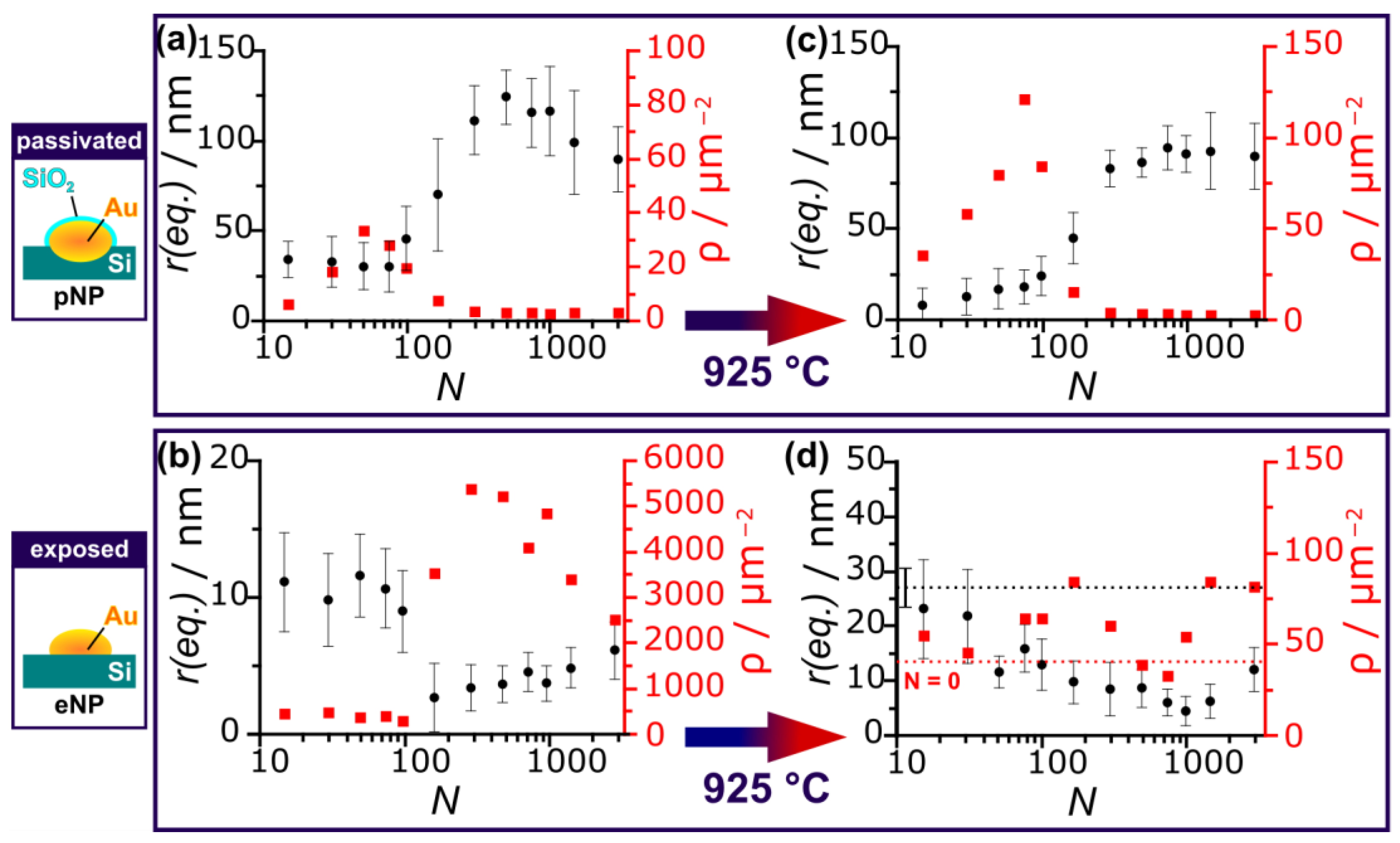
The size and area density of both particle types were extracted from SEM images obtained by different detectors, as described in detail in the
SI (Figure S5). To ensure comparability for uneven Au nanostructure shapes, the sizes are indicated by an equivalent to the radius of perfectly round particles possessing the same area. In
Figure 5 the equivalent radius
r(eq.) (black) and the area particle density
ρ (particle count per area, red) are shown for particles generated by areal-irradiation using different effective pulse numbers
N, a line-to-line distance (hatch) of
h = 3.3 µm, a pulse fluence of
= 127 mJ/cm
2 and a pulse frequency of
f = 100 kHz. As ZnO-growth takes place at high temperatures, we examined the nanoparticle’s ripening and dewetting mediated by the temperatures present during the heating phase of the ZnO-growth process. A blank growth cycle, analog to the regular ZnO growth process, but using only trace amounts of ZnO/C, was conducted. As such the process conditions relevant to dewetting and ripening of the nanoparticles were controlled. The ZnO nanostructure growth was consequently inhibited, while still allowing preliminary ZnO-nucleation and Au-Zn alloying. This method enables a detailed study of the active catalyst particles and the temperature-mediated changes to
r(eq.) and the area density
ρ are observed by comparing
Figure 5a/b to
Figure 5c/d. The dashed lines in
Figure 5d represent the values concerning Au particles generated only by heat-induced dewetting (unirradiated:
N = 0).
Passivated nanoparticles (pNPs,
Figure 5a) show a particle density peaking at about
N = 50 (
= 127 mJ/cm
2). For higher
N the particle density converges to a value of about 3 particles/μm
2 as a result of the self-regulated 2D-LIPSS formation. Upon increasing
N the size of 2D-LIPSS nanoparticles increases to a maximum of ~124 nm (
N = 498) before slightly diminishing, as expected for LIPSS generation [
28]. This decrease in the pNPs’ size is explained by the partly ablation of the gold layer upon high energy doses, leading to the formation of small re-condensed Au-NP. At temperatures of 925 °C the pNPs undergo thermal dewetting, resulting in an increased count of smaller pNPs. Particles generated in the 2D-LIPSS generation parameter range, e.g., greater than
N = 100 for
= 127 mJ/cm
2, are relatively unaffected by the heating process, as they are well separated by the prior self-organization process. Exposed nanoparticles (eNPs,
Figure 5b) show fairly constant particle sizes and densities for
N smaller than 100, with an increase in the particle density by an order of magnitude and initial size drop for effective pulse numbers
N greater than 100. This binary particle formation results from the aforementioned Au condensation from ns-laser laser ablation-generated plasma. Upon increasing
N, the particle sizes (
r(eq.)) decline constantly starting from a value of 27.1 nm for unirradiated samples. For the highest pulse numbers, a slight increase of
r(eq.) is observed. After heating, the areal density
ρ(eNPs) initially increases upon increasing
N due to a dewetting process. After this initial increase, a dip in the particle density is observed. This laser parameter regime is optimal for 2D-LIPSS formation, resulting in an overall maximal proportion of Au residing in pNPs. Additionally,
ρ(eNPs) the high particle density allows for additional particle fusing/ripening.
In conclusion, progressively more Au is allocated to pNPs upon increasing
N, leading to an increase in their size. As pNPs generated with higher
N are already in a favorable energetic state, they are relatively unaffected by the heating process. The interplay of the dewetting of the initial thin film, emerging nanoparticles from laser ablation and thermal ripening, results in the density of eNPs fluctuating in a range of 40–80 particles/μm
2, while their size shrinks. Only for the highest energy doses, a slight increase of
r(eq., eNPs) is observed. Overall the size and area density of pNPs and eNPs are consistent with expectations concerning all laser irradiation effects summarized in
Figure 4 and the subsequent thermal treatment.
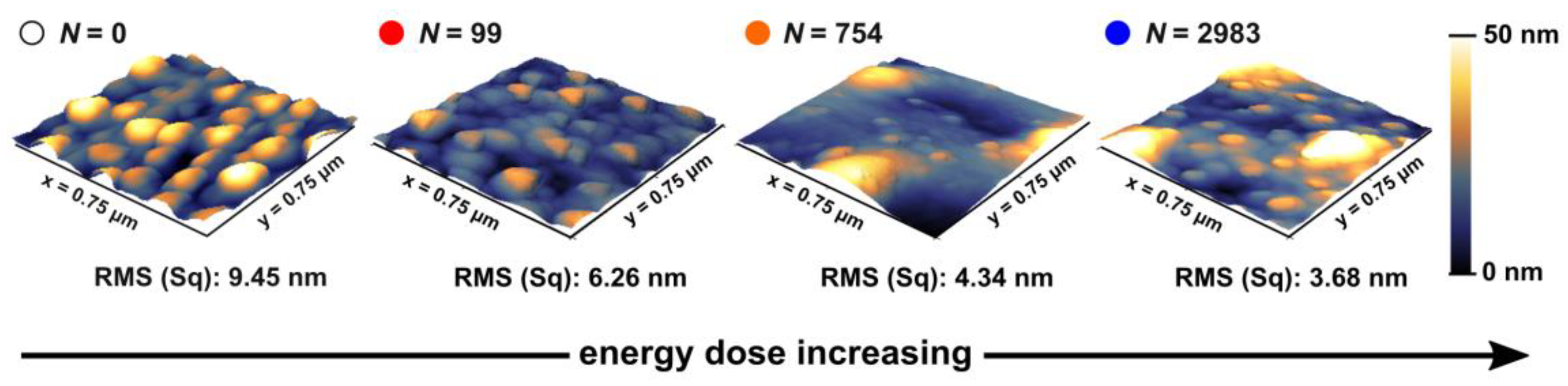
Atomic force microscopy (AFM) measurements were performed to acquire topographical images, as well as surface roughness information (RMS (sq.)), of the laser-modified catalysts for selected effective pulse numbers
N. (
Figure 6). The colored markers help to associate the data across several figures (
Figure 6,
Figure 7,
Figure 8 and
Figure 9). Note that for
N = 745 and
N = 2983 the roughness calculation was performed in the interstitial space between 2D-LIPSS to omit the relatively long-ranged surface modulation induced by the 2D-LIPSS formation (periodicity of ca. 510 nm), which is not assumed to have any notable effect on the ZnO nucleation. As for the reduction of the RMS values upon increasing
N, less favorable nucleation for the Zn vapor on irradiated surfaces is expected. As a consequence, VS growth is inhibited.
3.3. ZnO Growth on Laser-Generated Catalysts
Concerning the root growth (VS) of ZnO nanostructures, Chandrasekaran et al. [
29]. attributed the diameter of NRs/NWs to be dependent on the temperature
T, the ratio of the semiconductor (e.g., Zn) at the interface, and the interfacial energy
σ. The surface particle curvature [
30], being a function of
r(eq.), and the surface roughness (RMS) [
31] are both affected by laser irradiation, as investigated in
Section 3.2. Consequently, all laser-irradiated catalysts show altered surface energies, i.e., nucleation properties, and are assumed to directly affect ZnO growth.
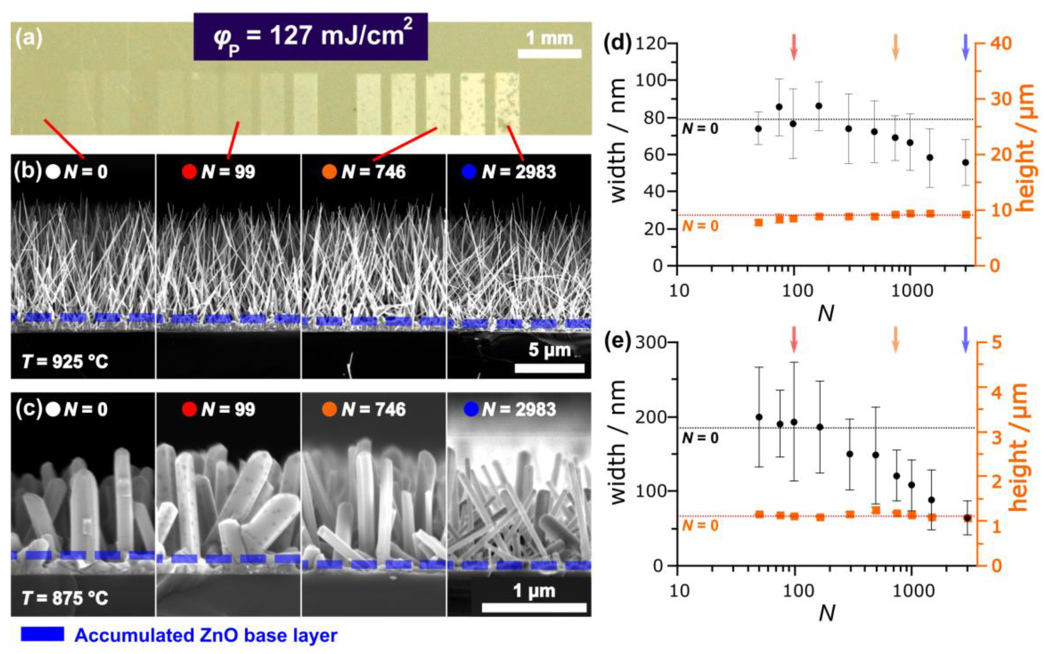
Figure 7a,b shows an optical image and cross-sectional SEM images of ZnO-NRs respectively (Ar,
T = 925 °C,
t = 10 min).
Figure 7c shows analogous cross-section micrographs of shorter, but wider ZnO-NRs grown at a lower temperature
T = 875 °C. In
Figure 7d/e the width (black) and height (orange) of the NRs from
Figure 7b/c are shown. While the height (orange) remains relatively constant and similar to those grown on unirradiated samples (
N = 0), a significant decrease in the NRs´ width (black) can be observed upon increasing
N. Comparing the NRs´ width with the particle analysis data shown in
Figure 5, the pNPs seem to have no significant influence on the VS-grown NRs. In contrast, the decrease in the NR’s-width (upon increasing
N) correlates strongly with the diminishing of
r(eq., eNPs). Likewise, the error bars, narrowing for
r(eq., eNPs), correlate to more uniformly grown NRs (smaller error bars,
Figure 7d,e). Although the VS mechanism responsible for the growth of NRs does not inherently require the presence of a gold catalyst, the exposed Au surface of the eNPs seems to be most influential for the ZnO growth. The Au surface is the energetically favored nucleation site [
24]. An additional growth of a thick ZnO accumulated base layer (marked with blue dashed lines in
Figure 7b,c and magnified in
Figure 3a) is observed. This layer´s height diminishes continuously upon increasing the effective pulse number
N, finely being barely visible for
N = 2983. Consequently, the pulsed laser-induced dewetting (PLiD) of the Au catalyst layer may not only lead to a gradual control of the NRs´ width but also to an improvement of the NRs´ homogeneity and reduction of ZnO accumulations at the wafer surface. The effect of the laser irradiation on the NRs´ width is most apparent for thicker NRs as depicted in
Figure 7c,e.
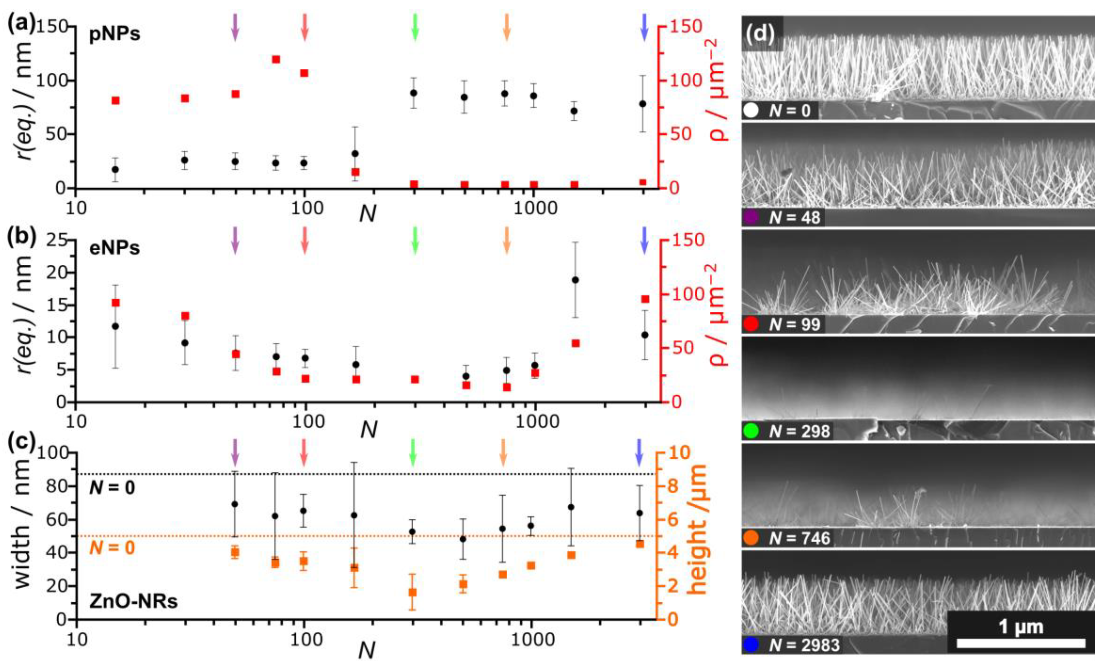
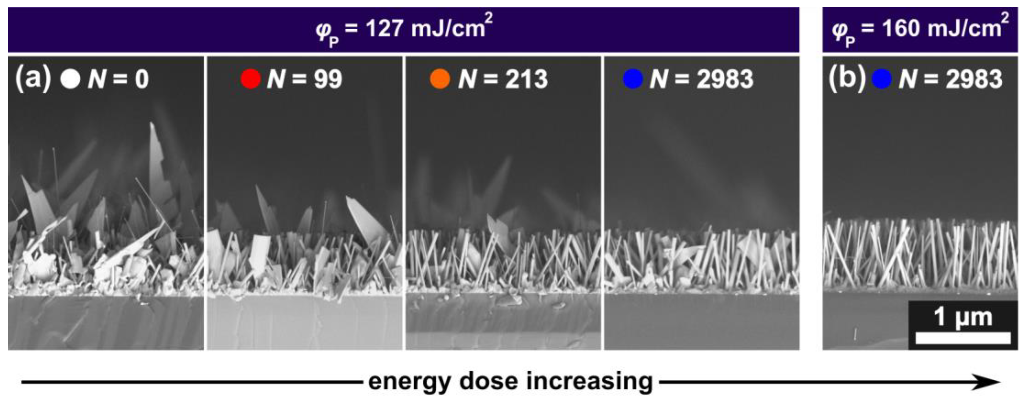
Figure 8a,b shows
r(eq.) and
ρ of laser-generated catalysts formed using a higher pulse fluence of
= 160 mJ/cm
2 and after heating (
T = 925 °C). In
Figure 8c the width and height of the corresponding ZnO-NRs are depicted. Similar to the laser irradiation with lower pulse fluences (
= 127 mJ/cm
2,
Figure 7), no noticeable effect of the pNPs on the ZnO-NRs´ growth or properties is observed, while the NRs´ growth is strongly influenced by the size of the eNPs. As aforementioned, the initial decrease of
r(eq.) and
ρ for eNPs is explained by the PLiD, while the re-increase is mediated by the condensation of Au from an ablation-induced plasma upon high laser energy doses. The higher pulse fluence of
= 160 mJ/cm
2 allows for a significant change in the ZnO-NR density, induced by the significant decline of
ρ(eNPs) and thus resulting in a nearly complete suppression of ZnO growth for
N = 298 (
Figure 8d). The suppression of VS-mediated ZnO growth is assumed to be also a consequence of the SiO
2 layer formation.
The ZnO-NR growth shown above is dominated by the root-growth mechanism (VS), i.e., mediated by the surface’s eligibility as a nucleation site (surface energy
σ). In contrast, the VLS process is mediated by a gold catalyst, alloying Zn from the environment and forming a ZnO-NW at its bottom (tip growth). As a consequence, the temperatures and the partial gas pressures at the substrate need to be in the correct range to allow Zn supersaturation and Au-Zn alloy formation. As discussed in
Section 3.1, VLS-mediated ZnO growth was achieved by changing the partial gas pressures upon adding 1% of O
2 to the Ar carrier gas. To obtain the nanostructures shown in
Figure 9, samples were prepared and irradiated analogously as those shown in
Figure 7 and
Figure 8 and placed in the furnace using growth parameters favoring the VLS-growth mechanism (Ar + 1% O
2,
T = 800 °C,
t = 10 min). Upon increasing the laser energy dose, a steep decline in the occurrence of VLS-grown ZnO nanostructures (NWs, NBs) is observed in the cross-sectional SEM images shown in
Figure 9.
The VLS growth is suppressed by two distinct laser-induced mechanisms. First of all the passivated 2D-LIPSS and their predecessors (pNPs) are partly sunken in the silicon wafer [
27] and therefore bound to the substrate, impeding the ability of the catalyst to lift-off away from the surface and consequently inhibiting tip growth (VLS). Although not covered by a SiO
2-layer, Au nanoparticles generated by laser ablation and recondensation are slightly embedded in the underlying SiO
2 layer, also inhibiting a lift-off. For thermally dewetted metals, this interaction of the metallic nanoparticles with the substrate is commonly assigned to the contact angle [
13]. Furthermore, laser irradiation leads to the formation of small Au nanoparticles (
Figure 5 and
Figure 7). For VLS growth the precursor activity needed to fulfill the necessary chemical potential is hardly ever reached for nanoparticles with a diameter smaller than 10 nm [
32]. This critical particle diameter matches the smallest laser-generated particles in this work. Appropriate to both assumed VLS impeding mechanisms,
Figure 9 shows the decrease in VLS-grown structures, i.e., the occurrence of NWs and NBs, upon higher laser energy doses. Incidentally, this also leads to a decrease in the overall ZnO nanostructure height, as VLS-grown nanostructures overgrow ZnO-NR as seen in
Figure 9 for
N = 0.
3.4. Effects of the Laser-Induced SiO2 Layer
Additionally to the well-examined nanosecond (ns)-laser-induced changes for the Au catalysts, a change in the Si-surface through amorphization and oxidation, occurring during the 2D-LIPSS generation (ca.
N > 100), may further influence the interfacial energy σ [
27,
28]. The laser-induced formation of a passivating SiO
2 layer, well-known in ns-laser LIPSS formation literature [
27,
33,
34], plays a significant role in the laser pulse-modified growth of ZnO nanostructures. A detailed description of the SiO
2-layer and corresponding EDX analysis can be found in Reinhardt et al. [
34]. The SiO
2 layer existing on pNPs inhibits Au-Zn alloy formation and thus prevents the growth of VLS-induced ZnO-nanostructures. Simultaneously the roughness and surface energy are altered, consequently affecting the ZnO nucleation (VS). In
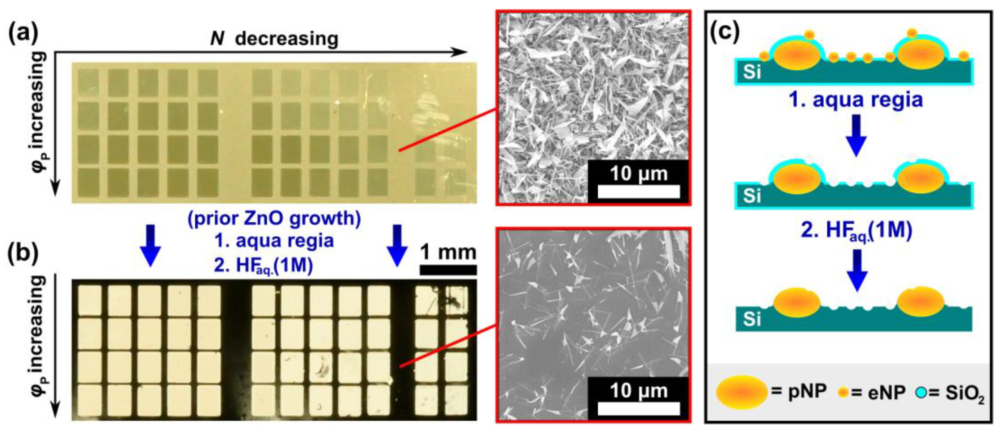
Figure 10a a photograph of a Si-wafer, irradiated with different laser parameters, is displayed after ZnO-growth.
Figure 10b shows an identically prepared Si-wafer, immersed in freshly prepared aqua regia (nitro-hydrochloric acid: 1:3 HNO
3:HCl, 30 s) and subsequently immersed in hydrofluoric acid (HF, 1M, 60 s), before the ZnO growth process. The etching-process results in the removal of eNPs in the first and the removal of the SiO
2 layer in the second step, laying bare the pNPs, e.g., 2D-LIPSS. The effects of both consecutive etching steps are schematically illustrated in
Figure 10c. Contrarily to the untreated wafer seen in
Figure 10a, the etched sample shows hardly any growth of ZnO nanostructures at unirradiated areas, as the gold thin film, acting as a catalyst, is completely removed. ZnO-nanostructures, seen as bright areas in
Figure 10b, grow on the laid bare gold particles (formerly pNPs) situated at irradiated areas. Therefore ZnO growth is seen even for the lowest energy dose used in this work (top right corner of the substrate,
= 112 mJ/cm
2,
N = 15). The same etching technique allows for a spatially controlled growth of ZnO-nanostructures, as it removes the Au catalysts in all unirradiated areas, while the formerly passivated nanoparticles (pNPs) reside and are now exposed. This oppositional ZnO growth behavior can be further observed in a video of the growth process of untreated (left) and etched (right) samples at different temperatures
(SI, Video S1). It should be noted, that the bonding of these exposed, formerly passivated nanoparticles to the substrate, only allow for VS-growth for the growth setup used in this work.
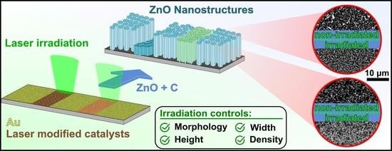
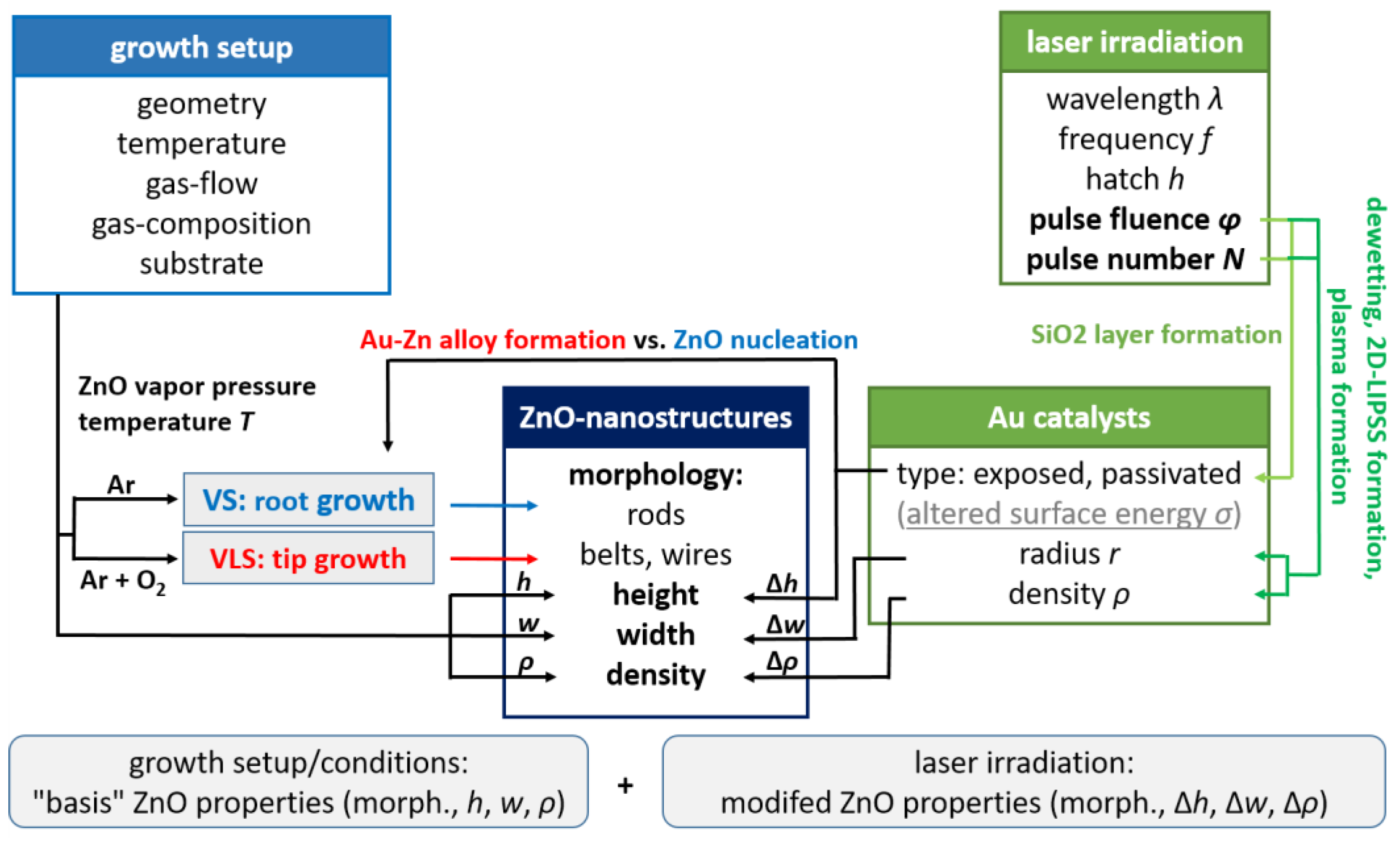
3.5. Overview of Laser-Irradiation’s Effects on ZnO Growth
As both, the laser-induced generation of gold catalysts and the subsequent ZnO growth compromise a plethora of different effects, the laser irradiation’s ability to affect ZnO growth should be recapitulated by highlighting the most important contributory factors. In general, the growth setup and the growth conditions determine the partial gas pressures of the reactive species in the vicinity of the substrate. Growth conditions are thus set for the entirety of the substrate, leading to predetermined ZnO nanostructure properties, e.g., morphology, height, width, and density. Laser irradiation of the Au surface before ZnO growth allows the generation of different Au catalysts. Depending on the laser parameters, e.g., pulse number
N and pulse fluence
, the size, density, and type of the laser-generated catalysts can be spatial-selectively controlled. For the system of Au@Si used in this work, two distinct types of Au-catalysts are generated. A part of the Au nanostructures is passivated with a thin SiO
2 layer and/or partly embedded in the substrate. As a consequence, the surface energy
σ and predisposition for Au-Zn alloy formation, and therefore the VS and VLs growth mechanisms, are altered locally (
Figure 9). Likewise, the density and size of the catalyst (
Figure 4 and
Figure 5) have similar influences on the ZnO nanostructures’ width or density (
Figure 7 and
Figure 8). These parameters are a function of the applied laser energy dose. In
Figure 11 the key aspects of the aforementioned interplay of ZnO growth conditions and the laser irradiation’s effects are schematically summarized.
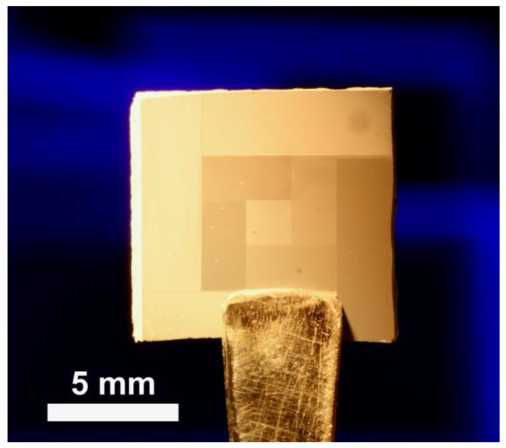
The spatial-selective and gradual change of the irradiated areas is evident by observing the different shades, corresponding to macroscopic optical properties, shown for a ZnO-covered Si-wafer in
Figure 12. Complementary,
Figure S6 (SI) shows an overview of the boundary of an irradiated and unirradiated ZnO-overgrown area, illustrating the effect of the irradiation on the ZnO-NRs’ width and ZnO morphology-occurrence. The nanosecond laser-induced generation of Au catalysts shown in this work establishes a proof of principle for a maskless, controllable manipulation of ZnO nanostructures. By adjusting the irradiation conditions the presented principles are expected to be expandable to a variety of substrate materials. Likewise, a variation in the thickness of the underlying SiO
2-layer could lead to additional growth control. By allowing better control of the growth mechanism, e.g., by changing to a pure Zn-source, the laser-induced changes to the VLS growth should become even more apparent. The control of ZnO properties achieved in this work may be explored for complex ZnO nanostructure designs for opto-electrical devices.


