Article

The Combined Effects of an External Field and Novel Functional Groups on the Structural and Electronic Properties of TMDs/Ti3C2 Heterostructures: A First-Principles Study

1
College of Aerospace and Civil Engineering, Harbin Engineering University, Harbin 150001, China
2
School of Physics and Engineering, Sun Yat-sen University, Guangzhou 510275, China
*
Author to whom correspondence should be addressed.
Nanomaterials 2023, 13(7), 1218; https://doi.org/10.3390/nano13071218
Submission received: 16 February 2023 / Revised: 22 March 2023 / Accepted: 28 March 2023 / Published: 29 March 2023

Abstract

:
The stacking of Ti3C2 with transition metal dihalide (TMDs) materials is an effective strategy to improve the physical properties of a single material, and the tuning of the related properties of these TMDs/Ti3C2 heterostructures is also an important scientific problem. In this work, we systematically investigated the effects of an external field and novel functional groups (S, Se, Cl, Br) on the structural and electronic properties of TMDs/Ti3C2X2 heterostructures. The results revealed that the lattice parameters and interlayer distance of TMDs/Ti3C2 increased with the addition of functional groups. Both tensile and compressive strain obviously increased the interlayer distance of MoS2/Ti3C2X2 (X = S, Se, Cl, Br) and MoSe2/Ti3C2X2 (X = Se, Br). In contrast, the interlayer distance of MoSe2/Ti3C2X2 (X = S, Cl) decreased with increasing compressive strain. Furthermore, the conductivity of TMDs/Ti3C2 increased due to the addition of functional groups (Cl, Br). Strain caused the bandgap of TMDs to narrow, and effectively adjusted the electronic properties of TMDs/Ti3C2X2. At 9% compressive strain, the conductivity of MoSe2/Ti3C2Cl2 increased significantly. Meanwhile, for TMDs/Ti3C2X2, the conduction band edge (CBE) and valence band edge (VBE) at the M and K points changed linearly under an electric field. This study provides valuable insight into the combined effects of an external field and novel functional groups on the related properties of TMDs/Ti3C2X2.

Graphical Abstract

1. Introduction

Due to the inter-layer coupling effect, heterostructures formed by vertically stacking different two-dimensional (2D) materials can achieve ultra-high-performance improvements and possess unprecedentedly excellent physical properties [1,2,3]. The transition metal dihalides (TMDs) have excellent band gap widths in the range of 1.0 eV to 2.0 eV [4]. The monolayer MoS2, as a typical representative member of the most studied TMD family, is a semiconductor material with a direct band gap of 1.8 eV, and it is widely used in logic transistors and photodetector devices [5,6]. Similarly, the monolayer MoSe2, as another important member of TMDs, has many promising applications in electronics and optoelectronics due to its unique electronic, optical, mechanical, chemical, and thermal properties [7,8]. However, TMDs also have some negative properties that affect their application. For example, their carrier effective mass is relatively high, while the carrier mobility is very low [9,10], which hinders their application in high-performance nanodevices. Several studies have shown that the heterogeneous structures formed by stacking TMDs with other 2D materials can significantly modulate the structural, electronic, and mechanical properties of TMDs. For example, the studies of Biroju et al. [11] showed that MoS2 stacked with a bilayer graphene heterostructure can improve electronic conductivity, electrochemical properties, and photochemical properties. Li et al. [12] systematically investigated electron density differences and band gaps of Cu3N/MoS2 heterostructures, and the results showed that the charge was mainly accumulated and consumed near the atoms, with only a small amount of charge accumulating between the layers, and the bandgap of Cu3N/MoS2 heterostructures can be efficiently tuned with the variation of the interlayer distance. Moreover, Cu3N/MoS2 heterostructures have a stable structure and excellent photoelectric properties. Celal et al. [13] investigated the structural and electronic properties of GaN/MoSe2 heterostructures with van der Waals (vdW) correction. An indirect band gap of 1.371 eV was obtained when the GaN monolayers were adsorbed on MoSe2 monolayers, while when GaN was stacked on MoSe2 monolayers, the indirect band gap in GaN monolayers was maintained at 0.341 eV. Based on these studies, we can conclude that combining TMDs with other two-dimensional layered materials to form heterogeneous structures may be an effective way to tune and improve the relevant properties of TMDs.
MXenes are a new and important member of the family of 2D materials discovered in recent years and are complex layered 2D material systems representing a large class of transition metal nitriles, carbides, and carbonitrides [14,15,16]. Ti3C2 is a typical transition metal carbide with multilayer metal ion adsorption behavior, with ultra-high electrical conductivity and extraordinary mechanical and electronic properties [17,18]. Ti3C2 is expected to be the most competitive material candidate in some fields, such as high-performance ultra-thin electronics and storage [19,20]. Mathis et al. [21] investigated the MXene nanosheets (Al-Ti3C2), and found they have higher quality, increased oxidation resistance, and electronic conductivity increased to 20,000 S/cm. Al-Ti3C2 is a promising electric nanodevice. Li et al. [22] systematically investigated the interfacial properties of monolayer WS2 in contact with a series of MXenes using first-principles calculations. The results showed that Ti3C2 couples strongly with WS2, leading to the metallization of monolayer WS2 and the formation of ideal Ohmic contacts in the vertical direction. Moreover, during the electrode fabrication process, the face-to-face stacking of 1 nm thickness MXene limits the accessibility to electrolyte ions [23,24], which hinders the electronic properties utilization of its surface. For Ti3C2, heterostructure stacking is also a valuable tool for improving the electronic properties since it can not only add the excellent properties of a single 2D material but also provide a stable gallery space [25,26,27], which could prevent face-to-face stacking of MXene. For example, Wu et al. [28] systematically investigated the energy storage and electronic properties of N-Ti3C2/NiCo2S4 heterostructures. Owing to the unique heterostructure and friendly interfacial interaction, the N-Ti3C2/NiCo2S4 heterostructure had a stable structure, low internal resistance, and excellent rate performance. Debow et al. [29] found that the strong electronic coupling between Ti3C2Ox and TiO2 is due to their proximity; the Ti3C2Ox-generated electrons are transferred into the conduction band of the TiO2 semiconductor over the Schottky barrier with a fast time constant of 180 fs, leading to an increase in conductivity.
Currently, there are a large number of studies on TMD and MXene heterostructures. Jing et al. [30] systematically investigated the structural and electronic properties of MoS2/Ti3C2Tx (T = OH, F and O) heterostructures, and the results showed that the MoS2/Ti3C2F2 heterostructure is an n-type Schottky contact and the Schottky barrier height (SBH) is 0.73 eV, while the MoS2/Ti3C2O2 heterostructure is a p-type Schottky contact with an SBH of 0.33 eV. Moreover, the tensile strain can effectively adjust the position of the conduction band edge (CBE) of MoS2, which leads to an effective reduction of the Fermi energy level pinning and SBH, thus allowing for Ohmic contact. Guan et al. [31] studied heterostructures composed of Ti3C2T2 (T = O and F atoms) and metallic MoS2 (1T phase) for lithium-ion battery (LIB) applications. The different surface functional groups in MXenes were found to significantly alter the redox reaction of Li atoms in the Ti3C2T2 and 1T-MoS2 interfaces. The diffusion curve became significantly flattened from the bared to O and F terminated Ti3C2, with the Schottky barrier height reducing dramatically from 0.80 eV to 0.22 eV and 0.29 eV, respectively. The surface functional group O or F can remove the spatial site resistance of Li embedding by disrupting the strong interaction between the two layers while providing additional adsorption sites for Li diffusion. Li et al. [32] found that MoS2/Ti2C heterostructures have good thermoelectric and transport properties, and the applied electric field or strain can significantly improve their thermoelectric and transport properties. Xu et al. [33] found that MoSe2/Ti3C2Tx (T = OH, O, and F) heterostructures exhibit excellent electrochemical properties at very high currents and have a large potential for sodium ion storage, which can be applied to high-performance sodium–ion batteries. Ling et al. [34] demonstrated by a first-principles method that MoS2/Ti3C2–OH heterostructures can enhance the catalytic activity of MoS2 at low sulfur vacancy concentrations. Combining the MoS2/Ti3C2-OH heterostructure with strain engineering can realize the potential of efficient hydrogen production. Based on these previous studies, TMDs/MXenes heterostructures can improve the related properties of single TMDs or MXenes, and the surface functional groups of the monolayer MXenes are an effective way to tune the properties of the TMDs/MXenes heterostructures. However, these studies have mainly focused on the surface functional groups O, F, and OH.
Recently, Kamysbayev et al. [35] successfully synthesized MXenes with novel functional groups (S, Se, Cl, Br, Te) capped with Ti3C2, all of which showed in-plane tensile strain, especially Ti3C2Te2, which had the maximum in-plane tension, showing in-plane lattice expansion of more than 18%. Lattice expansion promoted the appearance of Ti3C2 electron mobility over 104 cm2/V·s at room temperature, as well as superconductivity. Based on the studies of Kamysbayev et al. [35], it can be concluded that these novel functional groups (S, Se, Cl, Br) obviously induce a change in the related properties of Ti3C2. Moreover, as we know, the external field can induce fancy changes in the properties of 2D materials. However, it is still unclear about the effects of these novel functional groups (S, Se, Cl, Br) and external fields on the structural and electronic properties of the TMDs/Ti3C2 heterostructures. In this paper, we first systematically investigated the structural and electronic properties of these TMDs/Ti3C2X2 (X = S, Se, Cl, Br) heterostructures using the density functional theory (DFT), and discussed in detail the effects of these novel surface functional groups on the related properties of these TMDs/Ti3C2 heterostructures. In addition, we then further explored the effect of external biaxial strain and electric field on the structural and electronic properties of these TMDs/Ti3C2X2 heterostructures.

2. Calculation Method

All calculations were performed within the framework of density functional theory using the CASTEP code [36]. The Perdew–Burke–Ernzerhof (PBE), based on the generalized gradient approximation (GGA), was used as the exchange–correlation function [37]. In order to accurately represent the van der Waals interactions between monolayer TMDs and 2D Ti3C2, a semi-empirical dispersion correction in Grimme format (DFT–D) was used [38]. The Ultrasoft pseudopotential [39] was used to describe the ion–electron interaction. The valence electrons performed as the [Ar]3p3d4s configuration for the Ti atom, the [Ne]3s3p configuration for the S and Cl atoms, the [Kr]4d5s configuration for the Mo atom, the [He]2s2p configuration for the C atom, and the [Ar]4p4s configuration for Br and Se atoms. The energy cutoff was set to 450 eV [40]. Structural optimization was performed using a 9 × 9 × 1 Monkhorst–Pack grid K-point sampling in the Brillouin zone in the unit cell, with the optimization energy convergence parameter set to 10−5 eV/atom and the force convergence parameter on the atoms set to 0.03 eV/Å [41]. The K-point grid was increased to 11 × 11 × 1 for the calculation of energy bands and density of states [42]. A vertical vacuum layer thickness of more than 15 Å was set to prevent periodic boundary interactions between adjacent layers [43]. The binding energy of the TMDs/Ti3C2 heterostructure was defined as:
E b = ( E T M D s / T i 3 C 2 E T i 3 C 2 E T M D s ) / A
where E T M D s / T i 3 C 2 , E T i 3 C 2 , and E T M D s are the total energies of the heterostructure, bare Ti3C2, and the TMD monolayer, respectively, and A is the interface area [44]. We not only investigated the structural and electronic properties of pristine TMDs/Ti3C2 and TMDs/Ti3C2X2 (X = S, Se, Cl, Br) but also explored the effect of biaxial strain on the structural and electronic properties of TMDs/Ti3C2 and TMDs/Ti3C2X2 (X = S, Se, Cl, Br) heterostructures. The biaxial strain was defined as:
εx = (a − a0)/a0 × 100%
εy = (b − b0)/b0 × 100%
where and a0 are the x-axis lattice constants in the presence and absence of strain, respectively; and b and b0 are the y-axis lattice constants in the presence and absence of strain, respectively [45]. In addition, positive (negative) values indicate tensile (compressive) strain. All heterostructure structures were relaxed.

3. Results and Discussions

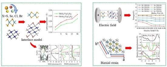
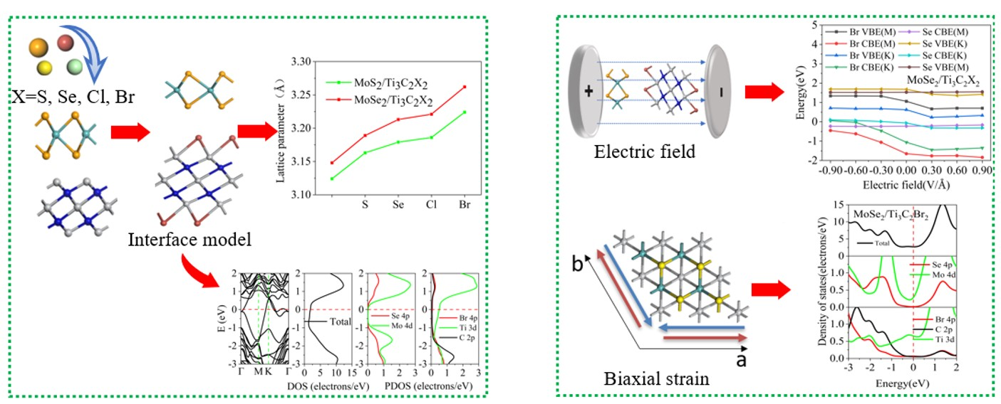
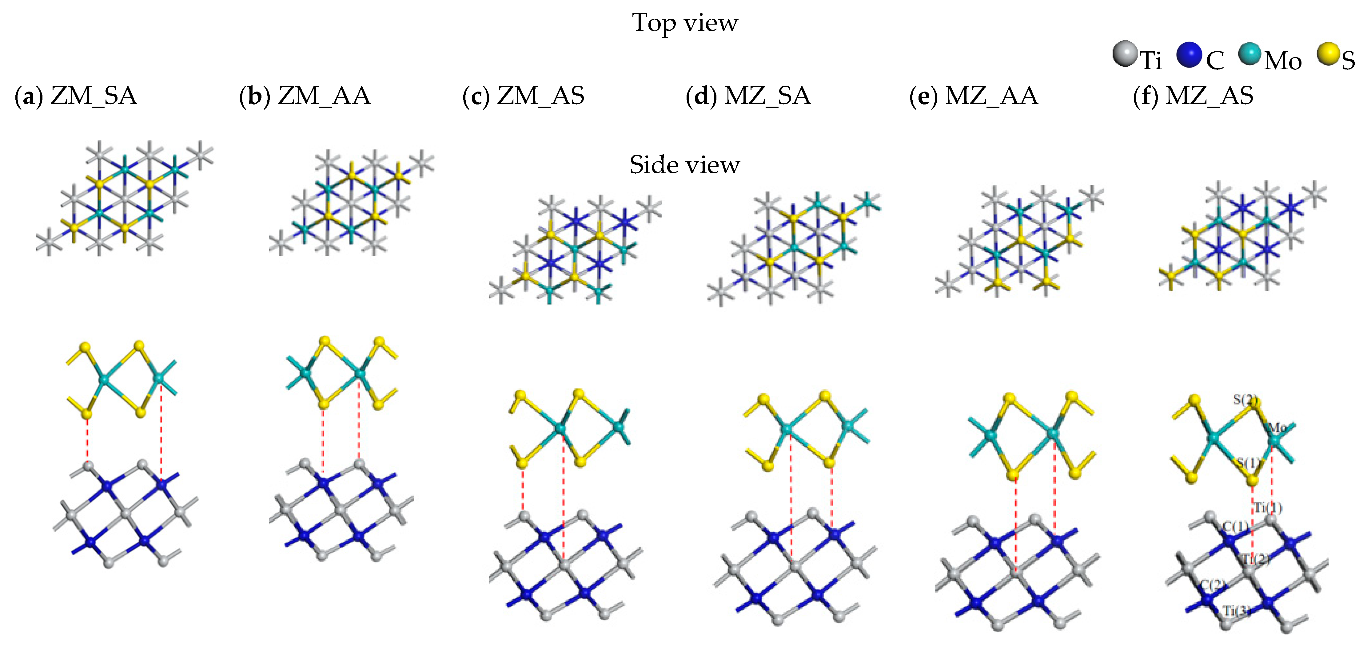
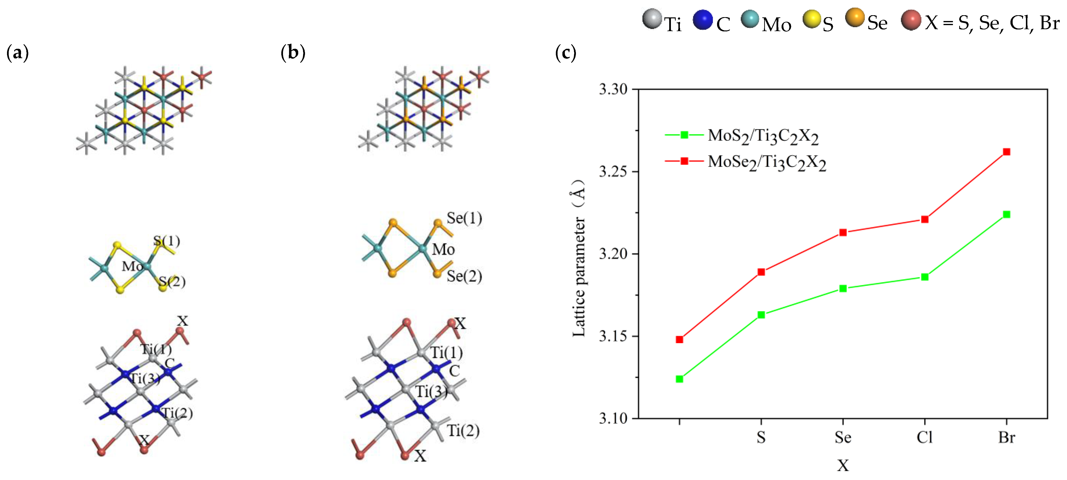
3.1. Structural Properties of the TMDs/Ti3C2 Heterostructures

The lattice constants of our optimized MoS2, MoSe2, and Ti3C2 monolayers were 3.15 Å, 3.24 Å and 3.12 Å, respectively, which were in good agreement with the previous studies [46,47]. They all have a hexagonal crystal structure with a space group of P63/mmc, and they possess a lattice mismatch rate within a reasonable range of less than 4%, allowing the construction of heterostructures [48]. According to the high-symmetry stacking mode, there are six possible TMDs/Ti3C2 configurations, taking MoS2/Ti3C2 heterostructures as an example, see Figure 1 (six high-symmetry MoSe2/Ti3C2 heterostructures, see Figure S1): (a) the ZM_SA Configuration: S and Mo atoms of MoS2 are on top of Ti and C atoms of Ti3C2, respectively; (b) the ZM_AA Configuration: S and Mo atoms of MoS2 are on top of C and Ti atoms of Ti3C2, respectively; (c) the ZM_AS Configuration: S and Mo atoms of MoS2 are on top of Ti atoms and hollow sites of Ti3C2, respectively; (d) the MZ_SA Configuration: S and Mo atoms of MoS2 are on top of C atoms and hollow sites of Ti3C2, respectively; (e) the MZ_AA Configuration: Mo and S atoms of MoS2 are on top of C atoms and hollow sites of Ti3C2, respectively; (f) the MZ_AS Configuration: Mo and S atoms of MoS2 are on top of Ti atoms and hollow sites of Ti3C2, respectively.
Table 1 lists our calculated binding energies, interlayer distance, and bond lengths for the six possible stacking configurations of MoS2/Ti3C2 heterostructures. It can be seen that the binding energies of these MoS2/Ti3C2 heterostructures were all negative, indicating that the formation of all the heterostructures was exothermic. A lower binding energy represents a more stable heterostructure structure. The ZM_SA configuration of MoS2/Ti3C2 had the lowest binding energy of −1.79 meV/Å, so it was energetically the most stable configuration among the six configurations. It is noted that the interlayer distance d of the MoS2/Ti3C2 heterostructure was very small (in the range of 1.68 Å to 2.47 Å), which indirectly indicated a strong interaction between the layers [49,50]. Table 2 presents the binding energy of −1.03 meV/Å for the most stable configuration SA_ZM of the MoSe2/Ti3C2 heterostructure, while the AS_ZM configuration had the maximum binding energy of −0.39 meV/Å. The binding energies of all six configurations were negative, indicating the stability of the MoSe2/Ti3C2 heterostructure. The interlayer distance d of the six configurations of MoSe2/Ti3C2 heterostructures ranged from 1.89 Å to 2.56 Å, which was similar to that of MoS2/Ti3C2 heterostructures.
A comparison of the data in Table 1 and Table 2 showed that the binding energies of all these MoS2/Ti3C2 heterostructures were smaller than those of the corresponding MoSe2/Ti3C2 heterostructures; meanwhile, MoS2/Ti3C2 had a smaller interlayer distance than the MoSe2/Ti3C2 heterostructures. These findings showed that the MoS2/Ti3C2 heterostructures are more stable. We calculated the Ti–C bond length in the original monolayer Ti3C2 as 2.057 Å. As shown in Table 1 and Table 2, the Ti(3)–C(2) bond length dTi(3)–C(2) showed almost no change, but the Ti(1)–C(1) bond lengths of the upper layer of Ti3C2 were stretched in the TMDs/Ti3C2 heterostructures. The reason for this may be that the charge transfer from Ti3C2 to TMDs leads to the stretching of the Ti(1)–C(1) bond. The Mo–S(1) minus Mo–S(2) value (d12) and Mo–Se(1) minus Mo–Se(2) value (d34) are also presented in Table 1 and Table 2. d12 ranged from 0.021 Å to 0.134 Å, and d34 ranged from 0.013 Å to 0.107 Å, indicating that the TMDs/Ti3C2 heterostructure slightly destabilizes the TMDs monolayer. Moreover, the d12 values in the MoS2/Ti3C2 heterostructure were all greater than the d34 in the MoSe2/Ti3C2 heterostructure, suggesting that the interlayer electron coupling effect of MoS2/Ti3C2 is greater than that of MoSe2/Ti3C2. This conclusion was consistent with the results of our calculated interlayer distance and binding energy. We also noted that the binding energy and interlayer distance of the ZM_SA configurations were the smallest, so the ZM_SA configuration is the most stable configuration among the 12 configurations of MoS2/Ti3C2 heterostructures and MoSe2/Ti3C2 heterostructures considered here.
We also further investigated the effects of novel functional groups (S, Se, Cl, Br) on the structural properties of TMDs/Ti3C2 heterostructures. Previous experimental studies [51] have shown that the Ti3C2X2 (X = S, Se, Cl, Br) are the most stable when the surface functional groups of Ti3C2 are located in the cavity centers of Ti atoms and aligned perpendicularly to the Ti atoms in the middle layer because of the site-blocked repulsion reaction between the C atoms and the surface functional groups. Therefore, in this work, when the surface of Ti3C2 was terminated by functional groups (S, Se, Cl, Br) in MoS2/Ti3C2X2 and MoSe2/Ti3C2X2 heterostructures, we focused on the case that the functional groups are located above the hole center of the Ti atom and perpendicular to the middle Ti atom, as shown in Figure 2a,b, respectively.
It can be clearly observed from Figure 2c that the lattice parameters of TMDs/Ti3C2X2 heterostructures changed significantly due to the addition of surface functional groups. The lattice parameter of the MoS2/Ti3C2 heterostructure was 3.124 Å. With the addition of each functional group, the lattice parameter obviously increased, and MoS2/Ti3C2Br2 had the maximum lattice parameter of 3.224 Å. The lattice parameter of MoS2/Ti3C2S2, MoS2/Ti3C2Se2 and MoS2/Ti3C2Cl2 increased to 3.163 Å, 3.179 Å and 3.186 Å, respectively. Similarly, the lattice parameters of the MoSe2/Ti3C2 heterostructure increased with the addition of functional groups. The lattice parameters of the MoSe2/Ti3C2 heterostructure were 3.148 Å, while MoSe2/Ti3C2S2, MoSe2/Ti3C2Se2, MoSe2/Ti3C2Cl2, and MoSe2/Ti3C2Br2 were 3.189 Å, 3.213 Å, 3.221 Å, and 3.262 Å, respectively. Therefore, the surface functional groups had a significant effect on the structural properties of MoS2/Ti3C2X2 and MoSe2/Ti3C2X2.
To further understand the stability of these TMDs/Ti3C2X2 heterostructures, we calculated the binding energy, interlayer distance, and structural parameters of TMDs/Ti3C2X2 (X = S, Se, Cl, Br) as shown in Table 3. We provide the coordinates of the TMDs/Ti3C2X2 (X = S, Se, Cl, Br) optimized structure in the Supplementary Materials, see Table S1. The binding energies of MoS2/Ti3C2X2 and MoSe2/Ti3C2X2 were negative. The MoSe2/Ti3C2Cl2 heterostructure possessed the highest binding energy (−3.12 meV/Å), while the MoS2/Ti3C2S2 heterostructure had the lowest binding energy (−8.44 meV/Å), indicating that the MoS2/Ti3C2S2 heterostructure was more stable. The interlayer distance of these heterostructures varied from 2.78 Å to 3.14 Å, which was significantly larger than that of the TMDs/Ti3C2 heterostructure, and a larger interlayer distance indicated a weaker electronic coupling between the monolayer TMDs and T3C2X2. It can be concluded that MoS2/Ti3C2X2 and MoSe2/Ti3C2X2 are typical van der Waals heterostructures.
It can also be seen from Table 3 that in MoS2/Ti3C2X2 and MoSe2/Ti3C2X2, the surface functional group of monolayer Ti3C2 caused an increase in the Ti–C bond length (dTi–C). Among them, the dTi–C of the MoSe2/Ti3C2S2 heterostructure reached 2.193 Å, an increase of 0.136 Å from the original 2.057 Å. The Ti–C bond length dTi–C of the MoS2/Ti3C2Cl2 heterostructure increased by 0.047 Å. The bond lengths between Ti(1) and X in the top layer of Ti3C2X2 were almost the same as those between Ti(2) and X in the bottom layer of Ti3C2X2, which means that the stacking of MoS2 and MoSe2 in these heterostructures hardly changes the spatial structure of Ti3C2X2. The strong coupling between the Ti3C2 and TMD interface was weakened by the functional group (S, Se, Cl, Br). The value of d56 was defined as Mo–Se(1) minus Mo–Se(2) or Mo–S(1) minus Mo–S(2) in TMDs/Ti3C2X2 (X = S, Se, Cl, Br). The MoS2/Ti3C2S2 heterostructure possessed the maximum d56 (0.009 Å), while d56 was zero in the MoSe2/Ti3C2Se2 heterostructure, indicating that the spatial structure and two-dimensional properties of the original MoSe2 were well preserved. The above results show that the addition of surface functional groups can seriously weaken the electronic coupling between the monolayer TMDs and Ti3C2.

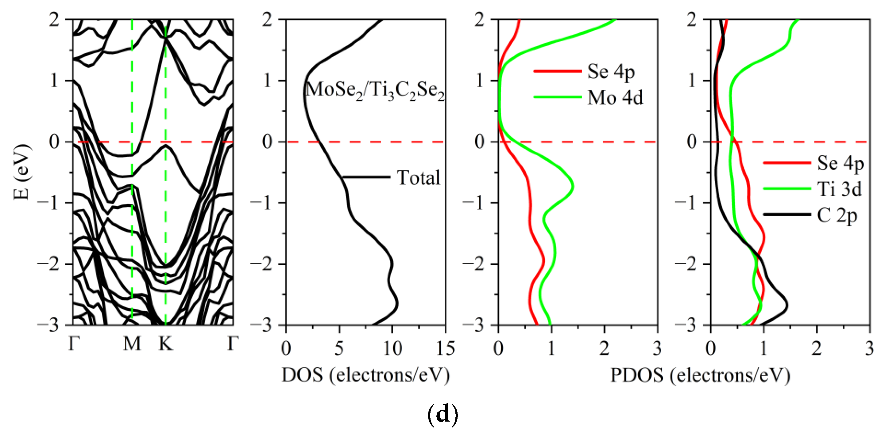
3.2. Electronic Properties of the TMDs/Ti3C2X2 Heterostructures

To investigate the electronic properties of the TMDs/Ti3C2 heterostructures, we choose the most stable configurations of ZM_SA and SA_ZM to further study the electronic properties of MoS2/Ti3C2X2 and MoSe2/Ti3C2X2, respectively. The energy band structures and density of states of the MoS2/Ti3C2 heterostructure are presented in Figure 3. The Fermi energy level is set at zero energy. From Figure 3a, it can be seen that some energy bands cross the Fermi energy level, indicating the metallic nature of the MoS2/Ti3C2 heterostructure. Because of a strongly coupled interaction between the MoS2 and Ti3C2 monolayer, the energy bands have been hybridized severely. The total and partial density of states of the MoS2/Ti3C2 heterostructure is shown in Figure 3b; it can be seen that the energy band near the Fermi level is mainly dominated by the 3d orbit of the Ti atom and the 4d orbit of the Mo atom. Remarkably, the electrons of the S 3p orbit in the conduction band are unusually more than that of the Ti 3p orbit. Therefore, the conduction band is mainly contributed by the Mo 4d, S 3p, and Ti 3d orbitals. The energy band structures and density of states of the MoSe2/Ti3C2 heterostructure are presented in Figure 4. We note that the energy band of the MoSe2/Ti3C2 heterostructure (see Figure 4a) has no obvious hybridization around the Fermi level, which is different from the MoS2/Ti3C2 heterostructure. Compared with MoS2/Ti3C2, MoSe2/Ti3C2 has more concentrated energy bands, leading to a decrease in conductivity. The total and partial density of states of the MoSe2/Ti3C2 heterostructure is shown in Figure 4b; we know that the energy bands near the Fermi energy level are dominated by Ti 3d and Mo 4d orbitals. The Ti 3p orbital and C 2p orbital make a slight contribution near the Fermi energy level. The conduction band is mainly formed by Ti 3d and Mo 4d orbitals, while the valence band is formed by C 2p, Ti 3d, and Mo 4d orbitals, and the C 2p orbital plays a dominant role in the MoSe2/Ti3C2 heterostructure. Finally, by comparing the density of states of MoS2/Ti3C2 with that of the MoSe2/Ti3C2 heterostructure, we find that the peak of Ti 3d and Mo 4d in the MoS2/Ti3C2 heterostructure moves towards a higher energy level.
It is well known that both MoS2 and MoSe2 are semiconductors in nature and exhibit a direct band gap at the K point in the Brillouin zone [52]. However, our calculations show that the S 3p orbitals, the Se 4p orbitals, and the Mo 4d orbitals in the TMDs/Ti3C2 heterostructure have a large number of electrons crossing the Fermi energy level, which is sufficient to indicate that Ti3C2 induces a significant change in the electronic properties of the TMDs monolayer.
To further understand the electronic properties, the Mulliken charge and bond populations of TMDs/Ti3C2 were calculated; see Tables S2 and S3. The interlayer electron coupling of the MoS2/Ti3C2 heterostructure is strong due to the overlap of electron clouds between MoS2 and Ti3C2 (the bond population of the S–Ti bond is 0.48 Å). The Ti3C2 in the MoS2/Ti3C2 heterostructure obtains 0.06 e from the upper MoS2 layer, and the Ti atom in Ti3C2 loses 1.55 e, and 1.50 e of Ti is transferred to the C atom. The bonding behavior of the MoS2/Ti3C2 heterostructure is covalent in nature, as indicated by the bond populations. For MoSe2/Ti3C2, the bond population of the Se–Ti bond has a large negative value (−0.83 Å), suggesting a weak van der Waals interaction between MoSe2 and Ti3C2. According to the positive and negative values of the bond population, we can conclude that the bonding behavior in the MoSe2/Ti3C2 heterostructure is a combination of covalent and ionic bonds.
The Mulliken charge analysis shows that more electrons are transferring from Ti3C2 to MoS2 in the MoS2/Ti3C2 heterostructure. We also noted that the Mo atom in MoSe2/Ti3C2 and MoS2/Ti3C2 obtains 0.35e and 0.01e, respectively. Moreover, the partial density of states in Figure 3b and Figure 4b shows that the density of the electrons of the Mo 4d orbital in the MoSe2/Ti3C2 heterostructure at the Fermi energy level is much higher than that in the MoS2/Ti3C2 heterostructure. As a result, the Mo 4d orbital in MoSe2/Ti3C2 obtains more electrons from other atoms than that in MoS2/Ti3C2.
The electronic properties of these heterostructures were affected by the surface termination atoms of Ti3C2, as illustrated in Figure 5 and Figure 6. Compared with MoS2/Ti3C2 and MoSe2/Ti3C2, the electronic properties of MoS2/Ti3C2X2 and MoSe2/Ti3C2X2 were obviously different. Although TMDs/Ti3C2X2 heterostructures still exhibited metallic behavior, the peak values of density of states (DOS) at the Fermi level were lower than those of TMDs/Ti3C2 heterostructures. Based on our calculated DOS, it is worth noting that MoS2 and MoSe2 retained the semiconductor nature in the TMDs/Ti3C2X2 heterostructures. This means that the presence of surface functional groups (Cl, Br, S, Se) weakened the interaction strength between TMDs and Ti3C2. Compared with the DOS of the original monolayer MoS2 and MoSe2, see Figures S2 and S3, that of MoS2 and MoSe2 in MoS2/Ti3C2Br2 and MoS2/Ti3C2Cl2 showed an upward shift of the Fermi energy level. From the partial density of states (PDOS) of MoS2/Ti3C2Br2 and MoS2/Ti3C2Cl2, it can be seen that the energy band near the Fermi level was mainly contributed to by the Ti 3d orbit. The Mo atom 4d orbital in MoS2/Ti3C2Br2 made a small charge contribution, while the Mo atom 4d orbital in MoS2/Ti3C2Cl2 made almost no charge contribution to the Fermi level. In addition, the atoms of the functional groups Cl and Br made almost no contribution near the Fermi level, as shown in Figure 5a,b. When the Ti3C2 surface was terminated by S and Se functional groups, the DOS of MoS2 and MoSe2 showed a downward shift of the Fermi level, while the S 3p and Se 4p orbitals made an obvious charge contribution near the Fermi level. The energy band near the Fermi level became flatter, and the effective mass of the electron was larger, so the conductivity decreased. It can be seen from the density of states of Ti3C2X2 (X = S, Se) that the S 3p and Se 4p orbital charges and Ti 3d orbital generated strong hybridization, respectively, as shown in Figure 5c,d. The metal behavior of the MoS2/Ti3C2X2 (X = Br, Cl, S, Se) heterostructure was mainly dominated by the Ti 3d orbital charge.
Figure 6a shows the energy band and density of states of the MoSe2/Ti3C2Br2 heterostructure. The bottom of the conduction band of MoSe2 moved downward and coincides with the Fermi level. At the Fermi energy level, only the Ti 3d orbital charge contributed. For MoSe2/Ti3C2Cl2 and MoSe2/Ti3C2S2, as shown in Figure 6b,c, the Fermi energy level was located between the top of the valence band and the bottom of the conduction band. The Ti 3d orbital dominated the metal properties of MoSe2/Ti3C2Cl2 and MoSe2/Ti3C2S2. For MoSe2/Ti3C2Se2, as shown in Figure 6d, the energy band structure of MoSe2 remained unchanged, and the Fermi level was located at the top of the valence band. The Se 4p and Ti 3d orbitals in Ti3C2Se2 generate strong hybridization, which dominated the conductivity of MoSe2/Ti3C2Se2. Moreover, the PDOS of MoSe2 and MoS2 showed that both S 3p orbitals in MoS2 and Se 4p orbitals in MoSe2 made no charge contribution at the Fermi energy level. When S and Se were used as the functional group terminal in Ti3C2, the S 3p and Se 4p orbital charges played a leading role in the Fermi energy level.

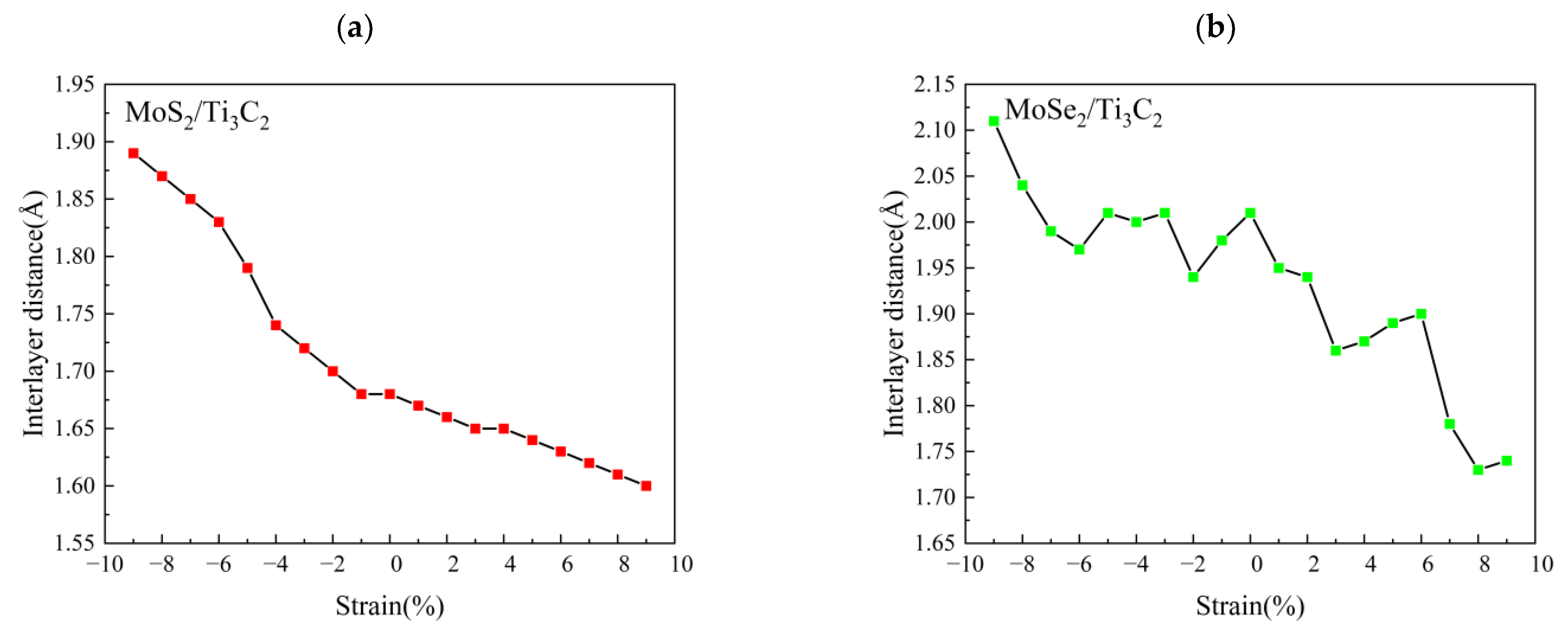
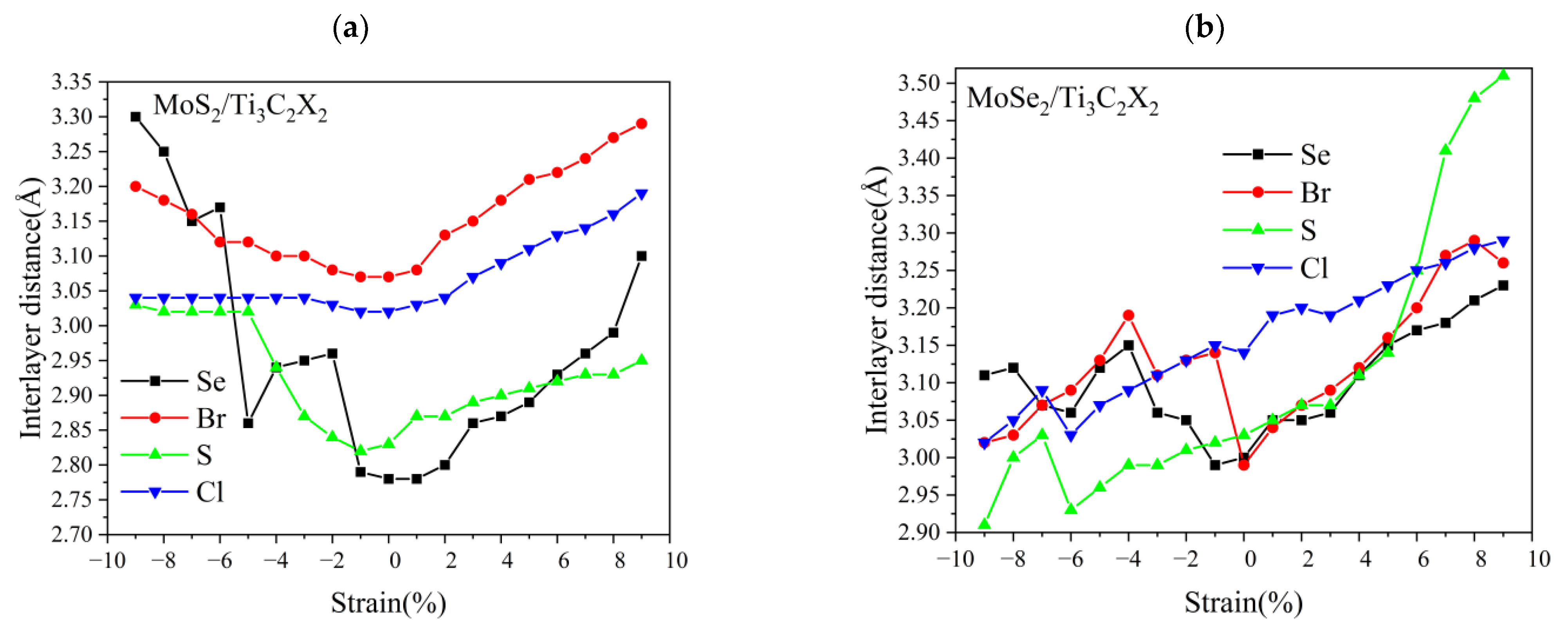
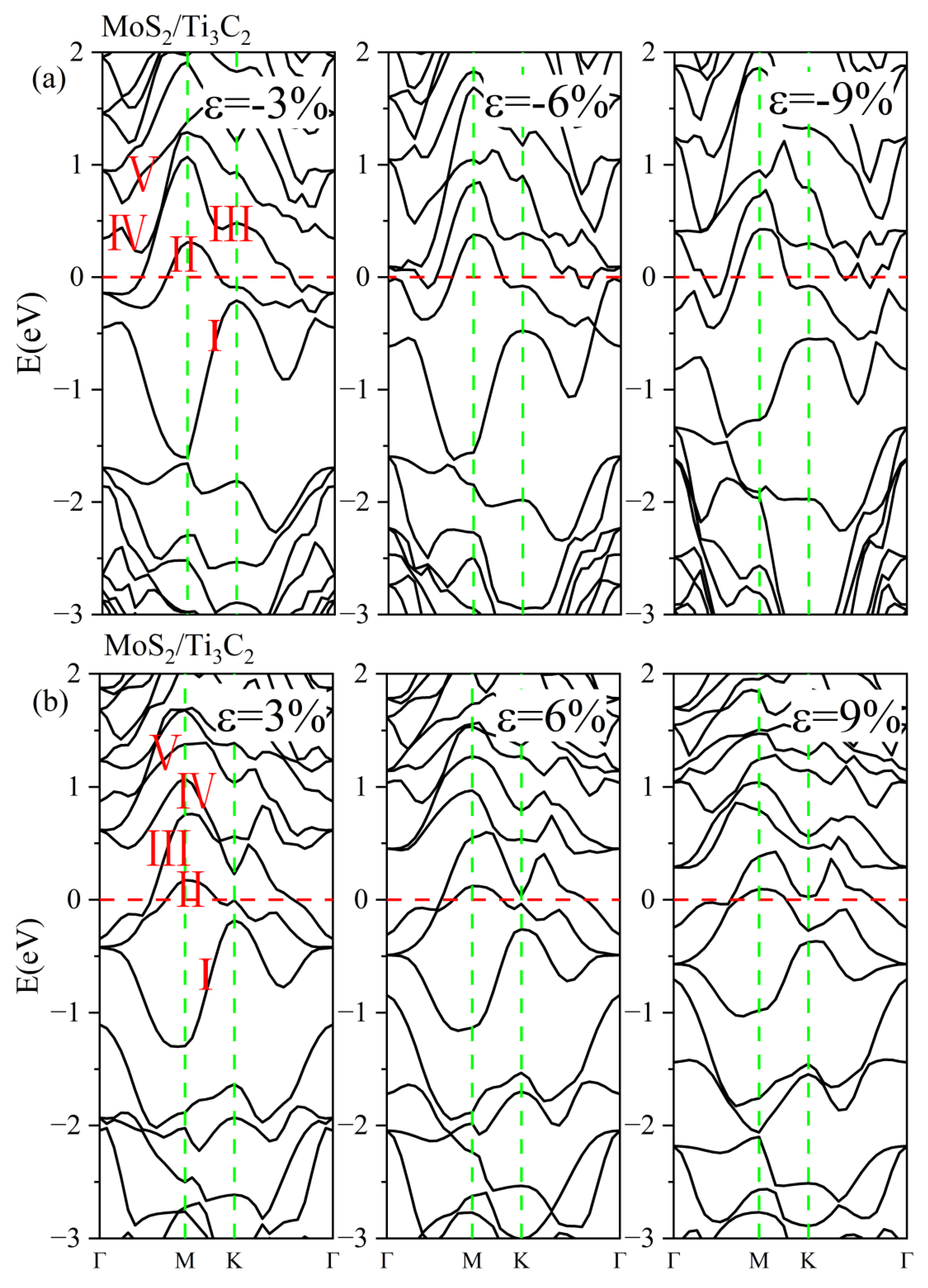
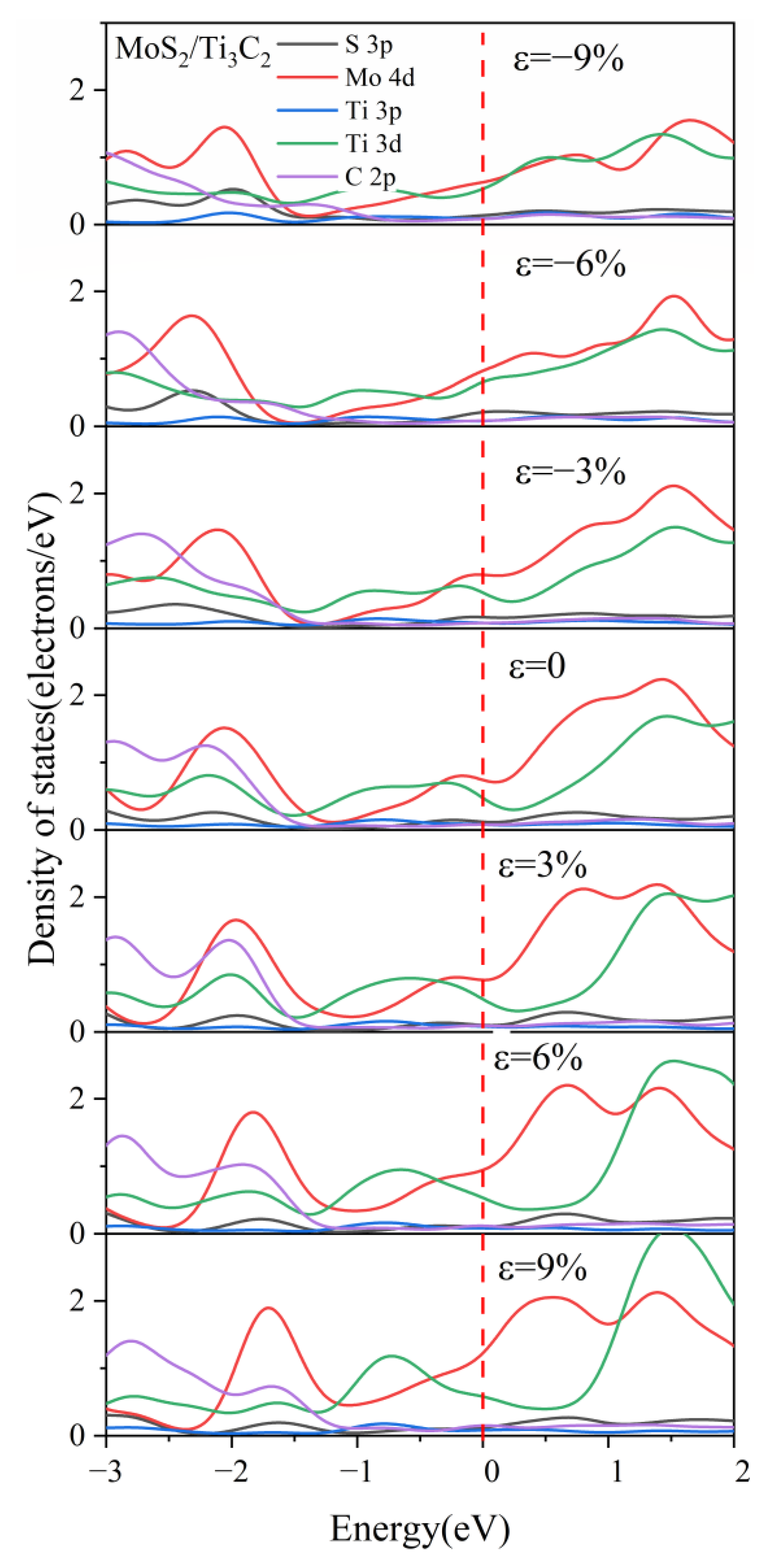
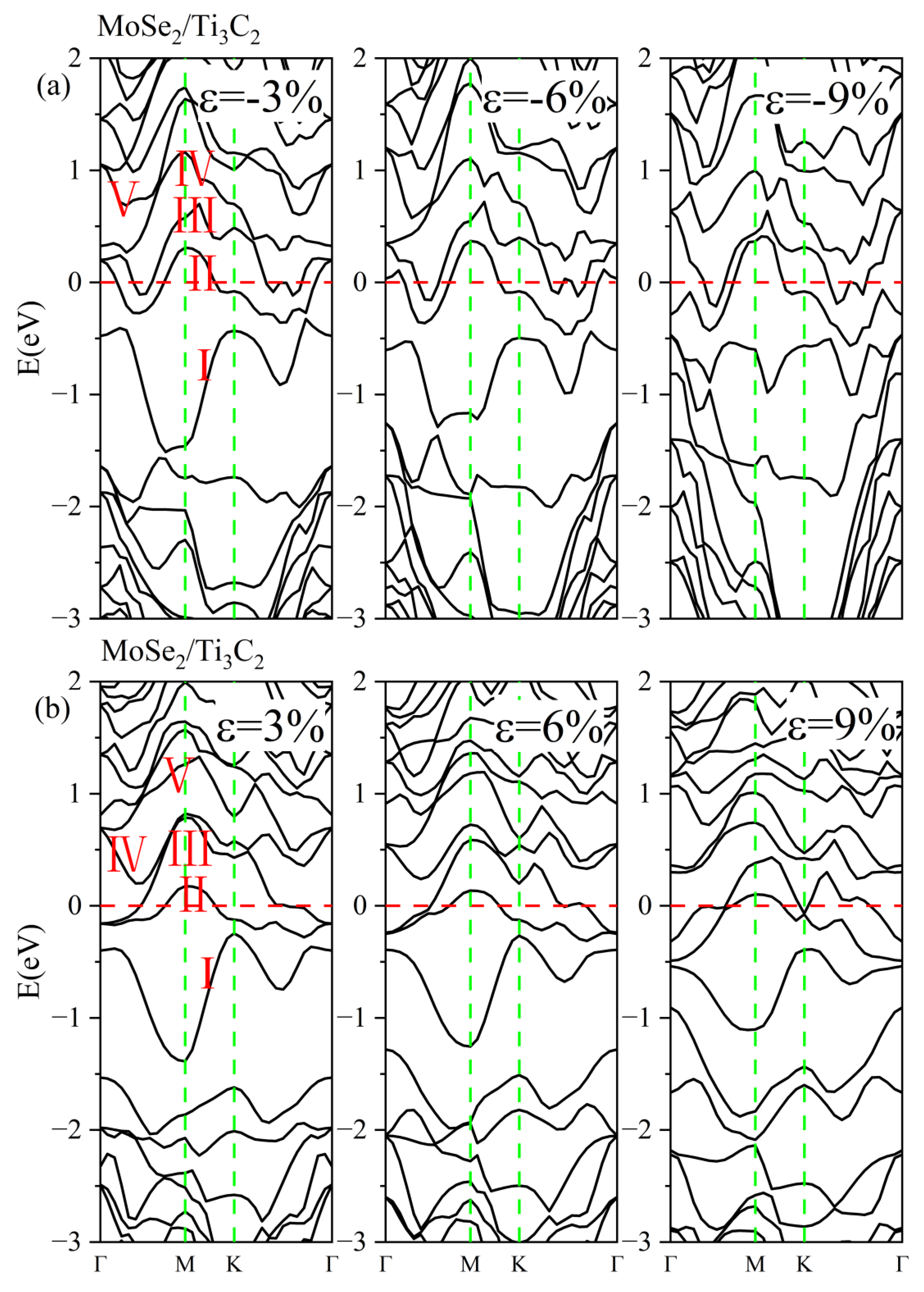
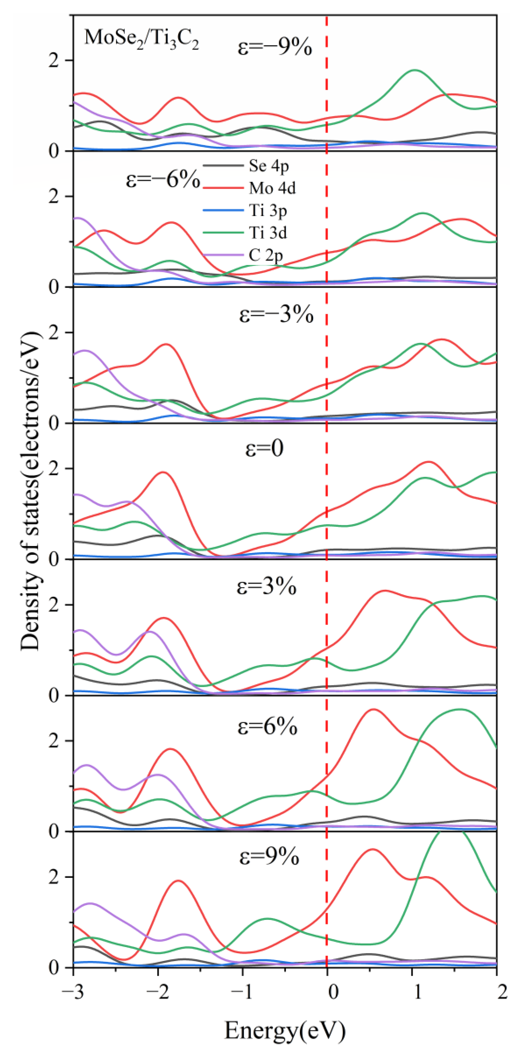
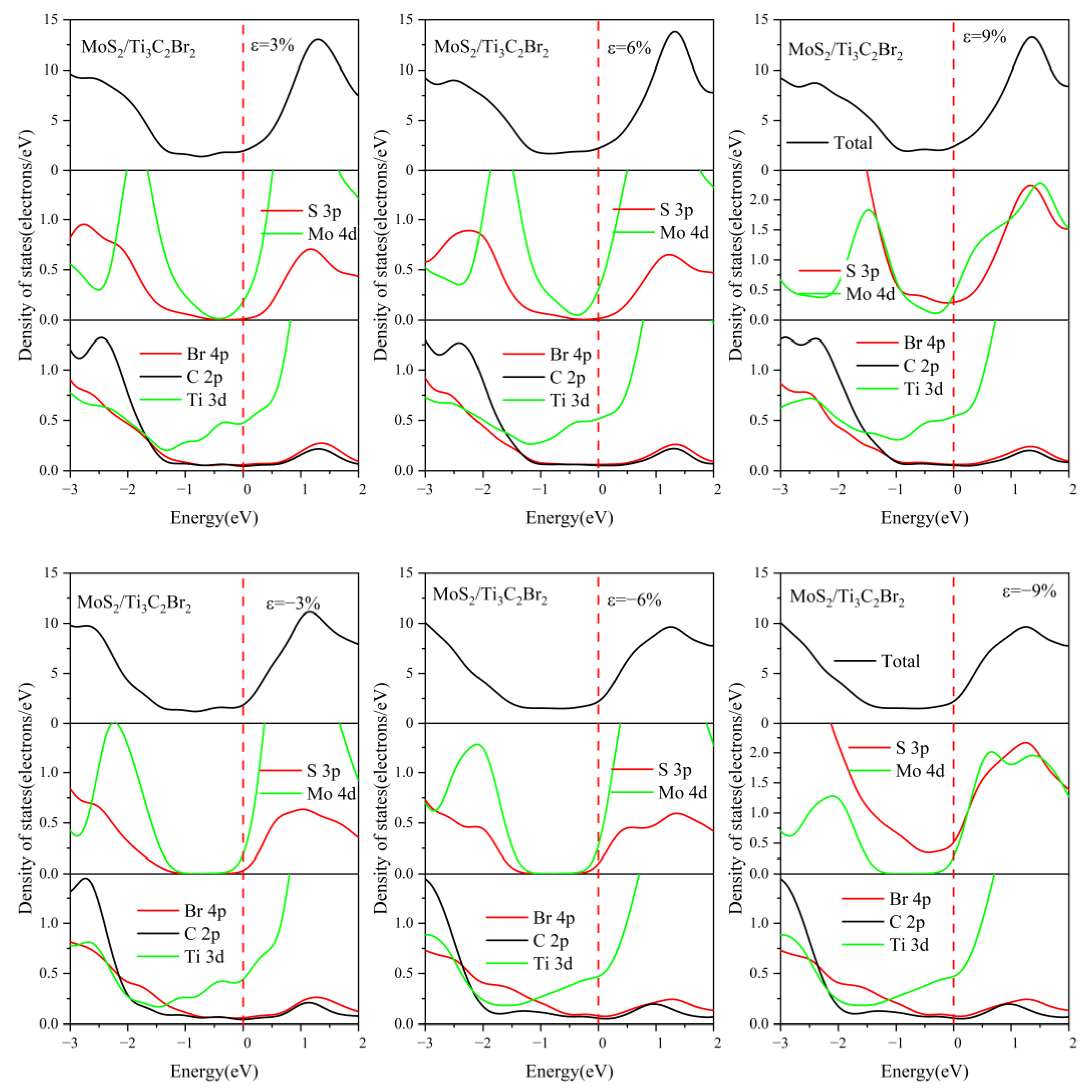
3.3. Effect of Biaxial Strain on the Structural and Electronic Properties of the TMDs/Ti3C2 Heterostructures

Strain can be used to tune the electronic properties of two-dimensional materials [53,54]. Here, we systematically investigated the effect of biaxial strain on the structural and electronic properties of TMDs/Ti3C2 and TMDs/Ti3C2X2. Considering a series of biaxial tensile or compressive strains ε in 0.01 steps from −9% to +9%, ε > 0 and ε < 0 represented the tensile and compressive strains, respectively. Figure 7a shows the variation curve of the MoS2/Ti3C2 interlayer distance with biaxial tensile (compressive) strain. It can be seen that the interlayer distance d of the MoS2/Ti3C2 heterostructure varies linearly with an increasing biaxial tensile or compressive strain. The interlayer distance of MoS2/Ti3C2 decreases to 1.56 Å when the biaxial tensile strain reaches 9%. Therefore, the biaxial tensile strain can enhance the electronic coupling strength between the monolayer MoS2 and Ti3C2. However, its interlayer distance gradually increases when subjected to biaxial compressive strain, and the interlayer distance increased to 1.89 Å at 9% compressive strain, indicating that the electron coupling strength between the monolayer MoS2 and Ti3C2 is severely weakened by the biaxial compressive strain. Figure 7b presents the variation curve of the MoSe2/Ti3C2 interlayer distance with the biaxial tensile (compressive) strain. The result is completely different to that of the MoS2/Ti3C2 heterostructure. The interlayer distance of the MoSe2/Ti3C2 heterostructure shows a fluctuating change with an increasing biaxial tensile or compressive strain. Based on the above Mulliken charge and bond populations analysis of MoS2/Ti3C2 and MoSe2/Ti3C2, it can be seen that the bond population of S–Ti in MoS2/Ti3C2 is positive, while that of Se–Ti in MoSe2/Ti3C2 is negative. Therefore, the reason may be that the MoSe2/Ti3C2 heterostructure has van der Waals interactions rather than strong electron coupling interactions.
We further investigated the effect of the biaxial tensile and compressive strain on the interlayer distance d of TMDs/Ti3C2X2 heterostructures; see Figure 8. It can be seen that under the condition of the applied strain, the interlayer distance of TMDs/Ti3C2X2 heterostructures presents a completely different behavior to that of MoS2/Ti3C2. The reason is the different electronic coupling strength between the monolayer TMDs and Ti3C2X2 due to the surface functional groups. The interlayer distance between MoS2 and Ti3C2Cl2 remains almost unchanged under the compressive strain, while it increases slightly with the increase in the tensile strain, as shown in Figure 8a. The interlayer distance of MoS2/Ti3C2S2 heterostructures presents a steady increase under tensile strain. When the compressive strain is in the range from 0 to 5%, its interlayer distance rapidly increases; when the compressive strain is above 5%, its interlayer distance is almost unchanged. For the MoS2/Ti3C2Br2 heterostructure, under the condition of compressive or tensile strain, the coupling strength between valence electrons of Br atoms and the 4d orbital of Mo atoms is weakened. As a result, the interlayer distance between MoS2 and Ti3C2Br2 increases slightly with the increase in the applied strain. Compared with MoS2/Ti3C2X2 (X = S, Br, Cl), the interlayer distance of MoS2/Ti3C2Se2 presents a significantly fluctuating change in the case of compressive strain. The reason may be that the Se atom induces the aberration of a crystal lattice due to its larger atomic radii [35]. When the compressive strain is applied, the lattice distortion becomes more pronounced, resulting in the fluctuation of the interlayer distance. For MoSe2/Ti3C2X2 (X = S, Se, Cl, Br), we also observed a similar trend under the condition of compressive strain; see Figure 8b. Therefore, we concluded that the fluctuation in the interlayer distance in MoS2/Ti3C2X2 (X = Se) and MoSe2/Ti3C2X2 is mainly attributed to the existence of the Se atom, and the displacement of the Se atom affects the structural stability of these heterostructures.
Figure 8b shows that the interlayer distance of MoSe2/Ti3C2X2 dramatically increases with the increase in the tensile strain, and the interlayer distances of MoSe2/Ti3C2Se2 and MoSe2/Ti3C2Br2 at 9% tensile strain increase to 3.23 Å and 3.26 Å, respectively. Under the compressive strain, their interlayer distance increases nonlinearly. Therefore, the applied strain weakened the interlayer interaction between MoSe2 and Ti3C2X2 (X = Se, Br). For MoSe2/Ti3C2S2 and MoSe2/Ti3C2Cl2, their interlayer distance presents the same trend under the applied strain. Under the tensile strain, the interlayer distance increases, while under the compressive strain, the interlayer distance becomes increasingly smaller. Moreover, the interlayer distance of MoSe2/Ti3C2S2 is more sensitive to the applied strain than that of MoSe2/Ti3C2Cl2. It is noted that the interlayer distance of MoSe2/Ti3C2S2 increased to 3.52 Å at 9% tensile strain, in contrast; its interlayer distance decreased to 2.91 Å at 9% compressive strain.
To explore the effect of biaxial strain on the electronic properties of TMDs/Ti3C2 heterostructures, we first investigated the Mulliken charge of TMD/Ti3C2 heterostructure under tensile and compressive strain. Table 4 shows the Mulliken charge population of MoS2/Ti3C2 heterostructures, at free strain, Ti3C2 loses 0.07e, which is transferred to the monolayer MoS2. At a tensile strain of 9%, Ti3C2 loses more electrons (0.11e). Moreover, Mo atoms also lose 0.05 electrons when subjected to tensile strain. At a compressive strain of 9%, Ti3C2 loses fewer electrons (0.03e). Table 5 shows the Mulliken charge population of MoSe2/Ti3C2 heterostructures. At a compressive strain of 9%, MoSe2 loses more electrons (0.08e), which are transferred to Ti3C2. These results showed that the interlayer electron transfer in both MoS2/Ti3C2 and MoSe2/Ti3C2 can be well regulated by biaxial strain. The difference is that in the MoS2/Ti3C2 heterostructure the electrons are transferred from Ti3C2 to MoS2, while in the MoSe2/Ti3C2 heterostructure, the electrons are transferred from MoSe2 to Ti3C2. Moreover, in the MoS2/Ti3C2 heterostructure the transferring electrons increase with increasing tensile strain, while in the MoSe2/Ti3C2 heterostructure, they increase with increasing compressive strain.
To further investigate the effect of biaxial strain on the electronic properties of TMDs/Ti3C2 heterostructures, we calculated their energy band structures and density of states under different strains. Figure 9a presents the energy band structures of MoS2/Ti3C2 heterostructures under compressive strain. As the compressive strain increased, the valence band I moved down and away from the Fermi energy level, and it became flatter and flatter. The energy bands II and III at the Γ point were split, and the energy band II became more dispersed. Moreover, the energy bands III and IV were combined, and then they moved away from the Fermi energy level with increasing compressive strain. Figure 9b shows the energy band structures of MoS2/Ti3C2 heterostructures under tensile strain. It can be seen that the increase in the tensile strain caused the valence bands I, II, and III to move away from the Fermi energy level and become flatter. Moreover, the conduction bands IV and V moved toward the Fermi energy level, and they showed more hybridization, resulting in an increase in the conductivity of the MoS2/Ti3C2 heterostructure [55].
Figure 10 shows the DOS of the MoS2/Ti3C2 heterostructure under different biaxial strains. It was obvious that the Fermi energy level was dominated by Mo 4d and Ti 3d orbitals. Moreover, the contribution of the Mo 4d orbital to the conduction band lessened with increasing compressive strain, while the contribution of Mo 4d and Ti 3d orbitals to the valence band increased with the increasing tensile strain. It can also be seen that the peak value of Ti atoms in the range of the conduction band increased with increasing tensile strain, while the peak value of Mo atoms remained almost unchanged with increasing tensile strain. The peak value of Mo atoms in the range of the valence band increased with the tensile strain and moved toward the Fermi energy level. Based on our calculated DOS of the MoS2/Ti3C2 heterostructure, the interlayer interaction between the monolayer MoS2 and Ti3C2 presented different behavior under tensile and compressive strain, and the interaction strength was strengthened under tensile strain, but weakened under compressive strain.
Figure 11a gives the energy band structures of the MoSe2/Ti3C2 heterostructure under different compressive strains. With increasing compressive strain, the conduction bands III and IV gradually merged at the Γ point and moved away from the Fermi level. The valence band I become flatter, while the valence band II crossing the Fermi level became more tortuous, indicating a decrease in conductivity. Figure 11b displays the energy band structures of the MoSe2/Ti3C2 heterostructure under different tensile strains. As the tensile strain increased, the energy bands II and III were split at the Γ point, and the energy bands IV and V showed more hybridization. Moreover, the energy bands crossing the Fermi energy level became more dispersed under tensile strain, inducing an increase in conductivity. We also noted that the pseudogap of the MoSe2/Ti3C2 heterostructure disappeared with increasing compressive or tensile strain. Therefore, the applied strain can effectively tune the electronic properties of the TMDs/Ti3C2 heterostructures.
Figure 12 illustrates the DOS of the MoSe2/Ti3C2 heterostructure with different biaxial strains. The peak value of Mo 4d orbitals at −1.8 eV gradually decreased under compressive strain, while the peak value of Ti 3d orbitals at 0.9 eV increased with increasing compressive strain. Under tensile strain, the peak value of both the Ti 3d orbital at 0.9 eV and the Mo 4d orbital at 1.2 eV increased with increasing tensile strain. Moreover, the peak value of Ti 3d orbitals moved away from the Fermi level, while in contrast, the peak value of the Mo 4d orbitals moved toward the Fermi energy level. It can be inferred from the variation of the DOS of MoSe2/Ti3C2 heterostructure with the strain that tensile strain increases the interlayer interaction, while compressive strain weakens the interlayer interaction. This result was consistent with the MoS2/Ti3C2 heterostructure.
We also investigated the DOS of MoS2/Ti3C2X2 under different biaxial strains, as shown in Figure 13, Figure 14, Figures S5 and S6. Compared with MoS2/Ti3C2Se2 and MoS2/Ti3C2Br2, the external strain had a slight effect on the DOS of MoS2/Ti3C2Cl2 and MoS2/Ti3C2S2, see Figures S5 and S6. The monolayer MoS2 remained in its band gap when a compressive strain was applied, while its band gap gradually disappeared with increasing tensile strain. This indicated that the tensile strain can improve the interaction strength between the monolayer MoS2 and Ti3C2Cl2 (or Ti3C2S2). For MoS2/Ti3C2Se2 and MoS2/Ti3C2Br2, the tensile strain induced the Mo 4d orbital to cross the Fermi level, indicating that the semiconductor nature of the monolayer MoS2 was completely destroyed. This means more electrons were transferred from the monolayer Ti3C2Br2 (or Ti3C2Se2) to MoS2. We also noted that the S 3p orbital in MoS2/Ti3C2Br2 obviously crossed the Fermi level when the compressive strain reached 9%. In contrast, compressive strain cannot result in the S 3p and Mo 4d orbitals crossing the Fermi level in MoS2/Ti3C2Se2, suggesting that MoS2 can preserve its band gap under compressive strain, while the position of its conduction band minimum (CBM) and valence band maximum (VBM) will be obviously shifted.
For comparison, the DOS of MoSe2/Ti3C2X2 under different biaxial strains was also investigated, see Figure 15, Figure 16, Figures S7 and S8. For these four kinds of MoSe2/Ti3C2X2 heterostructures, the band gap of monolayer MoSe2 disappeared with increasing compressive or tensile strain, and the Mo 4d orbitals and Se 4p orbitals passed through the Fermi energy levels. Therefore, the MoSe2/Ti3C2X2 heterostructure is more sensitive to external strain than the MoS2/Ti3C2X2 heterostructure. Moreover, these MoSe2/Ti3C2X2 heterostructures had a similar response to external strain. When there was no strain, the single-layer MoSe2 maintained its original semiconductor properties (see Figure 6), and the Fermi energy level was at the VBM of the MoSe2. When the tensile or compressive strain was above 6%, MoSe2 was transformed into a conductor. The tensile and compressive strain can obviously increase the charge contribution of Mo 4d orbitals and Se 4p orbitals at the Fermi energy level. Moreover, under compressive strain, the PDOS peak value of these MoSe2/Ti3C2X2 heterostructures becomes sharper, indicating that the electron localization is strong.

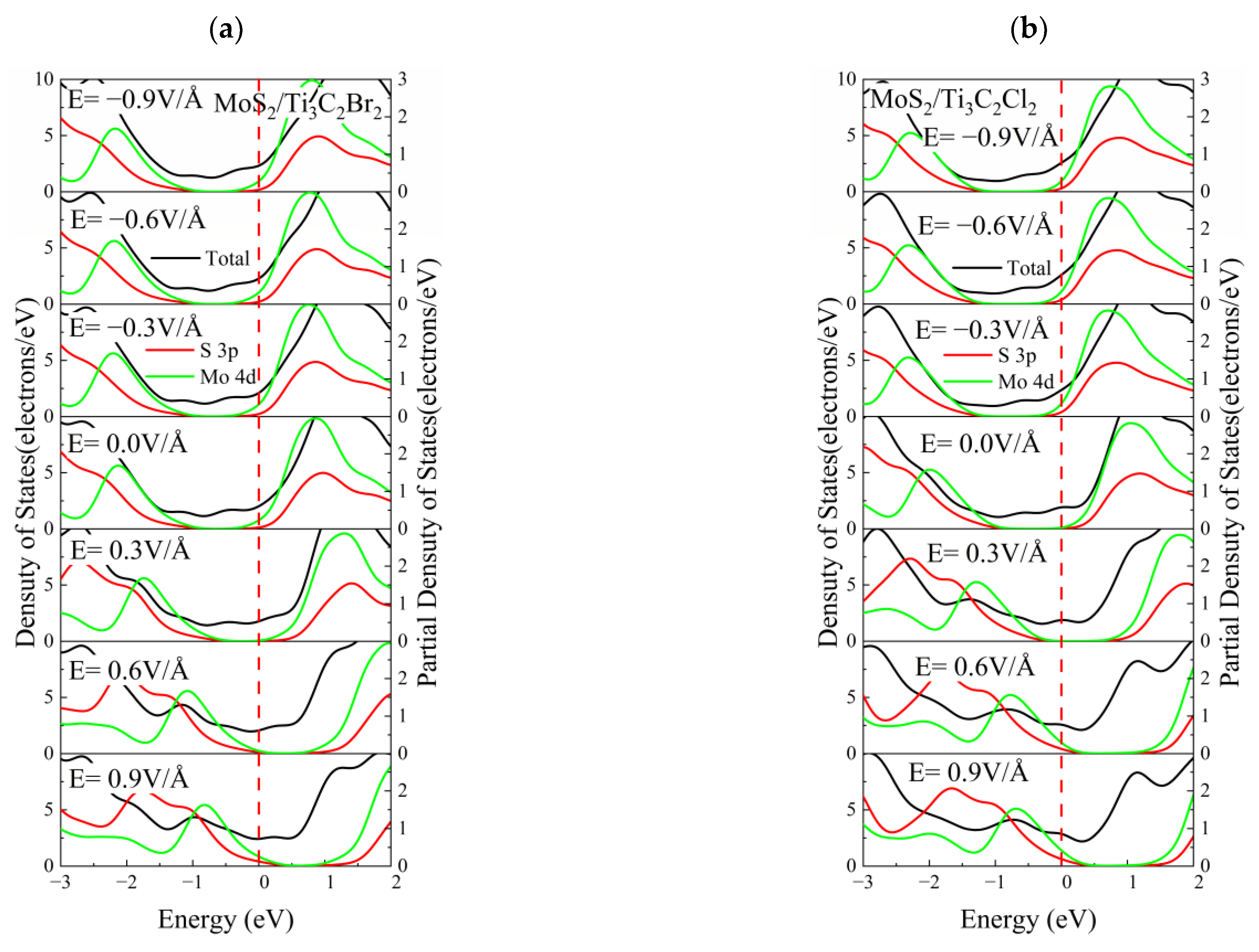
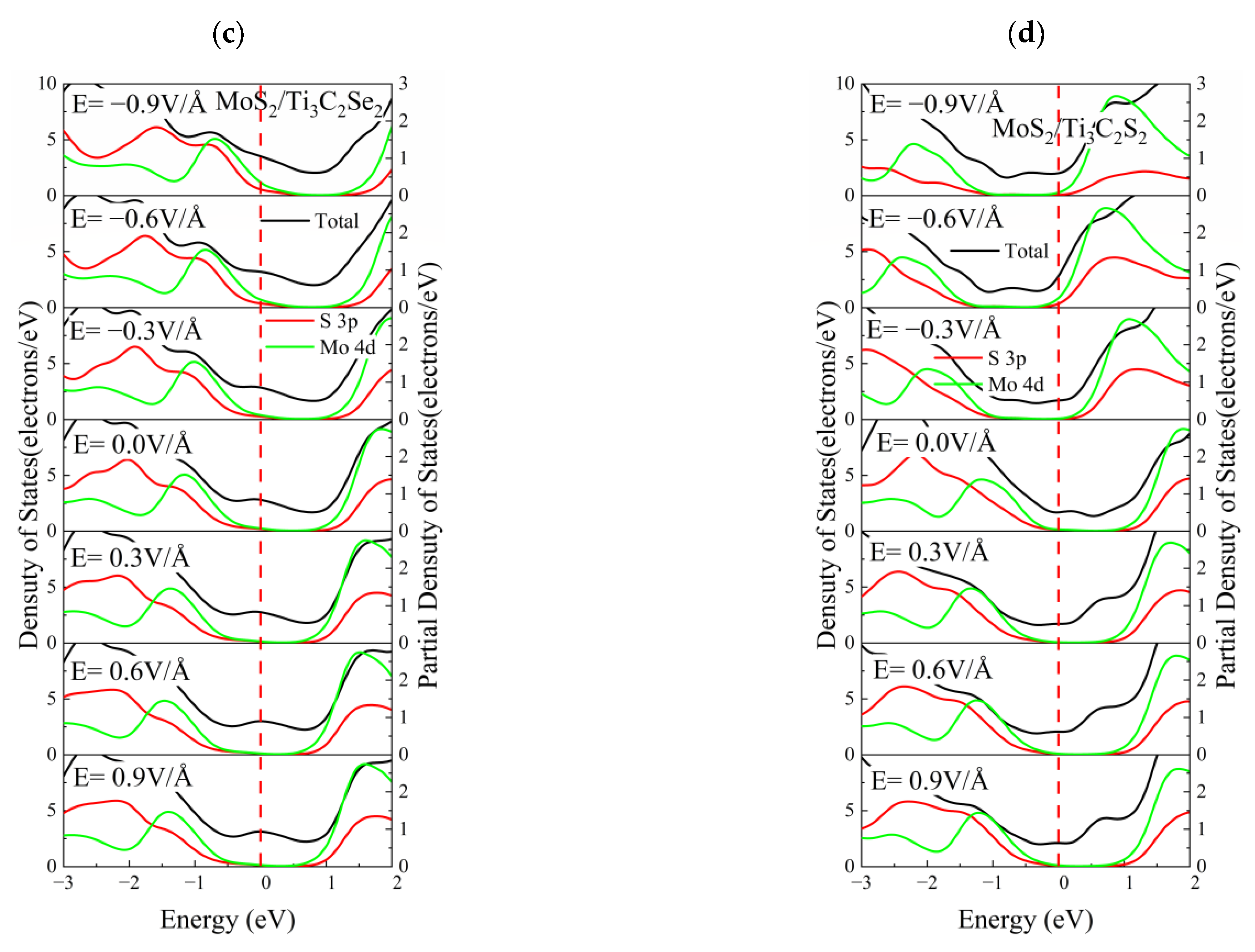
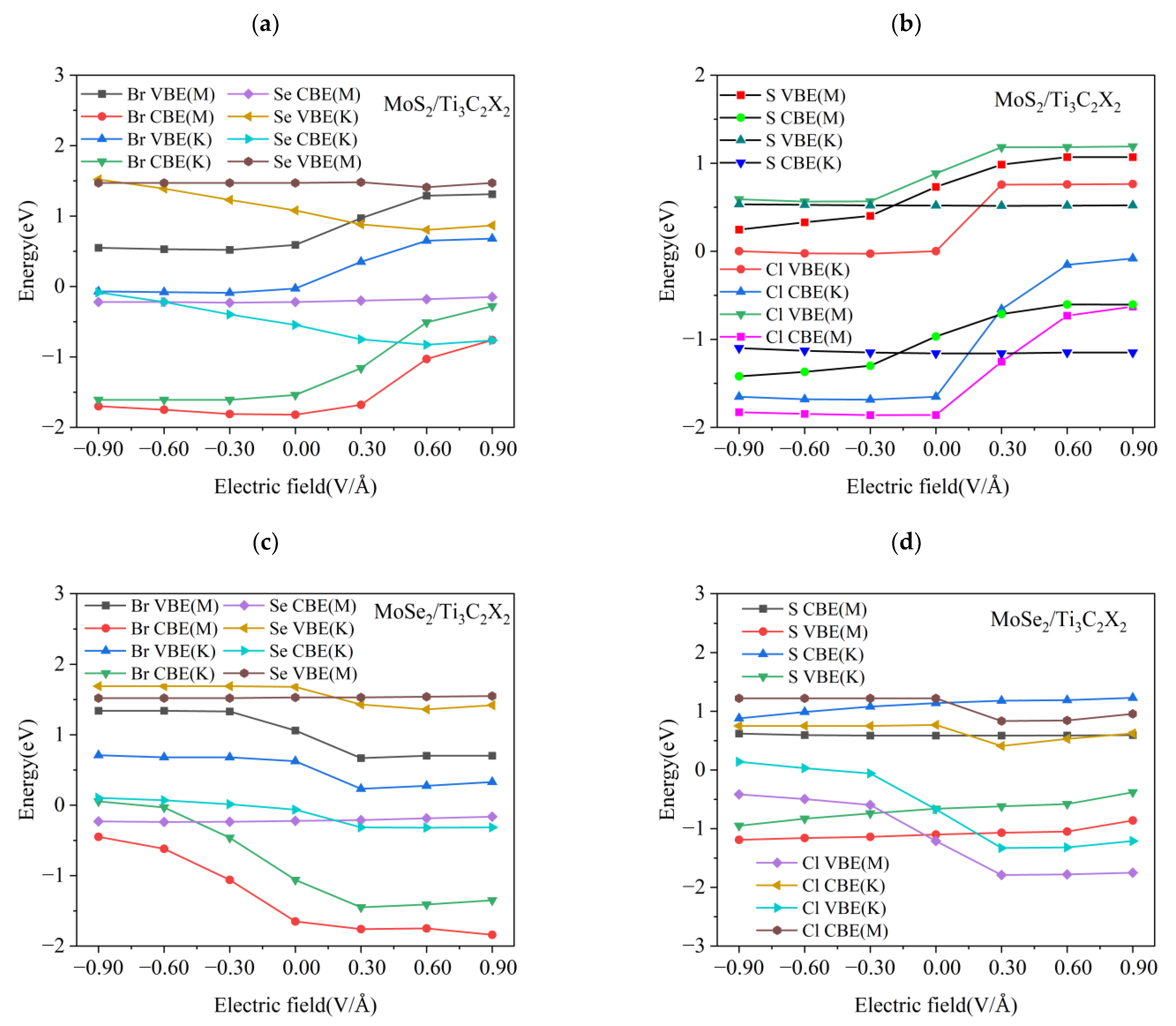
3.4. Effect of Electric Field on the Electronic Properties of the TMDs/Ti3C2X2 Heterostructures

Some studies [56,57] have shown that the electric field is a useful way to tune the electronic properties of heterostructures. In this section, we focus on the effects of the vertical electric field on the electronic properties of TMDs/Ti3C2X2 heterostructures. To determine the effect of different directions of the applied electric field on the electronic properties of these heterostructures, we defined that the direction of the TMDs pointing to Ti3C2X2 was the positive direction of the applied vertical electric field, and the reverse direction was negative. The gradient from −0.9 V/Å to +0.9 V/Å for the applied electric field was taken in steps of 0.3 V/Å.
Figure 17 shows the DOS of MoS2/Ti3C2X2 and PDOS of MoS2 in MoS2/Ti3C2X2 (X = S, Se, Cl, Br) under different electric fields. The monolayer MoS2 maintained its band gap under the positive and negative electric fields. The position of the valence band maximum (VBM) and conduction band minimum (CBM) of MoS2 in MoS2/Ti3C2Br2 and MoS2/Ti3C2Cl2 remained almost unchanged under the negative electric field. In contrast, the VBM and CBM of MoS2 in MoS2/Ti3C2Br2 and MoS2/Ti3C2Cl2 underwent a significant shift under the positive electric field, and the peak of the Mo 4d orbital moved toward a higher energy level, as shown in Figure 17a,b. Compared with MoS2/Ti3C2Br2 and MoS2/Ti3C2Cl2, the effect of the electric field on the VBM and CBM of MoS2 in MoS2/Ti3C2Se2 and MoS2/Ti3C2S2 presented a completely reverse case. The position of VBM and CBM of MoS2 in MoS2/Ti3C2Se2 and MoS2/Ti3C2S2 remained almost unchanged under the positive electric field, while obviously moving under the negative electric field. Moreover, the peak position of the Mo 4d orbital remained almost constant, see Figure 17c,d. The DOS values of MoSe2 in MoSe2/Ti3C2X2 (X = S, Se, Cl, Br) under different electric fields were investigated, and the results were very similar to the MoS2/Ti3C2X2, see Figure S4. Compared with MoS2/Ti3C2Br2 and MoS2/Ti3C2Se2, the total DOS of MoS2/Ti3C2S2 and MoS2/Ti3C2Cl2 obviously moved near the Fermi Level, suggesting the shift of VBE and CBE of MoS2. Moreover, under the condition of a positive electric field, the total DOS of MoS2/Ti3C2Cl2 presented a sharp peak around 1 eV.
We further analyzed the energy band structure of TMDs/Ti3C2X2 (X = S, Se, Cl, Br) heterostructures near the Fermi energy level in the electric field range from −0.9 V/Å to 0.9 V/Å, as shown in Figure 18. Figure 18a gives the variation patterns of the energy band edges at the M and K points near the Fermi energy level for MoS2/Ti3C2X2 (X = Se, Br) heterostructures under different electric fields. For MoS2/Ti3C2Br2, the conduction band edge (CBE) and valence band edge (VBE) at both the M the K points moved towards a higher energy level with increasing electric field strength in the positive direction, while they were almost pinned under the negative electric field. In contrast, both the CBE and the VBE of MoS2/Ti3C2Se2 at the K point moved towards a higher energy level with increasing negative electric field strength, while the CBE at the K point under the positive electric field moved towards a lower energy level. Under the positive electric field, both the CBE and VBE of MoS2/Ti3C2Se2 at the M point remained unchanged. For MoS2/Ti3C2X2 (X = S, Cl), see Figure 18b, the VBE and CBE of MoS2/Ti3C2Cl2 at the M point and K point near the Fermi level were similar to those of the MoS2/Ti3C2Br2 heterostructure. The energy level of both the CBE and VBE of MoS2/Ti3C2S2 at the M point increased linearly with increasing positive electric field strength, while it decreased slightly with the negative electric field. It is worth noting that the CBE and VBE of MoS2/Ti3C2S2 at the K point were almost pinned under the positive and negative electric fields. For MoSe2/Ti3C2Br2, the energy level of the CBE and VBE at the M and K points decreased linearly with an increasing positive electric field, while it increased with an increasing negative electric field, see Figure 18c. The energy band edge of MoSe2/Ti3C2Se2 was almost independent of the positive and negative electric fields. From Figure 18d, we know that for MoSe2/Ti3C2S2 the energy level of the CBE and VBE at the K point and M point were insensitive to the external electric field. For MoSe2/Ti3C2Cl2, the energy level of the CBE at the K point and M point showed a slight change under the condition of the positive electric field, while it could be pinned when the negative electric field was applied. The energy level of the VBE at the K point and M point remained unchanged when the electric field strength was increased to 0.3 V/Å. The energy band edges of TMDs/Ti3C2X2 (X = S, Se, Cl, Br) heterostructures showed a significant change near the Fermi energy level under different directional electric fields, indicating that the combined functional group with the electric field can effectively tune the related properties of TMDs/Ti3C2X2 (X = S, Se, Cl, Br) heterostructures.

4. Conclusions

The effects of biaxial strain and functional groups as well as electric fields on the structural and electronic properties of TMDs/Ti3C2 heterostructures were systematically investigated based on the density functional theory method. The six possible configurations of MoS2/Ti3C2 and MoSe2/Ti3C2 heterostructure stacks were first designed, and then geometrically optimized. ZM_SA were identified as the most energetically stable structural types of MoS2/Ti3C2 heterostructures with a binding energy of −1.79 meV/Å2. The most energetically stable structure type of MoSe2/Ti3C2 heterostructures was SA_ZM, its binding energy of −1.03 meV/Å2. The surface functional groups (S, Se, Cl, Br) of the monolayer Ti3C2 resulted in the lattice expansion of TMDs/Ti3C2X2 heterostructures, and the MoSe2/Ti3C2Br2 heterostructure possessed the maximum lattice parameters (3.262 Å). The conductivity of MoS2/Ti3C2 and MoSe2/Ti3C2 can be enhanced by increasing the biaxial tensile strain. When the surface of the monolayer Ti3C2 was occupied by S, Se, Cl, or Br, the coupling strength between the monolayer TMDs and Ti3C2 was obviously weakened, while the biaxial strain effectively improved their interaction strength. The different surface functional groups induced a different response of the electronic properties of TMDs/Ti3C2X2 heterostructures to the external electric field. The energy bands around the Fermi energy level of TMDs/Ti3C2X2 heterostructures obviously changed under the combined effect of surface functional groups with an electric field. These results demonstrated that TMDs/Ti3C2X2 (X = S, Se, Cl, Br) heterostructures possess rich electronic properties. Moreover, both MoS2/Ti3C2X2 (X = Se, Br) and MoSe2/Ti3C2X2 (X = S, Se, Cl, Br) are rather sensitive to an external strain field, while only TMDs/Ti3C2X2 (X = Cl, Br) strongly depends on an external positive electric field. We hope that these studies can provide a theoretical foundation for the application of TMDs/MXenes heterostructures in the field of high-performance nanoelectronic devices.

Supplementary Materials

The following supporting information can be downloaded at: https://www.mdpi.com/article/10.3390/nano13071218/s1, Figure S1: A schematic diagram of top and side views of MoSe2/Ti3C2 heterostructures for different stackings; Figure S2: Band structures and densities of states of the MoS2; Figure S3: Band structures and densities of states of the MoSe2; Figure S4: The DOS of MoSe2/Ti3C2X2 and PDOS of MoSe2 in MoSe2/Ti3C2X2 heterostructures under different electric fields. (a) X-Br, (b) X-Cl, (c) X-Se and (d) X-S; Figure S5: Density of states of the MoS2/Ti3C2Cl2 heterostructure with different biaxial strains; Figure S6: Density of states of the MoS2/Ti3C2S2 heterostructure with different biaxial strains; Figure S7: Density of states of the MoSe2/Ti3C2Cl2 heterostructure with different biaxial strains; Figure S8: Density of states of the MoSe2/Ti3C2S2 heterostructure with different biaxial strains; Table S1: Optimized structural parameters for the TMDs/Ti3C2X2 (X = S, Se, Br, Cl) heterostructure; Table S2: Mulliken charge (electron), bond length (Å) and bond populations of MoS2/Ti3C2; Table S3: Mulliken charge (electron), bond length (Å) and bond populations of MoSe2/Ti3C2.

Author Contributions

S.Z.: Data curation, Formal analysis, Investigation, Methodology, Resources, Software, Validation, Visualization, Roles/Writing—original draft, Writing-review & editing. C.L.: Conceptualization, Investigation, Methodology, Funding acquisition, Project administration, Supervision, Validation, Writing—review & editing. C.W.: Investigation, Visualization. D.M.: Investigation, Visualization. B.W.: Investigation, Visualization. All authors have read and agreed to the published version of the manuscript.

Funding

This research was funded by the National Natural Science Foundation of China (12172097) and the Natural Science Foundation of Heilongjiang Province, China (LH2021A006). And The APC was funded by the National Natural Science Foundation of China (12172097).

Data Availability Statement

Data are available on request from the corresponding author.

Conflicts of Interest

The authors declare that there is no conflict of interest regarding publication of this manuscript.

References

  1. Chen, H.L.; Han, J.N.; Deng, X.Q.; Fan, Z.Q.; Sun, L.; Zhang, Z.H. Vertical Strain and Twist Induced Tunability on Electronic and Optical Properties of Janus HfSSe/SnC Van der Waals Heterostructure. Appl. Surf. Sci. 2022, 598, 153756. [Google Scholar] [CrossRef]
  2. Wang, J.L.; Zhao, X.W.; Hu, G.C.; Ren, J.F.; Yuan, X.B. Manipulable Electronic and Optical Properties of Two-Dimensional MoSTe/MoGe2N4 van der Waals Heterostructures. Nanomaterials 2022, 11, 3338. [Google Scholar] [CrossRef] [PubMed]
  3. Zhang, W.S.; Chen, J.; Wang, X.D.; Huang, H.; Yao, M. First-Principles Study of Transition Metal Ti-Based MXenes (Ti2MC2Tx and M2TiC2Tx) as Anode Materials for Sodium-Ion Batteries. ACS Appl. Nano Mater. 2022, 5, 2358–2366. [Google Scholar] [CrossRef]
  4. Huang, H.X.; Zha, J.J.; Li, S.S.; Tan, C.L. Two-dimensional alloyed transition metal dichalcogenide nanosheets: Synthesis and applications. Chin. Chem. Lett. 2022, 33, 163–176. [Google Scholar] [CrossRef]
  5. Wang, Z.; Wang, P.; Wang, F.; Ye, J.F.; He, T.; Wu, F.; Peng, M.; Wu, P.; Chen, Y.; Zhong, F.; et al. A Noble Metal Dichalcogenide for High-Performance Field-Effect Transistors and Broadband Photodetectors. Adv. Funct. Mater. 2020, 30, 1907945. [Google Scholar] [CrossRef]
  6. Na, J.; Park, C.; Lee, C.H.; Choi, W.R.; Choi, S.; Lee, J.U.; Yang, W.; Cheong, H.; Campbell, E.E.B.; Jhang, S.H. Indirect Band Gap in Scrolled MoS2 Monolayers. Nanomaterials 2022, 12, 3353. [Google Scholar] [CrossRef]
  7. Cai, Z.Y.; Liu, B.L.; Zou, X.L.; Cheng, H.-M. Chemical vapor deposition growth and applications of two-dimensional materials and their heterostructures. Chem. Rev. 2018, 118, 6091–6133. [Google Scholar] [CrossRef]
  8. Tan, T.; Jiang, X.T.; Wang, C.; Yao, B.C.; Zhang, H. 2D material optoelectronics for information functional device applications: Status and challenges. Adv. Sci. 2020, 7, 2000058. [Google Scholar] [CrossRef]
  9. Kuzel, P.; Nemec, H. Terahertz spectroscopy of nanomaterials: A close look at charge-carrier transport. Adv. Opti. Mater. 2020, 8, 1900623. [Google Scholar] [CrossRef]
  10. Bafekry, A.; Stampfl, C.; Ghergherehchi, M. Strain, electric-field and functionalization induced widely tunable electronic properties in MoS2/BC3, /C3N and /C3N4 van der Waals heterostructures. Nanotechnology 2020, 31, 295202. [Google Scholar] [CrossRef]
  11. Biroju, R.K.; Das, D.; Sharma, R.; Pal, S.; Mawlong, L.P.L.; Bhorkar, K.; Giri, P.K.; Singh, A.K.; Narayanan, T.N. Hydrogen evolution reaction activity of graphene-MoS2 van der Waals heterostructures. ACS Energy. Lett. 2017, 2, 1355–1361. [Google Scholar] [CrossRef]
  12. Li, J.T.; Zhou, X.L. First principles calculations of electrical and optical properties of Cu3N/MoS2 heterostructure with tunable bandgaps. Appl. Phys. A 2021, 127, 693. [Google Scholar] [CrossRef]
  13. Yelgel, C. First-principles modeling of GaN/MoSe2 van der Waals heterobilayer. Turk. J. Phys. 2017, 41, 463–468. [Google Scholar] [CrossRef]
  14. Pogorielov, M.; Smyrnova, K.; Kyrylenko, S.; Gogotsi, O.; Zahorodna, V.; Pogrebnjak, A. MXenes-A New Class of Two-Dimensional Materials: Structure, Properties and Potential Applications. Nanomaterials 2022, 11, 3412. [Google Scholar] [CrossRef]
  15. Fleischmann, S.; Mitchell, J.B.; Wang, R.; Zhan, C.; Jiang, D.-E.; Presser, V.; Augustyn, V. Pseudocapacitance: From fundamental understanding to high power energy storage materials. Chem. Rev. 2020, 120, 6738–6782. [Google Scholar] [CrossRef]
  16. Hasan, M.M.; Hossain, M.M.; Chowdhury, H.K. Two-dimensional MXene-based flexible nanostructures for functional nanodevices: A review. J. Mater. Chem A 2021, 9, 3231–3269. [Google Scholar] [CrossRef]
  17. Jiang, Q.; Lei, Y.J.; Liang, H.F.; Xi, K.; Xia, C.; Alshareef, H.N. Alshareef, Review of MXene electrochemical microsupercapacitors. Energy Storage Mater. 2020, 27, 78–95. [Google Scholar] [CrossRef]
  18. Xiong, D.B.; Li, X.F.; Bai, Z.M.; Lu, S.G. Recent advances in layered Ti3C2Tx MXene for electrochemical energy storage. Small 2018, 14, 1703419. [Google Scholar] [CrossRef] [Green Version]
  19. Li, L.; Cao, H.H.; Liang, Z.S.; Cheng, Y.F.; Yin, T.T.; Liu, Z.Y.; Yan, S.W.; Jia, S.F.; Li, L.Y.; Wang, J.B.; et al. First-principles study of Ti-deficient Ti3C2 MXene nanosheets as NH3 gas sensors. ACS Appl. Nano Mater. 2022, 5, 2470–2475. [Google Scholar] [CrossRef]
  20. Li, D.Q.; Chen, X.F.; Xiang, P.; Du, H.Y.; Xiao, B.B. Chalcogenated-Ti3C2X2 MXene (X = O, S, Se and Te) as a high-performance anode material for Li-ion batteries. Appl. Surf. Sci. 2020, 501, 144221. [Google Scholar] [CrossRef]
  21. Mathis, T.S.; Maleski, K.; Goad, A.; Sarycheva, A.; Anayee, M.; Foucher, A.C.; Hantanasirisakul, K.; Shuck, C.E.; Stach, E.A.; Gogotsi, Y. Modified MAX phase synthesis for environmentally stable and highly conductive Ti3C2 MXene. ACS Nano 2021, 15, 6420–6429. [Google Scholar] [CrossRef] [PubMed]
  22. Li, C.L.; Guo, J.; Wang, C.Y.; Ma, D.C.; Wang, B.L. Design of MXene contacts for high-performance WS2 transistors. Appl. Surf. Sci. 2020, 527, 146701. [Google Scholar] [CrossRef]
  23. Liang, P.H.; Xu, T.F.; Zhu, K.J.; Rao, Y.; Zheng, H.J.; Wu, M.; Chen, J.T.; Liu, J.S.; Yan, K.; Wang, J. Heterogeneous interface-boosted zinc storage of H2V3O8 nanowire/Ti3C2Tx MXene composite toward high-rate and long cycle lifespan aqueous zinc-ion batteries. Energy Storage Mater. 2022, 50, 63–74. [Google Scholar] [CrossRef]
  24. Ariga, K. Don’t forget Langmuir-Blodgett films 2020: Interfacial nanoarchitectonics with molecules, materials, and living objects. Langmuir 2020, 36, 7158–7180. [Google Scholar] [CrossRef] [PubMed]
  25. Nahirniak, S.; Ray, A.; Saruhan, B. Challenges and Future Prospects of the MXene-Based Materials for Energy Storage Applications. Batteries 2023, 9, 126. [Google Scholar] [CrossRef]
  26. Yu, L.; Hu, L.F.; Anasori, B.; Liu, Y.-T.; Zhu, Q.Z.; Zhang, P.; Gogotsi, Y.; Xu, B. MXene-Bonded activated carbon as a flexible electrode for high-performance supercapacitors. ACS Energy Lett. 2018, 3, 1597–1603. [Google Scholar] [CrossRef]
  27. Shen, C.J.; Wang, L.B.; Zhou, A.G.; Wang, B.; Wang, X.L.; Lian, W.W.; Hu, Q.K.; Qin, G.; Liu, X.Q. Synthesis and Electrochemical Properties of Two-Dimensional RGO/Ti3C2Tx Nanocomposites. Nanomaterials 2018, 8, 80. [Google Scholar] [CrossRef] [Green Version]
  28. Wu, W.L.; Zhao, C.H.; Niu, D.J.; Zhu, J.F.; Wei, D.; Wang, C.W.; Wang, L.; Yang, L.Q. Ultrathin N-doped Ti3C2-MXene decorated with NiCo2S4 nanosheets as advanced electrodes for supercapacitors. Appl. Surf. Sci. 2021, 539, 148272. [Google Scholar] [CrossRef]
  29. Debow, S.; Zhang, T.; Liu, X.S.; Song, F.Z.; Qian, Y.Q.; Han, J.; Maleski, K.; Zander, Z.B.; Creasy, W.R.; Kuhn, D.L. Charge dynamics in TiO2/MXene composites. J. Phys. Chem. C 2021, 125, 10473–10482. [Google Scholar] [CrossRef]
  30. Jing, H.R.; Ling, F.L.; Liu, X.Q.; Chen, Y.K.; Zeng, W.; Zhang, Y.X.; Fang, L.; Zhou, M. Strain-engineered robust and Schottky-barrier-free contact in 2D metal-semiconductor heterostructure. Electron. Struct. 2019, 1, 015010. [Google Scholar] [CrossRef]
  31. Guan, Q.Y.; Yan, H.J.; Cai, Y.Q. Flatten the Li-ion Activation in Perfectly Lattice-Matched MXene and 1T-MoS2 Heterostructures via Chemical Functionalization. Adv. Mater. Interfaces 2022, 9, 2101838. [Google Scholar] [CrossRef]
  32. Li, C.L.; Wu, G.X.; Wang, C.Y.; Fu, Y.; Wang, B.L. Tuning electronic and transport properties of MoS2/Ti2C heterostructure by external strain and electric field. Comput. Mater. Sci. 2018, 153, 417–423. [Google Scholar] [CrossRef]
  33. Xu, E.Z.; Zhang, Y.; Wang, H.; Zhu, Z.F.; Quan, J.J.; Chang, Y.J.; Li, P.C.; Yu, D.B.; Jiang, Y. Ultrafast kinetics net electrode assembled via MoSe2/MXene heterostructure for high-performance sodium-ion batteries. Chem. Eng. J. 2020, 385, 123839. [Google Scholar] [CrossRef]
  34. Ling, F.L.; Kang, W.; Jing, H.R.; Zeng, W.; Chen, Y.K.; Liu, X.Q.; Zhang, Y.X.; Zhou, M. Enhancing hydrogen evolution on the basal plane of transition metal dichacolgenide van der Waals heterostructures. NPJ Comput. Mater. 2019, 5, 20. [Google Scholar] [CrossRef] [Green Version]
  35. Kamysbayev, V.; Filatov, A.S.; Hu, H.C.; Rui, X.; Lagunas, F.; Wang, D.; Klie, R.F.; Talapin, D.V. Covalent surface modifications and superconductivity of two-dimensional metal carbide MXenes. Science 2020, 369, 979–983. [Google Scholar] [CrossRef]
  36. Clark, S.J.; Segall, M.D.; Pickard, C.J.; Hasnip, P.J.; Probert, M.I.J.; Refson, K.; Payne, M.C. First principles methods using CASTEP, Z. Krist-Cryst. Materials 2005, 220, 567–570. [Google Scholar]
  37. Perdew, J.P.; Burke, K.; Ernzerhof, M. Generalized gradient approximation made simple. Phys. Rev. Lett. 1996, 77, 3865–3868. [Google Scholar] [CrossRef] [Green Version]
  38. McNellis, E.R.; Meyer, J.; Reuter, K. Azobenzene at coinage metal surfaces: Role of dispersive van der Waals interactions. Phys. Rev. B 2009, 80, 205414. [Google Scholar] [CrossRef] [Green Version]
  39. Ding, Y.C.; Xiao, B.; Li, J.L.; Deng, Q.; Xu, Y.H.; Wang, H.F.; Rao, D.W. Improved transport properties and novel Li diffusion dynamics in van der waals C2N/graphene heterostructure as anode materials for lithium-ion batteries: A first-principles investigation. J. Phys. Chem. C 2019, 123, 3353–3367. [Google Scholar] [CrossRef]
  40. Ibragimova, R.; Lv, Z.P.; Komsa, H.P. First principles study of the stability of MXenes under an electron beam. Nanoscale Adv. 2021, 3, 1934–1941. [Google Scholar] [CrossRef]
  41. Yu, Y.X. Can all nitrogen-doped defects improve the performance of graphene anode materials for lithium-ion batteries? Phys. Chem. Chem. Phys. 2013, 15, 16819–16827. [Google Scholar] [CrossRef] [PubMed]
  42. Froyen, S. Brillouin-zone integration by Fourier quadrature: Special points for superlattice and supercell calculations. Phys. Rev. B 1989, 39, 3168–3172. [Google Scholar] [CrossRef]
  43. Zeng, L.H.; Wu, D.; Jie, J.S.; Ren, X.Y.; Hu, X.; Lau, S.P.; Chai, Y.; Tsang, Y.H. Van der Waals epitaxial growth of mosaic-like 2D platinum ditelluride layers for room-temperature mid-infrared photodetection up to 10.6 µm. Adv. Mater. 2020, 32, 2004412. [Google Scholar] [CrossRef] [PubMed]
  44. Choi, D.; Kang, J.; Park, J.; Han, B. First-principles study on thermodynamic stability of the hybrid interfacial structure of LiMn2O4 cathode and carbonate electrolyte in Li-ion batteries. Phys. Chem. Chem. Phys. 2018, 20, 11592–11597. [Google Scholar] [CrossRef] [PubMed]
  45. Bandeira, N.S.; da Costa, D.R.; Chaves, A.; Farias, G.A.; Filho, R.N.C. Gap opening in graphene nanoribbons by application of simple shear strain and in-plane electric field. J. Phys. Condens. Matter 2020, 33, 065503. [Google Scholar] [CrossRef]
  46. Hu, T.; Wang, J.M.; Zhang, H.; Li, Z.J.; Hu, M.M.; Wang, X.H. Vibrational properties of Ti3C2 and Ti3C2T2(T = O, F, OH) monosheets by first-principles calculations: A comparative study. Phys. Chem. Chem. Phys. 2015, 17, 9997–10003. [Google Scholar] [CrossRef]
  47. Lindroth, D.O.; Erhart, P. Thermal transport in van der Waals solids from first-principles calculations. Phys. Rev. B 2016, 94, 115205. [Google Scholar] [CrossRef] [Green Version]
  48. Frechette, L.B.; Dellago, C.; Geissler, P.L. Consequences of lattice mismatch for phase equilibrium in heterostructured solids. Phys. Rev. Lett. 2019, 123, 135701. [Google Scholar] [CrossRef] [Green Version]
  49. Zhang, Z.H.; Zhang, Y.; Xie, Z.F.; Wei, X.; Guo, T.T.; Fan, J.B.; Ni, L.; Tian, Y.; Liu, J.; Duan, L. Tunable electronic properties of an Sb/InSe van der Waals heterostructure by electric field effects. Phys. Chem. Chem. Phys. 2019, 10, 5627–5633. [Google Scholar] [CrossRef]
  50. Hanbicki, A.T.; Chuang, H.J.; Rosenberger, M.R.; Hellberg, C.S.; Sivaram, S.V.; McCreary, K.M.; Mazin, I.I.; Jonker, B.T. Double indirect interlayer exciton in a MoSe2/WSe2 van der Waals heterostructure. ACS Nano 2018, 5, 4719–4726. [Google Scholar] [CrossRef] [Green Version]
  51. Li, N.; Fan, J. Computational insights into modulating the performance of MXene based electrode materials for rechargeable batteries. Nanotechnology 2021, 32, 252001. [Google Scholar] [CrossRef] [PubMed]
  52. Robert, C.; Han, B.; Kapuscinski, P.; Delhomme, A.; Faugeras, C.; Amand, T.; Molas, M.R.; Marie, X. Measurement of the spin-forbidden dark excitons in MoS2 and MoSe2 monolayers. Nat. Commun. 2020, 11, 4037. [Google Scholar] [CrossRef] [PubMed]
  53. Ahn, G.H.; Amani, M.; Rasool, H.; Lien, D.-H.; Mastandrea, J.P.; Iii, J.W.A.; Dubey, M.; Chrzan, D.C.; Minor, A.M.; Javey, A. Strain-engineered growth of two-dimensional materials. Nat. Commun. 2017, 8, 608. [Google Scholar] [CrossRef] [PubMed] [Green Version]
  54. Yang, S.X.; Chen, Y.J.; Jiang, C.B. Strain engineering of two-dimensional materials: Methods, properties, and applications. InfoMat 2021, 3, 397–420. [Google Scholar] [CrossRef]
  55. Saha, S.; Samanta, P.; Murmu, N.C.; Kuila, T. A review on the heterostructure nanomaterials for supercapacitor application. J. Energy Storage 2018, 17, 181–202. [Google Scholar] [CrossRef]
  56. Ouyang, W.X.; Teng, F.; Fang, X.S. High performance BiOCl nanosheets/TiO2 nanotube arrays heterojunction UV photodetector: The influences of self-induced inner electric fields in the BiOCl nanosheets. Adv. Funct. Mater. 2018, 28, 1707178. [Google Scholar] [CrossRef]
  57. Chen, X.J.; Wang, J.; Chai, Y.Q.; Zhang, Z.J.; Zhu, Y.F. Efficient photocatalytic overall water splitting induced by the giant internal electric field of a g-C3N4/rGO/PDIP Z-scheme heterojunction. Adv. Mater. 2021, 33, 2007479. [Google Scholar] [CrossRef]
Figure 1. A schematic diagram of top and side views of MoS2/Ti3C2 heterostructures for different stackings. (a) the ZM_SA Configuration; (b) the ZM_AA Configuration; (c) the ZM_AS Configuration; (d) the MZ_SA Configuration; (e) the MZ_AA Configuration; (f) the MZ_AS Configuration.
Nanomaterials 13 01218 g001
Figure 2. Structural properties of TMDs/Ti3C2X2 heterostructures. (a) Diagram of top and side views of MoSe2/Ti3C2X2 heterostructures; (b) Diagram of top and side views of MoS2/Ti3C2X2 heterostructures; (c) The lattice parameters of TMDs/Ti3C2X2 heterostructures.
Nanomaterials 13 01218 g002
Figure 3. (a) the band structure, and (b) the total and partial density of states of MoS2/Ti3C2. The Fermi level is set to 0 eV.
Nanomaterials 13 01218 g003
Figure 4. (a) the band structure, and (b) the total and partial density of states of MoSe2/Ti3C2. The Fermi level is set to 0 eV.
Nanomaterials 13 01218 g004
Figure 5. Band structures and densities of states of the MoS2/Ti3C2 heterostructure with different terminated groups: (a) -Br, (b) -Cl, (c) -S and (d) -Se. The Fermi level is set to 0 eV. The vertical dashed line gives the location of the Fermi level. The red line represents the Fermi level. The green line represents the high symmetry point of the Brillouin zone.
Nanomaterials 13 01218 g005
Figure 6. Band structures and densities of states of the MoSe2/Ti3C2 heterostructure with different terminated groups: (a) -Br, (b) -Cl, (c) -S and (d) -Se. The Fermi level is set to 0 eV. The vertical dashed line gives the location of the Fermi level.
Nanomaterials 13 01218 g006aNanomaterials 13 01218 g006b
Figure 7. (a) Relationship curve between MoS2/Ti3C2 interlayer distance and biaxial strain, (b) Relationship curve between MoSe2/Ti3C2 interlayer distance and biaxial strain.
Nanomaterials 13 01218 g007
Figure 8. (a) Relationship curve between MoS2/Ti3C2X2 (X = Se, Br, S, Cl) interlayer distance and biaxial strain, (b) Relationship curve between MoSe2/Ti3C2X2 (X = Se, Br, S, Cl) interlayer distance and biaxial strain.
Nanomaterials 13 01218 g008
Figure 9. (a) Energy band structures of MoS2/Ti3C2 heterostructure under different compress strains. (b) Energy band structures of MoS2/Ti3C2 heterostructure under different tensile strains. The Fermi level is set to 0 eV. The red line represents the Fermi level. The green line represents the high symmetry point of the Brillouin zone. I/II/III/IV/V represents different energy bands.
Nanomaterials 13 01218 g009
Figure 10. The partial density of states (PDOS) of MoS2 and Ti3C2 for the MoS2/Ti3C2 heterostructure with different biaxial strains. The Fermi level is set to 0 eV.
Nanomaterials 13 01218 g010
Figure 11. (a) Energy band structures of MoSe2/Ti3C2 heterostructure under different compress strains. (b) Energy band structures of MoSe2/Ti3C2 heterostructure under different tensile strains. The Fermi level is set to 0 eV. The red line represents the Fermi level. The green line represents the high symmetry point of the Brillouin zone. I/II/III/IV/V represents different energy bands.
Nanomaterials 13 01218 g011
Figure 12. The partial density of states (PDOS) of MoSe2 and Ti3C2 for the MoSe2/Ti3C2 heterostructure with different biaxial strains. The Fermi level is set to 0 eV. The red line represents the Fermi level.
Nanomaterials 13 01218 g012
Figure 13. Density of states of the MoS2/Ti3C2Br2 heterostructure with different biaxial strains. The Fermi level is set to 0 eV.
Nanomaterials 13 01218 g013
Figure 14. Density of states of the MoS2/Ti3C2Se2 heterostructure with different biaxial strains. The Fermi level is set to 0 eV.
Nanomaterials 13 01218 g014aNanomaterials 13 01218 g014b
Figure 15. Density of states of the MoSe2/Ti3C2Br2 heterostructure with different biaxial strains. The Fermi level is set to 0 eV.
Nanomaterials 13 01218 g015aNanomaterials 13 01218 g015b
Figure 16. Density of states of the MoSe2/Ti3C2Se2 heterostructure with different biaxial strains. The Fermi level is set to 0 eV.
Nanomaterials 13 01218 g016
Figure 17. The DOS of MoS2/Ti3C2X2 and PDOS of MoS2 in MoS2/Ti3C2X2 heterostructures under different electric fields. (a) X-Br, (b) X-Cl, (c) X-Se and (d) X-S.
Nanomaterials 13 01218 g017aNanomaterials 13 01218 g017b
Figure 18. (a) The VBE and CBE at M and K points of MoS2/Ti3C2Br2 and MoS2/Ti3C2Se2 under different electric fields. (b) The VBE and CBE at M and K points of MoS2/Ti3C2S2 and MoS2/Ti3C2Cl2 under different electric fields. (c) The VBE and CBE at M and K points of MoSe2/Ti3C2Se2 and MoSe2/Ti3C2Br2 under different electric fields. (d) The VBE and CBE at M and K points of MoSe2/Ti3C2S2 and MoSe2/Ti3C2Cl2 under different electric fields.
Nanomaterials 13 01218 g018
Table 1. Binding energy (Eb), interlayer distance (d), Mo–S(1) minus Mo–S(2) constant (d12), and bond lengths Ti–C (dTi–C) for MoS2/Ti3C2 heterostructures, respectively.
ConfigurationsEb (meV/Å2)d (Å)d12 (Å)dTi(3)–C(2) (Å)dTi(1)–C(1) (Å)
(a) ZM_SA−1.791.680.0692.0592.125
(b) ZM_AA−1.211.690.0782.0572.152
(c) ZM_AS−1.422.470.0312.0582.069
(d) MZ_SA−1.272.030.1092.0552.094
(e) MZ_AA−1.481.920.1342.0572.081
(f) MZ_AS−1.552.460.0212.0632.067
Table 2. Binding energy (Eb), interlayer distance (d), Mo–Se(1) minus Mo–Se(2) constant (d34), and bond lengths Ti–C (dTi–C) for MoSe2/Ti3C2 heterostructures, respectively.
ConfigurationsEb (meVÅ2)d (Å)d34 (Å)dTi(3)–C(2) (Å)dTi(1)–C(1) (Å)
(g) SA_ZM−1.031.890.0512.0642.119
(h) AA_ZM−1.012.560.0132.0712.073
(i) AS_ZM−0.392.510.0212.0672.074
(j) SA_MZ−0.762.120.1012.0612.096
(k) AA_MZ−0.962.090.1072.0682.083
(m) AS_MZ−0.592.010.0632.0692.122
Table 3. Binding energy (Eb), interlayer distance (d), Mo–S(1) minus Mo–S(2) or Mo–Se(1) minus Mo–Se(2) constant (d56), and bond lengths Ti–X dTi–X and Ti–C dTi–C for TMDs/Ti3C2X2 (X = S, Se, Br, Cl) heterostructures, respectively.
ConfigurationsEb (meVÅ2)d (Å)d56 (Å)dTi(1)–C (Å)dTi(2)–X (Å)dTi(1)–X (Å)
MoS2/Ti3C2S2−8.442.830.0092.1822.3972.389
MoS2/Ti3C2Se2−3.952.780.0072.1462.5202.496
MoS2/Ti3C2Cl2−3.173.020.0032.1042.5032.492
MoS2/Ti3C2Br2−8.423.070.0042.1172.6262.621
MoSe2/Ti3C2S2−3.553.030.0032.1932.5012.403
MoSe2/Ti3C2Se2−4.823.000.0002.1702.6282.542
MoSe2/Ti3C2Cl2−3.123.140.0032.1202.5092.506
MoSe2/Ti3C2Br2−8.412.990.0012.1272.6382.617
Table 4. Mulliken charge (electron) of MoS2/Ti3C2.
SpeciesIonTotalChargeTotalChargeTotalCharge
Compressive 9%Strain FreeTensile 9%
C14.70−0.704.75−0.754.78−0.78
C24.69−0.694.71−0.714.71−0.71
S15.940.065.980.026.05−0.05
S26.01−0.016.06−0.066.11−0.11
Ti111.240.7611.250.7511.340.66
Ti211.620.3811.590.4111.570.43
Ti311.720.2811.630.3711.490.51
Mo114.08−0.0814.03−0.0313.950.05
Table 5. Mulliken charge (electron) of MoSe2/Ti3C2.
SpeciesIonTotalChargeTotalChargeTotalCharge
Compressive 9%Strain FreeTensile 9%
C14.69−0.694.71−0.714.71−0.71
C24.70−0.704.75−0.754.78−0.78
Se15.870.135.860.145.900.10
Se25.680.325.770.235.740.26
Ti111.270.7311.270.7311.360.64
Ti211.710.2911.620.3811.490.51
Ti311.710.2911.670.3311.690.31
Mo114.37−0.3714.35−0.3514.33−0.33
Disclaimer/Publisher’s Note: The statements, opinions and data contained in all publications are solely those of the individual author(s) and contributor(s) and not of MDPI and/or the editor(s). MDPI and/or the editor(s) disclaim responsibility for any injury to people or property resulting from any ideas, methods, instructions or products referred to in the content.

