
Plasma Nitridation Effect on β-Ga2O3 Semiconductors


1
Department of Materials Science and Engineering, Korea Aerospace University, Goyang 10540, Republic of Korea
2
Department of Smart Air Mobility, Korea Aerospace University, Goyang 10540, Republic of Korea
3
School of Chemical and Biological Engineering, Seoul National University, Seoul 08826, Republic of Korea
*
Author to whom correspondence should be addressed.
Nanomaterials 2023, 13(7), 1199; https://doi.org/10.3390/nano13071199
Submission received: 8 March 2023
/
Revised: 22 March 2023
/
Accepted: 23 March 2023
/
Published: 28 March 2023
(This article belongs to the Special Issue Ga2O3-Based Nanomaterials)
Abstract
:The electrical and optoelectronic performance of semiconductor devices are mainly affected by the presence of defects or crystal imperfections in the semiconductor. Oxygen vacancies are one of the most common defects and are known to serve as electron trap sites whose energy levels are below the conduction band (CB) edge for metal oxide semiconductors, including β-Ga2O3. In this study, the effects of plasma nitridation (PN) on polycrystalline β-Ga2O3 thin films are discussed. In detail, the electrical and optical properties of polycrystalline β-Ga2O3 thin films are compared at different PN treatment times. The results show that PN treatment on polycrystalline β-Ga2O3 thin films effectively diminish the electron trap sites. This PN treatment technology could improve the device performance of both electronics and optoelectronics.
1. Introduction
An ultra-wide-bandgap (UWB) semiconductor, gallium oxide (Ga2O3) with a bandgap of ~4.9 eV, has been intensively investigated for applications in power electronics and ultraviolet-C (UVC) photodetectors (PDs) [1,2,3,4,5,6,7,8,9,10]. The Ga2O3 semiconductor exhibits five different polymorphs designated as α, β, γ, δ, and ε. Among them, β-Ga2O3 has emerged as the studied phase because of its excellent thermal stability [11]. The electrical and optoelectronic performance of semiconductor devices are mainly affected by the presence of defects or crystal imperfections in the semiconductor. With a metal oxide semiconductor including β-Ga2O3, oxygen vacancies are one of the most common defects and are known to serve as electron trap sites whose energy levels are below the conduction band (CB) edge [12]. Through the electron trap sites below the CB, electrons are easily trapped and de-trapped during device operation, which significantly degrades device performance for both electronics and optoelectronics. For example, the lifetime of photogenerated charge carriers is one of the important parameters in optoelectronics because it can limit the speed of the PD operation. PDs with slow decay times are less suitable for high-speed applications. The slow decay of the photocurrent is attributed to the trapping and de-trapping of the photogenerated electrons through the electron trap sites. Thus, it is important to suppress those trapping and de-trapping processes by eliminating the trap sites. It has been reported that nitrogen (N) doping in a metal oxide can suppress both hole and electron trapping sites [13,14,15,16,17] by passivating or neutralizing the trapping sites. Thus, the N effect on β-Ga2O3 semiconductors should be studied to improve device performance by suppressing the trap density in the semiconductor.
In the current study, we discuss the effects of plasma nitridation (PN) on polycrystalline β-Ga2O3 thin films. In detail, the electrical and optical properties of polycrystalline β-Ga2O3 thin films are compared at different PN treatment times.
2. Materials and Methods
2.1. Formation of Polycrystalline β-Ga2O3 and PN Treatment Process
An amorphous Ga2O3 thin film with a thickness of 100 nm was deposited using a polycrystalline Ga2O3 target and radio frequency (RF) sputtering [4]. The deposition process was conducted at a pressure of 1.3 mTorr at 70 W with 5 sccm of Ar gas. Nitrogen (N) atoms were introduced into the surface of the amorphous Ga2O3 surface at a substrate temperature of 370 °C via NH3 plasma for either 1 min or 5 min. The PN process was performed at a pressure of 0.3 Torr with 200 sccm of NH3 gas at 200 W. The PN-treated amorphous Ga2O3 turned into β-Ga2O3 after annealing at 900 °C in atmosphere for 1 h.
2.2. Characterization of β-Ga2O3 after PN Process
The optical bandgaps of the polycrystalline β-Ga2O3 thin films at different PN treatment times were extracted using a UV-VIS spectrophotometer (UV-3600 plus, Shimadzu, Kyoto, Japan) via a Tauc plot with a direct bandgap model [18]. The depth profiles of the N atoms and other atoms in the β-Ga2O3 thin films were characterized using secondary ion mass spectrometry (SIMS, IMS 7F, CAMECA, Gennevilliers, France) in a 200 × 200 µm2 area using Cs+ (6 kV, 10 nA). A photoluminescence (PL) analysis was conducted at 264 nm excitation (Horiba Jobin-Yvon LabRAM HR-800 UV-Visible-NIR, Kyoto, Japan).
2.3. Metal-β-Ga2O3 Semiconductor-Metal (MSM) Photodetector (PD)
An MSM PD was fabricated using a metal electrode made of Ti (5 nm)/TiN (100 nm). The active region of the MSM PD consisted of polycrystalline β-Ga2O3 thin films (100 nm)/SiO2 (300 nm) on Si wafer. The transient photo-responses of the β-Ga2O3 MSM PDs with different PN treatment times were compared at 100 V bias voltage under UVC irradiation using a semiconductor parameter analyzer (Keithley 4200-SCS, Tektronix, Beaverton, OR, USA). The irradiation was performed using a specialized light source (Xenon Light Source, GLORIA-X150A, Zolix, Beijing, China) and a monochromator (Omni-λ Monochromator, Omni-λ300i, Zolix, Beijing, China). The wavelength of the UVC light used was 254 nm, and the intensity of the monochromatic light source was 0.63 μW/cm2.
3. Results and Discussion
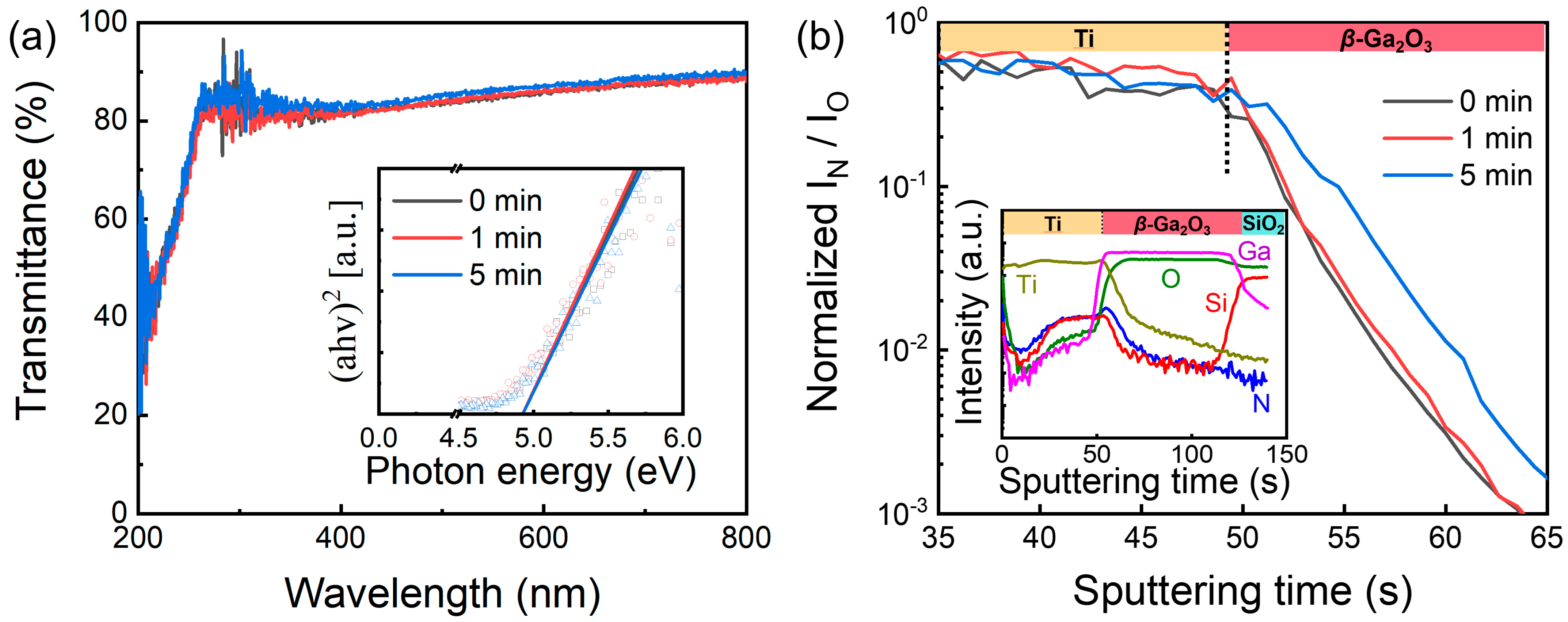
Figure 1a shows the optical transmittance and Tauc plots of the β-Ga2O3 thin film at different PN times. The optical bandgap of each sample was extracted from the linear extrapolation of the inset graph, as shown in Figure 1a. The optical bandgap of the intrinsic β-Ga2O3 thin film was ~4.9 eV, and its value remained almost constant even after PN treatment. This indicated that the PN treatment did not noticeably alter the energy band structure of the β-Ga2O3 semiconductor. The inset of Figure 1b presents a depth profile of the TiN (100 nm)/Ti (5 nm)/intrinsic β-Ga2O3 (100 nm)/SiO2 (300 nm)/Si substrate stack showing a uniform Ga and O atomic concentration in the β-Ga2O3 thin film layer. The SIMS depth profiles of Ga, Ti, N, O and Si remained almost constant regardless of PN treatment time. However, the ratio of N/O concentration at different PN times showed that more N was introduced in the polycrystalline β-Ga2O3 thin films at higher PN times. In detail, the ratio of N/O at 1 min PN treatment was indistinguishable from that of the intrinsic β-Ga2O3. However, the ratio of N/O at 5 min PN treatment was much higher compared to that of the intrinsic β-Ga2O3 and β-Ga2O3 at 1 min PN treatment. This indicated that N was noticeably introduced into the β-Ga2O3 in a logical scale after 5 min PN treatment.
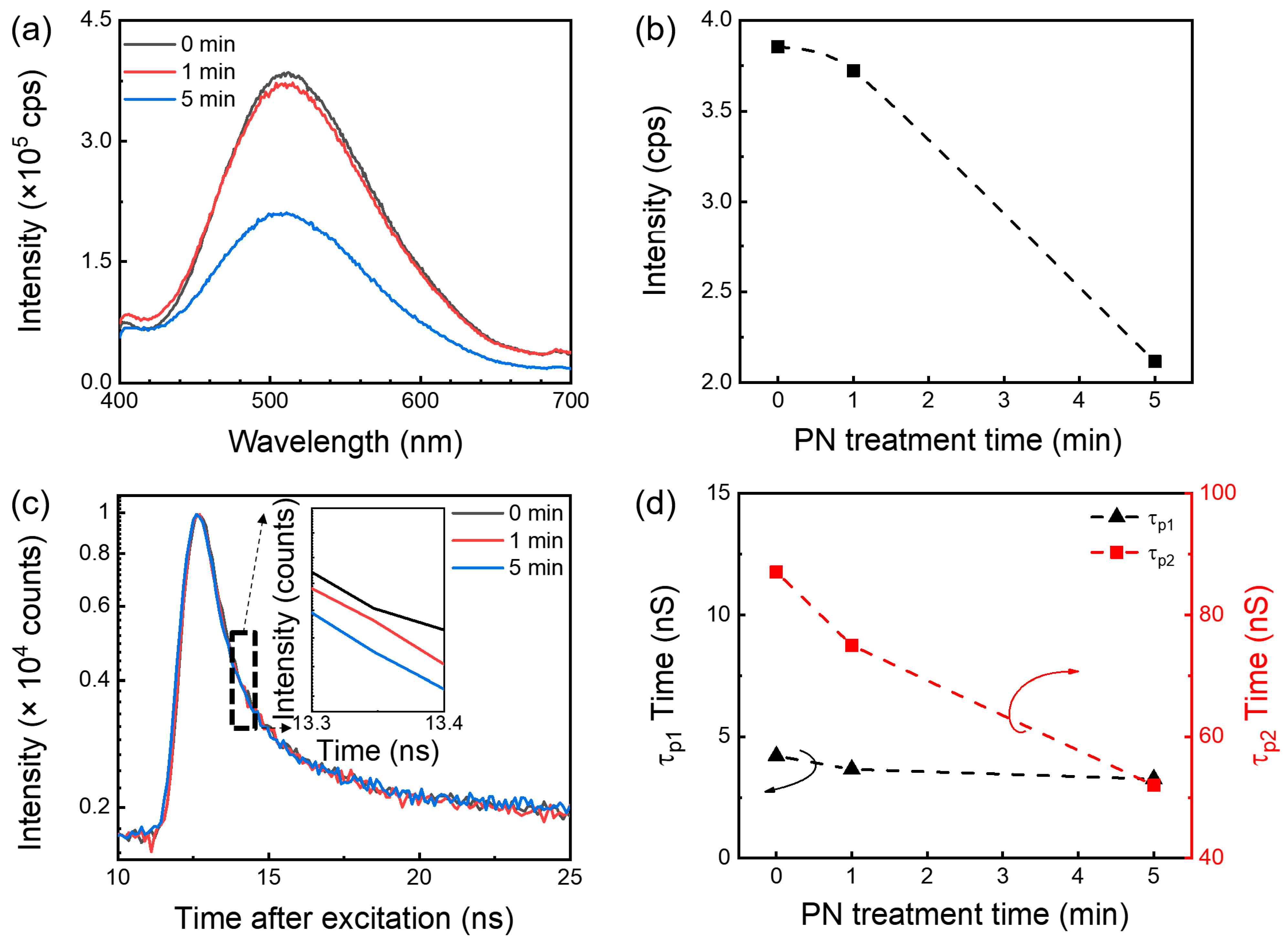
Figure 2a shows the room temperature PL spectrum of the β-Ga2O3 at different PN treatment times. Regardless of the PN treatment, the sputtered β-Ga2O3 thin film exhibited a broad emission band centered around 510 nm. The emission peak in this region presumably originated from the recombination of electrons on donor sites and holes on acceptor sites where the electrons and holes presumably originated from the oxygen vacancy (VO) and gallium vacancy (VGa), respectively [19,20,21]. The peak intensities of 510 nm at different PN times are compared in Figure 2b. The results showed that the PL intensity of the β-Ga2O3 with 5 min PN treatment significantly decreased compared to that of the intrinsic β-Ga2O3 and the β-Ga2O3 with 1 min PN treatment. It was assumed that the N effect on the β-Ga2O3 was negligible for the 1 min PN treatment. However, after 5 min PN treatment, a noticeable amount of N atoms was introduced to the β-Ga2O3, as shown in Figure 1b. The introduced N was presumed to effectively suppress the VO-related electron trap sites, which resulted in the reduction in PL intensity, as shown in Figure 2a,b.
Furthermore, the PL decay profiles at 510 nm are presented at different PN treatment times and the results are compared in Figure 2c. All of the decay curves were approximated by a sum of two exponential functions (τp1 and τp2). τp1 is an instantaneous response to light and represents a fast response component, while τp2 corresponds to the β-Ga2O3 defect and represents a slow response component. Figure 2d exhibits a comparison of τp1 and τp2 at different PN treatment times. This comparison showed that τp1 remained unchanged while τp2 continued to decrease with PN treatment time. The reduced τp2 with PN treatment was attributed to the suppression of the oxygen vacancies via N doping. It was presumed that the N atoms effectively passivated or neutralized the trapping sites.
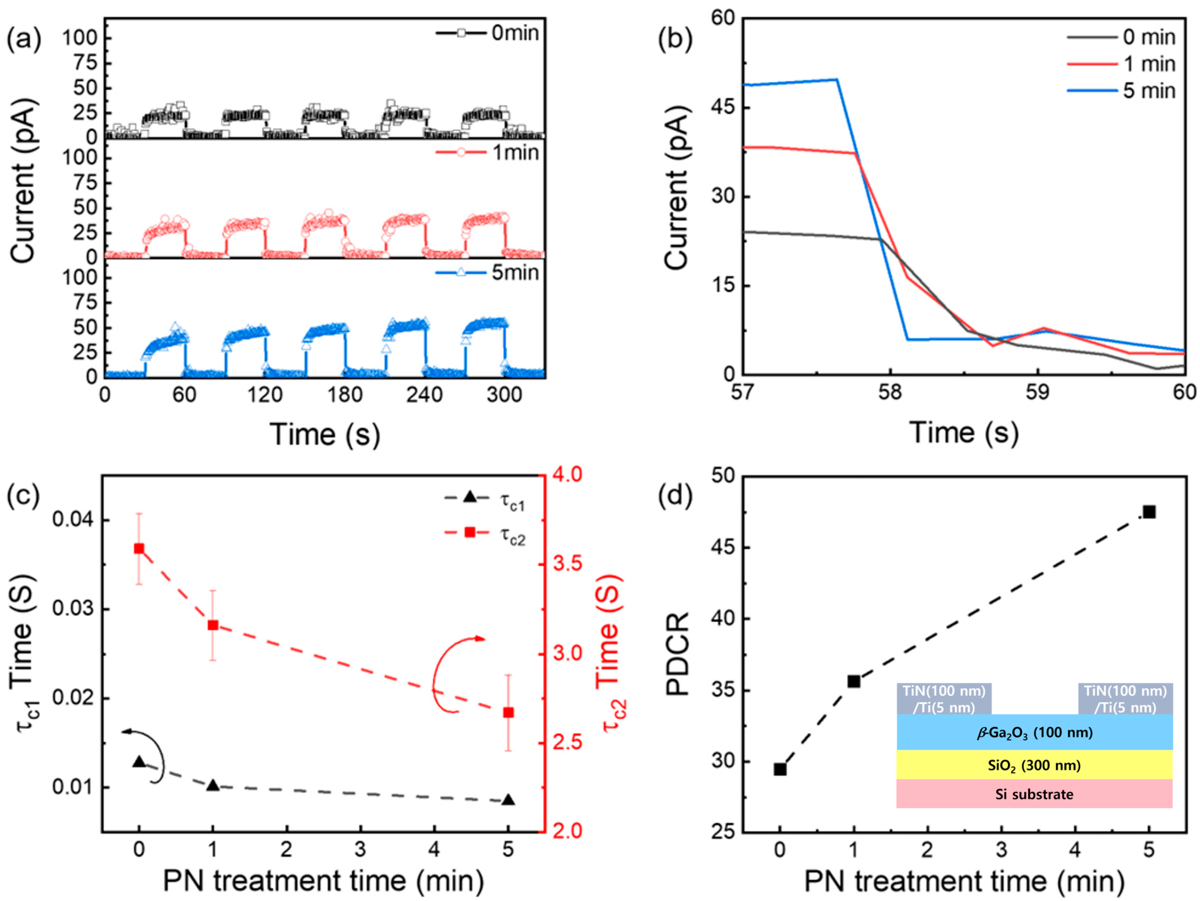
Figure 3a exhibits the transient photo-response of β-Ga2O3 MSM PDs under 254 nm illumination at different PN treatment times. Regardless of the PN treatment, the β-Ga2O3 MSM PDs exhibited a stable repeatability and dark current value as low as 3 pA. A typical photocurrent and its decay time of β-Ga2O3 MSM PDs at different PN treatment times were compared in Figure 3b. The results showed that the photocurrent increased with PN treatment time. The improved photocurrent was attributed to the reduction in the trap density and/or enhancement of carrier mobility via the suppression of trapping sites due to the PN treatment. For a quantitative analysis of the photocurrent decay, the transient curves were fitted using two exponential functions (τc1 and τc2), as shown in Equation (1).
where is the dark current, A and B are constants, and t is the transient time. τc1 and τc2 are the relaxation lifetime decay rate of photo-generated electrons with a fast component (τc1) and a slow component (τc2). The fast component corresponds to the band-to-band transition, while the slow component is attributed to the trapping and de-trapping of photogenerated electrons via defect states. τc1 and τc2 are compared at different PN treatment times in Figure 3c. The results showed that τc1 was less affected by the PN treatment. This was because the band-to-band transition and optical bandgap remained unchanged after PN treatment in these conditions. However, the τc2 values continued to decrease with PN treatment time, indicating that the PN treatment effectively suppressed the trapping and de-trapping processes of the photogenerated electrons via passivating or neutralizing the trapping sites. This is consistent with the results in Figure 2. Finally, photo-to-dark-current (PDCR) of the MSM PD was compared at different PN treatment times, as shown in Figure 3d. The PDCR was defined using Equation (2).
where Ip and Id are the photocurrent and dark current of the PD, respectively. The results showed that the PDCR values continued to enhance with PN treatment time. It was noted that the Id remained unchanged with PN treatment, while the Ip continued to increase due to the reduction in oxygen vacancies or/and enhancement of carrier mobilities.
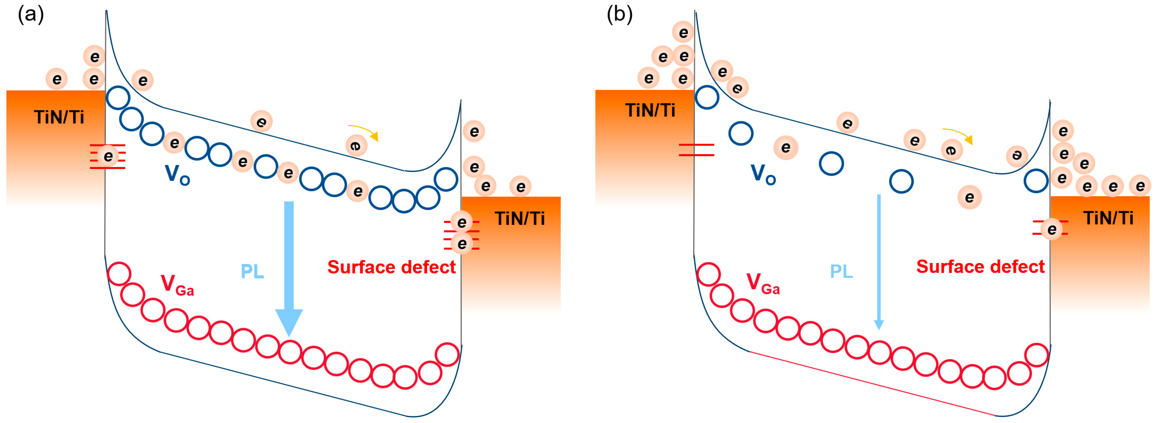
Figure 4 shows a schematic drawing of the trap site distribution with donor and acceptor levels before and after PN treatment. The donor and acceptor bands corresponded to the oxygen vacancies and gallium vacancies, respectively. The schematic image demonstrates that the introduced N atoms were able to passivate or neutralize the trap site below the CB and eventually reduce the electron trapping sites. It is believed that the reduced electron trapping sites resulted in a lower PL intensity, fast decay time, and higher PDCR for the β-Ga2O3 MSM PD with a PN treatment of 5 min.
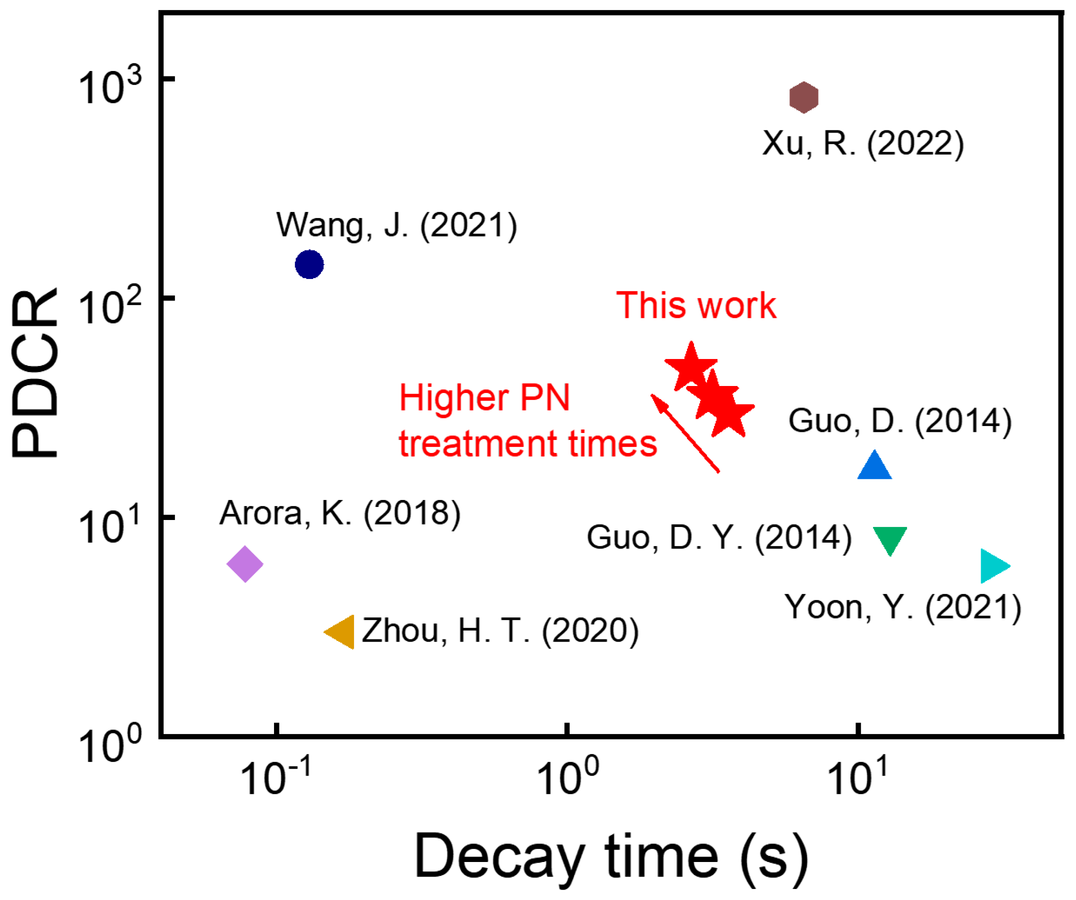
The PDCR and decay time in this work were compared with those of reported β-Ga2O3 based MSM PDs in Figure 5. The results showed that after PN treatment on the polycrystalline β-Ga2O3 thin films, the PDCR value increased but the decay time decreased. It indicated that the device performance of the PDs was enhanced due to the reduction in electron trap sites after PN treatment. This approach could improve the device performance of both electronics and optoelectronics.
4. Conclusions
The effects of plasma nitridation (PN) on polycrystalline β-Ga2O3 thin films were investigated. N atoms were introduced in the polycrystalline β-Ga2O3 thin films via NH3 plasma. The results showed that the PL intensity of the β-Ga2O3 with 5 min PN treatment significantly decreased compared to that of the intrinsic β-Ga2O3 and the β-Ga2O3 with 1 min PN treatment. In addition, the decay time of both the PL and photocurrent decreased after PN treatment for 5 min, which could be explained by the suppression of the trapping and de-trapping processes of the photogenerated electrons via passivating or neutralizing the trapping sites. It was assumed that the introduced N effectively suppressed the VO-related electron trap sites, which resulted in the reduction in the PL intensity, PL decay time, PDCR, and photocurrent decay time. The above results showed that PN treatment on polycrystalline β-Ga2O3 thin films effectively diminished the electron trap sites. This PN treatment technology could improve the device performance of both electronics and optoelectronics.
Author Contributions
Methodology & investigation, S.K. & M.K.; writing—original draft preparation, S.K.; writing—review and editing, J.K. & W.S.H.; supervision, W.S.H. All authors have read and agreed to the published version of the manuscript.
Funding
This work was supported by the Korea Research Institute for defense Technology planning and advancement (KRIT)-Grant funded by the Defense Acquisition Program Administration (DAPA) (KRIT-CT-22-046) & also supported by the K-Sensor Development Program (No. RS-2022-00154729) funded by the Ministry of Trade, Industry and Energy (MOTIE, Republic of Korea).
Institutional Review Board Statement
Not applicable.
Informed Consent Statement
Not applicable.
Data Availability Statement
The data presented in this study are available on request from the corresponding author.
Conflicts of Interest
The authors declare that they have no known competing financial interests or personal relationships that could have influenced the work reported in this paper.
References
- Pearton, S.J.; Yang, J.; Cary, P.H., IV; Ren, F.; Kim, J.; Tadjer, M.J.; Mastro, M.A. A review of Ga2O3 materials, processing, and devices. Appl. Phys. Rev. 2018, 5, 011301. [Google Scholar] [CrossRef] [Green Version]
- Guo, D.; Guo, Q.; Chen, Z.; Wu, Z.; Li, P.; Tang, W. Review of Ga2O3-based optoelectronic devices. Mater. Today Phys. 2019, 11, 100157. [Google Scholar] [CrossRef]
- Chen, X.; Ren, F.; Gu, S.; Ye, J. Review of gallium-oxide-based solar-blind ultraviolet photodetectors. Photonics Res. 2019, 7, 381–415. [Google Scholar] [CrossRef]
- Yoon, Y.; Kim, S.; Lee, I.G.; Cho, B.J.; Hwang, W.S. Electrical and photocurrent properties of a polycrystalline Sn-doped β-Ga2O3 thin film. Mater. Sci. Semicond. Process 2021, 121, 105430. [Google Scholar] [CrossRef]
- Wang, J.; Xiong, Y.; Ye, L.; Li, W.; Qin, G.; Ruan, H. Balanced performance for β-Ga2O3 solar blind photodetectors: The role of oxygen vacancies. Opt. Mater. 2021, 112, 110808. [Google Scholar] [CrossRef]
- Guo, D.; Wu, Z.; Li, P.; An, Y.; Liu, H.; Guo, X. Fabrication of β-Ga2O3 thin films and solar-blind photodetectors by laser MBE technology. Opt. Mater. 2014, 4, 1067–1076. [Google Scholar] [CrossRef]
- Guo, D.Y.; Wu, Z.P.; An, Y.H.; Guo, X.C.; Chu, X.L.; Sun, C.L. Oxygen vacancy tuned Ohmic-Schottky conversion for enhanced performance in β-Ga2O3 solar-blind ultraviolet photodetectors. Appl. Phys. Lett. 2014, 105, 023507. [Google Scholar] [CrossRef]
- Arora, K.; Goel, N.; Kumar, M.; Kumar, M. Ultrahigh performance of self-powered β-Ga2O3 thin film solar-blind photodetector grown on cost-effective Si substrate using high-temperature seed layer. Acs Photonics 2018, 5, 2391–2401. [Google Scholar] [CrossRef]
- Zhou, H.T.; Cong, L.J.; Ma, J.G.; Chen, M.Z.; Song, D.Y.; Wang, H.B. Recent progress of graphene-based photoelectrode materials for dye-sensitized solar cells. J. Alloys Compd. 2020, 847, 156536. [Google Scholar] [CrossRef]
- Xu, R.; Ma, X.; Chen, Y.; Mei, Y.; Ying, L.; Zhang, B.; Long, H. Effect of oxygen vacancies in heteroepitaxial β-Ga2O3 thin film solar blind photodetectors. Mater. Sci. Semin. Proc. 2022, 144, 106621. [Google Scholar] [CrossRef]
- Stepanov, S.I.; Nikolaev, V.I.; Bougrov, V.E.; Romanov, A.E. Epitaxial growth of (2 01) β-Ga2O3 on (0001) sapphire substrates by halide vapour phase epitaxy. Adv. Mater. Sci. 2016, 44, 63–68. [Google Scholar]
- Jankovic, N. Numerical simulations of N-type CdSe poly-TFT electrical characteristics with trap density models of Atlas/Silvaco. Microelectron. Reliab. 2012, 52, 2537–2541. [Google Scholar] [CrossRef]
- Misra, D. Charge-trapping properties of gate oxide grown on nitrogen-implanted silicon substrate. Appl. Phys. Letts. 1999, 75, 2283. [Google Scholar] [CrossRef]
- Dai, M.; Wang, Y.; Shepard, J. Effect of plasma N2 and thermal NH3 nitridation in HfO2 for ultrathin equivalent oxide thickness. J. Appl. Phys. 2013, 113, 044103. [Google Scholar] [CrossRef]
- Park, K.S.; Baek, K.H.; Kim, D.P.; Woo, J.C.; Do, L.M.; No, K.S. Effects of N2 and NH3 remote plasma nitridation on the structural and electrical characteristics of the HfO2 gate dielectrics. Appl. Surf. Sci. 2010, 257, 1347–1350. [Google Scholar] [CrossRef]
- Park, H.B.; Cho, M.J.; Park, J.H. Effects of plasma nitridation of Al2O3 interlayer on thermal stability, fixed charge density, and interfacial trap states of HfO2 gate dielectric films grown by atomic layer deposition. J. Appl. Phys. 2003, 94, 1898. [Google Scholar] [CrossRef]
- Wang, L.; Xu, J.; Liu, L.; Lu, H.; Lai, P. Design of GeSn-based heterojunction-enhanced N-channel tunneling FET with improved subthreshold swing and ON-state current. IEEE Trans. Electron Device 2015, 62, 1235–1240. [Google Scholar]
- Makuła, P.; Pacia, M.; Macyk, W. How to correctly determine the band gap energy of modified semiconductor photocatalysts based on UV–Vis spectra. J. Phys. Chem. Lett. 2018, 9, 6814–6817. [Google Scholar] [CrossRef] [Green Version]
- Chang, K.-W.; Wu, J.-J. Low-Temperature Growth of Well-Aligned β-Ga2O3 Nanowires from a Single-Source Organometallic Precursor. Adv. Mater. 2004, 16, 545–549. [Google Scholar] [CrossRef]
- Tien, L.-C.; Chen, W.-T.; Ho, C.-H. Enhanced photocatalytic activity in β-Ga2O3 nanobelts. J. Am. Ceram. Soc. 2011, 94, 3117–3122. [Google Scholar] [CrossRef]
- Wei, J.; Shi, F. Synthesis and characterization of Sn-doped β-Ga2O3 nano-and micrometer particles by chemical vapor deposition. J. Mater. Sci. Mater. Electron. 2016, 27, 942–946. [Google Scholar] [CrossRef]
Figure 1.
(a) Optical transmittance spectra and Tauc−plot and (b) normalized ratio of N over O from the SIMS depth profile of the β-Ga2O3 thin film at different PN times. In the inset, SIMS depth profile of intrinsic β-Ga2O3 thin film, which was indistinguishable from the depth profile of Ga, O, and N after 1 and 5 min PN treatment time.

Figure 2.
Room temperature PL (a) spectra and (b) peak intensity as a function of PN time. PL decay (c) profile (at 501 nm) and (d) time constant of β-Ga2O3 at different PN treatment times. The arrows indicate each axis.
Figure 2.
Room temperature PL (a) spectra and (b) peak intensity as a function of PN time. PL decay (c) profile (at 501 nm) and (d) time constant of β-Ga2O3 at different PN treatment times. The arrows indicate each axis.

Figure 3.
(a) Transient photo-response, (b) typical photocurrent decay curves, (c) two photocurrent decay time constants (τc1 and τc2), and (d) PDCR of β-Ga2O3 MSM PDs at different PN treatment times. In the inset, schematic cross-sectional image of the MSM PD. The arrows indicate each axis.
Figure 3.
(a) Transient photo-response, (b) typical photocurrent decay curves, (c) two photocurrent decay time constants (τc1 and τc2), and (d) PDCR of β-Ga2O3 MSM PDs at different PN treatment times. In the inset, schematic cross-sectional image of the MSM PD. The arrows indicate each axis.

Figure 4.
Schematic energy band structure of β-Ga2O3 MSM PD with donor and acceptor levels (a) before and (b) after PN treatment. Electron trap sties in blue while hole trap sites in red.
Figure 4.
Schematic energy band structure of β-Ga2O3 MSM PD with donor and acceptor levels (a) before and (b) after PN treatment. Electron trap sties in blue while hole trap sites in red.


Disclaimer/Publisher’s Note: The statements, opinions and data contained in all publications are solely those of the individual author(s) and contributor(s) and not of MDPI and/or the editor(s). MDPI and/or the editor(s) disclaim responsibility for any injury to people or property resulting from any ideas, methods, instructions or products referred to in the content. |
© 2023 by the authors. Licensee MDPI, Basel, Switzerland. This article is an open access article distributed under the terms and conditions of the Creative Commons Attribution (CC BY) license (https://creativecommons.org/licenses/by/4.0/).
Share and Cite
MDPI and ACS Style
Kim, S.; Kim, M.; Kim, J.; Hwang, W.S. Plasma Nitridation Effect on β-Ga2O3 Semiconductors. Nanomaterials 2023, 13, 1199. https://doi.org/10.3390/nano13071199
AMA Style
Kim S, Kim M, Kim J, Hwang WS. Plasma Nitridation Effect on β-Ga2O3 Semiconductors. Nanomaterials. 2023; 13(7):1199. https://doi.org/10.3390/nano13071199
Chicago/Turabian StyleKim, Sunjae, Minje Kim, Jihyun Kim, and Wan Sik Hwang. 2023. "Plasma Nitridation Effect on β-Ga2O3 Semiconductors" Nanomaterials 13, no. 7: 1199. https://doi.org/10.3390/nano13071199
Note that from the first issue of 2016, this journal uses article numbers instead of page numbers. See further details here.