
Enhanced Electroluminescence from a Silicon Nanocrystal/Silicon Carbide Multilayer Light-Emitting Diode
 and
and 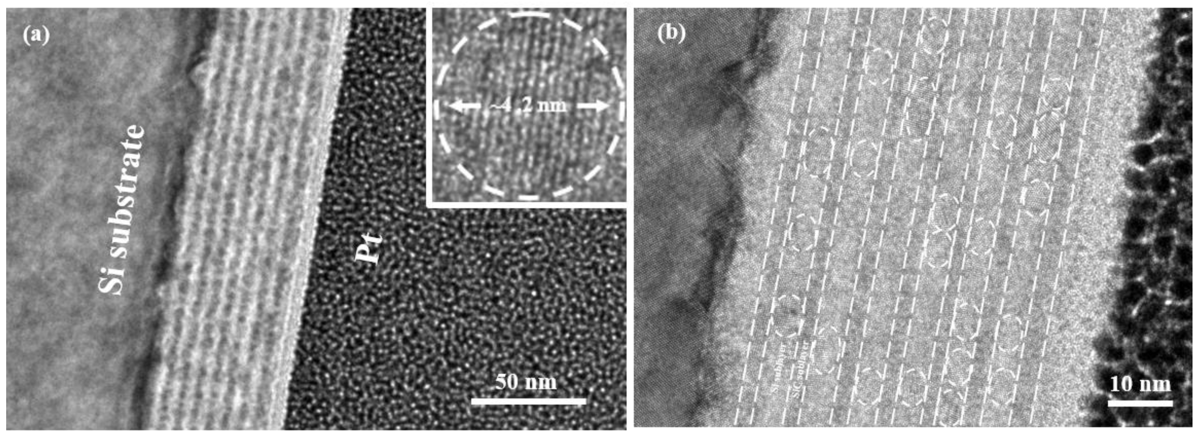
Abstract
:1. Introduction
2. Experiment
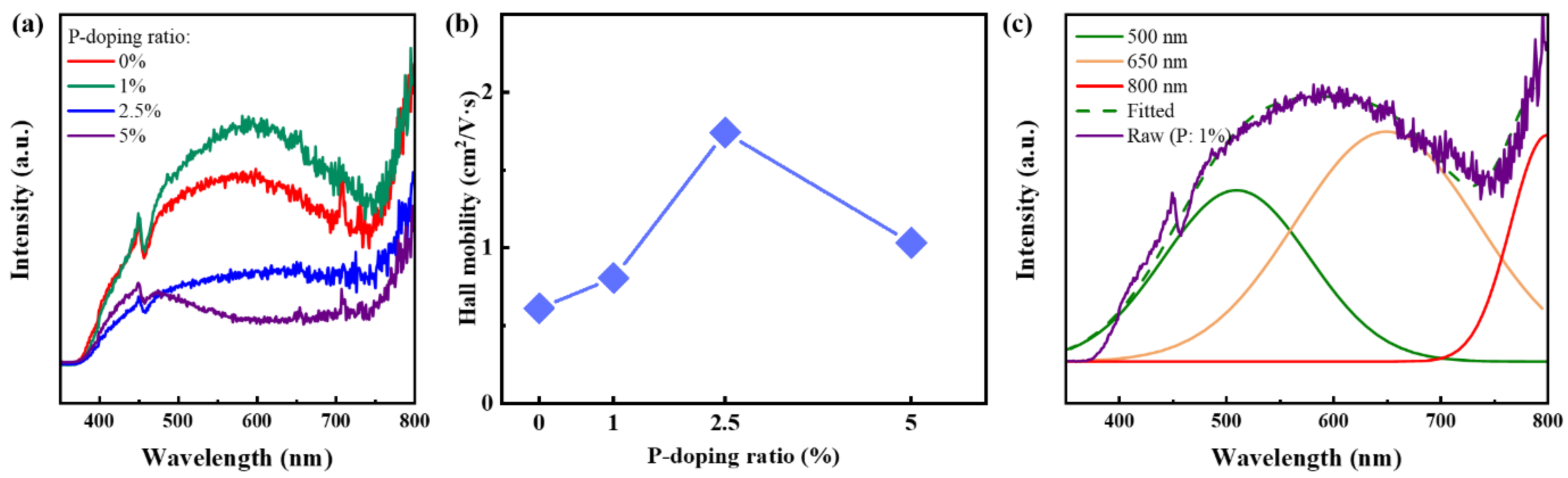
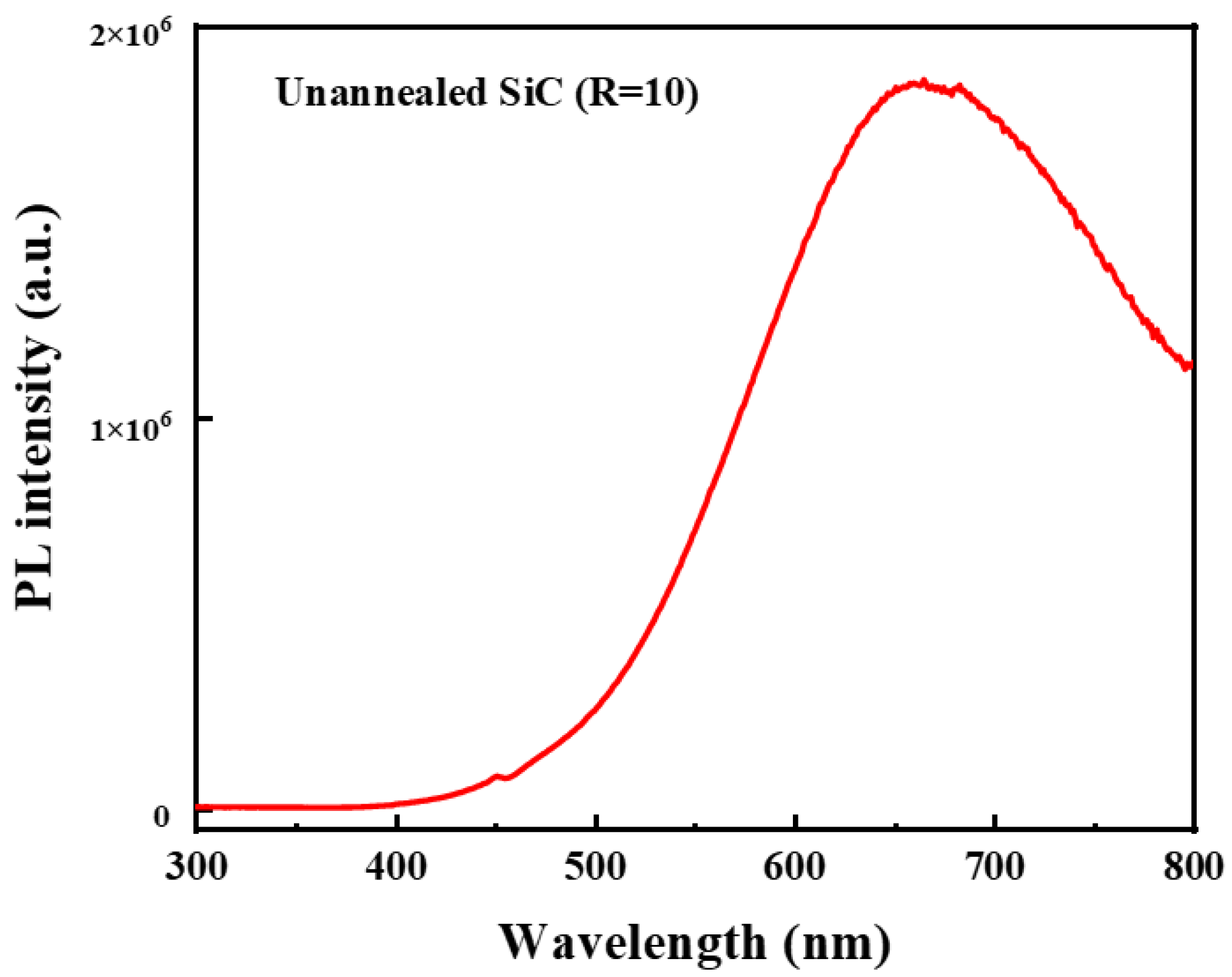
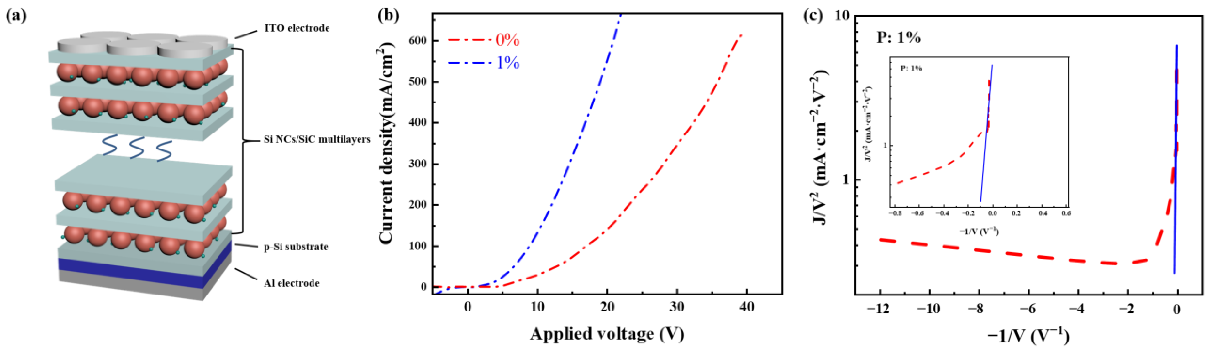
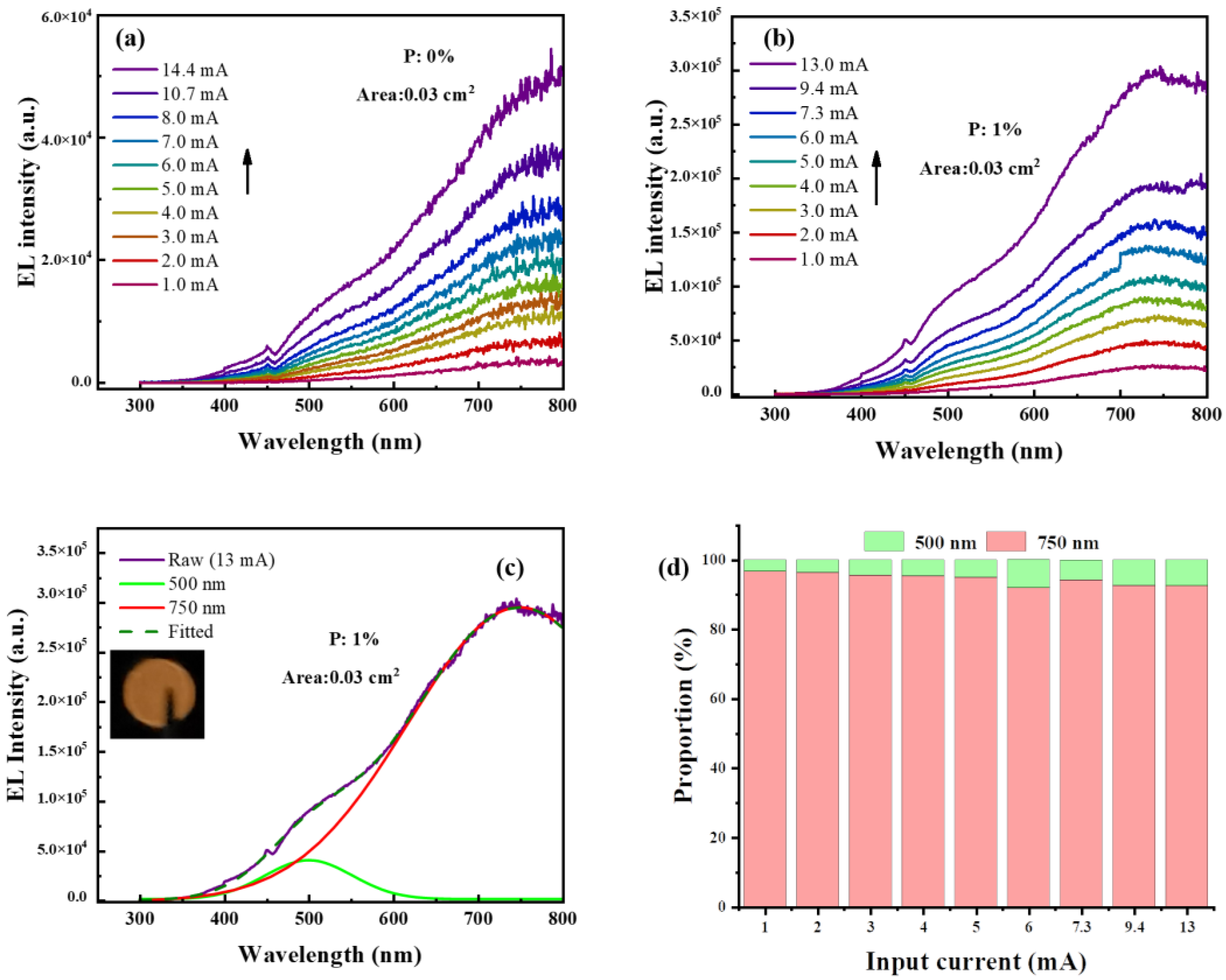
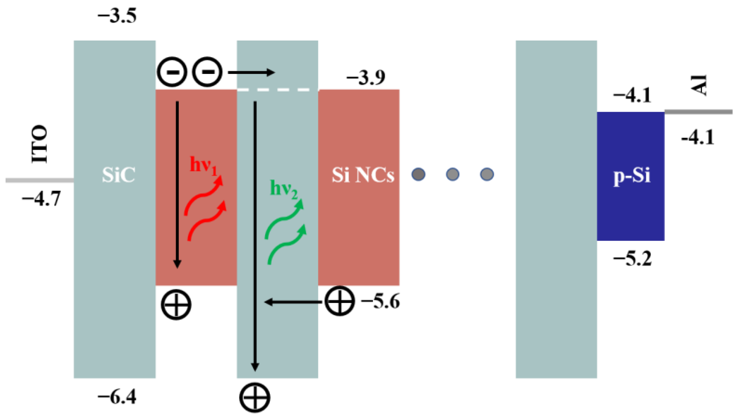
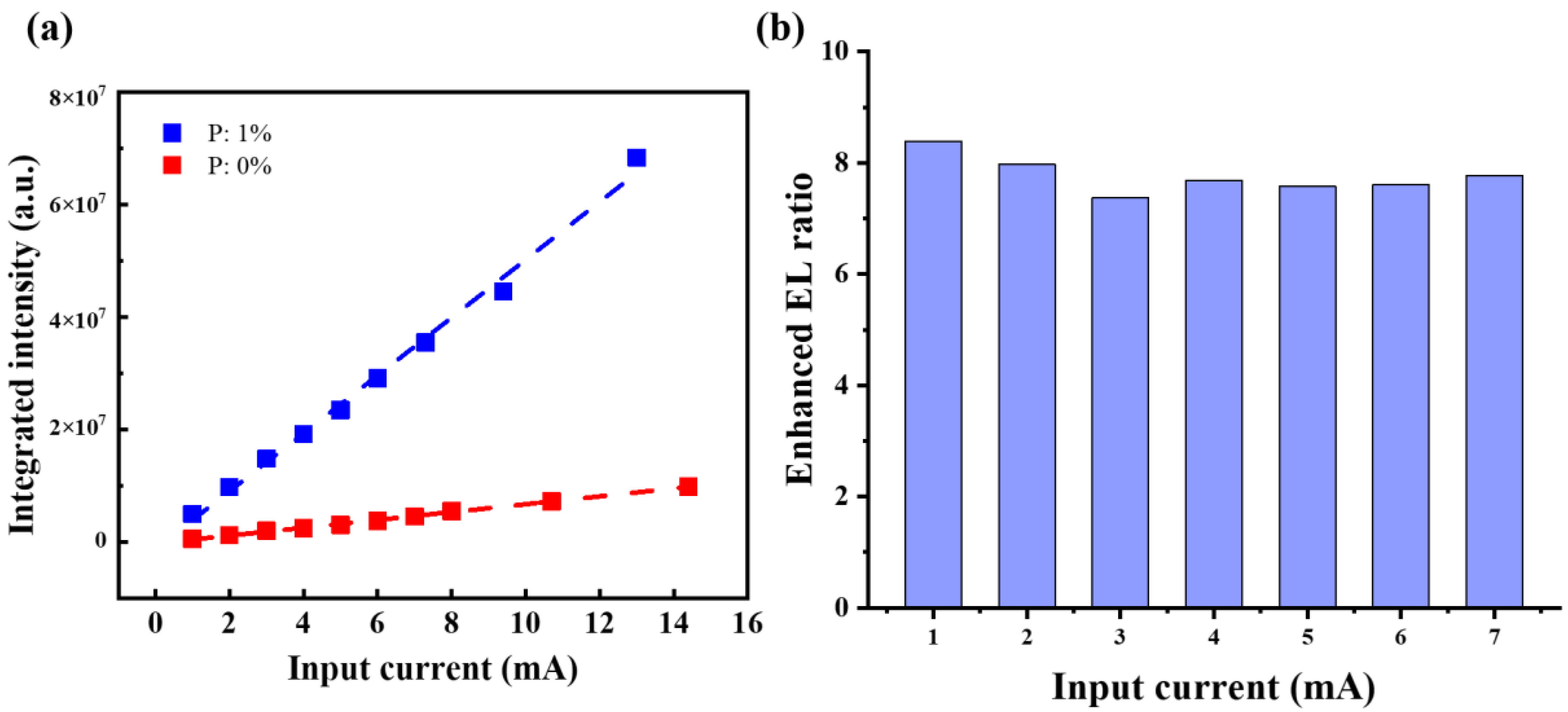
3. Results and Discussion
4. Conclusions
Supplementary Materials
Author Contributions
Funding
Data Availability Statement
Conflicts of Interest
References
- Whitworth, G.L.; Dalmases, M.; Taghipour, N.; Konstantatos, G. Solution-Processed PbS Quantum Dot Infrared Laser with Room-Temperature Tunable Emission in the Optical Telecommunications Window. Nat. Photonics 2021, 15, 738–742. [Google Scholar] [CrossRef]
- Tatsuura, S.; Furuki, M.; Sato, Y.; Iwasa, I.; Tian, M.; Mitsu, H. Semiconductor Carbon Nanotubes as Ultrafast Switching Materials for Optical Telecommunications. Adv. Mater. 2003, 15, 534–537. [Google Scholar] [CrossRef]
- Fernandez-Gonzalvo, X.; Chen, Y.-H.; Yin, C.; Rogge, S.; Longdell, J.J. Coherent Frequency Up-Conversion of Microwaves to the Optical Telecommunications Band in an Er:YSO Crystal. Phys. Rev. A 2015, 92, 062313. [Google Scholar] [CrossRef] [Green Version]
- Leonardi, A.A.; Lo Faro, M.J.; Irrera, A. Biosensing Platforms Based on Silicon Nanostructures: A Critical Review. Anal. Chim. Acta 2021, 1160, 338393. [Google Scholar] [CrossRef]
- Dohnalová, K.; Poddubny, A.N.; Prokofiev, A.A.; de Boer, W.D.; Umesh, C.P.; Paulusse, J.M.; Zuilhof, H.; Gregorkiewicz, T. Surface Brightens up Si Quantum Dots: Direct Bandgap-like Size-Tunable Emission. Light Sci. Appl. 2013, 2, e47. [Google Scholar] [CrossRef] [Green Version]
- Marinins, A.; Zandi Shafagh, R.; van der Wijngaart, W.; Haraldsson, T.; Linnros, J.; Veinot, J.G.C.; Popov, S.; Sychugov, I. Light-Converting Polymer/Si Nanocrystal Composites with Stable 60–70% Quantum Efficiency and Their Glass Laminates. ACS Appl. Mater. Interfaces 2017, 9, 30267–30272. [Google Scholar] [CrossRef]
- de Boer, W.D.A.M.; Timmerman, D.; Dohnalová, K.; Yassievich, I.N.; Zhang, H.; Buma, W.J.; Gregorkiewicz, T. Red Spectral Shift and Enhanced Quantum Efficiency in Phonon-Free Photoluminescence from Silicon Nanocrystals. Nat. Nanotechnol. 2010, 5, 878–884. [Google Scholar] [CrossRef]
- Sugimoto, H.; Zhou, H.; Takada, M.; Fushimi, J.; Fujii, M. Visible-Light Driven Photocatalytic Hydrogen Generation by Water-Soluble All-Inorganic Core–Shell Silicon Quantum Dots. J. Mater. Chem. A 2020, 8, 15789–15794. [Google Scholar] [CrossRef]
- Ono, T.; Xu, Y.; Sakata, T.; Saitow, K. Designing Efficient Si Quantum Dots and LEDs by Quantifying Ligand Effects. ACS Appl. Mater. Interfaces 2022, 14, 1373–1388. [Google Scholar] [CrossRef] [PubMed]
- Xin, Y.; Nishio, K.; Saitow, K. White-Blue Electroluminescence from a Si Quantum Dot Hybrid Light-Emitting Diode. Appl. Phys. Lett. 2015, 106, 201102. [Google Scholar] [CrossRef]
- Maier-Flaig, F.; Rinck, J.; Stephan, M.; Bocksrocker, T.; Bruns, M.; Kübel, C.; Powell, A.K.; Ozin, G.A.; Lemmer, U. Multicolor Silicon Light-Emitting Diodes (SiLEDs). Nano Lett. 2013, 13, 475–480. [Google Scholar] [CrossRef]
- Sarkar, A.; Bar, R.; Singh, S.; Chowdhury, R.K.; Bhattacharya, S.; Das, A.K.; Ray, S.K. Size-Tunable Electroluminescence Characteristics of Quantum Confined Si Nanocrystals Embedded in Si-Rich Oxide Matrix. Appl. Phys. Lett. 2020, 116, 231105. [Google Scholar] [CrossRef]
- Hao, X.J.; Cho, E.-C.; Scardera, G.; Shen, Y.S.; Bellet-Amalric, E.; Bellet, D.; Conibeer, G.; Green, M.A. Phosphorus-Doped Silicon Quantum Dots for All-Silicon Quantum Dot Tandem Solar Cells. Sol. Energy Mater. Sol. Cells 2009, 93, 1524–1530. [Google Scholar] [CrossRef]
- Hao, X.J.; Cho, E.-C.; Flynn, C.; Shen, Y.S.; Park, S.C.; Conibeer, G.; Green, M.A. Synthesis and Characterization of Boron-Doped Si Quantum Dots for All-Si Quantum Dot Tandem Solar Cells. Sol. Energy Mater. Sol. Cells 2009, 93, 273–279. [Google Scholar] [CrossRef]
- Fujii, M.; Mimura, A.; Hayashi, S.; Yamamoto, Y.; Murakami, K. Hyperfine Structure of the Electron Spin Resonance of Phosphorus-Doped Si Nanocrystals. Phys. Rev. Lett. 2002, 89, 206805. [Google Scholar] [CrossRef] [PubMed] [Green Version]
- Sun, T.; Li, D.; Chen, J.; Han, J.; Zhu, T.; Li, W.; Xu, J.; Chen, K. Electron Spin Resonance in P-Doped Si Nanocrystals/SiC Stacked Structures with Various Dot Sizes. Appl. Surf. Sci. 2023, 613, 155983. [Google Scholar] [CrossRef]
- Oliva-Chatelain, L.; Ticich, M.; Barron, R. Doping Silicon Nanocrystals and Quantum Dots. Nanoscale 2016, 8, 1733–1745. [Google Scholar] [CrossRef] [PubMed]
- Lu, P.; Mu, W.; Xu, J.; Zhang, X.; Zhang, W.; Li, W.; Xu, L.; Chen, K. Phosphorus Doping in Si Nanocrystals/SiO2 Multilayers and Light Emission with Wavelength Compatible for Optical Telecommunication. Sci. Rep. 2016, 6, 22888. [Google Scholar] [CrossRef] [Green Version]
- Li, D.; Chen, J.; Sun, T.; Zhang, Y.; Xu, J.; Li, W.; Chen, K. Enhanced Subband Light Emission from Si Quantum Dots/SiO2 Multilayers via Phosphorus and Boron Co-Doping. Opt. Express 2022, 30, 12308. [Google Scholar] [CrossRef]
- Jiang, Y.; Li, D.; Xu, J.; Li, W.; Chen, K. Size-Dependent Phosphorus Doping Effect in Nanocrystalline-Si-Based Multilayers. Appl. Surf. Sci. 2018, 461, 66–71. [Google Scholar] [CrossRef]
- Kocevski, V.; Eriksson, O.; Rusz, J. Band Alignment Switching and the Interaction between Neighboring Silicon Nanocrystals Embedded in a SiC Matrix. Phys. Rev. B 2015, 91, 165429. [Google Scholar] [CrossRef]
- Molla, M.Z.; Zhigunov, D.; Noda, S.; Samukawa, S. Structural Optimization and Quantum Size Effect of Si-Nanocrystals in SiC Interlayer Fabricated with Bio-Template. Mater. Res. Express 2019, 6, 065059. [Google Scholar] [CrossRef]
- Das, D.; Sain, B. Electrical Transport Phenomena Prevailing in Undoped Nc-Si/a-SiNx:H Thin Films Prepared by Inductively Coupled Plasma Chemical Vapor Deposition. J. Appl. Phys. 2013, 114, 073708. [Google Scholar] [CrossRef]
- Sun, T.; Li, D.; Chen, J.; Han, J.; Li, W.; Xu, J.; Chen, K. Temperature-Dependent Carrier Transport Behaviors in Phosphorus-Doped Silicon Nanocrystals/Silicon Carbide Multilayers. Vacuum 2023, 207, 111657. [Google Scholar] [CrossRef]
- Rui, Y.; Li, S.; Xu, J.; Cao, Y.; Li, W.; Chen, K. Comparative Study of Electroluminescence from Annealed Amorphous SiC Single Layer and Amorphous Si/SiC Multilayers. J. Non-Cryst. Solids 2012, 358, 2114–2117. [Google Scholar] [CrossRef]
- Rui, Y.; Li, S.; Cao, Y.; Xu, J.; Li, W.; Chen, K. Structural and Electroluminescent Properties of Si Quantum Dots/SiC Multilayers. Appl. Surf. Sci. 2013, 269, 37–40. [Google Scholar] [CrossRef]
- Rui, Y.; Li, S.; Xu, J.; Song, C.; Jiang, X.; Li, W.; Chen, K.; Wang, Q.; Zuo, Y. Size-Dependent Electroluminescence from Si Quantum Dots Embedded in Amorphous SiC Matrix. J. Appl. Phys. 2011, 110, 064322. [Google Scholar] [CrossRef]
- Fujii, M.; Mimura, A.; Hayashi, S.; Yamamoto, K.; Urakawa, C.; Ohta, H. Improvement in Photoluminescence Efficiency of SiO2 Films Containing Si Nanocrystals by P Doping: An Electron Spin Resonance Study. J. Appl. Phys. 2000, 87, 1855–1857. [Google Scholar] [CrossRef] [Green Version]
- Li, D.; Jiang, Y.; Zhang, P.; Shan, D.; Xu, J.; Li, W.; Chen, K. The Phosphorus and Boron Co-Doping Behaviors at Nanoscale in Si Nanocrystals/SiO2 Multilayers. Appl. Phys. Lett. 2017, 110, 233105. [Google Scholar] [CrossRef]
- Joo, B.S.; Jang, S.; Gu, M.; Jung, N.; Han, M. Effect of Auger Recombination Induced by Donor and Acceptor States on Luminescence Properties of Silicon Quantum Dots/SiO2 Multilayers. J. Alloys Compd. 2019, 801, 568–572. [Google Scholar] [CrossRef]
- Fujii, M.; Hayashi, S.; Yamamoto, K. Photoluminescence from B-Doped Si Nanocrystals. J. Appl. Phys. 1998, 83, 7953–7957. [Google Scholar] [CrossRef] [Green Version]
- Kayanuma, Y. Quantum-Size Effects of Interacting Electrons and Holes in Semiconductor Microcrystals with Spherical Shape. Phys. Rev. B 1988, 38, 9797–9805. [Google Scholar] [CrossRef]
- Brus, L.E. Electron-Electron and Electron-hole Interactions in Small Semiconductor Crystallites: The Size Dependence of the Lowest Excited Electronic State. J. Chem. Phys. 1984, 80, 4403–4409. [Google Scholar] [CrossRef] [Green Version]
- Jiang, C.-W.; Green, M.A. Silicon Quantum Dot Superlattices: Modeling of Energy Bands, Densities of States, and Mobilities for Silicon Tandem Solar Cell Applications. J. Appl. Phys. 2006, 99, 114902. [Google Scholar] [CrossRef]
- Xu, X.; Cao, Y.Q.; Lu, P.; Xu, J.; Li, W.; Chen, K.J. Electroluminescence Devices Based on Si Quantum Dots/SiC Multilayers Embedded in PN Junction. IEEE Photonics J. 2014, 6, 1–7. [Google Scholar] [CrossRef]
- Hay, R.S.; Fair, G.E.; Bouffioux, R.; Urban, E.; Morrow, J.; Hart, A.; Wilson, M. Hi-NicalonTM-S SiC Fiber Oxidation and Scale Crystallization Kinetics. J. Am. Ceram. Soc. 2011, 94, 3983–3991. [Google Scholar] [CrossRef]
- Takeda, M.; Urano, A.; Sakamoto, J.; Imai, Y. Microstructure and Oxidation Behavior of Silicon Carbide Fibers Derived from Polycarbosilane. J. Am. Ceram. Soc. 2004, 83, 1171–1176. [Google Scholar] [CrossRef]
- Chen, G.; Chen, S.; Lin, Z.; Huang, R.; Guo, Y. Enhanced Red Emission from Amorphous Silicon Carbide Films via Nitrogen Doping. Micromachines 2022, 13, 2043. [Google Scholar] [CrossRef]
- Zanatta, A.R. Revisiting the Optical Bandgap of Semiconductors and the Proposal of a Unified Methodology to Its Determination. Sci. Rep. 2019, 9, 11225. [Google Scholar] [CrossRef] [Green Version]
- Ni, Z.; Zhou, S.; Zhao, S.; Peng, W.; Yang, D.; Pi, X. Silicon Nanocrystals: Unfading Silicon Materials for Optoelectronics. Mater. Sci. Eng. R Rep. 2019, 138, 85–117. [Google Scholar] [CrossRef]
- Swain, B.P.; Dusane, R.O. Multiphase Structure of Hydrogen Diluted A-SiC:H Deposited by HWCVD. Mater. Chem. Phys. 2006, 99, 240–246. [Google Scholar] [CrossRef]
- Fuad, A.; Kultsum, U.; Taufiq, A.; Hartatiek. Low-Temperature Synthesis of α-SiC (6H-SiC) Nanoparticles with Magnesium Catalyst. Mater. Today Proc. 2019, 17, 1451–1457. [Google Scholar] [CrossRef]
- Xu, J.; Mei, J.; Rui, Y.; Chen, D.; Cen, Z.; Li, W.; Ma, Z.; Xu, L.; Huang, X.; Chen, K. UV and Blue Light Emission from SiC Nanoclusters in Annealed Amorphous SiC Alloys. J. Non-Cryst. Solids 2006, 352, 1398–1401. [Google Scholar] [CrossRef]
- Kořínek, M.; Schnabel, M.; Canino, M.; Kozák, M.; Trojánek, F.; Salava, J.; Löper, P.; Janz, S.; Summonte, C.; Malý, P. Influence of Boron Doping and Hydrogen Passivation on Recombination of Photoexcited Charge Carriers in Silicon Nanocrystal/SiC Multilayers. J. Appl. Phys. 2013, 114, 073101. [Google Scholar] [CrossRef]
- Gallis, S.; Nikas, V.; Suhag, H.; Huang, M.; Kaloyeros, A.E. White Light Emission from Amorphous Silicon Oxycarbide (a-SiCxOy) Thin Films: Role of Composition and Postdeposition Annealing. Appl. Phys. Lett. 2010, 97, 081905. [Google Scholar] [CrossRef]
- Wang, C.; Zhou, J.; Song, M.; Chen, X.; Zheng, Y.; Xia, W. Modification of Plasma-Generated SiC Nanoparticles by Heat Treatment under Air Atmosphere. J. Alloys Compd. 2022, 900, 163507. [Google Scholar] [CrossRef]
- Lin, G.-R.; Lin, C.-J.; Kuo, H.-C. Improving Carrier Transport and Light Emission in a Silicon-Nanocrystal Based MOS Light-Emitting Diode on Silicon Nanopillar Array. Appl. Phys. Lett. 2007, 91, 093122. [Google Scholar] [CrossRef]
- Takagahara, T.; Takeda, K. Theory of the Quantum Confinement Effect on Excitons in Quantum Dots of Indirect-Gap Materials. Phys. Rev. B 1992, 46, 15578–15581. [Google Scholar] [CrossRef] [PubMed]
- Vinciguerra, V.; Franzò, G.; Priolo, F.; Iacona, F.; Spinella, C. Quantum Confinement and Recombination Dynamics in Silicon Nanocrystals Embedded in Si/SiO2 Superlattices. J. Appl. Phys. 2000, 87, 8165–8173. [Google Scholar] [CrossRef]
- Cao, Y.; Xu, J.; Ge, Z.; Zhai, Y.; Li, W.; Jiang, X.; Chen, K. Enhanced Broadband Spectral Response and Energy Conversion Efficiency for Hetero-Junction Solar Cells with Graded-Sized Si Quantum Dots/SiC Multilayers. J. Mater. Chem. C 2015, 3, 12061–12067. [Google Scholar] [CrossRef]
- Xu, X.; Zhu, T.; Xiao, K.; Zhu, Y.; Chen, J.; Li, D.; Xu, L.; Xu, J.; Chen, K. High-Efficiency Air-Processed Si-Based Perovskite Light-Emitting Devices via PMMA-TBAPF6 Co-Doping. Adv. Opt. Mater. 2022, 10, 2102848. [Google Scholar] [CrossRef]
- Xu, X.; Xiao, K.; Hou, G.; Zhu, Y.; Zhu, T.; Xu, L.; Xu, J.; Chen, K. Air-Processed Stable near-Infrared Si-Based Perovskite Light-Emitting Devices with Efficiency Exceeding 7.5%. J. Mater. Chem. C 2022, 10, 1276–1281. [Google Scholar] [CrossRef]
- van Buuren, T.; Dinh, L.N.; Chase, L.L.; Siekhaus, W.J.; Terminello, L.J. Changes in the Electronic Properties of Si Nanocrystals as a Function of Particle Size. Phys. Rev. Lett. 1998, 80, 3803–3806. [Google Scholar] [CrossRef]
- Warga, J.; Li, R.; Basu, S.N.; Dal Negro, L. Electroluminescence from Silicon-Rich Nitride/Silicon Superlattice Structures. Appl. Phys. Lett. 2008, 93, 151116. [Google Scholar] [CrossRef]


Disclaimer/Publisher’s Note: The statements, opinions and data contained in all publications are solely those of the individual author(s) and contributor(s) and not of MDPI and/or the editor(s). MDPI and/or the editor(s) disclaim responsibility for any injury to people or property resulting from any ideas, methods, instructions or products referred to in the content. |
© 2023 by the authors. Licensee MDPI, Basel, Switzerland. This article is an open access article distributed under the terms and conditions of the Creative Commons Attribution (CC BY) license (https://creativecommons.org/licenses/by/4.0/).
Share and Cite
Sun, T.; Li, D.; Chen, J.; Wang, Y.; Han, J.; Zhu, T.; Li, W.; Xu, J.; Chen, K. Enhanced Electroluminescence from a Silicon Nanocrystal/Silicon Carbide Multilayer Light-Emitting Diode. Nanomaterials 2023, 13, 1109. https://doi.org/10.3390/nano13061109
Sun T, Li D, Chen J, Wang Y, Han J, Zhu T, Li W, Xu J, Chen K. Enhanced Electroluminescence from a Silicon Nanocrystal/Silicon Carbide Multilayer Light-Emitting Diode. Nanomaterials. 2023; 13(6):1109. https://doi.org/10.3390/nano13061109
Chicago/Turabian StyleSun, Teng, Dongke Li, Jiaming Chen, Yuhao Wang, Junnan Han, Ting Zhu, Wei Li, Jun Xu, and Kunji Chen. 2023. "Enhanced Electroluminescence from a Silicon Nanocrystal/Silicon Carbide Multilayer Light-Emitting Diode" Nanomaterials 13, no. 6: 1109. https://doi.org/10.3390/nano13061109