Article

Enhanced Magnetism and Anomalous Hall Transport through Two-Dimensional Tungsten Disulfide Interfaces

1
Department of Physics, University of South Florida, Tampa, FL 33620, USA
2
Department of Physics, The Pennsylvania State University, University Park, PA 16802, USA
*
Authors to whom correspondence should be addressed.
Nanomaterials 2023, 13(4), 771; https://doi.org/10.3390/nano13040771
Submission received: 31 January 2023 / Revised: 14 February 2023 / Accepted: 16 February 2023 / Published: 18 February 2023
(This article belongs to the Special Issue Nano-Structured Thin Films: Growth, Characteristics, and Application)

Abstract

:
The magnetic proximity effect (MPE) has recently been explored to manipulate interfacial properties of two-dimensional (2D) transition metal dichalcogenide (TMD)/ferromagnet heterostructures for use in spintronics and valleytronics. However, a full understanding of the MPE and its temperature and magnetic field evolution in these systems is lacking. In this study, the MPE has been probed in Pt/WS2/BPIO (biphase iron oxide, Fe3O4 and α-Fe2O3) heterostructures through a comprehensive investigation of their magnetic and transport properties using magnetometry, four-probe resistivity, and anomalous Hall effect (AHE) measurements. Density functional theory (DFT) calculations are performed to complement the experimental findings. We found that the presence of monolayer WS2 flakes reduces the magnetization of BPIO and hence the total magnetization of Pt/WS2/BPIO at T > ~120 K—the Verwey transition temperature of Fe3O4 (TV). However, an enhanced magnetization is achieved at T < TV. In the latter case, a comparative analysis of the transport properties of Pt/WS2/BPIO and Pt/BPIO from AHE measurements reveals ferromagnetic coupling at the WS2/BPIO interface. Our study forms the foundation for understanding MPE-mediated interfacial properties and paves a new pathway for designing 2D TMD/magnet heterostructures for applications in spintronics, opto-spincaloritronics, and valleytronics.

1. Introduction

Recently, two-dimensional transition metal dichalcogenides (2D-TMDs) have attracted a great deal of attention due to their extraordinary bandgap tunability, high optical sensitivity, strong spin orbit coupling, and low symmetry structure, making this a fascinating class of materials for spintronics, valleytronics, and spin caloritronics [1,2,3,4]. Spin degeneracy in momentum space at K and K′ valley facilitates controllable spin polarization as detected by the helicity dependence of optical techniques such as magnetic circular dichroism [5] (MCD) and polarization resolved photoluminescence (PL). To enhance valley polarization, various approaches such as defect engineering [6], chemical doping [7], electrical doping [8], and TMD/FM (FM = ferro/ferrimagnet) heterostructures [5,9,10,11,12] have been exploited. Among these, TMD/FM heterostructures based on spin orbit coupling [13], charge transfer [9,14], and magnetic proximity effect [5,10] (MPE) are of topical interest. The MPE, an interfacial magnetic phenomenon due to the exchange coupling based on interfacial orbital hybridization [15]. Antiferromagnetic (AFM) exchange coupling was observed at the MoS2/yttrium iron garnet (YIG) interface by the MCD measurements at room temperature, where MoS2 flakes were transferred onto a YIG film via a wet transfer technique [5]. The ferromagnetic signal was detected in the MoS2 layer, induced by the ferrimagnetic YIG layer via the MPE. Density functional theory (DFT) calculations also reveal the charge transfer from YIG to MoS2 and the formation of n-type MoS2. However, Peng et al. reported the absence of MPE in the MoS2/YIG heterostructure [16]. This discrepancy may arise from the fact that the process of transferring 2D-TMDs to a magnetic substrate (via a wet or dry transfer process) affects the distance between the van der Waals material and the magnetic substrate and hence the strength of the orbital hybridization or the strength of the MPE. MoSe2 transferred onto La0.7Sr0.3MnO3 (LSMO) shows a reduction of the magnetization due to a destabilization of the double exchange coupling of Mn3+-O-Mn4+ at the MoSe2/LSMO interface by charge transfer [9]. On the other hand, Zhang et al. reported that the insertion of h-BN between MoSe2 and LSMO enhanced the valley splitting by the MPE [9]. These studies highlight that both charge transfer and the MPE are crucial for controlling the interfacial magnetic properties. A full understanding of such interfacial properties is the key to unlocking doors to the applications of spin-based nanodevices [17]. Interfacing YIG with graphene (Gr) can induce the MPE in the Gr layer as observed in magnetoresistance (MR) and spin pumping by the inverse Rashba effect [18]. Pulsed laser deposition grown MoS2/CoFe2O4 shows an enhanced MR effect when the number of MoS2 layers is reduced below 10 [19]. Since monolayer MoS2 exhibits relatively large spin orbit coupling and generates spin accumulation and spin injection, it may be responsible for the MR enhancement. The presence of an intermediate WSe2 monolayer (ML) has recently been shown to enhance the spin-charge conversion process, giving rise to the giant spin Seebeck effect in Pt/ML-WSe2/YIG [20]. First-principles calculations indicate the spin-Seebeck coefficient enhancement after the insertion of monolayer WSe2 between Fe and Pt layers in Pt/WSe2/Fe relative to Fe/Pt, due to the increases of the total density of state near the Fermi level and the magnetization [21]. In another study, first-principles calculations show the MPE when monolayer WS2 is placed on top of EuS [22]. Depending on the Eu- or S-surface termination, the interface with WS2 can exhibit ferromagnetic or antiferromagnetic ordering, which is also correlated with the distance between WS2 and EuS termination. Overall, previous works on different TMD/FM heterostructures mostly focused on magnetic insulators (e.g., YIG and EuS) that possess magnetic transition temperatures exceeding the range of the laboratory temperature (way above 300 K) [5,12,19,23]. It is of particular interest to study TMD/FM heterostructures in which the FM substrate undergoes magnetic/magneto-structural phase transitions in the measurable temperature range, which allows for another experimental degree of freedom to characterize the MPE and its temperature evolution via magnetic and transport measurements. In addition, it is essential to understand effects of different phases with different surface terminations of magnetic substrates on TMDs. In this context, we utilize a biphase iron oxide (BPIO = Fe3O4 + α-Fe2O3) film, which has recently been explored as an excellent model system for probing the impacts of phase coexistence on spin-thermo transport (via the spin Seebeck effect (SSE)) across heavy metal (HM)/FM interfaces [24].
Magnetite, Fe3O4, is a well-known half metallic ferrimagnetic material with a characteristic transition temperature called the Verwey transition, TV ~120 K. At this temperature, Fe3O4 shifts from a high temperature cubic halfmetallic phase to a low temperature monoclinic high resistance semiconducting/insulating phase due to the freezing of the Fe3+ and Fe2+ [25,26]. The half metallic nature above TV with high spin polarization makes it a potential candidate for a variety of spintronics applications [24,27,28,29]. The transport properties of pure Fe3O4 have been extensively studied [24,30,31,32]. In addition to Fe3O4, different forms of iron oxides exist, such as α-Fe2O3 [33,34], γ-Fe2O3 [35], ε-Fe2O3 [36], etc. Thus, the specific phase transitions associated with multiple phases of iron oxides in a single material may be utilized to probe detectable changes in iron-oxide/TMD heterostructures induced by the MPE [24,34]. The films prepared in this work consist of Fe3O4 and α-Fe2O3. While Fe3O4 is ferrimagnetic, α-Fe2O3 is an AFM material with Néel temperature (TN) above 900 K. Below the TN, α-Fe2O3 undergoes a first order spin-reorientation transition, also known as the Morin transition, TM ~250 K, with the Néel vector aligned along the basal plane and c-axis above and below the TM, respectively [37]. By exploiting changes in physical properties of Fe3O4 and α-Fe2O3 phases around their respective Verwey and Morin transitions, we show that the BPIO film is a model system for probing the interfacial magnetism in 2D-TMDs interfaced with a phase-tunable magnet. In this work, the interfacial phenomenon in Pt/ML-WS2/BPIO has been assessed by studying their magnetic properties, four-point resistivity measurements, and anomalous Hall effect (AHE) over a wide temperature range (10–300 K). The interfacial magnetism of the FM layer (BPIO) on the properties of the monolayer WS2 has also been studied by density functional theory (DFT), which fully supports the experimental findings. Our study provides new insights into the complex nature of magnetism at 2D-TMD/FM interfaces, enabling the design of 2D-TMD based heterojunctions with desirable properties for 2D van der Waals spintronics and valleytronics.

2. Materials and Methods

Monolayer WS2 flakes were grown on SiO2/Si using a chemical vapor deposition (CVD) technique. A prepared deionized water solution containing ammonium metatungstates ((NH4)6H2W12O40) and sodium cholate (C24H39NaO5) was spin-coated onto SiO2/Si substrate. The coated film was placed in a quartz tube with sulfur powder heated upstream. The quartz tube was heated in a furnace at 825 °C with Ar gas supplied. After the reaction process, the furnace was naturally cooled down to room temperature.
Biphase iron oxide (BPIO) films with a thickness of ~20 nm were grown on Si (100) substrates using the molecular beam epitaxy (MBE) technique. A 30-min preheating process was applied at 600 °C under high vacuum. Temperature was then cooled down to 400 °C for the film’s growth. Fe was evaporated with the rate of 0.2 Å/s under an oxygen pressure of 8.2 × 10⁻⁶ Torr.
To transfer WS2 flakes on top of BPIO, the wet transfer technique was employed. Poly(methyl methacrylate)) (PMMA) was first spin-coated on top of WS2 flakes. In order to reduce the solvent immersing time to remove PMMA in further steps, the spin-coated parameters were carefully adjusted to get proper PMMA thickness. Samples stood overnight for dehydration. Second, PMMA/WS2 flakes was immersed into potassium hydroxide (KOH) to detach WS2 from the Si substrate. After being successfully separated from the Si substrate, the PMMA/WS2 flakes were lifted off in DI water to clean several times. The PMMA/WS2 film was fished out by the BPIO substrate. Finally, PMMA was removed by acetone bath. To ensure the cleanness of the sample surface, extra isopropyl alcohol (IPA) was utilized after acetone bath and the surface was dried by N2 gas. Figure S1 shows the schematic of the wet transfer process.
The resulting WS2/BPIO and BPIO (reference) films were deposited platinum (Pt) of ~5 nm thickness by DC sputtering. The crystal phase structure of BPIO was characterized by a Bruker AXS powder X-ray diffractometer (XRD) with Cu Kα radiation. Raman spectrum was performed by a Horiba LabRAM HR Evolution Raman system with a 532 nm diode laser. Scanning transmission electron microscopy (STEM) image was collected in FEI Talos F220X microscope. Surface roughness was performed by VEECO Dimension 3100 Atomic Force Microscope (AFM). The magnetic properties of the films were characterized by the physical property measurement system (PPMS) from Quantum Design (QD), with a vibrating sample magnetometer (VSM) option. Resistivity measurements (four-point and anomalous Hall effect (AHE) measurements) were performed using the DC resistivity option of the PPMS within the temperature range 10 K T 300 K. The magnetic field was applied out of the film direction for the transport measurements.
The computational results are obtained based on DFT calculations using the Vienna Ab Initio Simulation Package (VASP) with the projector augmented wave method. The VASP code relies on periodic boundary conditions, and here all simulations are performed with the Perdew-Burke-Ernzerhof (PBE) generalized gradient approximation (GGA) [38,39,40]. Our recent study on the spin Hall magnetoresistance (SMR) of a BPIO film shows the presence of a dominant Fe3O4 phase on the surface of the film, and its effect on the spin transport in BPIO/Pt systems [41]. The effect of the α-Fe2O3 phase is found insignificant compared to the Fe3O4 phase. Therefore, our DFT calculations focus on the interface between Fe3O4 and WS2. The electronic shell structure has 8 valence electrons of Fe (3d6 4s2), 6 valence electrons of O (2s2 2p4), 6 valence electrons of W (6s2 5d4), and 6 valence electrons of S (3s2 3p4). The van der Waals interaction is also considered using the DFT-D3 method [42]. The Γ point is used for Brillouin-zone integration and the electron wave function cut off energy is 450 eV. Electronic correlations are considered with Hubbard corrections for the Fe d -states, such that U = 3.8 eV and J = 0.0 eV for the cubic lattice, and U = 4.50 eV and J = 0.89 eV for the monoclinic lattice. Such values have been used by others when calculating electronic structure properties of Fe3O4 [43,44]. To model the Fe3O4/WS2 systems, we construct a superlattice structure with a slab of ( 2 × 2 ) cubic Fe3O4 (110) (72 Fe and 96 O atoms) and a ( 3 2 × 4 2 ) WS2 monolayer (24 W and 48 S atoms) on top. We also construct a superlattice structure with a slab of C c symmetry of the ( 2 × 2 ) monoclinic Fe3O4 (110) (72 Fe and 96 O atoms) and a ( 3 2 × 5 2 ) WS2 monolayer (30 W and 60 S atoms) on top. The thickness of the Fe3O4 layer is 7.5 Å for the cubic, and 5.4 Å for the monoclinic. A vacuum layer of 15 Å separates the periodically repeating slabs. The structural optimization for all Fe3O4 configurations is performed by allowing full relaxation of the top two atomic layers while the atoms of the remaining four layers are kept at their bulk positions. Such a procedure has been utilized by others to simulate the role of the surface termination in the properties of magnetite [44,45]. The structural relaxation is carried out using the conjugate-gradient algorithm until the Hellmann–Feynman force on each atom is less than 0.01 eV/Å, and the total energy is less than 10−5 eV. To simulate the ferromagnetic properties of Fe3O4, the octahedral and tetrahedral Fe atoms have opposite spin orientations.

3. Results

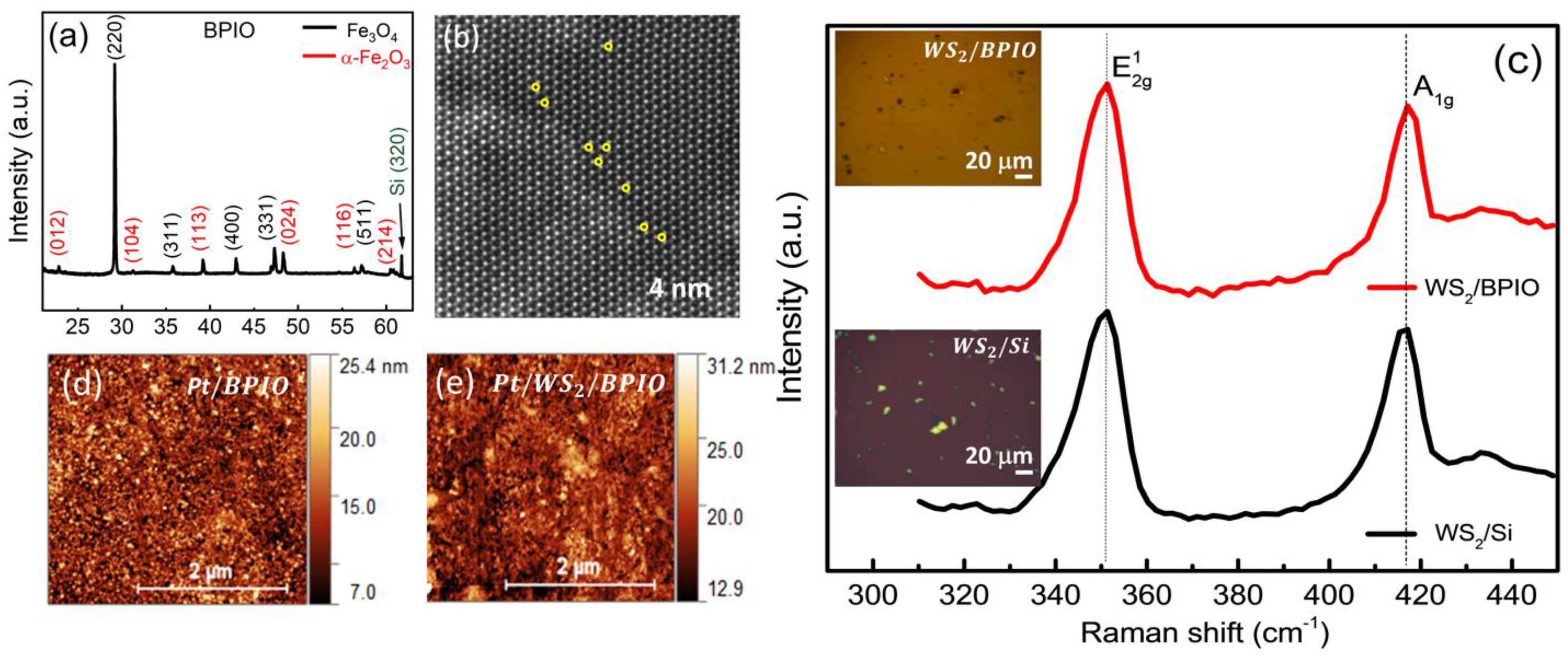
3.1. Material’s Characterization

To study the influence of the insertion of TMD monolayers on the physical properties of the HM/FM heterostructure, Pt/ML-WS2/BPIO and Pt/BPIO (the reference sample) were prepared (as detailed in Figure S1). WS2 flakes (monolayers) were wet transferred on top of a 20 nm thick BPIO film. Figure 1a represents the X-ray diffraction (XRD) pattern of our BPIO (20 nm)/Si film, confirming the coexistence of Fe3O4 and α-Fe2O3 phases. In addition, from the XRD data, the average crystallite size of Fe3O4 and α-Fe2O3 are estimated to be 115 nm and 55 nm, respectively, based on the Scherrer equation [46]. The coexistence of Fe3O4 and α-Fe2O3 phases is also confirmed by Raman spectroscopy as reported in our previous work [24]. High resolution scanning transmission electron microscopy (STEM) confirms the quality of the WS2 structure with some sulfur vacancies as seen in Figure 1b. The optical images in insets of Figure 1c show the WS2 flakes before and after transferring to the BPIO film. In addition, an estimation of WS2 flakes surface coverage is around 10.7%. The Raman spectra show two modes, E 2 g 1 (351 cm−1) and A1g (417 cm−1), of the WS2 flakes before (WS2 flakes/Si) and after transferring (WS2 flakes/BPIO), indicating a successful transfer process. A small bump (433 cm−1) next to A1g peak appears to occur due to the presence of S vacancies in WS2 [47], which is evident in the STEM image (Figure 1b). A 5 nm layer of Pt was deposited on both WS2/BPIO and BPIO films, forming Pt/WS2/BPIO and Pt/BPIO heterostructures. The surface topologies of the Pt/WS2/BPIO and Pt/BPIO films were characterized by atomic force microscopy (AFM), as shown in Figure 1d,e. The average surface roughness of Pt/WS2/BPIO and Pt/BPIO are determined to be ~3.388 nm and ~3.377 nm, respectively, indicating similar surface characteristics for both films.

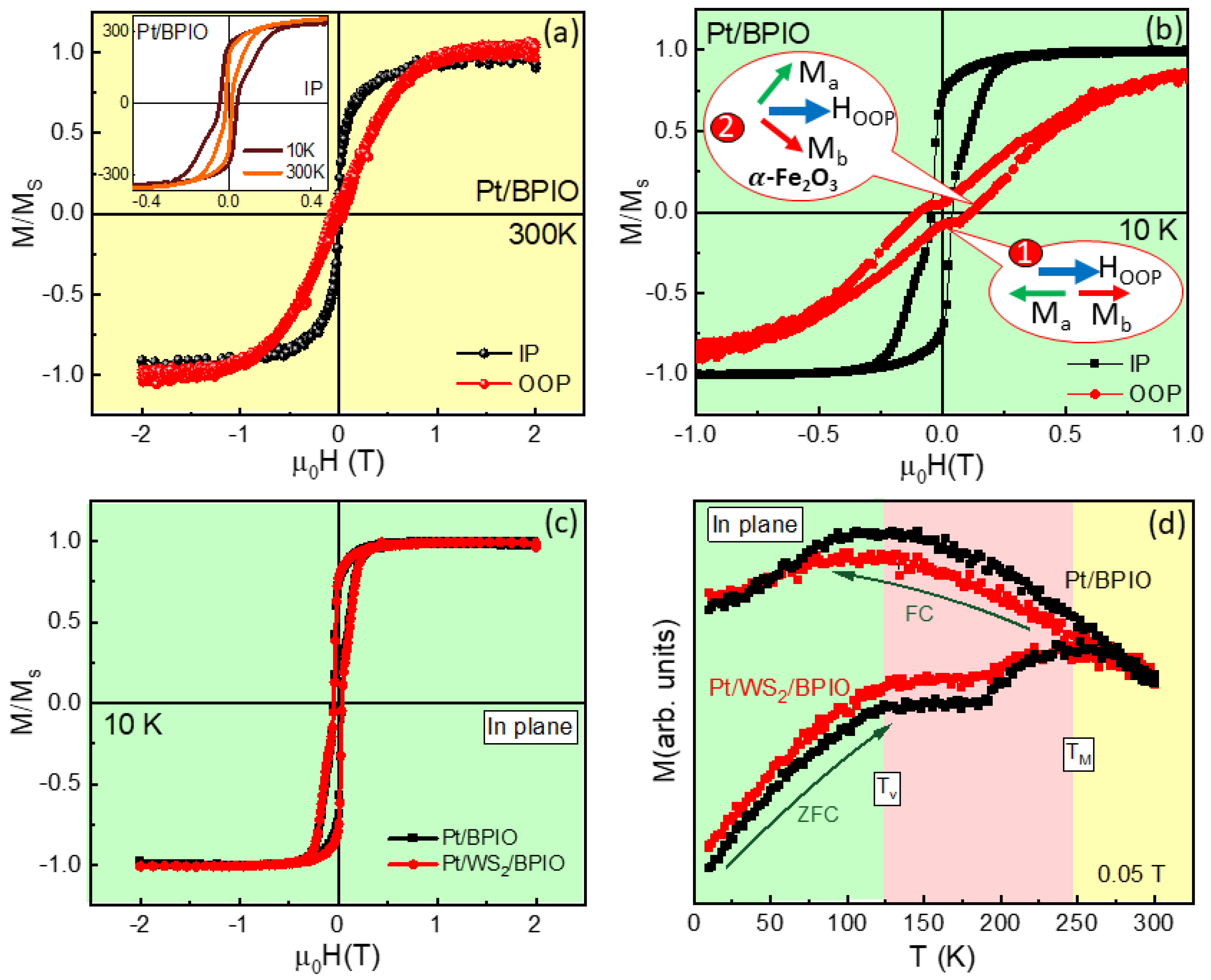
3.2. Magnetic Properties

The magnetic properties of the Pt/WS2/BPIO and Pt/BPIO films were then characterized using the vibrating sample magnetometer (VSM) equipped within a physical property measurement system (PPMS) from Quantum Design. Magnetization versus magnetic field (M-H) measurements were conducted on the Pt/BPIO film for both in-plane (IP) and out-of-plane (OOP) field directions. Figure 2a shows that BPIO possesses an IP easy axis at room temperature. As shown in the inset of Figure 2a, the IP M-H isotherms at 10 and 300 K clearly exhibit non-monotonic curves indicating bi-phase structures, as detected by the XRD. In addition, the coercive field (HC) is significantly enhanced as the temperature is lowered from 300 K to 10 K. The zoomed-in M-H curves for both IP and OOP M-H loops measured at 10 K are plotted in Figure 2b. Interestingly, a spin flop-like transition can be observed in the OOP M-H curve, likely due to the low field spin flop transition of the AFM α-Fe2O3 phase [37]. Since Fe3O4 is the dominant phase in the BPIO film, the spin flop-like behavior starts at an even lower field region, as compared to pure α-Fe2O3. When the magnetic field approaches zero, a plateau-like feature is observed, which can be attributed to the effect of the applied magnetic field which is insufficient to align the spin sublattices a and b in the α-Fe2O3 phase, and these two spin sublattices of α-Fe2O3 are anti-parallel to each other, as illustrated in inset #1 of Figure 2b. A gradual increase of the magnetic field reveals that the spin flop-like behavior occurs when the two sublattices rotate towards the magnetic field’s direction but do not fully align with it (inset #2 of Figure 2b). Because this spin flop-like behavior only occurs in the OOP measurement, it is reasonable to infer that the spin sublattice of α-Fe2O3 mostly lies in the OOP direction, and the Néel vector is in the IP direction. In Figure 2c, we compare the IP M-H curves for Pt/BPIO and Pt/WS2/BPIO at 10 K. The insertion of WS2 does not significantly alter the shape of the M-H hysteresis nor the saturation magnetization (MS). This can be reconciled to the fact that the induced magnetic moment in the WS2 layer is not detectable by the PPMS, which is also consistent with the small value of M obtained from DFT calculations. Figure 2c also indicates that the solvent clean process did not damage the BPIO surface and alter the nature of two phases after the wet transfer. Figure 2d shows zero field cooled (ZFC) and field cooled (FC) magnetization versus temperature (M-T) curves for both the films measured in a magnetic field of 0.05 T for the IP field direction. Upon cooling from room temperature, the ZFC M(T) first increases and shows a broad maximum around TM ~250 K and drops gradually down to 200 K. As the temperature goes down further, the ZFC M(T) shows a shoulder-like trend, and M starts dropping significantly around TV ~120 K toward the lowest temperature. The feature around TM ~250 K is associated with the Morin transition of the AFM α-Fe2O3 phase, while the feature at the TV originates from the Verwey transition of the Fe3O4 phase [24]. The relevant transition temperature regions have been highlighted below the TV (green), above the TV and below the TM (pink), and, above the TM (yellow). Overall, our XRD, Raman, and magnetometry data consistently show the coexistence of Fe3O4 and α-Fe2O3 phases in the BPIO film, and this feature is preserved in Pt/WS2/BPIO.

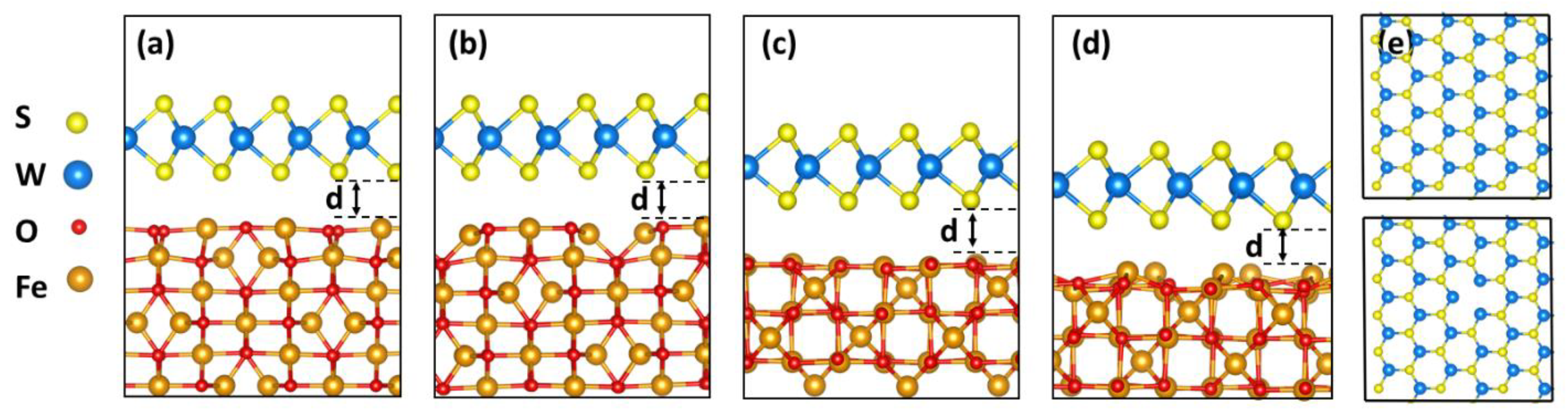
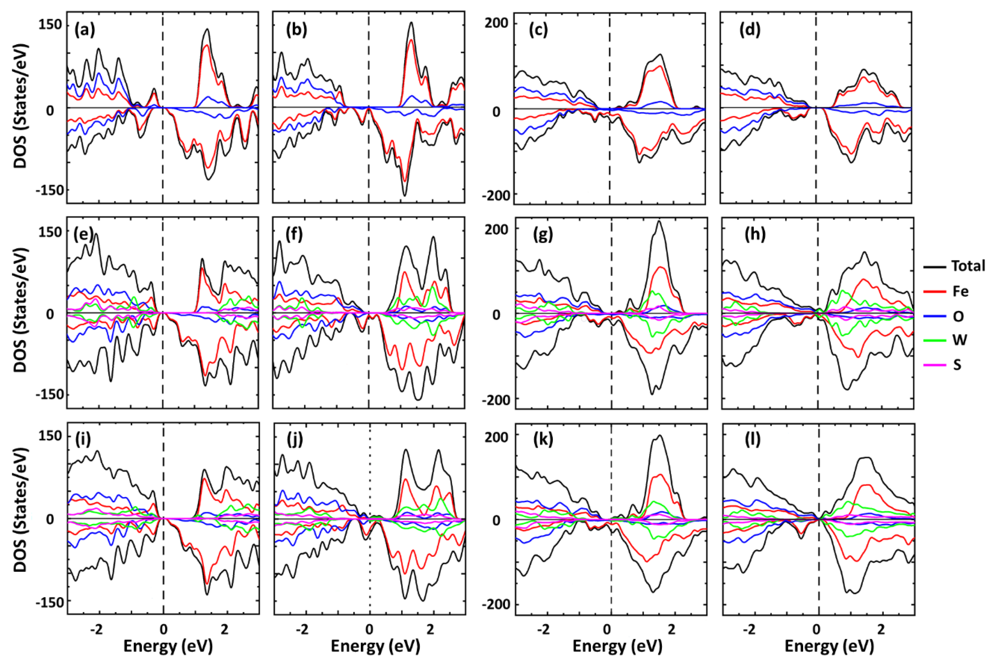
3.3. First Principles Calculations

Given that the Fe3O4 phase is predominant in the samples, we further investigate from first principles WS2/Fe3O4 heterostructures as a prototype of the magnetic interface properties of our experiments. The calculations are performed within DFT as implemented in the VASP code and relevant details are given in Methods. Despite the computational limitations due to the large number of atoms and the incommensurate lattices of the different components of the experimental heterostructures, we simulate several WS2/Fe3O4 heterostructures to discern between the low and high temperature phases of the magnetite. The supercells are constructed (details in Methods) by taking layers for the cubic and monoclinic phases with two types of (110) surfaces depending on the location of the surface Fe atoms. Given the polycrystalline nature of the presently studied BPIO film, different surface terminations of Fe3O4 are considered in our DFT calculations. These are given in Figure 3, where WS2 is placed above a B- and AB-terminated cubic Fe3O4 (Figure 3a,b, respectively), and B- and A-terminated monoclinic Fe3O4 (Figure 3c,d, respectively). In addition, pristine and defective WS2 monolayers containing 5 % S vacancies are also considered. The defective monolayer is obtained by removing two adjacent S atoms, as shown in Figure 3e. The magnetite contains six atomic layers (see Figure 3), and, during the simulations, the top two layers are allowed to relax while the remaining four are kept fixed at their bulk positions. Such a procedure enables capturing the unique role of the magnetite surface and its properties, as shown by others [44,45]. Due to the incommensurate lattices of WS2 and Fe3O4, the construction of the supercells and subsequent relaxation introduce slight strain, which does not exceed 5% for each component.
Results from the calculations for the interlayer distance, binding energy, and magnetic moments for the considered heterostructures are summarized in Table 1. We find that the interlayer distances d are smaller than typical van der Waals separations, which are usually ≥3 Å. On the other hand, the binding energies between WS2 and Fe3O4  E b ( 20 , 35 ) meV are consistent with weaker interactions indicative of van der Waals coupling [48]. The calculated average magnetic moments of the two inequivalent Fe (A and B) and the O atoms further show that the direction of the atomic spin polarization is preserved regardless of the WS2 presence. Not only that, the magnitude of m F e A , m F e B , and m O are not changed significantly for most considered heterostructures. This is a consequence of the rather small magnetization of WS2 above the magnetite, consistent with the experimental observations (Figure 2). This small magnetic proximity effect is not influenced significantly by the type of Fe3O4 surface termination, nor the presence of defects in the WS2 monolayer. The average magnetization of the WS2/Fe3O4 heterostructures is practically the same, with the exception of the A-terminated monoclinic magnetite layer for which an enhancement of M is found when compared to the standalone Fe3O4. It is interesting to note the increase in M cannot be attributed to the proximity magnetization of WS2 (since M W S 2 is insignificant), but it has a chemical origin due to orbital hybridization. These results show that the magnetic properties of the heterostructures are mainly determined by Fe3O4. The secondary role of WS2 is also in agreement with our measurements showing that the TMD does not significantly affect the magnetization properties of the heterostructure, as discussed above (also, see Figure 2).

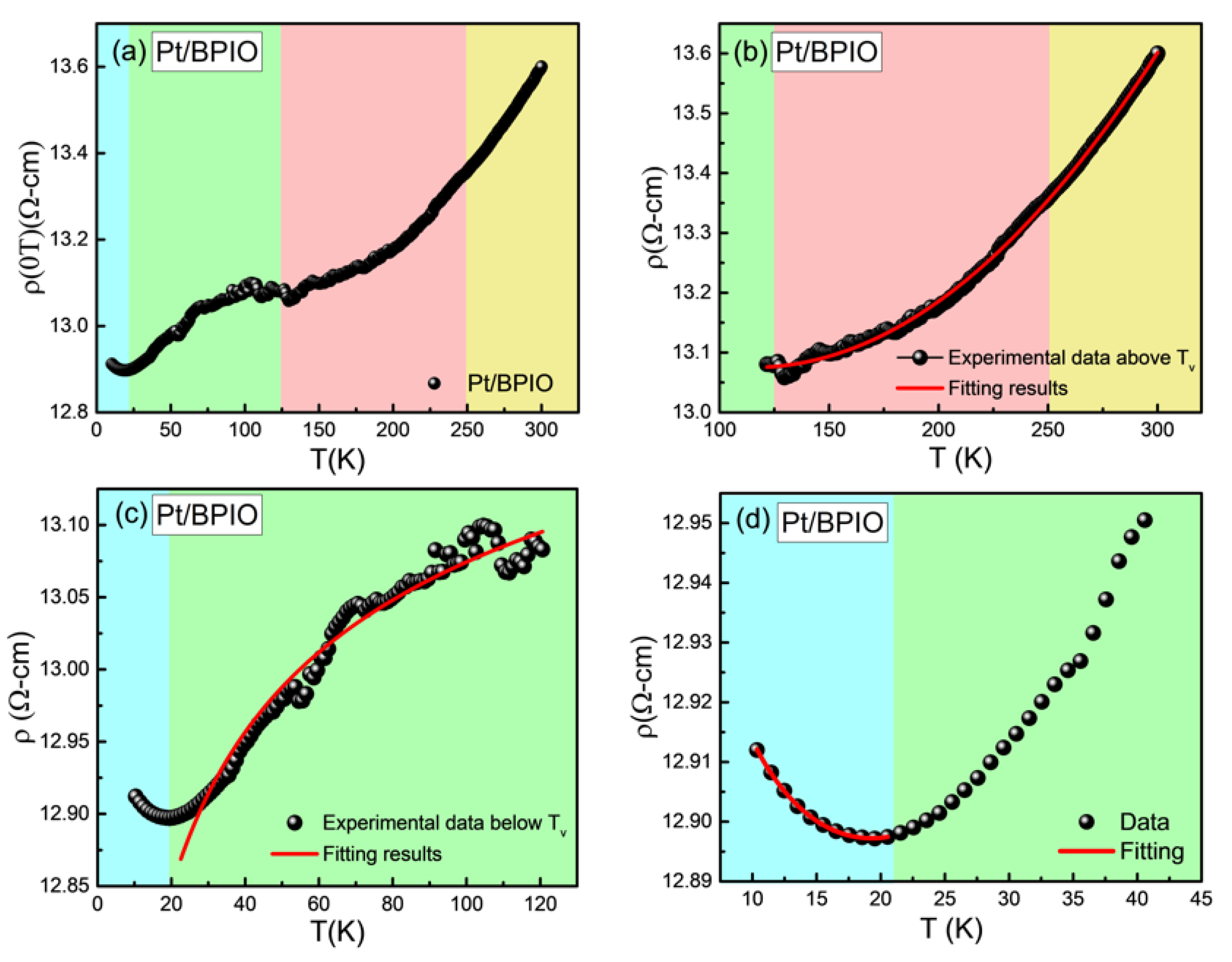
3.4. Four-Probe Measurement

To understand the effect of WS2 on the transport properties of the Pt/BPIO film, the temperature dependence of electrical resistivity ρ ( T ) was measured using a standard four-probe (FP) measurement technique in the absence of external magnetic field, as shown in Figure 4a. Interestingly, ρ ( T ) does not exhibit sharp changes around the two transition temperatures observed in our BPIO system, namely the Morin transition associated with the α-Fe2O3 phase and the Verwey transition associated with the Fe3O4 phase. This can be understood because the BPIO film is not epitaxial. The resistivity of this film around the TV does not increase as significantly as that grown on MgO [49]. The Verwey transition temperature can still be observed in the ρ ( T ) measurement. However, we cannot directly determine the transition temperature from the derivative of ρ ( T ) and broad maximum around the transition regions. This is because the BPIO system contains a biphase structure which could influence each other and broaden/shift the transition temperature. Above the TV, resistivity gradually increases without any significant slope change (Figure 4), as observed in the M-T curve (Figure 2). The absence of TM in ρ ( T ) is due to the small volume fraction of the α-Fe2O3 phase present in the BPIO film, and the consideration that the α-Fe2O3 phase is insulating throughout the measured temperature range. Chanda et al. [24] also found the absence of TM in the FP measurements. On the other hand, an additional transition temperature appears in the ρ ( T ) curve at a low temperature. To ascertain the origin of this low temperature behavior, different mechanisms for charge carrier conduction are discussed. Above the TV, while Fe3O4 has a half-metallic characteristic, we have a bi-phase structure for the presently studied sample, so the resistance state would be rather semiconducting than purely halfmetallic. The thermally activated behavior of resistivity governed by the Arrhenius model [50]
ρ ( T ) = ρ 0   e B T
can well describe the electrical transport mechanism for semiconducting and half-metallic materials, where B = E a / k B. Ea and k are activation energy and Boltzmann’s constant, respectively. The Arrhenius behavior for ρ ( T ) was reported before in Fe3O4 epitaxial films above the TV [51]. In addition, the ρ ( T ) for metallic Pt is fitted using the equation a + bT + cT2. Considering both layers (Pt and BPIO) as independent channels for charge transport with their resistances connected parallel to each other, the ρ ( T ) curve above the TV is fitted well with the expression:
ρ F e 3 O 4 P t = ρ F e 3 O 4 × ρ P t ρ F e 3 O 4 + ρ P t =   ( ρ 0   e B T ) × ( a + b T + c T 2 ) ( ρ 0   e B T ) + ( a + b T + c T 2 )
as shown in Figure 4b. Below the TV, variable range hopping (VRH) transport is the dominating mechanism for charge transport as the BPIO layer transforms to a semiconducting phase with higher resistance (where the Fe3O4 phase transforms from halfmetallic to semiconducting state with comparatively higher resistance [51], whereas the α-Fe2O3 phase remains insulating throughout the measured temperature range). In order to understand the nature of the VRH mechanism in the BPIO layer, we attempted to fit our ρ (T) data below the TV with both Mott’s 3D model [52],
ρ = A · e ( Q k T ) 1 4 ,
as well as Efros-Shklovskii (ES) model [53],
ρ = A · e ( Q k T ) 1 2 .
By comparing the Mott’s and ES fitting data, as indicated in Figure 4c, the best fit was obtained for Mott’s formula for a three-dimensional system [26]. However, the deviation from the VRH model below 40 K indicates the presence of additional mechanisms. Deviation from the VRH mechanism below ~60 K was observed before on an epitaxial Fe3O4 film [51]. Based on pure Pt’s temperature-dependent resistance (Figure S3), we confirm that neither Pt nor pure BPIO is responsible for the dip-like feature in ρ (T) since the resistivity for individual Pt and BPIO continuously decreases and increases with lowering temperature, respectively. To elucidate the low temperature electrical conduction mechanism, elastic electron-electron (e-e) scattering, and Kondo-like scattering are considered [54,55,56]. The former mechanism happens in inhomogeneous materials when temperature is low enough such that electrons experience a Coulomb interaction. Hence, the quantum correction causes the resistivity minimum [57,58]. The e-e interaction has a T1/2 contribution towards the resistivity. Kondo-like scattering is due to the magnetic impurities and therefore ln(T) behavior is expected [59]. In addition to the elastic scattering processes, the inelastic scattering due to electron-phonon (e-ph) and electron-magnon (e-m) scattering should also be considered. Since, in this case, the magnon propagation of Fe3O4 is short relative to the thickness of the sample [60], the e-m scattering channel is not relevant here. Therefore, resistivity can be corrected as:
ρ = ρ e l a s t i c + ρ i n e l a s t i c   ,
where ρ i n e l a s t i c ~T5 for e-ph scattering. The correction of the resistivity can be written as: ρ e l e l T1/2 + ρ e P h T5 for e-e interaction and ρ K l n ( T ) + ρ e P h   T 5 for Kondo-like scattering. However, two scenarios are fitted well as shown in the Figure S2. We combine the e-e scattering and Kondo-like scattering together as:
ρ = ρ 0 + ρ K l n ( T ) + ρ e l e l T 1 / 2 + ρ e p h   T 5 .
The result shown in Figure 4d indicates that the low temperature minimum, Tmin, behavior has contributions from both types of scattering. The reason for this behavior may originate from the diffusion of Fe into Pt causing magnetic impurities to become embedded inside Pt [33]. Since BPIO is more resistive at low temperatures, shunting current to the Pt layer could become more significant. As a result, the effect of a thin disordered interface could be more prominent at low temperatures. To compare the difference between Pt/BPIO and Pt/WS2/BPIO, the equation is also applied to Pt/WS2/BPIO. The fitting parameters are compared for both Pt/BPIO and Pt/WS2/BPIO. For Pt/BPIO, the parameters ρ 0 , ρ K , ρ e l e l , and ρ e p h are determined to be 13.04 ± 0.006, −0.132 ± 0.012, 0.0555 ± 0.007, and 7.234 × 10⁻¹⁰ ± 2.910 × 10⁻¹⁰, respectively. For Pt/WS2/BPIO, values of ρ 0 , ρ K , ρ e l e l , and ρ e p h are 15.145 ± 0.004, −0.148 ± 0.009, 0.059 ± 0.005, and 1.336 × 10⁻⁹ ± 1.840 × 10⁻¹⁰, respectively. These results indicate that in the temperature range around this minimum behavior in ρ ( T ) , Pt/WS2/BPIO has slightly stronger e-p scattering, with one order difference between these two systems. However, the e-e interaction and Kondo-like scattering do not have a significant difference. Interestingly, the local minimum behavior due to the interface interdiffusion did not manifest in the magnetic measurements. The main reason is that the dilute-magnetic semiconducting interface has much smaller magnetic signal compared to the magnetic property of bulk BPIO.

3.5. Atomically Resolved Spin Polarized Density of State

The phenomenological model discussed above is further enhanced by the calculated electronic structure of WS2/Fe3O4 heterostructures from first principles. In Figure 5, we show the results for the total and atomically resolved spin polarized DOS for the various systems. It is noted that the surface termination and structure phase are important for the electronic properties of the magnetite. Thus, letting the top two atomic layers relax, while the bottom four layers are kept fixed at their bulk positions (see Figure 3), is a practical way to capture the specific surface termination within a given structural phase of the magnetite [44,45]. We find that the cubic-B Fe3O4 is a ferromagnetic semiconductor (Figure 5a), while the cubic-AB termination increases the energy gap for spin “up” carriers, and spin “down” carriers exhibit halfmetallic behavior (Figure 5b). On the other hand, the monoclinic-B Fe3O4 is a half metal (Figure 5c) and the monoclinic-A Fe3O4 is a ferromagnetic semiconductor (Figure 5d). The proximity of the WS2 changes the DOS to various degrees. For example, Figure 5e shows that the WS2/Fe3O4 heterostructure is a semiconductor whose energy gaps for spin “up” and “down” are similar to the standalone cubic-B Fe3O4 layer. The presence of defects in WS2 does not alter this behavior. On the other hand, the spin “up” energy gap for the cubic-AB Fe3O4/WS2 is reduced when compared to the cubic-AB Fe3O4, and the defective WS2 monolayer turns the heterostructure in spin-polarized metal due to the non-zero DOS at the Fermi level (Figure 5f). The monoclinic-B Fe3O4/ WS2 exhibits similar behavior as the Fe3O4 (Figure 5g) and the defects in WS2 (Figure 5k) reduce the gap of the spin “up” carriers of the heterostructure when compared with the monoclinic-B Fe3O4 layer. Interestingly, the transition metal dichalcogenide results in a metallic DOS for both types of spin polarization of the monoclinic-A/Fe3O4 heterostructure, but the S vacancies lead to a reduction of DOS at the Fermi level (Figure 5l). Our calculations further show that in all cases, hybridization between the d -orbital of Fe and W occurs in the highest conduction and lowest valence ranges. The effect is the largest for the monoclinic-A Fe3O4/WS2 heterostructure, especially for d x 2 y 2 and d z 2 state from Fe and W in the Fermi level region. The semiconducting nature of the Fe3O4 found in the calculations can be correlated with the FP measurement that is fitted by the Arrhenius equation and VRH mechanism.

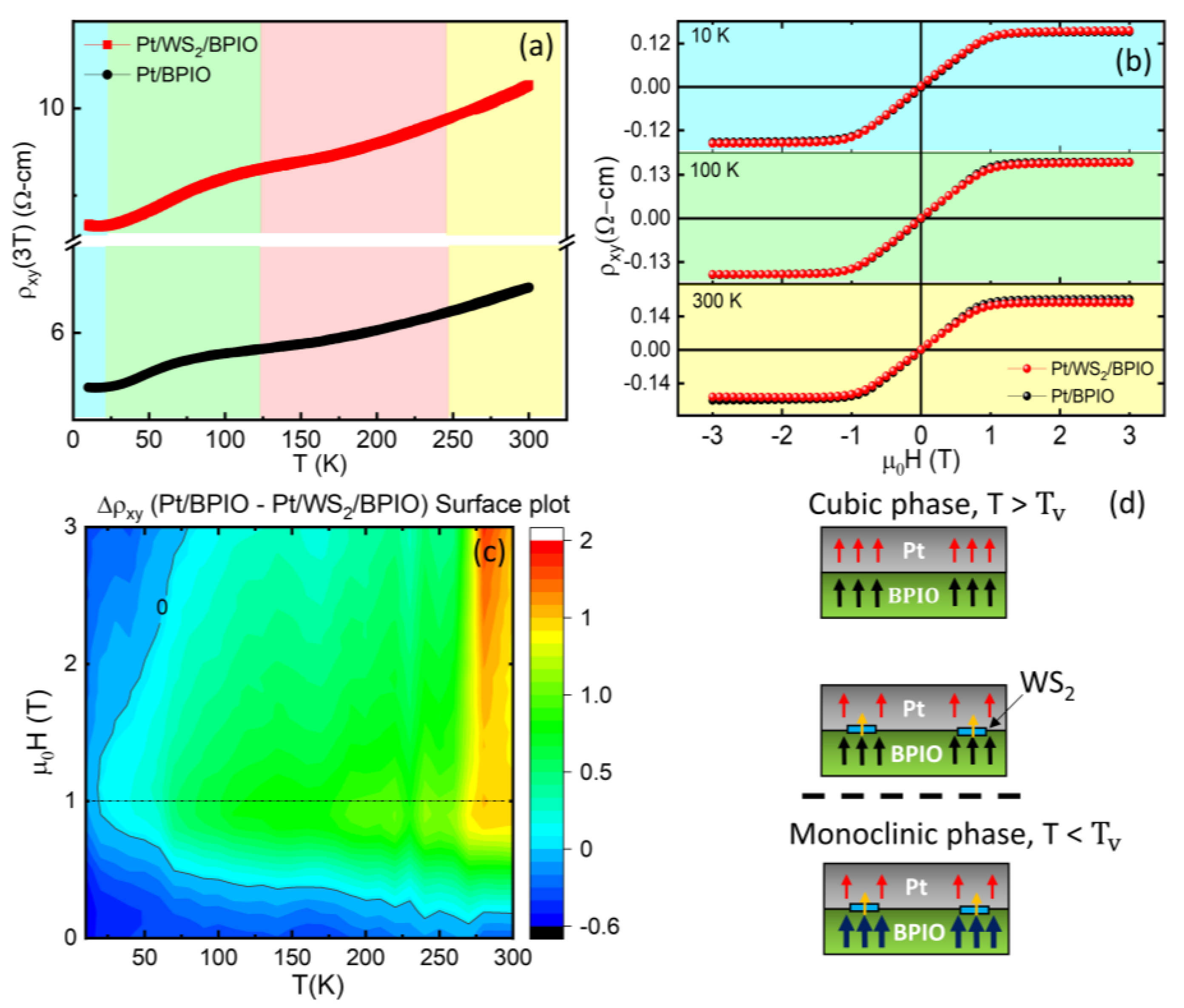
3.6. Anomalous Hall Effect Measurement

To further understand the interfacial effects, anomalous Hall effect (AHE) measurements were performed for Pt/BPIO and Pt/WS2/BPIO samples. When measuring resistivity of the films, the total resistivity is both contributed from ordinary Hall effect (OHE) and AHE. Hence, it can be written as:
ρ x y = R 0 H z + R S M z ,
where R0, Rs, Hz and Mz are the ordinary Hall coefficient, anomalous Hall coefficient, magnetic field along out of plane direction, and magnetization, respectively. The temperature dependence of ρxy at 3 T was measured, and a gradual decrease of ρxy(T) is observed (Figure 6a). Close to the saturating resistivity (ρsat) of the samples, the main contribution comes from AHE. When the temperature decreases, Fe3O4 becomes more and more insulating, hence the spin Hall Anomalous Hall resistivity (ρSH-AHE) is more dominant. The ρSH-AHE is dominated by the imaginary part of spin mixing conductance [61], which has a relatively small anomalous Hall signal compared to the traditional AHE. In the AHE measurement, TV and Tmin can still be observed in both the samples. However, for Tmin, both samples significantly reduce minimum point (14–16 K). This reason is possibly due to the application of a strong field (in this case, 3T), weakening the Kondo-like behavior. Figure 6b shows ρxy measured at three temperatures: 10, 100, and 300 K for Pt/BPIO and Pt/WS2/BPIO samples. When reaching ρsat, slightly larger ρxy for Pt/BPIO at 300 K is observed compared to Pt/WS2/BPIO. With continuously decreasing temperature, Pt/WS2/BPIO slightly increases ρxy and surpasses Pt/BPIO when temperature is below ~100 K. Figure 6c depicts the 2D surface plot of ρAHE difference between Pt/BPIO and Pt/WS2/BPIO. Around room temperature, the Pt/BPIO has significantly higher ρxy than Pt/WS2/BPIO (see Figure 6b). Pt and BPIO exhibit the MPE at high temperature since Pt is closer to a Stoner instability, which means that Pt is easier to induce magnetization. It has been reported in XMCD measurements that Pt and Fe-based complex oxides, such as Tm3Fe5O12, has a higher onset MPE temperature [62], and therefore Pt atomic layers close to the interface between Pt and BPIO can be easily proximitized (the top part of Figure 6d). However, Pt/WS2/BPIO has local WS2 flakes which increase the distance between Pt and BPIO and block the MPE between Fe3O4 and Pt (the middle panel of Figure 6d). Note here that we simply consider the MPE between Fe3O4 phase and Pt. Considering the high temperature Fe3O4 cubic phase, the calculations show that there is no enhancement in the magnetization, and rather, M is reduced in the cubic-AB/WS2 with defects in the TMD monolayer. The results of calculated high temperature cubic phase indicate not only WS2 blocks the MPE between Pt and Fe3O4 but also AB-cubic/WS2 with vacancy reduces the magnetization. Moreover, the AB-terminated cubic magnetite shows a halfmetallic behavior (Figure 5b–j) which explains the conducting nature above TV. As a result, Pt/BPIO has the higher magnetization compared to Pt/WS2/BPIO. At temperatures below TV, ρ x y shows slightly higher values in Pt/BPIO, which is opposite to the behavior above TV, and it is consistent with the negative values in the 2D surface plot. Connecting with the simulations, we see from Table 1, that the monoclinic-A/WS2 exhibits enhancement in the magnetization compared to the bare monoclinic-A case. Although the total M reduces after considering vacancy inside WS2, it still remains higher than the monoclinic-A one. Considering the B termination of the monoclinic phase, the magnetization enhances only after the insertion of vacancy. To further confirm the possibility of magnetization enhancement, we compare the results of DOS in Figure 5. Before any insertion of WS2, the B termination already has a halfmetallic behavior. However, A termination conveys a semiconducting property at monoclinic phase, similar to the case of low temperature Fe3O4 semiconducting/insulating behaviors. This explains the low temperature AHE enhancement behavior that is contributed from the monoclinic-A termination. The choice of the different surface terminations for the two temperature regimes (above and below the TV) can be reconciled with the polycrystalline characteristic of the BPIO film. According to the discussion above, the results of the magnetization enhancement can be attributed to the orbital hybridization between Fe3O4 and WS2, as shown in the bottom panel of Figure 6d. In order to distinguish the enhancement of the overall magnetization in the system, the BPIO magnetization in the monoclinic phase changes from the thinner black arrows towards the thicker dark blue arrows. In addition, the magnetization of Pt/WS2/BPIO enhances with further reducing temperature. It has been previously shown that in a MoS2/YIG system, valley polarization increases with lowering temperature [5]. This can be attributed to the suppression of thermal fluctuation with lowering temperature. In the low field region (<1T), Pt/WS2/BPIO has higher values of ρxy among all temperature regions of interest. Since OHE is inversely proportional to the carrier concentration [63], local WS2 flakes might lower the total carrier concentration owning to Pt being much more conductive. Consistent with the behavior of semiconducting materials, carrier concentration of WS2 drops with decreasing temperature. Therefore, the difference in the resistivity at low field increases with decreasing temperature. In addition, it is interesting to note that the Pt/WS2/BPIO magnetization is significantly enhanced with increasing field (>1T), which can be attributed to the change in spin alignment (from AFM to FM) within the Fe2O3 phase (Figure 2b), besides the Fe3O4 phase.

4. Conclusions

In conclusion, we have explored the properties of biphase BPIO (Fe3O4 + α-Fe2O3) and utilized the phase transitions in BPIO to probe the interfacial magnetic phenomena of 2D-TMD/FM heterostructures. From the experiments, the low temperature transition temperature found in the four-probe measurements was attributed to e-e scattering and Kondo-like behaviors based on the fitting results. A detailed analysis of the interfacial properties of Pt/WS2/BPIO shows the anomalous Hall resistivity enhancement at low temperatures, below the Verwey transition temperature. The enhancement of the resistivity in AHE measurements for Pt/WS2/BPIO comes from the orbital hybridization between the monoclinic-A Fe3O4 and WS2, which are confirmed by DFT calculations. In addition, the atomically resolved DOS shows the monoclinic-A terminated Fe3O4 interface with WS2 significantly changes the semiconducting behavior of the monoclinic-A Fe3O4 towards the metallic behavior, which can be attributed to the enhancement of the anomalous Hall resistivity. Both experiments and calculations confirm that the insertion of monolayer WS2 leads to the magnetization enhancement of the BPIO/WS2/Pt system. In future research, lower thicknesses of Fe3O4, as well as other conducting/insulating magnetic substrates may be used to fully explore and understand the MPE and spin transport across non-van der Waals magnet/van der Waals TMD interfaces. In addition to non-magnetic TMDs, magnetic TMD monolayers achieved recently via magnetic doping, also known as 2D diluted magnetic semiconductors [64,65], may be interfaced with non-van der Waals magnets to create heterostructures with optically controlled magnetic properties for opto-spin-caloritronics [4,66].

Supplementary Materials

The following supporting information can be downloaded at: https://www.mdpi.com/article/10.3390/nano13040771/s1, Figure S1: Schematic diagram of the wet transfer process; Figure S2: Low temperature resistivity behaviors for Pt/BPIO and Pt/WS2/BPIO. Figure S3: Temperature-dependent resistance measurement of pure Pt.

Author Contributions

Conceptualization, C.-M.H. and M.-H.P.; resource, N.A., M.L., D.Z. and M.T.; software, D.T.-X.D.; investigation, C.-M.H., D.T.-X.D., N.K., A.C., D.D., Y.T.H.P. and N.A.; formal analysis, C.-M.H. and D.T.-X.D.; data curation, C.-M.H.; writing—original draft preparation, C.-M.H. and D.T.-X.D.; writing—review and editing, A.C., H.R.G., D.A.A., S.W., L.M.W., H.S. and M.-H.P.; supervision, L.M.W. and M.-H.P.; project administration, L.M.W., H.S. and M.-H.P.; funding acquisition, H.S. and M.-H.P. All authors have read and agreed to the published version of the manuscript.

Funding

The research was funded by the US Department of Energy under Grant No. DE-FG02-07ER46438 and Grant No. DE-FG02-06ER46297, and by the NSF under Grant #ECCS-1952957.

Data Availability Statement

The research data will be available upon request.

Acknowledgments

H.S. and M.H.P. acknowledge financial support from the US Department of Energy, Office of Basic Energy Sciences, Division of Materials Science and Engineering under Grant No. DE-FG02-07ER46438. L.M.W. acknowledges financial support from the US Department of Energy under Grant No. DE-FG02-06ER46297. D.T.-X.D. would like to acknowledge support from the Presidential Fellowship sponsored by the University of South Florida. N.A. and D.A.A. acknowledge the support of the NSF under Grant #ECCS-1952957.

Conflicts of Interest

The authors declare no conflict of interest.

References

  1. Liu, Y.; Gao, Y.; Zhang, S.; He, J.; Yu, J.; Liu, Z. Valleytronics in Transition Metal Dichalcogenides Materials. Nano Res. 2019, 12, 2695–2711. [Google Scholar] [CrossRef]
  2. Liang, S.; Shi, S.; Hsu, C.H.; Cai, K.; Wang, Y.; He, P.; Wu, Y.; Pereira, V.M.; Yang, H. Spin-Orbit Torque Magnetization Switching in MoTe2/Permalloy Heterostructures. Adv. Mater. 2020, 32, 2002799. [Google Scholar] [CrossRef]
  3. Lee, W.Y.; Kang, M.S.; Kim, G.S.; Park, N.W.; Choi, K.Y.; Le, C.T.; Rashid, M.U.; Saitoh, E.; Kim, Y.S.; Lee, S.K. Role of Ferromagnetic Monolayer WSe2Flakes in the Pt/Y3Fe5O12Bilayer Structure in the Longitudinal Spin Seebeck Effect. ACS Appl. Mater. Interfaces 2021, 13, 15783–15790. [Google Scholar] [CrossRef] [PubMed]
  4. Phan, M.H.; Trinh, M.T.; Eggers, T.; Kalappattil, V.; Uchida, K.I.; Woods, L.M.; Terrones, M. A Perspective on Two-Dimensional van Der Waals Opto-Spin-Caloritronics. Appl. Phys. Lett. 2021, 119, 250501. [Google Scholar] [CrossRef]
  5. Tsai, S.P.; Yang, C.Y.; Lee, C.J.; Lu, L.S.; Liang, H.L.; Lin, J.X.; Yu, Y.H.; Chen, C.C.; Chung, T.K.; Kaun, C.C.; et al. Room-Temperature Ferromagnetism of Single-Layer MoS2 Induced by Antiferromagnetic Proximity of Yttrium Iron Garnet. Adv. Quantum Technol. 2021, 4, 2000104. [Google Scholar] [CrossRef]
  6. Lin, W.H.; Tseng, W.S.; Went, C.M.; Teague, M.L.; Rossman, G.R.; Atwater, H.A.; Yeh, N.C. Nearly 90% Circularly Polarized Emission in Monolayer WS2 Single Crystals by Chemical Vapor Deposition. ACS Nano 2020, 14, 1350–1359. [Google Scholar] [CrossRef] [PubMed] [Green Version]
  7. Li, Q.; Zhao, X.; Deng, L.; Shi, Z.; Liu, S.; Wei, Q.; Zhang, L.; Cheng, Y.; Zhang, L.; Lu, H.; et al. Enhanced Valley Zeeman Splitting in Fe-Doped Monolayer MoS2. ACS Nano 2020, 14, 4636–4645. [Google Scholar] [CrossRef] [Green Version]
  8. Lin, W.-H.; Wu, P.C.; Akbari, H.; Rossman, G.R.; Yeh, N.-C.; Atwater, H.A.; Lin, W.-H.; Akbari, H.; Atwater, H.A.; Wu, P.C.; et al. Electrically Tunable and Dramatically Enhanced Valley-Polarized Emission of Monolayer WS2 at Room Temperature with Plasmonic Archimedes Spiral Nanostructures. Adv. Mater. 2022, 34, 2104863. [Google Scholar] [CrossRef]
  9. Zhang, Y.; Shinokita, K.; Watanabe, K.; Taniguchi, T.; Goto, M.; Kan, D.; Shimakawa, Y.; Moritomo, Y.; Nishihara, T.; Miyauchi, Y.; et al. Controllable Magnetic Proximity Effect and Charge Transfer in 2D Semiconductor and Double-Layered Perovskite Manganese Oxide van Der Waals Heterostructure. Adv. Mater. 2020, 32, 2003501. [Google Scholar] [CrossRef]
  10. Zhang, W.; Zhang, L.; Wong, P.K.J.; Yuan, J.; Vinai, G.; Torelli, P.; van der Laan, G.; Feng, Y.P.; Wee, A.T.S. Magnetic Transition in Monolayer VSe2 via Interface Hybridization. ACS Nano 2019, 13, 8997–9004. [Google Scholar] [CrossRef]
  11. Messaoudi, O.; Ibañez-Azpiroz, J.; Bouzar, H.; Lounis, S. Nondegenerate Valleys in the Half-Metallic Ferromagnet Fe/WS2. Phys. Rev. B 2018, 97, 035404. [Google Scholar] [CrossRef] [Green Version]
  12. Zhang, F.; Mi, W.; Wang, X. Tunable Valley and Spin Splitting in 2 H -VSe2/BiFeO3(111) Triferroic Heterostructures. Nanoscale 2019, 11, 10329–10338. [Google Scholar] [CrossRef] [PubMed]
  13. Rossi, E.; Triola, C. Van Der Waals Heterostructures with Spin-Orbit Coupling. Ann. Der Phys. 2020, 532. [Google Scholar] [CrossRef] [Green Version]
  14. Zhou, H.; Chen, Y.; Zhu, H. Deciphering Asymmetric Charge Transfer at Transition Metal Dichalcogenide-Graphene Interface by Helicity-Resolved Ultrafast Spectroscopy. Sci. Adv. 2021, 7, eabg2999. [Google Scholar] [CrossRef] [PubMed]
  15. Manna, P.K.; Yusuf, S.M. Two Interface Effects: Exchange Bias and Magnetic Proximity. Phys. Rep. 2014, 535, 61–99. [Google Scholar] [CrossRef]
  16. Peng, B.; Li, Q.; Liang, X.; Song, P.; Li, J.; He, K.; Fu, D.; Li, Y.; Shen, C.; Wang, H.; et al. Valley Polarization of Trions and Magnetoresistance in Heterostructures of MoS2 and Yttrium Iron Garnet. ACS Nano 2017, 11, 12257–12265. [Google Scholar] [CrossRef]
  17. Hellman, F.; Hoffmann, A.; Tserkovnyak, Y.; Beach, G.S.D.; Fullerton, E.E.; Leighton, C.; Macdonald, A.H.; Ralph, D.C.; Arena, D.A.; Dürr, H.A.; et al. Interface-Induced Phenomena in Magnetism. Rev. Mod. Phys. 2017, 89, 025006. [Google Scholar] [CrossRef] [PubMed] [Green Version]
  18. Mendes, J.B.S.; Alves Santos, O.; Meireles, L.M.; Lacerda, R.G.; Vilela-Leão, L.H.; Machado, F.L.A.; Rodríguez-Suárez, R.L.; Azevedo, A.; Rezende, S.M. Spin-Current to Charge-Current Conversion and Magnetoresistance in a Hybrid Structure of Graphene and Yttrium Iron Garnet. Phys. Rev. Lett. 2015, 115, 226601. [Google Scholar] [CrossRef]
  19. Jie, W.; Yang, Z.; Zhang, F.; Bai, G.; Leung, C.W.; Hao, J. Observation of Room-Temperature Magnetoresistance in Monolayer MoS2 by Ferromagnetic Gating. ACS Nano 2017, 11, 6950–6958. [Google Scholar] [CrossRef]
  20. Lee, S.K.; Lee, W.Y.; Kikkawa, T.; Le, C.T.; Kang, M.S.; Kim, G.S.; Nguyen, A.D.; Kim, Y.S.; Park, N.W.; Saitoh, E. Enhanced Spin Seebeck Effect in Monolayer Tungsten Diselenide Due to Strong Spin Current Injection at Interface. Adv. Funct. Mater. 2020, 30, 2003192. [Google Scholar] [CrossRef]
  21. Thi-Xuan Dang, D.; Barik, R.K.; Phan, M.-H.; Woods, L.M. Enhanced Magnetism in Heterostructures with Transition-Metal Dichalcogenide Monolayers. J. Phys. Chem. Lett. 2022, 13, 8879–8887. [Google Scholar] [CrossRef]
  22. Norden, T.; Zhao, C.; Zhang, P.; Sabirianov, R.; Petrou, A.; Zeng, H. Giant Valley Splitting in Monolayer WS2 by Magnetic Proximity Effect. Nat. Commun. 2019, 10, 1–10. [Google Scholar] [CrossRef] [PubMed] [Green Version]
  23. Dai, J.Q.; Wang, X.W.; Cao, T.F. Large Band Offset in Monolayer MoS 2 on Oppositely Polarized BiFeO 3 (0001) Polar Surfaces. J. Phys. Chem. C 2019, 123, 3039–3047. [Google Scholar] [CrossRef]
  24. Chanda, A.; DeTellem, D.; Hai Pham, Y.T.; Shoup, J.E.; Duong, A.T.; Das, R.; Cho, S.; Voronine, D.V.; Trinh, M.T.; Arena, D.A.; et al. Spin Seebeck Effect in Iron Oxide Thin Films: Effects of Phase Transition, Phase Coexistence, And Surface Magnetism. ACS Appl. Mater. Interfaces 2022, 14, 13468–13479. [Google Scholar] [CrossRef]
  25. Kukreja, R.; Hua, N.; Ruby, J.; Barbour, A.; Hu, W.; Mazzoli, C.; Wilkins, S.; Fullerton, E.E.; Shpyrko, O.G. Orbital Domain Dynamics in Magnetite below the Verwey Transition. Phys. Rev. Lett. 2018, 121, 177601. [Google Scholar] [CrossRef] [Green Version]
  26. Lenge, N.; Kronmuller, H.; Walz, F. The Relation between Electrical Conductivity Mechanisms and Magnetic After-Effects in Single Crystal Magnetite. J. Phys. Soc. Jpn. 1984, 53, 1406–1414. [Google Scholar] [CrossRef]
  27. Yasui, S.; Honda, S.; Okabayashi, J.; Yanase, T.; Shimada, T.; Nagahama, T. Large Inverse Tunnel Magnetoresistance in Magnetic Tunnel Junctions with an Fe3 O4 Electrode. Phys. Rev. Appl. 2021, 15, 034042. [Google Scholar] [CrossRef]
  28. Wu, H.C.; Coileáin, C.; Abid, M.; Mauit, O.; Syrlybekov, A.; Khalid, A.; Xu, H.; Gatensby, R.; Jing Wang, J.; Liu, H.; et al. Spin-Dependent Transport Properties of Fe3O4/MoS2/Fe3O4 Junctions. Sci. Rep. 2015, 5, 15984. [Google Scholar] [CrossRef] [PubMed] [Green Version]
  29. Hirohata, A.; Yamada, K.; Nakatani, Y.; Prejbeanu, L.; Diény, B.; Pirro, P.; Hillebrands, B. Review on Spintronics: Principles and Device Applications. J. Magn. Magn. Mater. 2020, 509, 166711. [Google Scholar] [CrossRef]
  30. Fernández-Pacheco, A.; de Teresa, J.M.; Orna, J.; Morellon, L.; Algarabel, P.A.; Pardo, J.A.; Ibarra, M.R.; Magen, C.; Snoeck, E. Giant Planar Hall Effect in Epitaxial Fe3O4 Thin Films and Its Temperature Dependence. Phys. Rev. B-Condens. Matter Mater. Phys. 2008, 78, 212402. [Google Scholar] [CrossRef]
  31. Fernández-Pacheco, A.; de Teresa, J.M.; Orna, J.; Morellon, L.; Algarabel, P.A.; Pardo, J.A.; Ibarra, M.R. Universal Scaling of the Anomalous Hall Effect in Fe3O4 Epitaxial Thin Films. Phys. Rev. B-Condens. Matter Mater. Phys. 2008, 77, 100403. [Google Scholar] [CrossRef]
  32. Gridin, V.V.; Hearne, G.R.; Honig, J.M. Magnetoresistance Extremum at the First-Order Verwey Transition in Magnetite Fe3O4. Phys. Rev. B 1996, 53, 15518. [Google Scholar] [CrossRef] [PubMed]
  33. Genuzio, F.; Sala, A.; Schmidt, T.; Menzel, D.; Freund, H.J. Interconversion of α-Fe2O3 and Fe3O4 Thin Films: Mechanisms, Morphology, and Evidence for Unexpected Substrate Participation. J. Phys. Chem. C 2014, 118, 29068–29076. [Google Scholar] [CrossRef]
  34. Attanayake, S.B.; Chanda, A.; Das, R.; Phan, M.H.; Srikanth, H. Emergent Magnetic Properties of Biphase Iron Oxide Nanorods. AIP Adv. 2022, 12, 035136. [Google Scholar] [CrossRef]
  35. Cao, D.; Li, H.; Pan, L.; Li, J.; Wang, X.; Jing, P.; Cheng, X.; Wang, W.; Wang, J.; Liu, Q. High Saturation Magnetization of γ-Fe2O3 Nano-Particles by a Facile One-Step Synthesis Approach. Sci. Rep. 2016, 6, 1–9. [Google Scholar] [CrossRef] [Green Version]
  36. Tuček, J.; Zbořil, R.; Namai, A.; Ohkoshi, S.I. ε-Fe2O3: An Advanced Nanomaterial Exhibiting Giant Coercive Field, Millimeter-Wave Ferromagnetic Resonance, and Magnetoelectric Coupling. Chem. Mater. 2010, 22, 6483–6505. [Google Scholar] [CrossRef]
  37. Zhang, P.; Chou, C.-T.; Yun, H.; Mcgoldrick, B.C.; Hou, J.T.; Mkhoyan, K.A.; Liu, L. Control of Néel Vector with Spin-Orbit Torques in an Antiferromagnetic Insulator with Tilted Easy Plane. Phys. Rev. Lett. 2022, 129, 017203. [Google Scholar] [CrossRef]
  38. Kresse, G.; Furthmüller, J. Efficiency of Ab-Initio Total Energy Calculations for Metals and Semiconductors Using a Plane-Wave Basis Set. Comput. Mater. Sci. 1996, 6, 15–50. [Google Scholar] [CrossRef]
  39. Kresse, G.; Furthmüller, J. Efficient Iterative Schemes for Ab Initio Total-Energy Calculations Using a Plane-Wave Basis Set. Phys. Rev. B 1996, 54, 11169. [Google Scholar] [CrossRef]
  40. Kresse, G.; Joubert, D. From Ultrasoft Pseudopotentials to the Projector Augmented-Wave Method. Phys. Rev. B 1999, 59, 1758. [Google Scholar] [CrossRef]
  41. Chanda, A.; Hung, C.M.; Duong, A.T.; Cho, S.; Srikanth, H.; Phan, M.H. Magnetism and Spin-Dependent Transport Phenomena across Verwey and Morin Transitions in Iron Oxide/Pt Bilayers. J. Magn. Magn. Mater. 2023, 568, 170370. [Google Scholar] [CrossRef]
  42. Grimme, S. Density Functional Theory with London Dispersion Corrections. Ltd. WIREs Comput Mol Sci 2011, 1, 211–228. [Google Scholar] [CrossRef]
  43. Jeng, H.T.; Guo, G.Y.; Huang, D.J. Charge-Orbital Ordering in Low-Temperature Structures of Magnetite: GGA + U Investigations. Phys. Rev. B-Condens. Matter Mater. Phys. 2006, 74, 195115. [Google Scholar] [CrossRef] [Green Version]
  44. Yu, X.; Huo, C.F.; Li, Y.W.; Wang, J.; Jiao, H. Fe3O4 Surface Electronic Structures and Stability from GGA + U. Surf. Sci. 2012, 606, 872–879. [Google Scholar] [CrossRef]
  45. Li, Y.L.; Yao, K.L.; Liu, Z.L. First-Principle Studies on the Electronic Structure of Fe3O4(110) Surface. Front. Phys. China 2007, 2, 76–80. [Google Scholar] [CrossRef]
  46. Ingham, B.; Toney, M.F. X-Ray Diffraction for Characterizing Metallic Films. In Metallic Films for Electronic, Optical and Magnetic Applications; Woodhead Publishing: Sawston, UK, 2014; pp. 3–38. [Google Scholar] [CrossRef]
  47. Lee, C.; Jeong, B.G.; Yun, S.J.; Lee, Y.H.; Lee, S.M.; Jeong, M.S. Unveiling Defect-Related Raman Mode of Monolayer WS2 via Tip-Enhanced Resonance Raman Scattering. ACS Nano 2018, 12, 9982–9990. [Google Scholar] [CrossRef]
  48. Pollard, T.D.; Thomas, D.; Earnshaw, W.C.; Lippincott-Schwartz, J.; Johnson, G.T. Cell Biology, 3rd ed.; Elsevier: Philadelphia, PA, USA, 2017. [Google Scholar]
  49. Liu, X.H.; Rata, A.D.; Chang, C.F.; Komarek, A.C.; Tjeng, L.H. Verwey Transition in Fe3O4 Thin Films: Influence of Oxygen Stoichiometry and Substrate-Induced Microstructure. Phys. Rev. B 2014, 90, 125142. [Google Scholar] [CrossRef] [Green Version]
  50. Lin, T.T.; Young, S.L.; Kung, C.Y.; Chen, H.Z.; Kao, M.C.; Chang, M.C.; Ou, C.R. Variable-Range Hopping and Thermal Activation Conduction of y-Doped ZnO Nanocrystalline Films. IEEE Trans. Nanotechnol. 2014, 13, 425–430. [Google Scholar] [CrossRef] [Green Version]
  51. Ramos, R.; Arora, S.K.; Shvets, I. Anomalous Anisotropic Magnetoresistance in Epitaxial Fe3O4 Thin Films on MgO(001). Phys. Rev. B 2008, 78, 214402. [Google Scholar] [CrossRef] [Green Version]
  52. Mott, N.F.; Davis, E.A. Electronic Processes in Non-Crystalline Materials; Oxford University Press: Oxford, UK, 2012. [Google Scholar]
  53. Shklovskii, B.I.; Efros, A.L. Electronic Properties of Doped Semiconductors; Springer Science & Business Media: Berlin/Heidelberg, Germany, 2013; Volume 45. [Google Scholar]
  54. De, K.; Das, S. Low-temperature localization in the transport properties of self-doped La0.9Mn0.98Zn0.02O3. Bull. Mater. Sci. 2010, 39, 293–298. [Google Scholar] [CrossRef] [Green Version]
  55. Cirillo, C.; Barone, C.; Bradshaw, H.; Urban, F.; di Bernardo, A.; Mauro, C.; Robinson, J.W.A.; Pagano, S.; Attanasio, C. Magnetotransport and Magnetic Properties of Amorphous NdNi 5 Thin Films. Sci. Rep. 2020, 10, 13693. [Google Scholar] [CrossRef]
  56. Shiomi, Y.; Ohtani, T.; Iguchi, S.; Sasaki, T.; Qiu, Z.; Nakayama, H.; Uchida, K.; Saitoh, E. Interface-Dependent Magnetotransport Properties for Thin Pt Films on Ferrimagnetic Y3Fe5O12. Appl. Phys. Lett. 2014, 104, 242406. [Google Scholar] [CrossRef] [Green Version]
  57. Lee, P.A.; Ramakrishnan, T.V. Disordered Electronic Systems. Rev. Mod. Phys. 1985, 57, 287. [Google Scholar] [CrossRef]
  58. Pollak, A.L.E.M. Electron-Electron Interactions in Disordered Systems, 1st ed.; Elsevier: Amsterdam, The Netherlands, 2015; Volume 10. [Google Scholar]
  59. Kondo, J. Resistance Minimum in Dilute Magnetic Alloys. Prog. Theor. Phys. 1964, 32, 37–49. [Google Scholar] [CrossRef] [Green Version]
  60. Venkat, G.; Cox, C.D.W.; Voneshen, D.; Caruana, A.J.; Piovano, A.; Cropper, M.D.; Morrison, K. Magnon Diffusion Lengths in Bulk and Thin Film Fe3O4 for Spin Seebeck Applications. arXiv 2020, arXiv:2001.03738. [Google Scholar] [CrossRef]
  61. Chen, Y.-T.; Takahashi, S.; Nakayama, H.; Althammer, M.; Goennenwein, S.T.B.; Saitoh, E.; Bauer, G.E.W. Theory of Spin Hall Magnetoresistance. Phys. Rev. B 2013, 87, 144411. [Google Scholar] [CrossRef] [Green Version]
  62. Shao, Q.; Grutter, A.; Liu, Y.; Yu, G.; Yang, C.Y.; Gilbert, D.A.; Arenholz, E.; Shafer, P.; Che, X.; Tang, C.; et al. Exploring Interfacial Exchange Coupling and Sublattice Effect in Heavy Metal/Ferrimagnetic Insulator Heterostructures Using Hall Measurements, X-ray Magnetic Circular Dichroism, and Neutron Reflectometry. Phys. Rev. B 2019, 99, 104401. [Google Scholar] [CrossRef] [Green Version]
  63. Toyosaki, H.; Fukumura, T.; Yamada, Y.; Nakajima, K.; Chikyow, T.; Hasegawa, T.; Koinuma, H.; Kawasaki, M. Anomalous Hall Effect Governed by Electron Doping in a Room-Temperature Transparent Ferromagnetic Semiconductor. Nat. Mater. 2004, 3, 221–224. [Google Scholar] [CrossRef] [PubMed]
  64. Pham, Y.T.H.; Liu, M.; Jimenez, V.O.; Yu, Z.; Kalappattil, V.; Zhang, F.; Wang, K.; Williams, T.; Terrones, M.; Phan, M.H. Tunable Ferromagnetism and Thermally Induced Spin Flip in Vanadium-Doped Tungsten Diselenide Monolayers at Room Temperature. Adv. Mater. 2020, 32, 2003607. [Google Scholar] [CrossRef] [PubMed]
  65. Zhang, F.; Zheng, B.; Sebastian, A.; Olson, D.H.; Liu, M.; Fujisawa, K.; Thi Hai Pham, Y.; Ortiz Jimenez, V.; Kalappattil, V.; Miao, L.; et al. COMMUNICATION Monolayer Vanadium-Doped Tungsten Disulfide: A Room-Temperature Dilute Magnetic Semiconductor. Adv. Sci. 2020, 7, 2001174. [Google Scholar] [CrossRef] [PubMed]
  66. Ortiz Jimenez, V.; Pham, Y.T.H.; Liu, M.; Zhang, F.; Yu, Z.; Kalappattil, V.; Muchharla, B.; Eggers, T.; Duong, D.L.; Terrones, M.; et al. Light-Controlled Room Temperature Ferromagnetism in Vanadium-Doped Tungsten Disulfide Semiconducting Monolayers. Adv. Electron. Mater. 2021, 7, 2100030. [Google Scholar] [CrossRef]
Figure 1. (a) X−ray diffraction (XRD) pattern for the 20 nm thick BPIO film. (b) WS2 flakes under high resolution scanning transmission electron microscopy (STEM). The yellow circles indicate S vacancies in WS2. (c) Raman spectra for WS2 flakes before (WS2/Si) and after (WS2/BPIO) the wet transfer process. Atomic force microscopy (AFM) was performed after Pt deposition for (d) Pt/BPIO and (e) Pt/WS2/BPIO. Insets of (b) indicate the optical images of WS2 flakes on Si (before the transfer process) and BPIO (after the transfer process), respectively.
Nanomaterials 13 00771 g001
Figure 2. M−H curves are measured for (a) Pt/BPIO at 300 K in IP and OOP directions and (b) Pt/BPIO under low field at 10K in the IP direction. (c) IP M−H curves for Pt/BPIO and Pt/WS2/BPIO at 10 K. (d) M-T curves for both Pt/BPIO and Pt/WS2/BPIO for the IP direction. Inset of (a) has Pt/BPIO measured at 10 and 300 K for IP magnetic field. Inset of (b) indicates the α−Fe2O3 spin flop transition behaviors. Ma (green) and Mb (red) are two sublattices for α−Fe2O3. OOP magnetic field is noted as blue arrow.
Nanomaterials 13 00771 g002
Figure 3. Side view of the simulated Fe3O4 (110)/WS2 heterostructures: (a) B-terminated cubic Fe3O4; (b) AB-terminated cubic Fe3O4; (c) B-terminated monoclinic Fe3O4; (d) A-terminated monoclinic Fe3O4. (e) Top view of WS2 and WS2 (VS-S) with two adjacent S vacancies.
Nanomaterials 13 00771 g003
Figure 4. Zero field resistivity measured at temperatures between 10 and 300 K for (a) Pt/BPIO. Curves fitted for temperatures (b) above and (c) below the TV in Pt/BPIO and (d) the minimum resistivity behavior noted below 20 K.
Nanomaterials 13 00771 g004
Figure 5. Total and atomically resolved density of states for a standalone Fe3O4 layer: (a) cubic−B, (b) cubic−AB, (c) monoclinic−B, (d) monoclinic−A Fe3O4 layer; and for Fe3O4/WS2 heterostructures: (e) cubic−B/WS2, (f) cubic−AB/WS2, (g) monoclinic−B/WS2, (h) monoclinic−A/WS2, (i) cubic−B/WS2 (VS-S), (j) cubic−AB/WS2 (VS-S), (k) monoclinic−B/WS2 (VS−S), (l) monoclinic−A/WS2 (VS−S). In all cases, the top two atomic layers of Fe3O4 are allowed to relax, while the bottom four layers are kept at their bulk positions (see Section 2).
Nanomaterials 13 00771 g005
Figure 6. AHE measurements for Pt/BPIO and Pt/WS2/BPIO: (a) temperature−dependent ρxy at 3 T and (b) ρxy at selected temperatures of 10, 100, and 300 K. (c) 2D surface plot of the ρxy difference between Pt/BPIO and Pt/WS2/BPIO. (d) Schematics showing possible differences in MPE between different Fe3O4 phases (cubic and monoclinic) and Pt, as well as the insertion of WS2. Red, black, and yellow arrows indicate Pt, WS2, and BPIO magnetization, respectively.
Nanomaterials 13 00771 g006
Table 1. Basic properties of the considered heterostructures and standalone Fe3O4 layers with cubic-B, cubic-AB, monoclinic-B, and monoclinic-B surface terminations. The interlayer distance d (Å), binding energy E b = ( E H S T i E i l a y e r ) / N ( E H S T is the total energy of the heterostructure, E i l a y e r is the total energy of the ith isolated layer, N is the number of atoms in the supercell), average magnetic moments for the inequivalent atoms of Fe3O4  m F e A ,   m F e B ,   m O , the total magnetization per atom of the WS2 monolayer M W S 2 , and total magnetization per atom of the entire structure M (all magnetic properties are in ( μ B ) units) are shown.
Interlayer
Distance d (Å)
Binding   Energy   E b ( meV ) m F e A  
( μ B )
m F e B  
( μ B )
m O  
( μ B )
M W S 2  
( μ B )
M  
( μ B )
Cubic-B--−3.8653.9830.118-0.667
Cubic-B/WS22.521−21.967−3.8623.9880.1140.0030.667
Cubic-B/WS2 (VS-S)2.505−22.981−3.8623.9860.1150.0030.667
Cubic-AB--−3.8753.9830.118-0.667
Cubic-AB/WS22.642−34.880−3.8713.9940.1120.0060.667
Cubic-AB/WS2 (VS-S)2.537−35.288−3.8694.0000.1130.0030.666
Monoclinic-B--−3.9074.0070.139-0.667
Monoclinic-B/WS22.822−20.322−3.8863.9920.1340.0030.667
Monoclinic-B/WS2 (VS-S)2.780−17.715−3.8873.9970.1360.0020.668
Monoclinic-A--−3.8873.9710.129-0.667
Monoclinic-A/WS22.207−30.058−3.8743.9770.1320.000060.672
Monoclinic-A/WS2 (VS-S)1.958−27.378−3.8673.9860.127−0.0010.671
Disclaimer/Publisher’s Note: The statements, opinions and data contained in all publications are solely those of the individual author(s) and contributor(s) and not of MDPI and/or the editor(s). MDPI and/or the editor(s) disclaim responsibility for any injury to people or property resulting from any ideas, methods, instructions or products referred to in the content.

