

High-Sensitivity Sensing in All-Dielectric Metasurface Driven by Quasi-Bound States in the Continuum

1
Computer Science and Information Engineering School, Xiamen Institute of Technology, Xiamen 361021, China
2
College of Information Science and Engineering, Huaqiao University, Xiamen 361021, China
*
Author to whom correspondence should be addressed.
Nanomaterials 2023, 13(3), 505; https://doi.org/10.3390/nano13030505
Submission received: 30 December 2022
/
Revised: 15 January 2023
/
Accepted: 19 January 2023
/
Published: 27 January 2023
(This article belongs to the Topic Advanced Nanomaterials for Sensing Applications)
Abstract
:Quasi-bound states in the continuum (quasi-BIC) in all-dielectric metasurfaces provide a crucial platform for sensing due to its ability to enhance strong matter interactions between light-waves and analytes. In this study, a novel high-sensitivity all-dielectric sensor composed of a periodic array of silicon (Si) plates with square nanoholes in the continuous near-infrared band is theoretically proposed. By adjusting the position of the square nanohole, the symmetry-protected BIC and Friedrich–Wintgen BIC (FW–BIC) can be excited. The torodial dipole (TD) and electric quadruple (EQ) are demonstrated to play a dominating role in the resonant modes by near-field analysis and multipole decomposition. The results show that the sensitivity, the Q-factor, and the corresponding figure of merit (FOM) can simultaneously reach 399 nm/RIU (RIU is refractive index unit), 4959, and 1281, respectively. Compared with other complex nanostructures, the proposed metasurface is more feasible and practical, which may open up an avenue for the development of ultrasensitive sensors.
1. Introduction
Metasurface is an artificially arranged array of periodic subwavelength structures with unusual electromagnetic characteristics, such as negative refractive index [1], near-zero refractive index [2], and negative magnetic permeability [3]. With the development of micro-nano processing technology, metasurfaces are widely used in metalens [4], light absorbers [5], biochemical sensors [6], and optical modulators [7]. Compared with three-dimensional (3-D) structures, photonic crystals, or metal resonators, dielectric supersurfaces with high Q-factor have advantages in terms of flexibility, size, and nonlinear optical compatibility [8,9,10]. The all-dielectric metasurface supports Mie resonance and can provide high Q-factor and FOM (Figure of Merit), and is more compatible with complementary metal oxide semiconductor production processes [10,11,12]. Therefore, all-dielectric metasurface-based sensors exhibit stronger light-harvesting capabilities and smaller volumes, enabling label-free, on-chip integration, and ultrasensitive sensing, which become current research hotspots. In 2020, Jeeyoon et al. presented a metasurface structure composed of an all-dielectric hollow cuboid array, which can be used for refractive index sensing with a maximum sensitivity of 161 nm/RIU and a FOM of 78 [13]. In 2021, Zhang et al. suggested a “lucky junction”-shaped all-dielectric nanostructure that is insensitive to polarization and incident angle, with a sensitivity of 986 nm/RIU and a FOM of 32.7 [14]. In 2022, Song et al. proposed a refractive index sensor composed of two asymmetric rectangular hollow silicon cylinders, with a maximum sensitivity of 160 nm/RIU and a FOM of 575 [15].
The idea of bound states in the continuum (BIC) has been included into various metasurface designs in order to achieve higher Q resonances [16,17,18,19,20,21]. BIC designates a state that still preserves locality in the continuous domain, which can be explained by destructive interference. The coupling of the BIC resonant mode to all radiated waves vanishes when the system parameters are continuously changed, leading to an infinite lifetime, which denotes an infinitely high Q value, making it impossible to directly observe the BIC resonance from the scattering spectrum, also known as the dark mode [22,23]. There are two main methods for implementing BICs in practical design [17]. One approach is to construct a symmetry-protected BIC, which prevents the leaking of the bound state by embedding a bound state with a specific symmetry inside a continuum with a different symmetry. The second technique is to produce an “accidental” BIC by modifying the target system’s parameters in order to cancel the continuous output wave [24,25]. Breaking the symmetry to transform the BIC into a quasi-BIC, which has a shape resembling that of Fano, can be used in practice to generate the leaking resonance [26,27]. Studies have demonstrated that the metal and dielectric symmetry-protected BIC metasurfaces can support quasi-BIC resonance by breaking the symmetry or oblique incident [22,26,28,29].
There are numerous different designs available at the moment to achieve high-Q quasi-BIC mode. For instance, two nanoblocks of different thickness [30], length [31], or width [32], and different arrangements of polymer nanoblocks [33,34], typically achieve resonance by the near-field interaction between the inter-cell gaps, and the presence of internal gaps makes them more sensitive to manufacturing errors. A single asymmetric unit has been the subject of some investigations in order to create Fano resonance. This single structure [35,36] has a bigger process error, since the coupling between the cells is not taken into account. Therefore, researchers are interested in exciting Fano resonance in a single resonator configuration. Recently, there has been an urgent need to create on-chip integrated sensing and detection chips for applications such as medical testing, environmental monitoring, food safety, and others that call for portability and speedy on-site inspection [37]. The interaction between light and matter can be significantly improved by the nano-optical resonance structure, which also offers multi-dimensional light field management capabilities in the space domain and frequency domain. It may further realize the fully chip-integrated optical sensing and detecting functions and be readily integrated with numerous functionalities [10]. The silicon material device technology is established, affordable, and compatible with the CMOS process [38,39]. Thus, researchers’ interest has been drawn to silicon-based high refractive index sensor chips.
In this study, we propose an all-dielectric metasurface refractive index sensor composed of asymmetric square nanohole arrays that exhibit TD and EQ resonance modes in the near-infrared region. The symmetry-protected BIC and FW–BIC, which correspond to infinite Q-factor, can be excited by adjusting the placement of the nanohole. Furthermore, the distribution of surface current and field further supports the excitation of BIC-driven TD and EQ resonance. At the same time, the structural parameters were optimized to obtain a more sensitive sensor, and the spectral response of the refractive index of the medium was calculated. The maximum sensitivity obtained was 399 nm/RIU, the quality factor was 4959, and the FOM was 1281. The metasurface sensor device designed in this paper provides a theoretical reference for the realization of ultrasensitive high-refractive-index micro-nano sensor design.
2. Structural Design
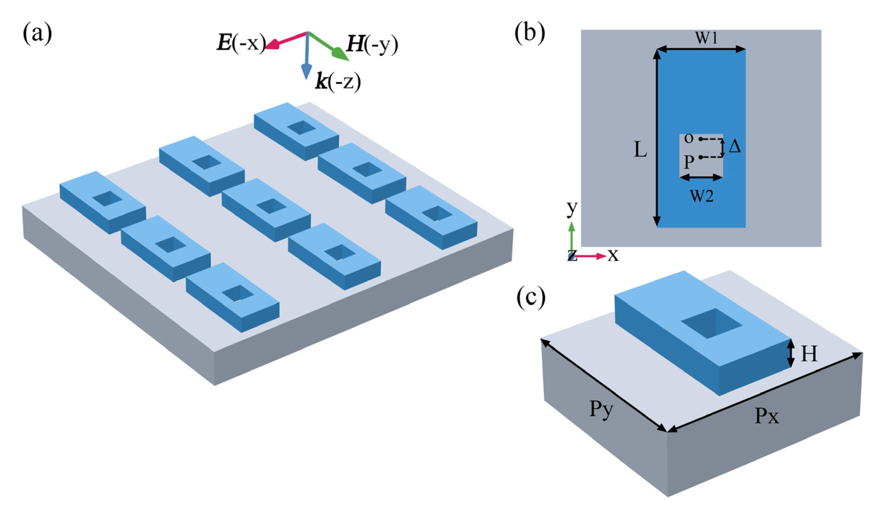
The biosensing platform based on the all-dielectric square nanoholes metasurface is shown in Figure 1. The metasurface structure is formed by a periodic array of silicon (Si) plates with a thickness of 170 nm and nanoholes located on silicon dioxide (SiO2) substrate. Figure 1a shows the schematic diagram of the sensing device of the metasurface. Figure 1b,c represent the unit and top view of the metasurface structure, respectively. The period of the structure is Px = 1100 nm and Py = 990 nm, the side length of the Si plate is W1 = 400 nm and L = 800 nm, and the side length of the square nanohole is W2 = 170 nm, respectively. The center distance between the nanohole and the Si plate along the y-axis is represented by Δ. When Δ is equal to 0, the metasurface structure is completely symmetric, and when Δ is not equal to 0, the in-plane symmetry of the structure is broken. Here we only consider the movement of the nanohole along the negative y axis, and Δ is defined as the asymmetric parameter. We numerically simulated the spectral response of the metasurface using the finite element method, where Floquet periodic boundary conditions are applied in the x, y directions, the incident field is an x-polarized plane wave propagating along the negative z axis, and the refractive index of Si is 3.5, and the refractive index of the SiO2 substrate is set to 1.45.
3. Results and Discussion
3.1. Resonance Performance Analysis
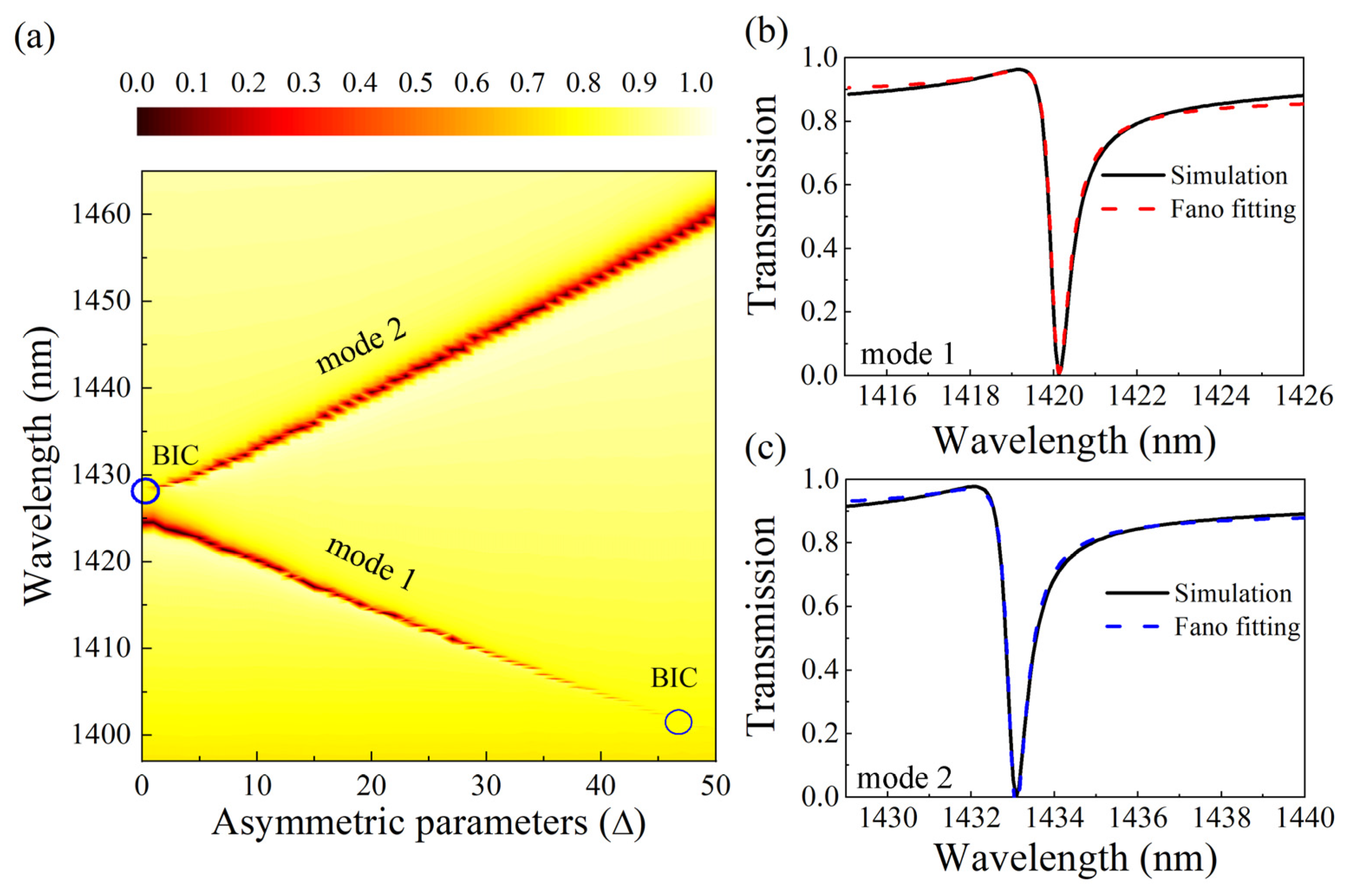
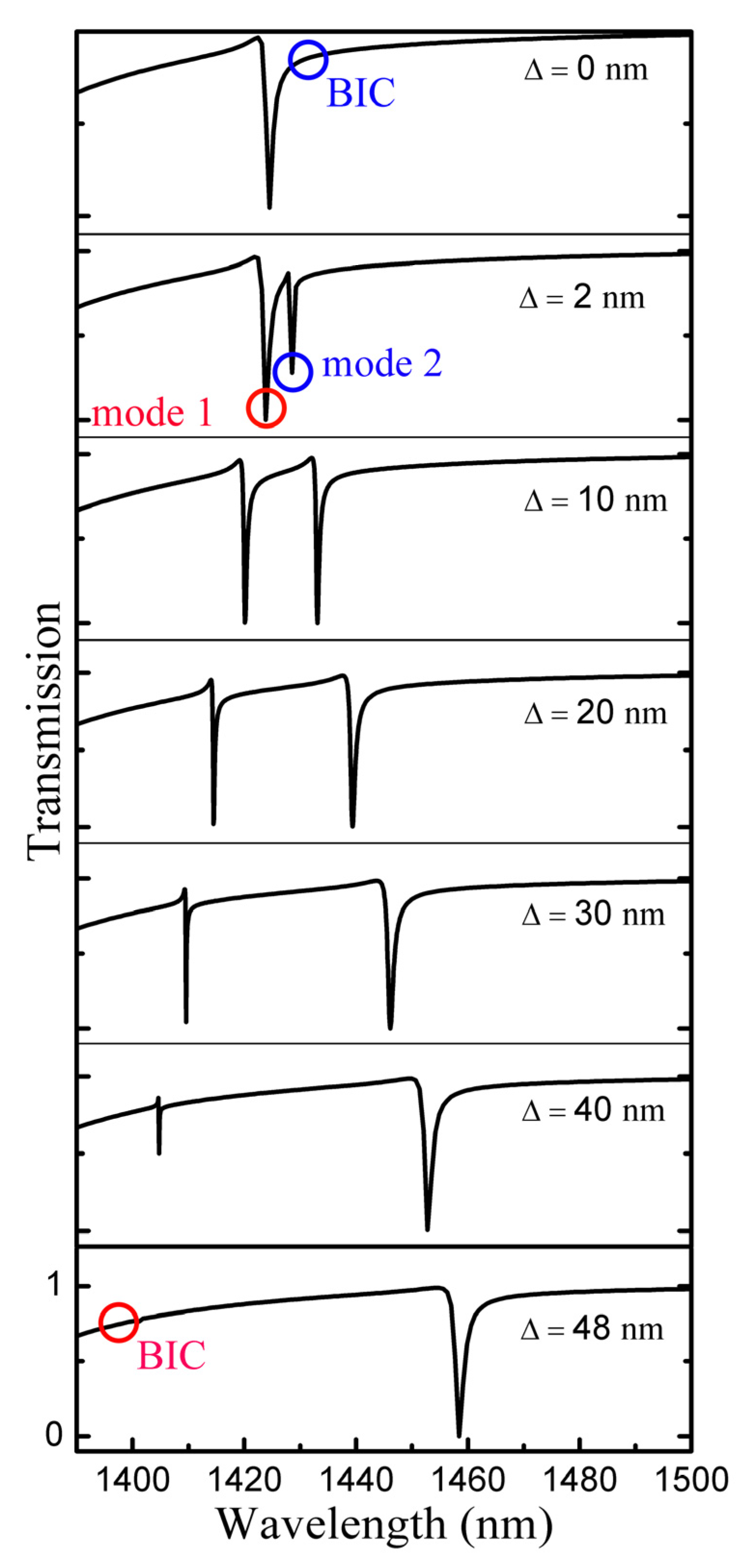
The transmission spectrum for various symmetry parameters Δ is shown in Figure 2a. For mode 1, the resonance peak vanishes at Δ = 0 nm, indicating there is no energy leakage from the bound state to the free space continuum state, and the corresponding radiation Q-factor tends to infinity. However, at Δ ≠ 0 nm, the resonance peak is still visible. A sharp asymmetric linear shape, the Fano resonance, is shown in Figure 2b at Δ = 10 nm. We can observe from Figure 2a, as Δ increases, that the resonance peak of mode 1 becomes wider. This proves that the BIC resonance mode of the excited device is a symmetry-protected BIC mode by breaking the symmetry of the structure. When Δ ≠ 0 nm, the in-plane symmetry of the structural unit is perturbed, and the BIC mode transforms into a quasi-BIC mode that can radiate and have a high Q-factor due to the establishment of a radiative channel between the nonradiative bound state and the free-space continuum state, resulting in more incident light being radiated into the free space. When the translation distance is smaller, the radiation channel is narrower, the radiation loss energy is smaller, and the Q-factor is larger. For mode 2, when Δ = 0 nm, there is resonance peak. Figure 2c depicts the Fano resonance, the sharp asymmetric linear shape, at Δ = 10 nm. The resonance peak of mode 2 gets increasingly narrower as Δ increases. The resonance peak disappears at Δ = 48 nm, corresponding to an accidental BIC that can be explained by destructive interference between resonance modes.
High-Q metasurfaces need more sophisticated manufacturing techniques because their near-field coupling is so susceptible to manufacturing flaws. It is typically more difficult to construct metasurface devices, making it challenging to produce ultra-high-Q metasurface resonators in experiments. The wider the line width of the quasi-BIC mode, the smaller the Q factor.
We can fit the transmission spectra of modes 1 and 2 with the typical Fano formula [40,41]
where ω0 represents the resonance peak frequency, Г represents the resonance attenuation, which is proportional to the resonant peak line width, T0 is background scattering parameter, that is, the electromagnetic wave without any interaction, corresponds to the continuous state, A0 is the coupling coefficient for the continuous state and the discrete state, q is the Breit–Wigner–Fano parameter, which determines the asymmetry of the resonance spectrum.
For asymmetric linear Fano resonances in transmission spectra, we usually determine the radiative Q-factor by fitting the spectra to Equation (1). The Q-factor is calculated using the following formula: . Figure 2b,c show the results of the transmission spectrum curve fitting of the mode 1 and mode 2 at Δ = 10 nm. The resonance wavelength of mode 1 is 1420 nm, and the corresponding Q-factor is 2450, and the resonance wavelength of mode 2 is 1433, and the corresponding Q-factor is 2488.
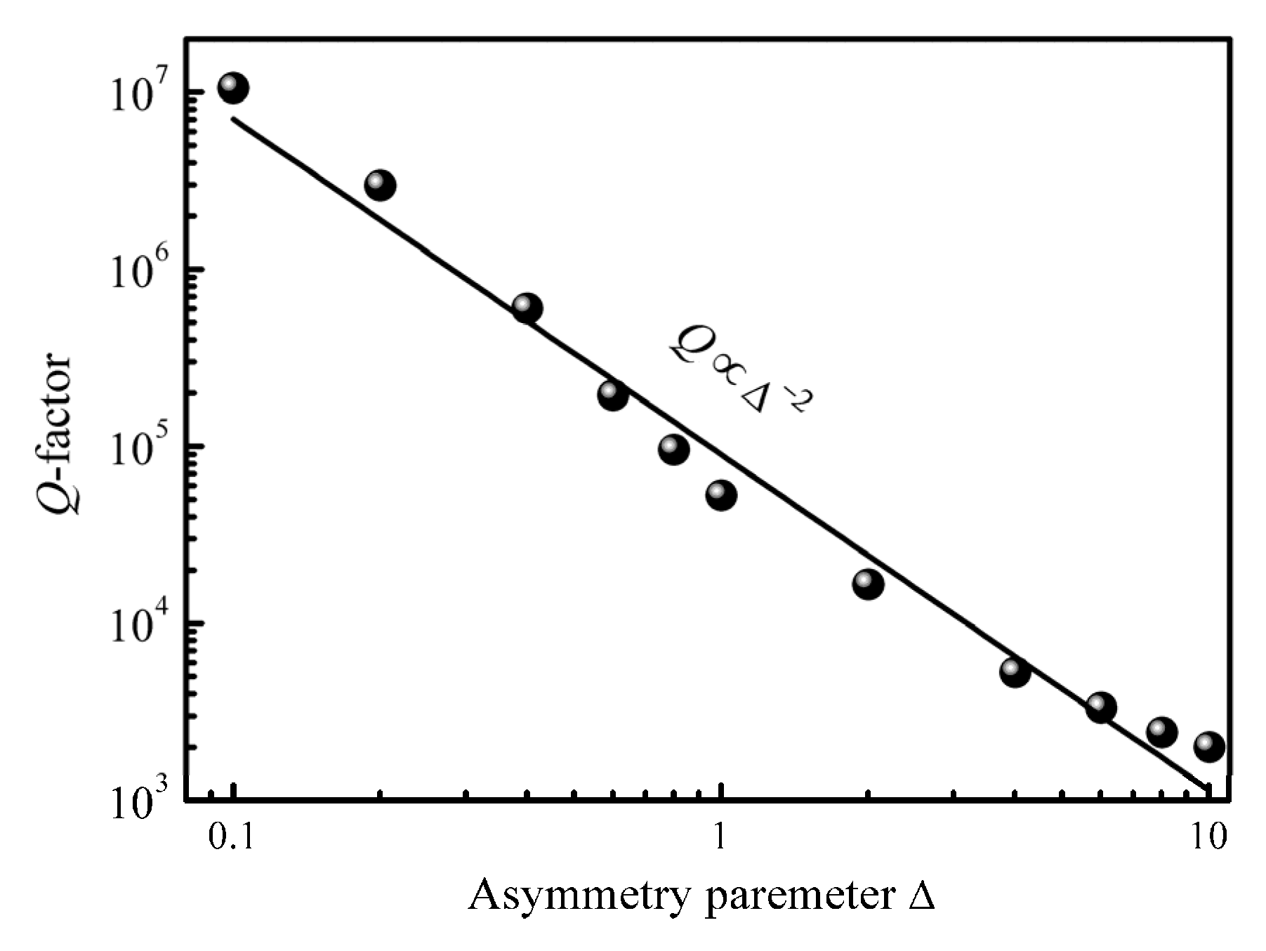
We also investigated the connection between the asymmetry parameter and Q-factor of mode 2, as shown in Figure 3. The continuous state interacts with the bound state and leaks when the structure’s symmetry is disrupted, producing ultra-high Q Fano resonance [26]. Figure 3 shows that Q-factor and the asymmetry parameter meet the quadratic reciprocal relationship Q∝Δ−2, and it can be demonstrated that this mode is a symmetry-protected BIC mode [22,26].
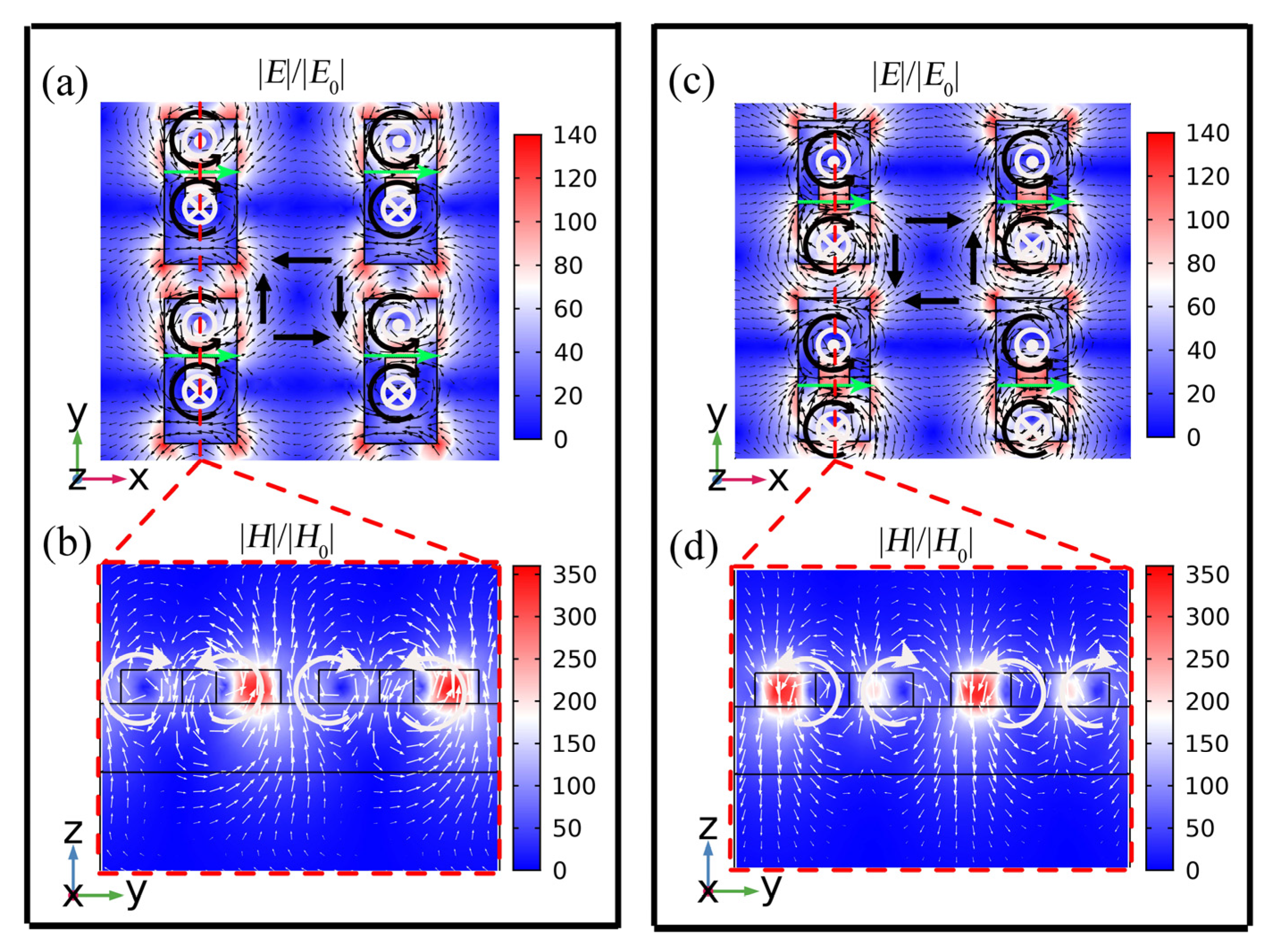
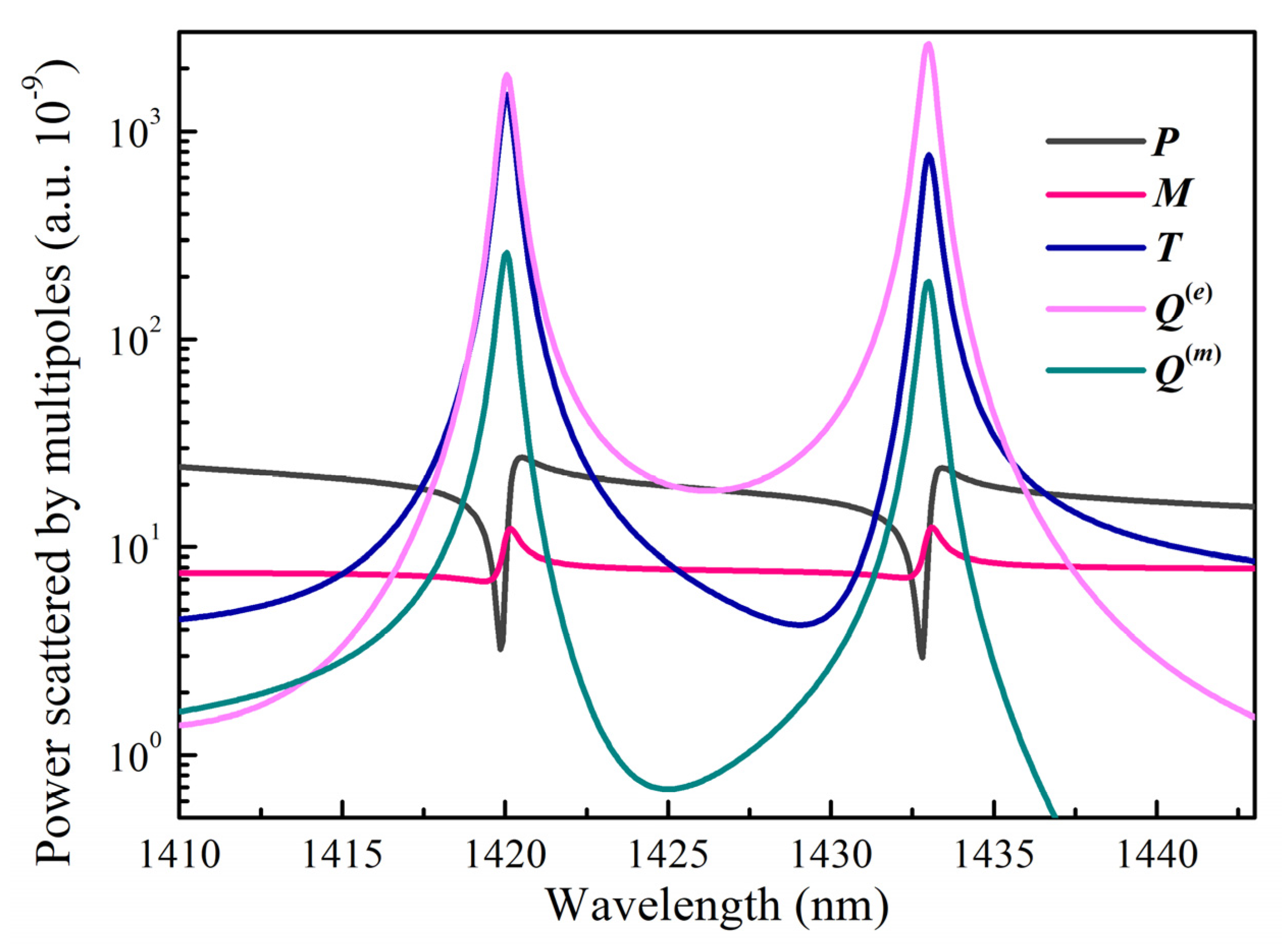
Furthermore, to visualize the electromagnetic excitation modes corresponding to the lowest values of transmittance, we present a schematic diagram of the near-field distribution of the cell structure at the resonant wavelength position, as shown in Figure 4. The field patterns are normalized to the incident electromagnetic field, and the maximum electric field enhancement and magnetic field distribution can be up to 140- and 350-fold, respectively. There are similar field distributions at the resonance wavelength of 1420 nm and 1433 nm. In Figure 4a, the vortex arrows inside the unit structure represent displacement current loops with opposing rotational directions in xoy plane, which excites opposite MDs on the z-axis, and in Figure 4b, the vortex arrows within the structure represent the production of magnetic loops in the yoz plane. Combining the incident light with the x polarization, the circular magnetic ring on the yoz plane excites a strong magnetic TD along the x-axis. At the same time, a pair of reverse rotating currents will also excite the magnetic quadrupole, which has a strong contribution to the resonance response of the metasurface. The displacement current distribution in the structural gap in the xoy plane is an electric quadrupole, as shown in Figure 4a. However, we can only observe the dominant electromagnetic contribution near each resonance in the near-field pattern.
In order to study the characteristics of Fano resonance, we use the multipole decomposition method in the Cartesian coordinate system to calculate the contribution of each multipole to the resonance response. Here, we only consider electric dipoles , magnetic dipoles , and toroidal dipoles . Electrons, electric quadrupoles , and magnetic quadrupoles can be ignored due to the small contribution of higher-order multipoles. The multipole moment is defined as [42,43,44]
where j is the current density vector, r is the position vector, c is the speed of light, ω is the angular frequency, α, β = x, y, z. The scattered power for multipole momentum can be calculated by
The multipole decomposition calculation results in logarithmic coordinates are shown in Figure 5. We can observe that the maximum far-field radiation is mainly contributed by the electric quadrupole and the toroidal dipole at the resonance wavelength of 1420 nm. At the resonance wavelength of 1433 nm, the electric quadrupole dominates the resonance, and the toroidal dipole contributes secondarily. Additionally, the resonance response of the metasurface is significantly influenced by the magnetic quadrupole. The result of the multipole decomposition is consistent with the near-field distribution in the Figure 4.
3.2. Influence of Structural Parameters on Transmission Performance
The calculated transmittance spectra are shown in Figure 6 when Δ changes from 0 nm to 48 nm. As marked by the circles in Figure 6, the radiation Q-factor of mode 2 tends to infinity at Δ = 0 nm, which proves the existence of symmetry-protected BICs. Continuing increasing Δ, the in-plane symmetry of the unit cell is perturbed, allowing the BIC modes to transform to quasi-BIC modes that are radiable and have high Q value and mode 1 appear and become wider. For mode 1, the parameter-tuned BIC is realized by adjusting Δ until the Friedrich–Wintgen condition is met.
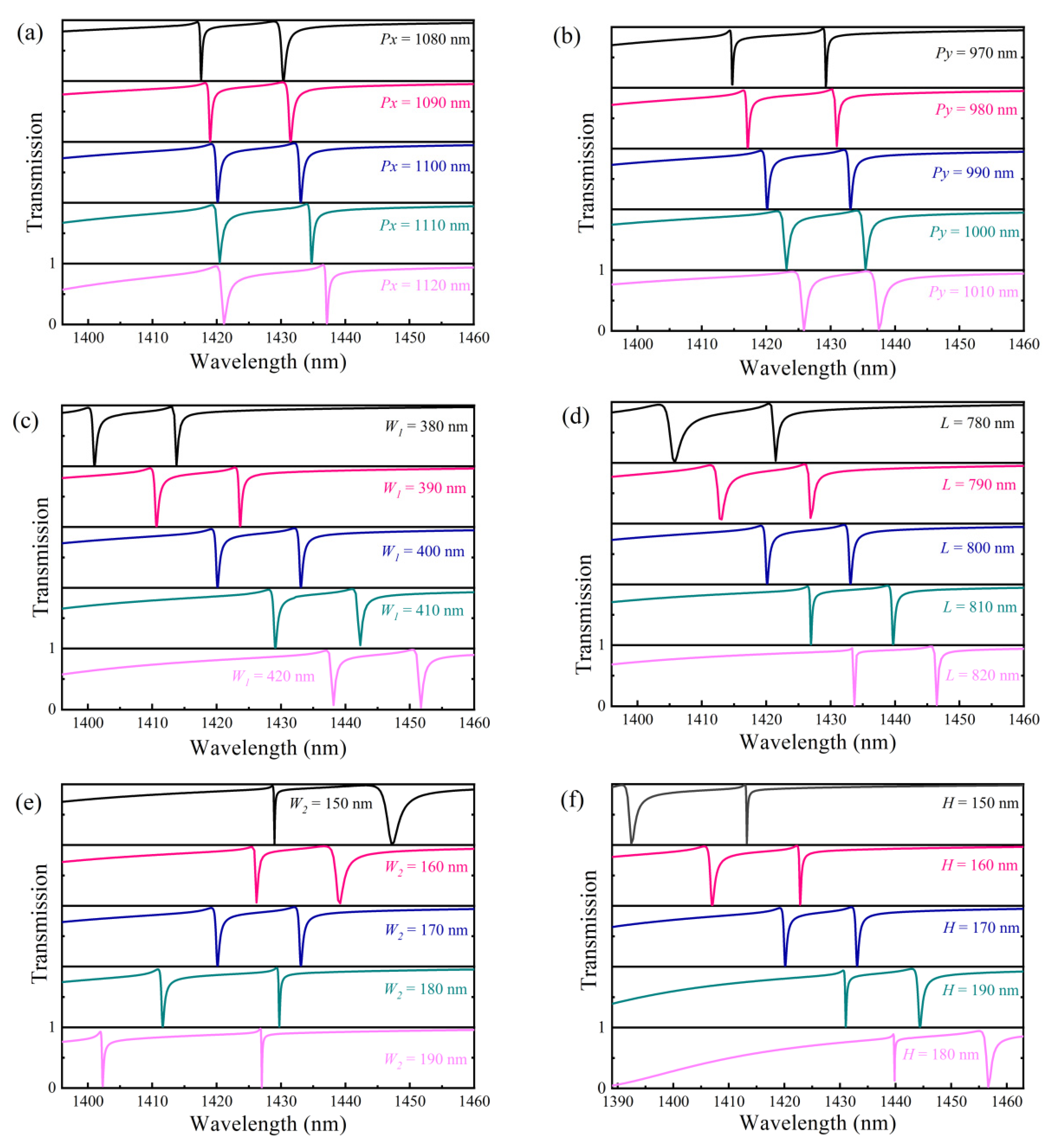
We analyzed the effect of structural parameter changes on the transmission spectrum when Δ = 10 nm, as shown in Figure 7. It is clear that the resonance wavelength is more sensitive to the height and side length of the Si plate and the square nanohole than it is to the period. With the period P increasing, there is a little redshift in the resonance transmission spectrum of the metasurface. As the Si plate’s height H and side lengths W1 and L grow, the resonance becomes noticeably red-shifted. However, the resonance exhibits a distinct blue shift as the square nanohole’s side length rises. It can be explained by the effective refractive index of the metasurface. As the side length of the nanohole increases, the effective refractive index of the metasurface declines, and the interaction between light and matter in the resonant cavity gradually reduces, resulting in a blue shift of the resonance position. As the period, side length of the Si plate increase, the surface area of the metasurface, resulting in an increase in the effective refractive index, and the interaction between light and matter in the resonant cavity gradually increases, resulting in a red shift of the resonance position [45].
The resonant line width and Q-factor, however, are little affected by an increase in period H and side length W1. Additionally, with an increase in side length L from 780 nm to 820 nm, the Q-factor of mode 1 goes from 814 to 14,447 whereas the Q-factor of mode 2 goes from 2268 to 4026. As side length W2 increases from 150 nm to 190 nm, the Q-factor of mode 1 first decreases from 10,347 to 2420, then increases to 5733, whereas the Q-factor of mode 2 increases from 708 to 12,539. While the Q-factor of mode 2 reduces from 7918 to 1552 with an increase in height H from 150 nm to 190, the Q-factor of mode 1 increases from 1239 to 13,091.
3.3. Analysis of Refractive Index Sensing Characteristics
The higher the sensitivity of the sensor, the easier it is to detect small changes in the dielectric properties around the sensor. The sensitivity can be expressed as [46] , where is the variation of the resonance wavelength, is the variation of the refractive index caused by the change of the surrounding environment, and the unit is RIU (Refractive Index Unit). The entire performance of the sensor can be described by its FOM, and a higher FOM value denotes a better performance of the sensor. The FOM can be represented as [47] , where the FWHM is the width at half-peak of the Fano resonance line. A high Q-factor (i.e., narrow line width) indicates that the sensor has strong light-field confinement capabilities, whereas a high sensitivity sensor indicates that more light field leaks from the device into the space. As a result, sensitivity and Q factor have a mutually exclusive relationship that influences the FOM.
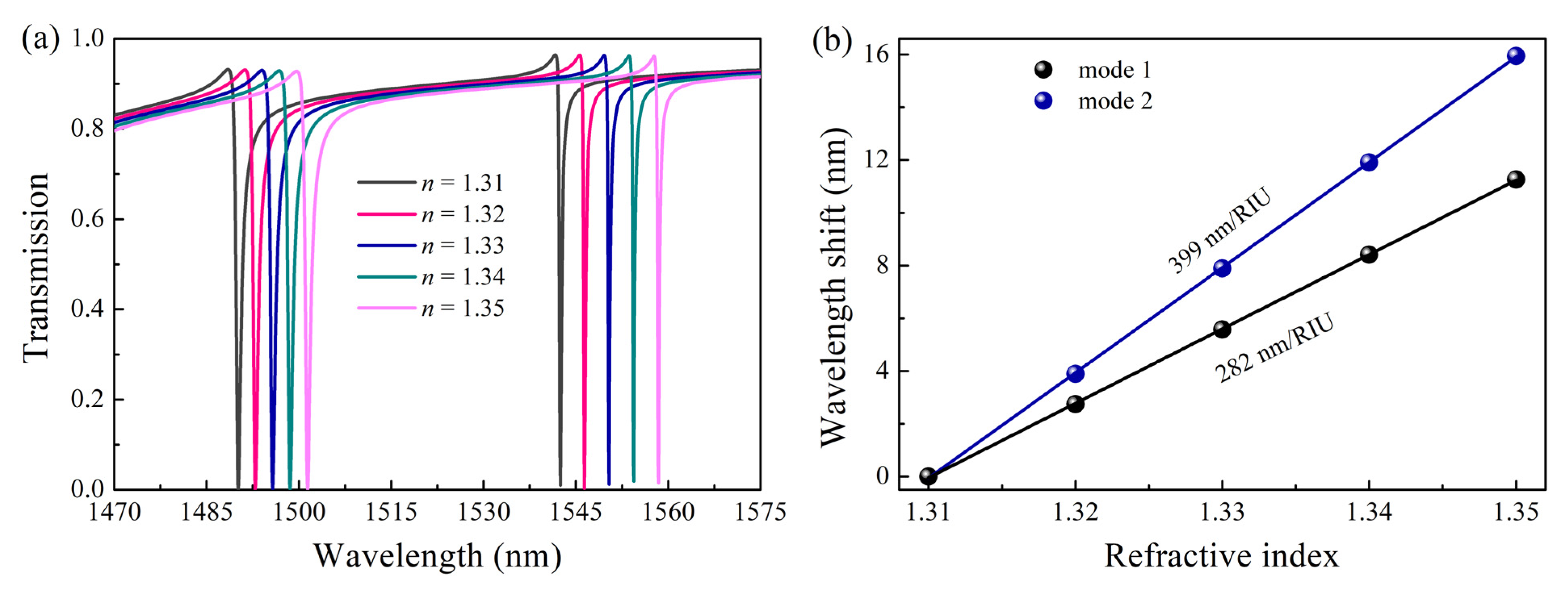
Figure 8a,b illustrate the impact of external media with various refractive indices n on the transmission spectrum. The liquid to be tested with n from 1.31 to 1.35 fills the gap and around the structure, and the thickness of the liquid is 300 nm, and the asymmetric parameter Δ is 30 nm. The increasing of refractive index has little effect on the Q-factor and the peak value of the resonance peaks, and the resonance position exhibits a noticeable redshift. The corresponding sensitivities of each resonance are 282 nm/RIU and 399 nm/RIU, respectively. The related Q factors are 1688 and 4959, while the corresponding FOMs are 308 and 1281, respectively. The field distribution is primarily responsible for the variation in sensing performance between the two resonance modes. Reducing structural asymmetry can further boost the device’s sensitivity and Q factor, which will further enhance FOM. Compared to metal or hybrid metal-dielectric sensors, the FOM are higher. There are certain advantages in sensing performance when compared to some previously proposed architectures [13,14,41]. As shown in Table 1, after comparing our results with previous works, it can be seen that the proposed structure has better sensing performance and simpler structure, providing a valuable reference for future sensor applications.
4. Conclusions
In this paper, an all-dielectric metasurface refractive index sensing platform based on TD and EQ resonance driven by quasi-BIC is proposed and demonstrated theoretically. The resonance in the transmission spectrum evolves from symmetry-protected BIC into quasi-BIC and from quasi-BIC into FW–BIC by translating the nanohole. The physical basis of TD and EQ resonance can be shown by the near-field distribution and multipole decomposition. By analyzing the effect of metasurface on the sensing performance, it was discovered that the maximum sensitivity of the sensor can reach 399 nm/RIU, the quality factor is 4959, and the FOM is 1281. Higher Q values can be obtained with symmetry-protected BIC, and FOM can be further enhanced by lowering the asymmetry parameter. Additionally, by adjusting various structural characteristics, the Fano resonance can be modified to be more advantageous for sensing applications. The proposed metasurface structure is less complicated and more useful than existing complex nanostructures, offering a theoretical benchmark for biochemical sensing platforms.
Author Contributions
Conceptualization and methodology, Z.J. and W.J.; validation, data curation, software and writing—original draft, Z.J.; review and editing, supervision, project administration, funding acquisition, W.J., G.L. and Q.W. All authors have read and agreed to the published version of the manuscript.
Funding
This research was funded by Fujian Province Young and Middle-aged Teacher Education Research Project (No. JAT210562); Embedded Artificial Intelligence Computing and Application Scientific Research Innovation Team of Xiamen Institute of Technology (No. KYTD202003); Xiamen Natural Science Foundation Project (No. United 27).
Data Availability Statement
The data that support the findings of this study are available from the corresponding author upon reasonable request.
Acknowledgments
The authors acknowledge the financial support from Fujian Province Young and Middle-aged Teacher Education Re-search Project (No. JAT210562), Embedded Artificial Intelligence Computing and Application Scientific Research Innovation Team of Xiamen Institute of Technology (No. KYTD202003), and Xiamen Natural Science Foundation Project (No. United 27) for the use of experimental equipment.
Conflicts of Interest
The authors declare no conflict of interest.
References
- Shelby, R.A.; Smith, D.R.; Schultz, S. Experimental Verification of a Negative Index of Refraction. Science 2001, 292, 77–79. [Google Scholar] [CrossRef] [PubMed] [Green Version]
- Kinsey, N.; DeVault, C.; Boltasseva, A.; Shalaev, V.M. Near-zero-index materials for photonics. Nat. Rev. Mater. 2019, 4, 742–760. [Google Scholar] [CrossRef]
- Smith, D.R.; Padilla, W.J.; Vier, D.C.; Nemat-Nasser, S.C.; Schultz, S. Composite Medium with Simultaneously Negative Permeability and Permittivity. Phys. Rev. Lett. 2000, 84, 4184–4187. [Google Scholar] [CrossRef] [PubMed] [Green Version]
- Chen, W.T.; Zhu, A.Y.; Sanjeev, V.; Khorasaninejad, M.; Shi, Z.; Lee, E.; Capasso, F. A broadband achromatic metalens for focusing and imaging in the visible. Nat. Nanotechnol. 2018, 13, 220–226. [Google Scholar] [CrossRef] [Green Version]
- Lu, H.; Guo, X.; Zhang, J.; Zhang, X.; Li, S.; Yang, C. Asymmetric metasurface structures for light absorption enhancement in thin film silicon solar cell. J. Opt. 2019, 21, 045901. [Google Scholar] [CrossRef]
- Chen, T.; Li, S.; Sun, H. Metamaterials application in sensing. Sensors 2012, 12, 2742. [Google Scholar] [CrossRef] [Green Version]
- Neira, A.D.; Wurtz, G.A.; Ginzburg, P.; Zayats, A.V. Ultrafast all-optical modulation with hyperbolic metamaterial integrated in Si photonic circuitry. Opt. Express 2014, 22, 10987–10994. [Google Scholar] [CrossRef] [Green Version]
- Liu, N.; Mesch, M.; Weiss, T.; Hentschel, M.; Giessen, H. Infrared Perfect Absorber and Its Application As Plasmonic Sensor. Nano Lett. 2010, 10, 2342–2348. [Google Scholar] [CrossRef]
- Ding, C.; Jiang, L.; Wu, L.; Gao, R.; Xu, D.; Zhang, G.; Yao, J. Dual-band ultrasensitive THz sensing utilizing high quality Fano and quadrupole resonances in metamaterials. Opt. Commun. 2015, 350, 103–107. [Google Scholar] [CrossRef]
- Jahani, S.; Jacob, Z. All-dielectric metamaterials. Nat. Nanotechnol. 2016, 11, 23–36. [Google Scholar] [CrossRef]
- Bi, K.; Wang, Q.; Xu, J.; Chen, L.; Lan, C.; Lei, M. All-dielectric metamaterial fabrication techniques. Adv. Opt. Mater. 2021, 9, 2001474. [Google Scholar] [CrossRef]
- Cen, W.; Lang, T.; Wang, J.; Xiao, M. High-Q Fano Terahertz resonance based on bound states in the continuum in All-dielectric metasurface. Appl. Surf. Sci. 2022, 575, 151723. [Google Scholar] [CrossRef]
- Jeong, J.; Goldflam, M.D.; Campione, S.; Briscoe, J.L.; Vabishchevich, P.P.; Nogan, J.; Sinclair, M.B.; Luk, T.S.; Brener, I. High Quality Factor Toroidal Resonances in Dielectric Metasurfaces. ACS Photonics 2020, 7, 1699–1707. [Google Scholar] [CrossRef]
- Zhang, Y.; Liang, Z.; Meng, D.; Qin, Z.; Fan, Y.; Shi, X.; Smith, D.R.; Hou, E. All-dielectric refractive index sensor based on Fano resonance with high sensitivity in the mid-infrared region. Results Phys. 2021, 24, 104129. [Google Scholar] [CrossRef]
- Song, S.; Yu, S.; Li, H.; Zhao, T. Ultra-high Q-factor toroidal dipole resonance and magnetic dipole quasi-bound state in the continuum in an all-dielectric hollow metasurface. Laser Phys. 2022, 32, 025403. [Google Scholar] [CrossRef]
- Marinica, D.; Borisov, A.; Shabanov, S. Bound states in the continuum in photonics. Phys. Rev. Lett. 2008, 100, 183902. [Google Scholar] [CrossRef]
- Hsu, C.W.; Zhen, B.; Stone, A.D.; Joannopoulos, J.D.; Soljačić, M. Bound states in the continuum. Nat. Rev. Mater. 2016, 1, 16048. [Google Scholar] [CrossRef] [Green Version]
- Liang, Y.; Koshelev, K.; Zhang, F.; Lin, H.; Lin, S.; Wu, J.; Jia, B.; Kivshar, Y. Bound States in the Continuum in Anisotropic Plasmonic Metasurfaces. Nano Lett. 2020, 20, 6351–6356. [Google Scholar] [CrossRef]
- Liang, Y.; Lin, H.; Lin, S.; Wu, J.; Li, W.; Meng, F.; Yang, Y.; Huang, X.; Jia, B.; Kivshar, Y. Hybrid anisotropic plasmonic metasurfaces with multiple resonances of focused light beams. Nano Lett. 2021, 21, 8917–8923. [Google Scholar] [CrossRef]
- Wang, Y.; Zhou, C.; Huo, Y.; Cui, P.; Song, M.; Liu, T.; Zhao, C.; Liao, Z.; Zhang, Z.; Xie, Y. Efficient Excitation and Tuning of Multi-Fano Resonances with High Q-Factor in All-Dielectric Metasurfaces. Nanomaterials 2022, 12, 2292. [Google Scholar] [CrossRef]
- Zhou, C.; Huang, L.; Jin, R.; Xu, L.; Li, G.; Rahmani, M.; Chen, X.; Lu, W.; Miroshnichenko, A.E. Bound States in the Continuum in Asymmetric Dielectric Metasurfaces. Laser Photonics Rev. 2022, 2200564. [Google Scholar] [CrossRef]
- Koshelev, K.; Lepeshov, S.; Liu, M.; Bogdanov, A.; Kivshar, Y. Asymmetric metasurfaces with high-Q resonances governed by bound states in the continuum. Phys. Rev. Lett. 2018, 121, 193903. [Google Scholar] [CrossRef] [PubMed] [Green Version]
- Bogdanov, A.A.; Koshelev, K.L.; Kapitanova, P.V.; Rybin, M.V.; Gladyshev, S.A.; Sadrieva, Z.F.; Samusev, K.B.; Kivshar, Y.S.; Limonov, M.F. Bound states in the continuum and Fano resonances in the strong mode coupling regime. Adv. Photonics 2019, 1, 016001. [Google Scholar] [CrossRef] [Green Version]
- Han, S.; Cong, L.; Srivastava, Y.K.; Qiang, B.; Rybin, M.V.; Kumar, A.; Jain, R.; Lim, W.X.; Achanta, V.G.; Prabhu, S.S. All-Dielectric Active Terahertz Photonics Driven by Bound States in the Continuum. Adv. Mater. 2019, 31, 1901921. [Google Scholar] [CrossRef]
- Kyaw, C.; Yahiaoui, R.; Burrow, J.A.; Tran, V.; Keelen, K.; Sims, W.; Red, E.C.; Rockward, W.S.; Thomas, M.A.; Sarangan, A. Polarization-selective modulation of supercavity resonances originating from bound states in the continuum. Commun. Phys. 2020, 3, 212. [Google Scholar] [CrossRef]
- Li, S.; Zhou, C.; Liu, T.; Xiao, S. Symmetry-protected bound states in the continuum supported by all-dielectric metasurfaces. Phys. Rev. A 2019, 100, 063803. [Google Scholar] [CrossRef]
- Cong, L.; Singh, R. Symmetry-protected dual bound states in the continuum in metamaterials. Adv. Opt. Mater. 2019, 7, 1900383. [Google Scholar] [CrossRef]
- Fang, C.; Yang, Q.; Yuan, Q.; Gan, X.; Zhao, J.; Shao, Y.; Liu, Y.; Han, G.; Hao, Y. High-Q resonances governed by the quasi-bound states in the continuum in all-dielectric metasurfaces. Opto-Electron. Adv. 2021, 4, 06200030. [Google Scholar] [CrossRef]
- Hu, P.; Wang, J.; Jiang, Q.; Wang, J.; Shi, L.; Han, D.; Zhang, Z.-Q.; Chan, C.T.; Zi, J. Global phase diagram of bound states in the continuum. Optica 2022, 9, 1353–1361. [Google Scholar] [CrossRef]
- Wang, W.; Zheng, L.; Xiong, L.; Qi, J.; Li, B. High Q-factor multiple Fano resonances for high-sensitivity sensing in all-dielectric metamaterials. OSA Contin. 2019, 2, 2818–2825. [Google Scholar] [CrossRef]
- Long, X.; Zhang, M.; Xie, Z.; Tang, M.; Li, L. Sharp Fano resonance induced by all-dielectric asymmetric metasurface. Opt. Commun. 2020, 459, 124942. [Google Scholar] [CrossRef]
- Peng, C.; Feng, C.; Xia, J.; Yap, C.; Zhou, G. Near-infrared Fano resonance in asymmetric silicon metagratings. J. Opt. 2020, 22, 095102. [Google Scholar] [CrossRef]
- Kupriianov, A.S.; Xu, Y.; Sayanskiy, A.; Dmitriev, V.; Kivshar, Y.S.; Tuz, V.R. Metasurface Engineering through Bound States in the Continuum. Phys. Rev. Appl. 2019, 12, 014024. [Google Scholar] [CrossRef] [Green Version]
- Wang, Y.; Han, Z.; Du, Y.; Qin, J. Ultrasensitive terahertz sensing with high-Q toroidal dipole resonance governed by bound states in the continuum in all-dielectric metasurface. Nanophotonics 2021, 10, 1295–1307. [Google Scholar] [CrossRef]
- Campione, S.; Liu, S.; Basilio, L.I.; Warne, L.K.; Langston, W.L.; Luk, T.S.; Wendt, J.R.; Reno, J.L.; Keeler, G.A.; Brener, I. Broken symmetry dielectric resonators for high quality-factor Fano metasurfaces. Acs Photonics 2016, 3, 2362–2367. [Google Scholar] [CrossRef] [Green Version]
- Cui, C.; Zhou, C.; Yuan, S.; Qiu, X.; Zhu, L.; Wang, Y.; Li, Y.; Song, J.; Huang, Q.; Wang, Y. Multiple Fano Resonances in Symmetry-Breaking Silicon Metasurface for Manipulating Light Emission. Acs Photonics 2018, 5, 4074–4080. [Google Scholar] [CrossRef]
- Lopez, G.; Estevez, M.C.; Soler, M.; Lechuga, L. Recent advances in nanoplasmonic biosensors: Applications and lab-on-a-chip integration. Nanophotonics 2016, 6, 123–136. [Google Scholar] [CrossRef]
- Smalley, J.S.T.; Ren, X.; Lee, J.Y.; Ko, W.; Joo, W.-J.; Park, H.; Yang, S.; Wang, Y.; Lee, C.S.; Choo, H.; et al. Subwavelength pixelated CMOS color sensors based on anti-Hermitian metasurface. Nat. Commun. 2020, 11, 3916. [Google Scholar] [CrossRef]
- Zhong, J.; Ghosh, P.; Li, Q. All-Dielectric Metasurface Refractive Index Sensor with Microfluidics. J. Phys. Conf. Ser. 2021, 1838, 012001. [Google Scholar] [CrossRef]
- Lim, W.X.; Manjappa, M.; Pitchappa, P.; Singh, R. Shaping High-Q Planar Fano Resonant Metamaterials toward Futuristic Technologies. Adv. Opt. Mater. 2018, 6, 1800502. [Google Scholar] [CrossRef]
- Yang, L.; Yu, S.; Li, H.; Zhao, T. Multiple Fano resonances excitation on all-dielectric nanohole arrays metasurfaces. Opt. Express 2021, 29, 14907–14916. [Google Scholar] [CrossRef] [PubMed]
- Alaee, R.; Rockstuhl, C.; Fernandez-Corbaton, I. An electromagnetic multipole expansion beyond the long-wavelength approximation. Opt. Commun. 2018, 407, 17–21. [Google Scholar] [CrossRef] [Green Version]
- Song, D.; Wang, H.; Deng, M.; Wang, Y. Toroidal dipole Fano resonances supported by latticeperturbed dielectric nanohole arrays in the nearinfrared region. Appl. Opt. 2021, 60, 3458–3463. [Google Scholar] [CrossRef] [PubMed]
- Zhang, C.; Xue, T.; Zhang, J.; Liu, L.; Xie, J.; Wang, G.; Yao, J.; Zhu, W.; Ye, X. Terahertz toroidal metasurface biosensor for sensitive distinction of lung cancer cells. Nanophotonics 2022, 11, 101–109. [Google Scholar] [CrossRef]
- Zhou, C.; Liu, G.; Ban, G.; Li, S.; Huang, Q.; Xia, J.; Wang, Y.; Zhan, M. Tunable Fano resonator using multilayer graphene in the near-infrared region. Appl. Phys. Lett. 2018, 112, 101904. [Google Scholar] [CrossRef]
- Zhong, Y.; Du, L.; Liu, Q.; Zhu, L.G.; Zhang, B. All-Silicon Terahertz Metasurface With Sharp Fano Resonance and Its Sensing Applications. IEEE Photonics J. 2021, 13, 4600210. [Google Scholar] [CrossRef]
- Maksimov, D.N.; Gerasimov, V.S.; Romano, S.; Polyutov, S.P. Refractive index sensing with optical bound states in the continuum. Opt. Express 2020, 28, 38907–38916. [Google Scholar] [CrossRef]
- Wang, Y.; Sun, C.; Li, H.; Gong, Q.; Chen, J. Self-reference plasmonic sensors based on double Fano resonances. Nanoscale 2017, 9, 11085–11092. [Google Scholar] [CrossRef]
- Zhang, X.; Zhu, X.-S.; Shi, Y.-W. An Optical Fiber Refractive Index Sensor Based on the Hybrid Mode of Tamm and Surface Plasmon Polaritons. Sensors 2018, 18, 2129. [Google Scholar] [CrossRef] [Green Version]
- Yildirim, D.U.; Ghobadi, A.; Soydan, M.C.; Gokbayrak, M.; Toprak, A.; Butun, B.; Ozbay, E. Colorimetric and Near-Absolute Polarization-Insensitive Refractive-Index Sensing in All-Dielectric Guided-Mode Resonance Based Metasurface. J. Phys. Chem. C 2019, 123, 19125–19134. [Google Scholar] [CrossRef]
- Yao, J.; Ou, J.-Y.; Savinov, V.; Chen, M.K.; Kuo, H.Y.; Zheludev, N.I.; Tsai, D.P. Plasmonic anapole metamaterial for refractive index sensing. PhotoniX 2022, 3, 23. [Google Scholar] [CrossRef]
Figure 1.
Schematic diagram of the structure of an all−dielectric metasurface. (a) Schematic diagram of the overall outline of the asymmetric nanohole metasurface; (b) cell structure diagram of the metasurface; (c) top view of the cell structure.
Figure 1.
Schematic diagram of the structure of an all−dielectric metasurface. (a) Schematic diagram of the overall outline of the asymmetric nanohole metasurface; (b) cell structure diagram of the metasurface; (c) top view of the cell structure.

Figure 2.
Metasurface transmission spectrum analysis. (a) Transmission spectra of metasurfaces under different asymmetric parameters; (b,c) Fano fitting of transmission spectra of mode 1 and mode 2, respectively, at Δ = 10 nm; the solid line represents the simulation result, and the dashed line represents the fitting result of the Fano formula.

Figure 3.
Plot of Q-factor of mode 2 as a function of the asymmetric parameter Δ (log-log scale), where the black points are obtained by the simulation method and the black line is fitted to demonstrate the inverse quadratic dependence of Δ.
Figure 3.
Plot of Q-factor of mode 2 as a function of the asymmetric parameter Δ (log-log scale), where the black points are obtained by the simulation method and the black line is fitted to demonstrate the inverse quadratic dependence of Δ.

Figure 4.
Field distribution at resonant wavelength at Δ = 10 nm (a,c) the normalized electric field distribution of the resonant wavelength of mode 1 and mode 2, respectively, in the xoy plane; (b,d) the normalized magnetic field distribution of the resonant wavelength of mode 1 and mode 2, respectively, in the yoz plane. The black arrows represent the displacement current direction, and the white arrows represent the magnetic field direction, and the green arrows represent the toroidal dipoles direction.

Figure 5.
Far−field scattering contributions of electric dipole , magnetic dipole , toroidal dipole , electric quadrupole , and magnetic quadrupole .
Figure 5.
Far−field scattering contributions of electric dipole , magnetic dipole , toroidal dipole , electric quadrupole , and magnetic quadrupole .

Figure 6.
The calculated transmittance spectra when Δ changes from 0 nm to 48 nm. Two resonance responses are marked by mode 1 and 2, respectively.
Figure 6.
The calculated transmittance spectra when Δ changes from 0 nm to 48 nm. Two resonance responses are marked by mode 1 and 2, respectively.

Figure 7.
The influence of structural parameters on resonance characteristics. The influence of (a) the period Px, (b) Py, (c) W1, (d) L, (e) W2, and (f) the height H on the resonance peak.
Figure 7.
The influence of structural parameters on resonance characteristics. The influence of (a) the period Px, (b) Py, (c) W1, (d) L, (e) W2, and (f) the height H on the resonance peak.

Figure 8.
Analysis of sensing performance. (a) Variation of transmission spectra for different analyte’s refractive indices; (b) Refractive index sensitivity of resonance.
Figure 8.
Analysis of sensing performance. (a) Variation of transmission spectra for different analyte’s refractive indices; (b) Refractive index sensitivity of resonance.


Table 1.
Comparison of sensitivity and FOM for various sensors.
| Reference Year | Material | Structure | Sensitivity (nm/RIU) | FOM (RIU−1) |
|---|---|---|---|---|
| [48] 2017 (Exprement) | Au | grating | 470 | 31 |
| [49] 2018 (Simulation) | TiO2/SiO2/Ag | Fiber | 2610 | 168 |
| [50] 2019 (Simulation) | Si3N4, SiO2 | Grating-waveguide | 110 | 190 |
| [13] 2020 (Exprement) | SiO2 | hollow cuboids | 161 | 80 |
| [14] 2021 (Simulation) | Si | Lucky knot | 986 | 32.7 |
| [51] 2022 (Simulation) | Au | Split ring-dumbbell | 445 | 1.5 |
| This work (Simulation) | Si | Square hole | 399 | 1281 |
Disclaimer/Publisher’s Note: The statements, opinions and data contained in all publications are solely those of the individual author(s) and contributor(s) and not of MDPI and/or the editor(s). MDPI and/or the editor(s) disclaim responsibility for any injury to people or property resulting from any ideas, methods, instructions or products referred to in the content. |
© 2023 by the authors. Licensee MDPI, Basel, Switzerland. This article is an open access article distributed under the terms and conditions of the Creative Commons Attribution (CC BY) license (https://creativecommons.org/licenses/by/4.0/).
Share and Cite
MDPI and ACS Style
Jing, Z.; Jiaxian, W.; Lizhen, G.; Weibin, Q. High-Sensitivity Sensing in All-Dielectric Metasurface Driven by Quasi-Bound States in the Continuum. Nanomaterials 2023, 13, 505. https://doi.org/10.3390/nano13030505
AMA Style
Jing Z, Jiaxian W, Lizhen G, Weibin Q. High-Sensitivity Sensing in All-Dielectric Metasurface Driven by Quasi-Bound States in the Continuum. Nanomaterials. 2023; 13(3):505. https://doi.org/10.3390/nano13030505
Chicago/Turabian StyleJing, Zhao, Wang Jiaxian, Gao Lizhen, and Qiu Weibin. 2023. "High-Sensitivity Sensing in All-Dielectric Metasurface Driven by Quasi-Bound States in the Continuum" Nanomaterials 13, no. 3: 505. https://doi.org/10.3390/nano13030505
Note that from the first issue of 2016, this journal uses article numbers instead of page numbers. See further details here.