
Dislocation Filter Based on LT-GaAs Layers for Monolithic GaAs/Si Integration
 , , , , ,
  , and
, and
Abstract
:
1. Introduction
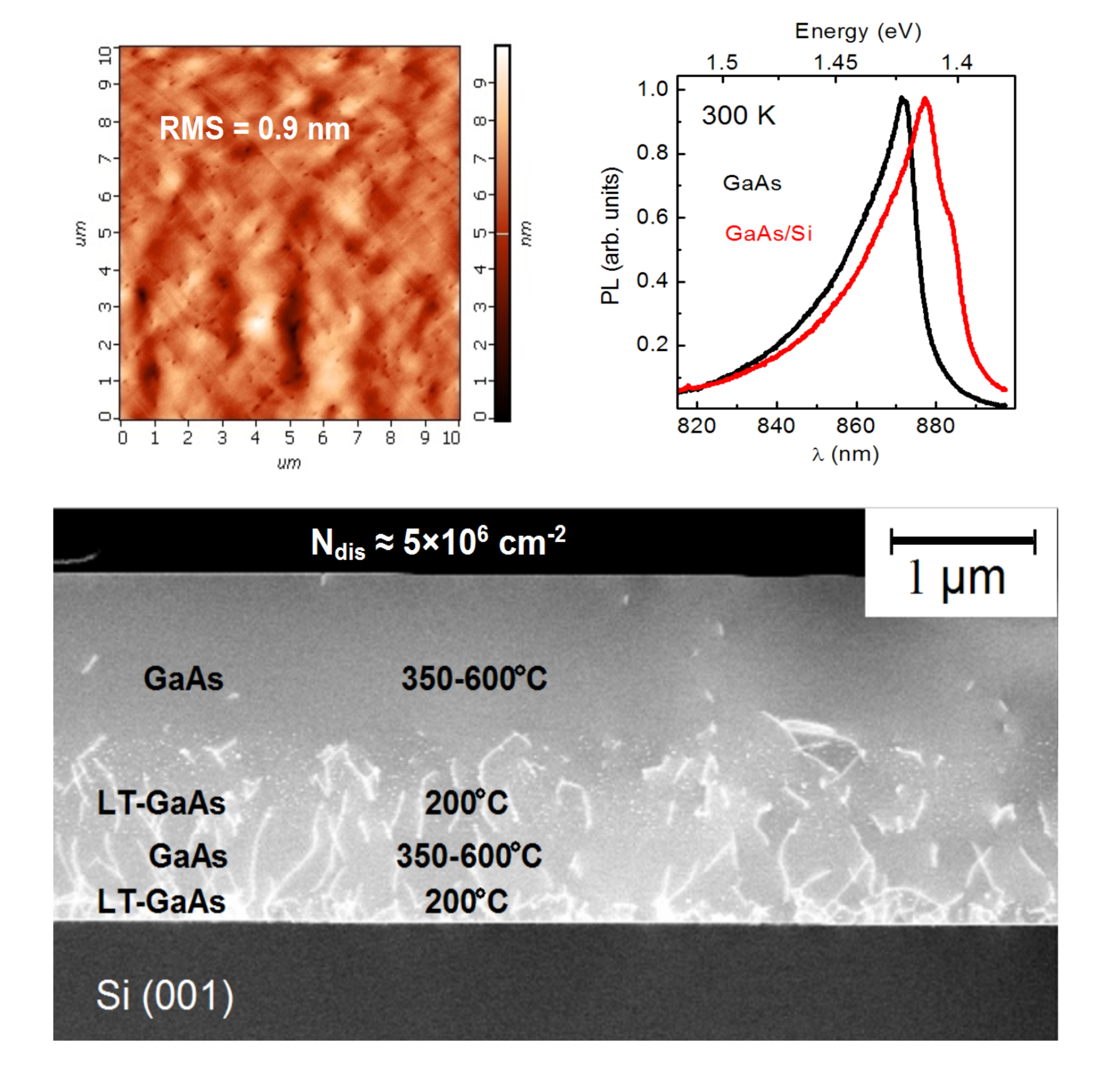
2. Epitaxial GaAs/Si HSs Growth
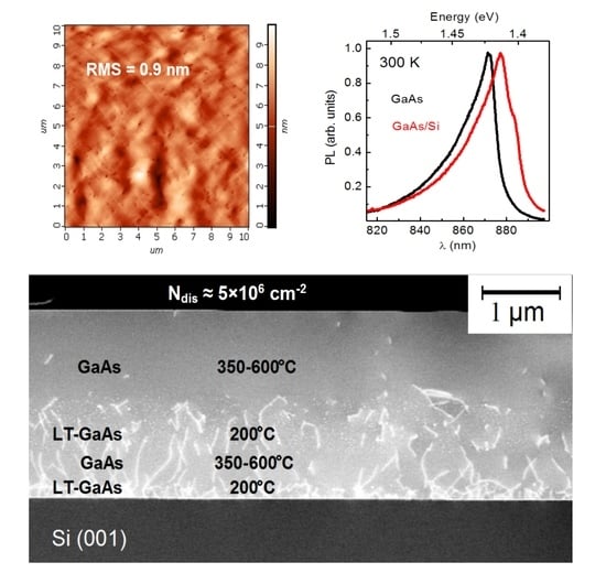
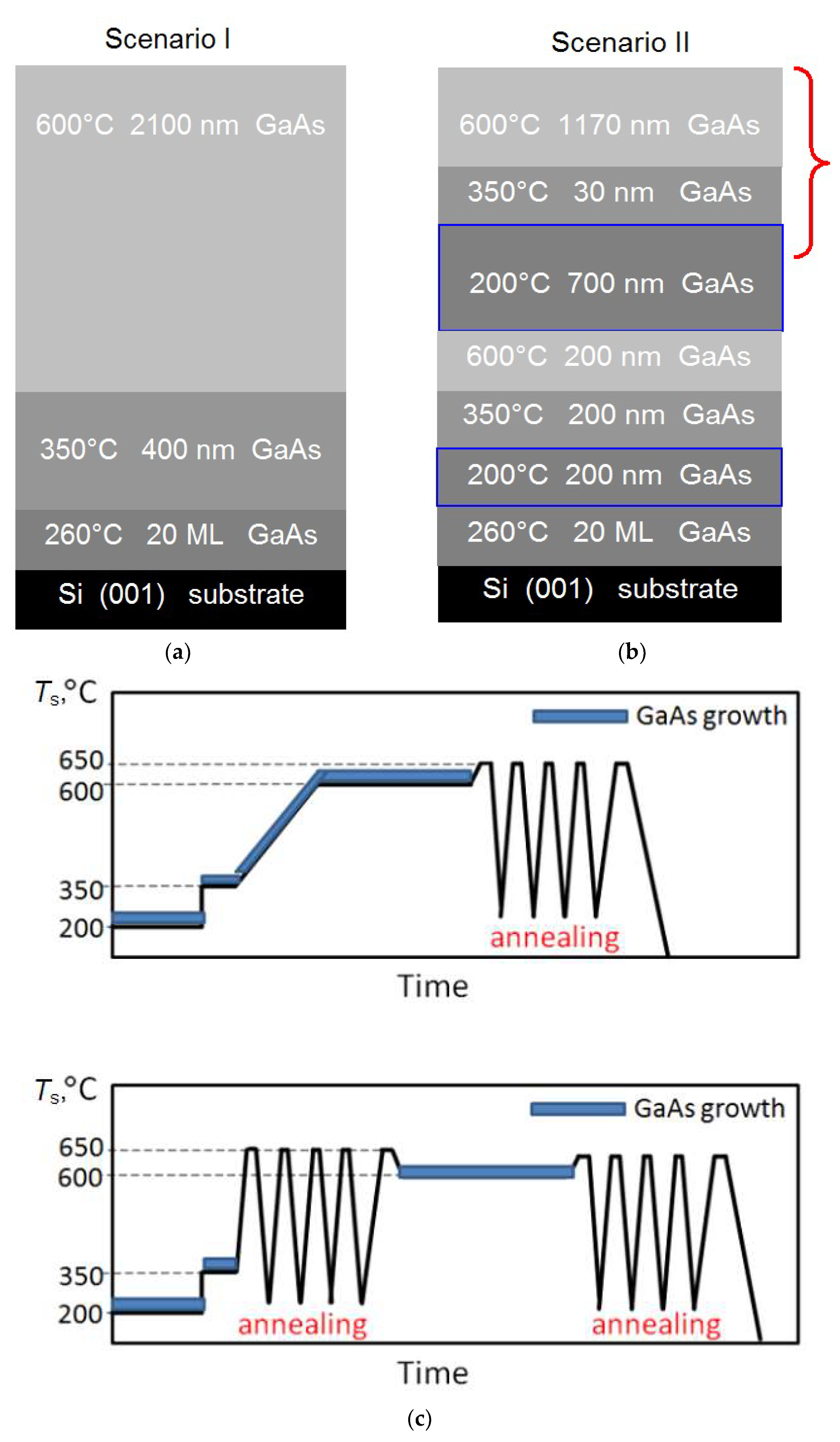
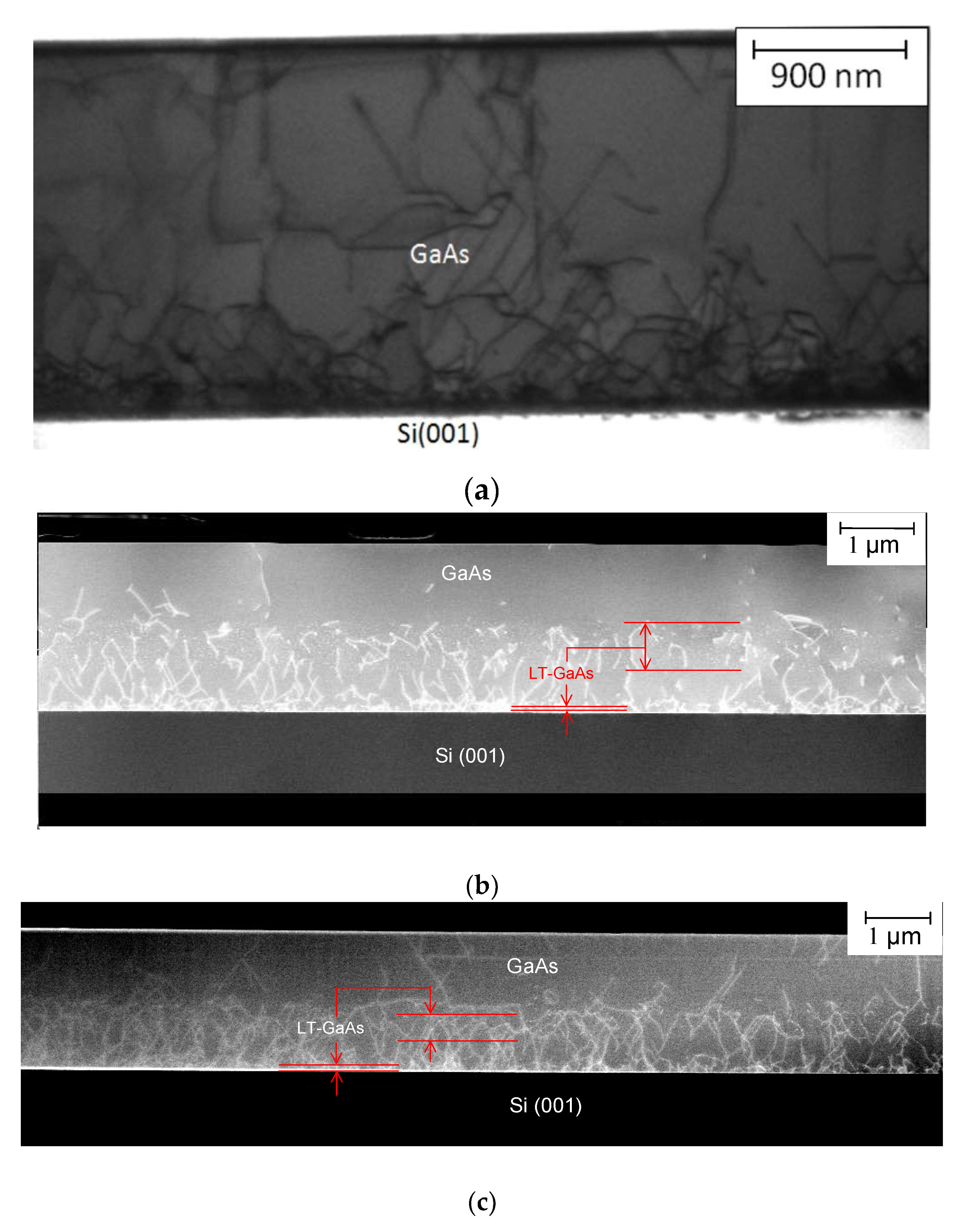
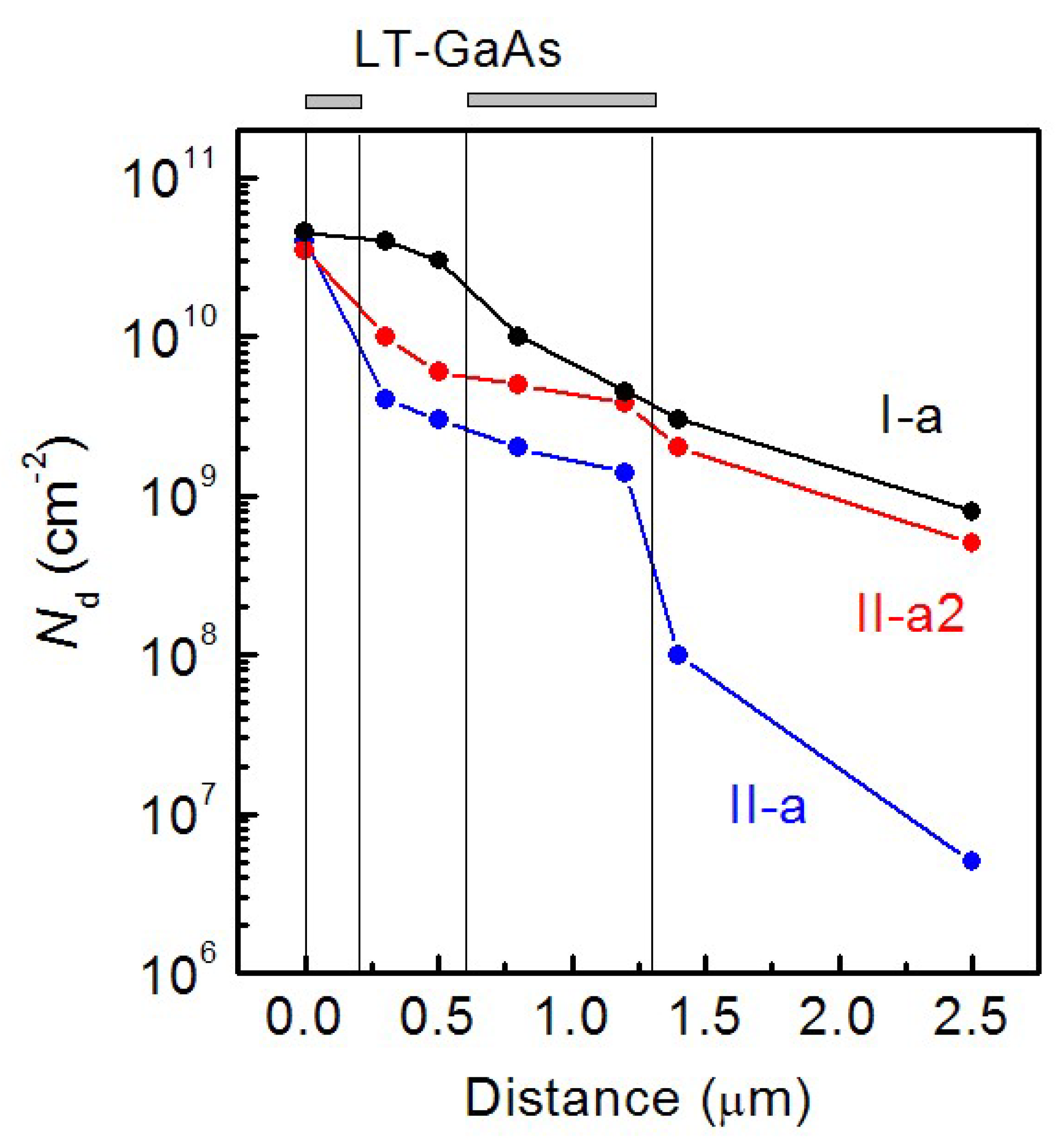
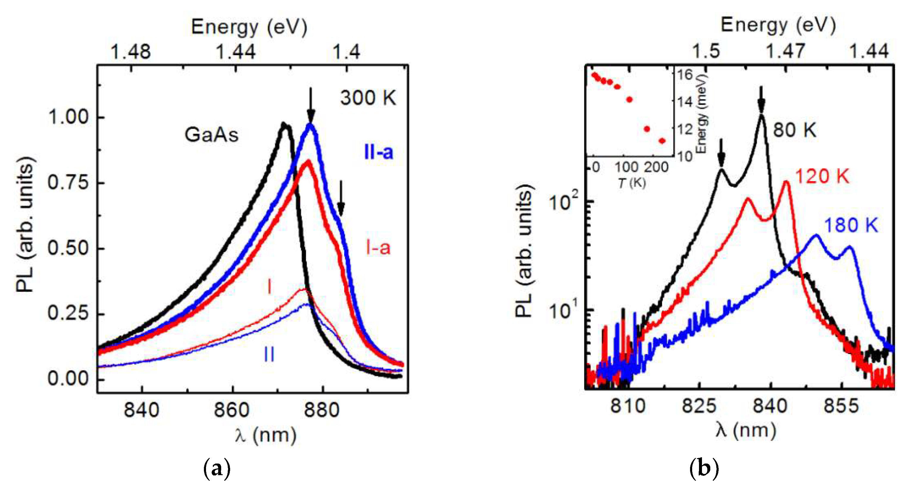
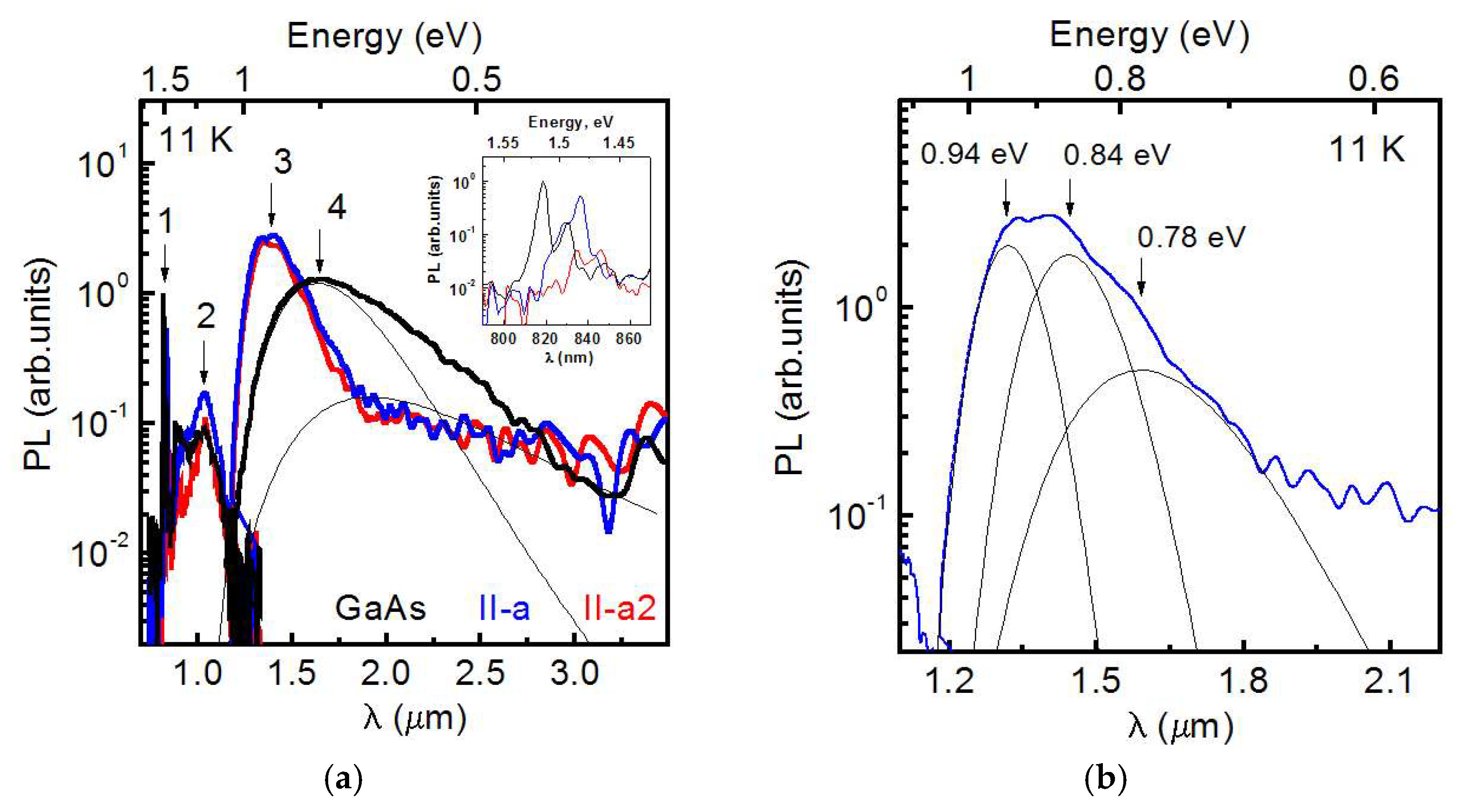
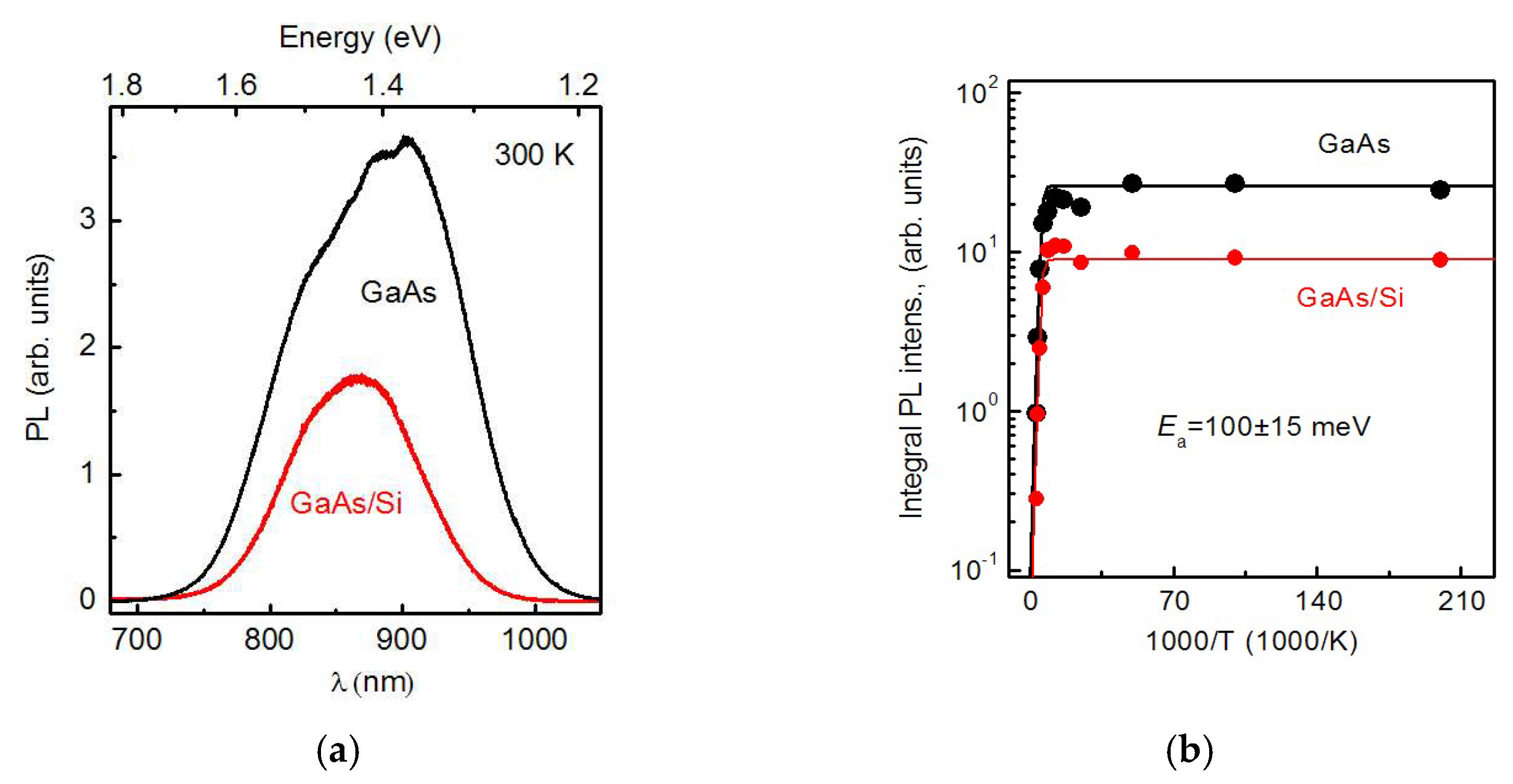
3. Results
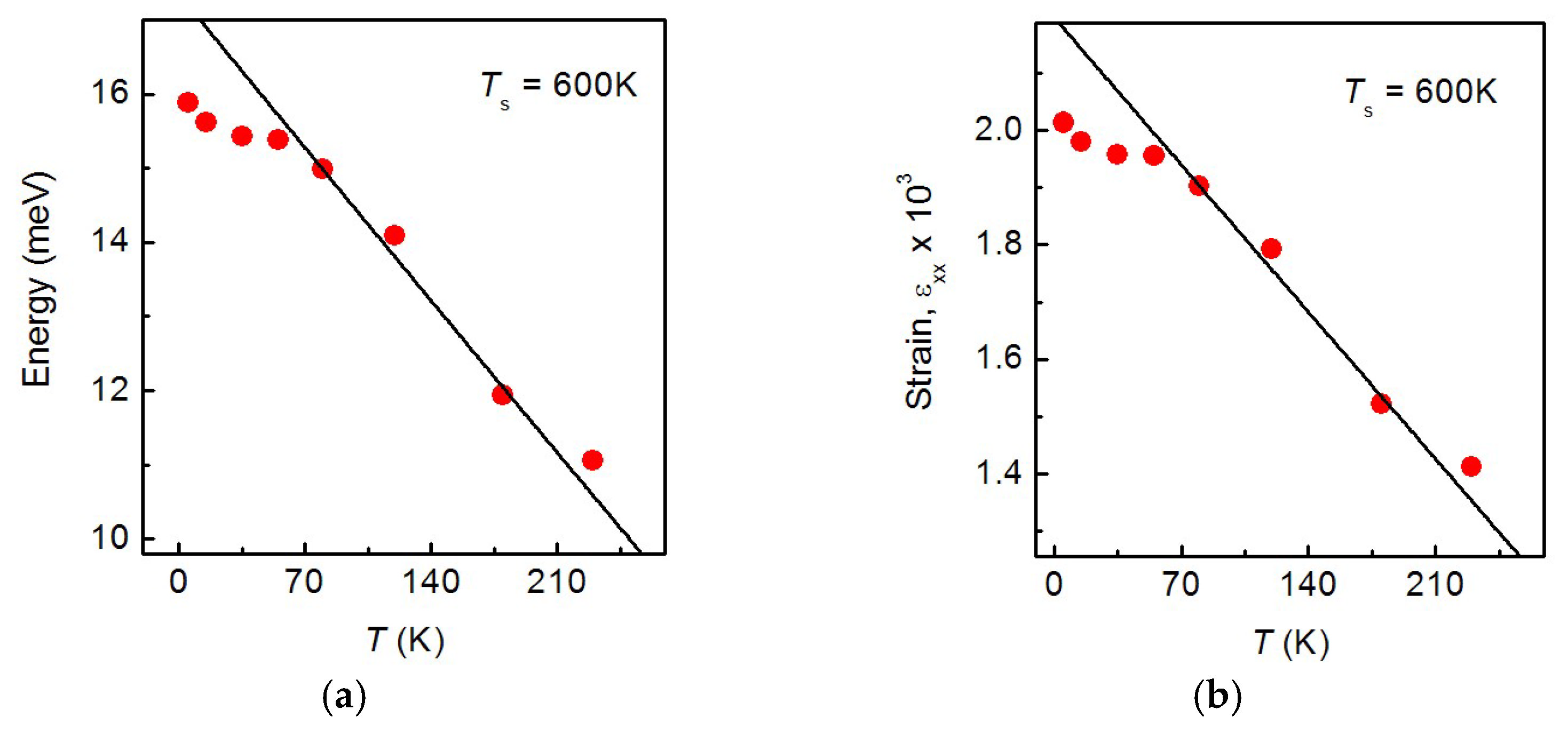
4. Discussion
5. InAs/AlAs SAQDs on the GaAs/Si HS
6. Conclusions
Author Contributions
Funding
Informed Consent Statement
Data Availability Statement
Conflicts of Interest
Appendix A

| Parameter | Value |
|---|---|
| 5.65325 (Å) a | |
| 3.88 × 10⁻⁵ (Å/K) a | |
| 1.81 × 10⁻⁵ (Å/K) b | |
| C11 | 1221 (GPa) a |
| C12 | 566 (GPa) a |
| −7.17 (eV) a | |
| −1.16 (eV) a | |
| −2 (eV) a | |
| 0.341 (eV) a |

References
- Shang, C.; Wan, Y.; Selvidge, J.; Hughes, E.; Herrick, R.; Mukherjee, K.; Duan, J.; Grillot, F.; Chow, W.W.; Bowers, J.E. Perspectives on advances in quantum dot lasers and integration with Si photonic integrated circuits. ACS Photonics 2021, 8, 2555–2566. [Google Scholar] [CrossRef]
- Koval, O.Y.; Fedorov, V.V.; Bolshakov, A.D.; Fedina, S.V.; Kochetkov, F.M.; Neplokh, V.; Mukhin, I.S. Structural and optical properties of self-catalyzed axially heterostructured GaPN/GaP nanowires embedded into a flexible silicone membrane. Nanomaterials 2020, 10, 2110. [Google Scholar] [CrossRef] [PubMed]
- Xu, B.; Wang, G.; Du, Y.; Miao, Y.; Li, B.; Zhao, X.; Lin, H.; Yu, J.; Su, J.; Dong, Y.; et al. Monolithic Integration of O-Band InAs Quantum Dot Lasers with Engineered GaAs Virtual Substrate Based on Silicon. Nanomaterials 2022, 12, 2704. [Google Scholar] [CrossRef] [PubMed]
- Abouzaid, O.; Mehdi, H.; Martin, M.; Moeyaert, J.; Salem, B.; David, S.; Souifi, A.; Chauvin, N.; Hartmann, J.-M.; Ilahi, B.; et al. O-Band Emitting InAs Quantum Dots Grown by MOCVD on a 300 mm Ge-Buffered Si (001) Substrate. Nanomaterials 2020, 10, 2450. [Google Scholar] [CrossRef] [PubMed]
- Dvoretckaia, L.; Gridchin, V.; Mozharov, A.; Maksimova, A.; Dragunova, A.; Melnichenko, I.; Cirlin, G. Light-Emitting Diodes Based on InGaN/GaN Nanowires on Microsphere-Lithography-Patterned Si Substrates. Nanomaterials 2022, 12, 1993. [Google Scholar] [CrossRef]
- Sun, C.; Wade, M.T.; Lee, Y.; Orcutt, J.S.; Alloatti, L.; Georgas, M.S.; Stojanović, V. Single-chip microprocessor that communicates directly using light. Nature 2015, 528, 534–538. [Google Scholar] [CrossRef] [PubMed] [Green Version]
- Yamaguchi, M.; Wang, Y.C.; Kojima, N.; Yamamoto, A.; Ohshita, Y. Low-temperature direct growth for low dislocation density in III-V on Si towards high-efficiency III-V/Si tandem solar cells. Jpn. J. Appl. Phys. 2021, 60, SBBF14. [Google Scholar] [CrossRef]
- Soga, T.; Imori, T.; Umeno, M.; Hattori, S. Stress and strain of GaAs on Si grown by MOCVD using strained superlattice intermediate layers and a two-step growth method. Jpn. J. Appl. Phys. 1987, 26, L536. [Google Scholar] [CrossRef]
- Bolkhovityanov, Yu.B.; Pchelyakov, O.P. GaAs epitaxy on Si substrates: Modern status of research and engineering. PHYS-USP 2008, 51, 437–456. [Google Scholar] [CrossRef]
- Liu, A.Y.; Peters, J.; Huang, X.; Jung, D.; Norman, J.; Lee, M.L.; Gossard, A.C.; Bowers, J.E. Electrically pumped continuous-wave 1.3 μm quantum-dot lasers epitaxially grown on on-axis (001) GaP/Si. Opt. Lett. 2017, 42, 338–341. [Google Scholar] [CrossRef]
- Wei, W.; Feng, Q.; Wang, Z.; Wang, T.; Zhang, J. Perspective: Optically-pumped III–V quantum dot microcavity lasers via CMOS compatible patterned Si (001) substrates. J. Semicond. 2019, 40, 101303. [Google Scholar] [CrossRef]
- Du, Y.; Xu, B.; Wang, G.; Miao, Y.; Li, B.; Kong, Z.; Dong, Y.; Wang, W.; Radamson, H.H. Review of Highly Mismatched III-V Heteroepitaxy Growth on (001) Silicon. Nanomaterials 2022, 12, 741. [Google Scholar] [CrossRef] [PubMed]
- Vurgaftman, I.; Meyer, J.Á.; Ram-Mohan, L.Á. Band parameters for III–V compound semiconductors and their alloys. J. Appl. Phys. 2001, 89, 5815–5875. [Google Scholar] [CrossRef] [Green Version]
- Okada, Y.; Tokumaru, Y. Precise determination of lattice parameter and thermal expansion coefficient of silicon between 300 and 1500 K. J. Appl. Phys. 1984, 56, 314–320. [Google Scholar] [CrossRef]
- Fang, S.F.; Adomi, K.; Iyer, S.; Morkoc, H.; Zabel, H.; Choi, C.; Otsuka, N. Gallium arsenide and other compound semiconductors on silicon. J. Appl. Phys. 1990, 68, R31–R58. [Google Scholar] [CrossRef]
- Bringans, R.D.; Biegelsen, D.K.; Swartz, L.E. Atomic-step rearrangement on Si (100) by interaction with arsenic and the implication for GaAs-on-Si epitaxy. Phys. Rev. B 1991, 44, 3054. [Google Scholar] [CrossRef]
- Pukite, P.R.; Cohen, P.I. Multilayer step formation after As adsorption on Si (100): Nucleation of GaAs on vicinal Si. Appl. Phys. Lett. 1987, 50, 1739–1741. [Google Scholar] [CrossRef]
- Ide, T. Formation of step structures by as deposition on a double-domain si (001) substrate. Phys. Rev. B 1995, 51, 1722. [Google Scholar] [CrossRef]
- Jackson, M.D.; Leibsle, F.M.; Cole, R.J.; Gregory, D.A.C.; Woolf, D.A.; Weightman, P. Scanning tunneling microscope study of defect structures on As-terminated Si (001) surfaces. J. Vac. Sci. Technol. B 1996, 14, 2424. [Google Scholar] [CrossRef]
- Sakamoto, T.; Hashiguchi, G. Si (001)-2×1 single-domain structure obtained by high temperature annealing. Jpn. J. Appl. Phys. 1986, 25, L78. [Google Scholar] [CrossRef]
- Chadi, D.J. Stabilities of single-layer and bilayer steps on Si (001) surfaces. Phys. Rev. Lett. 1987, 59, 1691. [Google Scholar] [CrossRef] [PubMed]
- Georgakilas, A.; Stoemenos, J.; Tsagaraki, K.; Komninou, P.; Flevaris, N.; Panayotatos, P.; Christou, A. Generation and annihilation of antiphase domain boundaries in GaAs on Si grown by molecular beam epitaxy. J. Mater. Res. 1993, 8, 1908–1921. [Google Scholar] [CrossRef]
- Li, Q.; Ng, K.W.; Lau, K.M. Growing antiphase-domain-free GaAs thin films out of highly ordered planar nanowire arrays on exact (001) silicon. Appl. Phys. Lett. 2015, 106, 072105. [Google Scholar] [CrossRef] [Green Version]
- Ueda, O.; Soga, T.; Jimbo, T.; Umeno, M. Direct evidence for self-annihilation of antiphase domains in GaAs/Si heterostructures. Appl. Phys. Lett. 1989, 55, 445–447. [Google Scholar] [CrossRef]
- Yamane, K.; Kobayashi, T.; Furukawa, Y.; Okada, H.; Yonezu, H.; Wakahara, A. Growth of pit-free GaP on Si by suppression of a surface reaction at an initial growth stage. J. Cryst. Growth 2009, 311, 794–797. [Google Scholar] [CrossRef]
- Furukawa, Y.F.Y.; Yonezu, H.Y.H.; Ojima, K.O.K.; Samonji, K.S.K.; Fujimoto, Y.F.Y.; Momose, K.M.K.; Aiki, K.A.K. Control of N content of GaPN grown by molecular beam epitaxy and growth of GaPN lattice matched to Si (100) substrate. Jpn. J. Appl. Phys. 2002, 41, 528. [Google Scholar] [CrossRef]
- Akahori, K.; Wang, G.; Okumura, K.; Soga, T.; Jimbo, T.; Umeno, M. Improvement of the MOCVD-grown InGaP-on-Si towards high-efficiency solar cell application. Sol. Energy Mater. Sol. Cells 2001, 66, 593–598. [Google Scholar] [CrossRef]
- Lee, J.W.; Shichijo, H.; Tsai, H.L.; Matyi, R.J. Defect reduction by thermal annealing of GaAs layers grown by molecular beam epitaxy on Si substrates. Appl. Phys. Lett. 1987, 50, 31–33. [Google Scholar] [CrossRef]
- Yamaguchi, M. Dislocation density reduction in heteroepitaxial III-V compound films on Si substrates for optical devices. J. Mater. Res. 1991, 6, 376–384. [Google Scholar] [CrossRef]
- Akiyama, M.; Kawarada, Y.; Kaminishi, K. Growth of single domain GaAs layer on (100)-oriented Si substrate by MOCVD. Jpn. J. Appl. Phys. 1984, 23, L843. [Google Scholar] [CrossRef]
- Vinokurov, D.A.; Lantratov, V.M.; Sinitsyn, M.A.; Ulin, V.P.; Faleev, N.N. Properties and special features of crystallization of epitaxial GaAs films grown on Si (100) substrates by the method of two-stage deposition using the MOCVD hydride process. Sov. Physics. Semicond. 1991, 25, 617–621. Available online: http://pascal-francis.inist.fr/vibad/index.php?action=getRecordDetail&idt=5158775 (accessed on 20 November 2022).
- Chong, T.C.; Phua, C.C.; Lau, W.S.; Tan, L.S. Effects of low-temperature grown gas intermediate layers on the crystalline quality of GaAs-on-Si epilayers. MRS Online Proc. Libr. 1994, 340, 393–398. [Google Scholar] [CrossRef]
- Yamaguchi, M.; Sugo, M.; Itoh, Y. Misfit stress dependence of dislocation density reduction in GaAs films on Si substrates grown by strained-layer superlattices. Appl. Phys. Lett. 1989, 54, 2568–2570. [Google Scholar] [CrossRef]
- Jung, D.; Callahan, P.G.; Shin, B.; Mukherjee, K.; Gossard, A.C.; Bowers, J.E. Low threading dislocation density GaAs growth on on-axis GaP/Si (001). J. Appl. Phys. 2017, 122, 225703. [Google Scholar] [CrossRef] [Green Version]
- Abramkin, D.S.; Petrushkov, M.O.; Emel’yanov, E.A.; Putyato, M.A.; Semyagin, B.R.; Vasev, A.V.; Shamirzaev, T.S. Influence of a Low-Temperature GaAs Dislocation Filter on the Perfection of GaAs/Si Layers. Optoelectron. Instrum. Data Process. 2018, 54, 181–186. [Google Scholar] [CrossRef]
- Putyato, M.A.; Preobrazhenskii, V.V.; Semyagin, B.R.; Fëklin, D.F.; Pakhanov, N.A.; Emelianov, E.A.; Chikichev, S.I. A valved cracking phosphorus beam source using InP thermal decomposition and its application to MBE growth. Semicond. Sci. Technol. 2009, 24, 055014. [Google Scholar] [CrossRef]
- Preobrazhenskii, V.V.; Putyato, M.A.; Semyagin, B.R. Measurements of parameters of the low-temperature molecular-beam epitaxy of GaAs. Semiconductors 2002, 36, 837–840. [Google Scholar] [CrossRef]
- Preobrazhenskii, V.V.; Putyato, M.A.; Pchelyakov, O.P.; Semyagin, B.R. Surface structure transitions on (0 0 1) GaAs during MBE. J. Cryst. Growth 1999, 201, 166–169. [Google Scholar] [CrossRef]
- Luferau, A.I.; Firsov, D.D.; Komkov, O.S. Infrared photoluminescence spectra measurements using boxcar integrator in the active baseline subtraction mode. J. Phys. Conf. Ser. 2019, 1400, 066035. [Google Scholar] [CrossRef]
- Firsov, D.D.; Komkov, O.S.; Solov’ev, V.A.; Kop’ev, P.S.; Ivanov, S.V. Temperature-dependent photoluminescence of InSb/InAs nanostructures with InSb thickness in the above-monolayer range. J. Phys. D Appl. Phys. 2016, 49, 285108. [Google Scholar] [CrossRef]
- Almuneau, G.; Chouchane, F.; Calvez, S.; Makhloufi, H.; Fontaine, C. Three dimensional confinement technology based on buried patterned AlOx layers: Potentials and applications for VCSEL arrays. In Proceedings of the 15th International Conference on Transparent Optical Networks (ICTON), Cartagena, Spain, 23–27 June 2013; pp. 1–3. [Google Scholar] [CrossRef]
- Lautenschlager, P.; Garriga, M.; Logothetidis, S.; Cardona, M. Interband critical points of GaAs and their temperature dependence. Phys. Rev. B 1987, 35, 9174. [Google Scholar] [CrossRef] [PubMed]
- Zemon, S.; Shastry, S.K.; Norris, P.; Jagannath, C.; Lambert, G. Photoluminescence and photoluminescence excitation spectra of GaAs grown directly on Si. MRS Online Proc. Libr. 1986, 67, 203–208. [Google Scholar] [CrossRef]
- Van de Walle, C.G. Band lineups and deformation potentials in the model-solid theory. Phys. Rev. B 1989, 39, 1871. [Google Scholar] [CrossRef] [PubMed] [Green Version]
- Bogardus, E.H.; Bebb, H.B. Bound-exciton, free-exciton, band-acceptor, donor-acceptor, and auger recombination in GaAs. Phys. Rev. 1968, 176, 993.B.39.1871. [Google Scholar] [CrossRef]
- Shah, J.; Leite, R.C.C.; Gordon, J.P. Donor-acceptor pair recombination involving the first excited state of a donor in GaAs. Phys. Rev. 1968, 176, 938. [Google Scholar] [CrossRef]
- Rossi, J.A.; Wolfe, C.M.; Dimmock, J.O. Acceptor luminescence in high-purity n-type GaAs. Phys. Rev. Lett. 1970, 25, 1614. [Google Scholar] [CrossRef]
- Birey, H.; Sites, J. Radiative transitions induced in gallium arsenide by modest heat treatment. J. Appl. Phys. 1980, 51, 619–624. [Google Scholar] [CrossRef]
- Roca, R.C.; Fukui, K.; Mizuno, H.; Suzuki, M.; Kamiya, I. Below. Bandgap Photoluminescence from GaAs. Phys. Status Solidi (b) 2020, 257, 1900391. [Google Scholar] [CrossRef]
- Shin, K.C.; Kwark, M.H.; Choi, M.H.; Oh, M.H.; Tak, Y.B. Photoluminescence investigation of the 1.356 eV band and stoichiometry in undoped GaAs. J. Appl. Phys. 1989, 65, 736–741. [Google Scholar] [CrossRef]
- Kolesnikova, I.A.; Kobtsev, D.A.; Redkin, R.A.; Voevodin, V.I.; Tyazhev, A.V.; Tolbanov, O.P.; Atuchin, V.V. Optical Pump–Terahertz Probe Study of HR GaAs: Cr and SI GaAs: EL2 Structures with Long Charge Carrier Lifetimes. Photonics 2021, 8, 575. [Google Scholar] [CrossRef]
- Zhongji, Z.; Yuanxi, Z. Identification of two bands in the PL spectra of SI LEC GaAs on the basis of a strain model. Mater. Lett. 1986, 4, 286–289. [Google Scholar] [CrossRef]
- Haegel, N.M.; Winnacker, A.; Leo, K.; Rühle, W.W.; Gisdakis, S. Effects of annealing on lifetime and deep-level photoluminescence in semi-insulating gallium arsenide. J. Appl. Phys. 1987, 62, 2946–2949. [Google Scholar] [CrossRef]
- Haegel, N.M.; Kao, Y.J. Bulk and near-surface annealing behavior of the 0.8 eV luminescence in semi-insulating gallium arsenide. Appl. Phys. 1990, A50, 249–253. [Google Scholar] [CrossRef]
- Liang, J.; Li, P.; Gao, Y.; Zhao, J. The near-infrared photoluminescence of GaAs epilayers grown on Si. J. Mater. Sci. 1997, 32, 4377–4382. [Google Scholar] [CrossRef]
- Kumar, R.; Bag, A.; Mukhopadhyay, P.; Das, S.; Biswas, D. Investigation of cross-hatch surface and study of anisotropic relaxation and dislocation on InGaAs on GaAs (001). Electron. Mater. Lett. 2016, 12, 356–364. [Google Scholar] [CrossRef]
- Xie, S.Y.; Yoon, S.F.; Wang, S.Z. Effects of thermal annealing on deep-level defects and minority-carrier electron diffusion length in Be-doped InGaAsN. J. Appl. Phys. 2005, 97, 073702. [Google Scholar] [CrossRef]
- Kaminska, M.; Weber, E.R.; Liliental-Weber, Z.; Leon, R.; Rek, Z.U. Stoichiometry-related defects in GaAs grown by molecular-beam epitaxy at low temperatures. J. Vac. Sci. Technol. B 1989, 7, 710–713. [Google Scholar] [CrossRef]
- Kaminska, M.; Liliental-Weber, Z.; Weber, E.R.; George, T.; Kortright, J.B.; Smith, F.W.; Calawa, A.R. Structural properties of As-rich GaAs grown by molecular beam epitaxy at low temperatures. Appl. Phys. Lett. 1989, 54, 1881–1883. [Google Scholar] [CrossRef]
- Von Bardeleben, H.J.; Manasreh, M.O.; Look, D.C.; Evans, K.R.; Stutz, C.E. Electron-paramagnetic-resonance study of GaAs grown by low-temperature molecular-beam epitaxy. Phys. Rev. B 1992, 45, 3372. [Google Scholar] [CrossRef] [Green Version]
- Liu, X.; Prasad, A.; Nishio, J.; Weber, E.R.; Liliental-Weber, Z.; Walukiewicz, W. Native point defects in low-temperature-grown GaAs. Appl. Phys. Lett. 1995, 67, 279–281. [Google Scholar] [CrossRef]
- Gebauer, J.; Börner, F.; Krause-Rehberg, R.; Staab, T.E.M.; Bauer-Kugelmann, W.; Kögel, G.; Luysberg, M. Defect identification in GaAs grown at low temperatures by positron annihilation. J. Appl. Phys. 2000, 87, 8368–8379. [Google Scholar] [CrossRef] [Green Version]
- Keeble, D.J.; Umlor, M.T.; Asoka-Kumar, P.; Lynn, K.G.; Cooke, P.W. Annealing of low-temperature GaAs studied using a variable energy positron beam. Appl. Phys. Lett. 1993, 63, 87–89. [Google Scholar] [CrossRef]
- Ohbu, I.; Takahama, M.T.M.; Imamura, Y.I.Y. Diffusion of gallium vacancies from low-temperature-grown GaAs. Jpn. J. Appl. Phys. 1992, 31, L1647. [Google Scholar] [CrossRef]
- Islam, M.T.; Chen, X.; Kujofsa, T.; Ayers, J.E. Threading Dislocations in Metamorphic Semiconductor Buffer Layers Containing Chirped Superlattices. Int. J. High Speed Electron. Syst. 2018, 27, 1840028. [Google Scholar] [CrossRef]
- Sharan, S.; Narayan, J.; Fan, J.C.C. Dislocation density reduction in GaAs epilayers on Si using strained layer superlattices. J. Electron. Mater. 1991, 20, 779–784. [Google Scholar] [CrossRef]
- Yakimov, A.I.; Kirienko, V.V.; Utkin, D.E.; Dvurechenskii, A.V. Light-Trapping-Enhanced Photodetection in Ge/Si Quantum Dot Photodiodes Containing Microhole Arrays with Different Hole Depths. Nanomaterials 2022, 12, 2993. [Google Scholar] [CrossRef]
- Yu, P.; Wu, J.; Gao, L.; Liu, H.; Wang, Z. InGaAs and GaAs quantum dot solar cells grown by droplet epitaxy. Sol. Energy Mater. Sol. Cells 2017, 161, 377–381. [Google Scholar] [CrossRef]
- Von Helversen, M.; Haisler, A.V.; Daurtsev, M.P.; Dmitriev, D.V.; Toropov, A.I.; Rodt, S.; Reitzenstein, S. Triggered Single-Photon Emission of Resonantly Excited Quantum Dots Grown on (111) B GaAs Substrate. Phys. Status Solidi (RRL) 2022, 16, 2200133. [Google Scholar] [CrossRef]
- Abramkin, D.S.; Atuchin, V.V. Novel InGaSb/AlP Quantum Dots for Non-Volatile Memories. Nanomaterials 2022, 12, 3794. [Google Scholar] [CrossRef] [PubMed]
- Marent, A.; Nowozin, T.; Geller, M.; Bimberg, D. The QD-Flash: A quantum dot-based memory device. Semicond. Sci. Technol. 2010, 26, 014026. [Google Scholar] [CrossRef]
- Huang, X.; Su, R.; Yang, J.; Rao, M.; Liu, J.; Yu, Y.; Yu, S. Wafer-scale epitaxial low density InAs/GaAs quantum dot for single photon emitter in three-inch substrate. Nanomaterials 2021, 11, 930. [Google Scholar] [CrossRef] [PubMed]
- Wang, Z.M. (Ed.) Self-Assembled Quantum Dots; Springer Science & Business Media: New York, NY, USA, 2007; Volume 1, ISBN-13 978-0-387-74190-1; e-ISBN-13 978-0-387-74191-8. [Google Scholar]
- Shamirzaev, T.S.; Nenashev, A.V.; Gutakovskii, A.K.; Kalagin, A.K.; Zhuravlev, K.S.; Larsson, M.; Holtz, P.O. Atomic and energy structure of InAs/AlAs quantum dots. Phys. Rev. B 2008, 78, 085323. [Google Scholar] [CrossRef]
- Jung, D.; Norman, J.; Kennedy, M.J.; Shang, C.; Shin, B.; Wan, Y.; Gossard, A.C.; Bowers, J.E. High efficiency low threshold current 1.3 μm InAs quantum dot lasers on on-axis (001) GaP/Si. Appl. Phys. Lett. 2017, 111, 122107. [Google Scholar] [CrossRef]
- Jung, D.; Herrick, R.; Norman, J.; Turnlund, K.; Jan, C.; Feng, K.; Gossard, A.C.; Bowers, J.E. Impact of threading dislocation density on the lifetime of InAs quantum dot lasers on Si. Appl. Phys. Lett. 2018, 112, 153507. [Google Scholar] [CrossRef]
- Inoue, D.; Wan, Y.; Jung, D.; Norman, J.; Shang, C.; Nishiyama, N.; Arai, S.; Gossard, A.C.; Bowers, J.E. Low-dark current 10 Gbit/s operation of InAs/InGaAs quantum dot p-i-n photodiode grown on on-axis (001) GaP/Si. Appl. Phys. Lett. 2018, 113, 093506. [Google Scholar] [CrossRef]
- Xue, Y.; Wang, Y.; Luo, W.; Huang, J.; Lin, L.; Tsang, H.K.; Lau, K.M. Telecom InP-based quantum dash photodetectors grown on Si. Appl. Phys. Lett. 2021, 118, 141101. [Google Scholar] [CrossRef]
- Vim, W.M.; Paff, R.J. Thermal expansion of AIN, sapphire, and silicon. J. Appl. Phys. 1974, 45, 1456. [Google Scholar] [CrossRef]


| HS | I | I-a | II | II-a | II-a2 |
|---|---|---|---|---|---|
| Growth scenario | No LT-GaAs | No LT-GaAs | LT-GaAs | LT-GaAs | LT-GaAs |
| Post-growth annealing | No | Yes | No | Yes | Yes |
| TS increasing scenario after the second LT-GaAs layer | - | - | Gradually, during the growth | Gradually, during the growth | Cyclic annealing |
Publisher’s Note: MDPI stays neutral with regard to jurisdictional claims in published maps and institutional affiliations. |
© 2022 by the authors. Licensee MDPI, Basel, Switzerland. This article is an open access article distributed under the terms and conditions of the Creative Commons Attribution (CC BY) license (https://creativecommons.org/licenses/by/4.0/).
Share and Cite
Petrushkov, M.O.; Abramkin, D.S.; Emelyanov, E.A.; Putyato, M.A.; Komkov, O.S.; Firsov, D.D.; Vasev, A.V.; Yesin, M.Y.; Bakarov, A.K.; Loshkarev, I.D.; et al. Dislocation Filter Based on LT-GaAs Layers for Monolithic GaAs/Si Integration. Nanomaterials 2022, 12, 4449. https://doi.org/10.3390/nano12244449
Petrushkov MO, Abramkin DS, Emelyanov EA, Putyato MA, Komkov OS, Firsov DD, Vasev AV, Yesin MY, Bakarov AK, Loshkarev ID, et al. Dislocation Filter Based on LT-GaAs Layers for Monolithic GaAs/Si Integration. Nanomaterials. 2022; 12(24):4449. https://doi.org/10.3390/nano12244449
Chicago/Turabian StylePetrushkov, Mikhail O., Demid S. Abramkin, Eugeny A. Emelyanov, Mikhail A. Putyato, Oleg S. Komkov, Dmitrii D. Firsov, Andrey V. Vasev, Mikhail Yu. Yesin, Askhat K. Bakarov, Ivan D. Loshkarev, and et al. 2022. "Dislocation Filter Based on LT-GaAs Layers for Monolithic GaAs/Si Integration" Nanomaterials 12, no. 24: 4449. https://doi.org/10.3390/nano12244449