Article

Features of Galvanostatic Electrodeposition of NiFe Films with Composition Gradient: Influence of Substrate Characteristics

by
Tatiana I. Zubar
1,2,*,
Tatsiana I. Usovich
1,*,
Daria I. Tishkevich
1,2,
Oleg D. Kanafyev
1,
Vladimir A. Fedkin
1,
Anna N. Kotelnikova
1,
Maria I. Panasyuk
1,
Alexander S. Kurochka
3,
Alexander V. Nuriev
3,
Abubakr M. Idris
4,5,
Mayeen U. Khandaker
6,7,
Sergei V. Trukhanov
1,3,
Valery M. Fedosyuk
1 and
Alex V. Trukhanov
1,3
1
Laboratory of Magnetic Films Physics, Scientific-Practical Materials Research Centre of National Academy of Sciences of Belarus, 220072 Minsk, Belarus
2
Laboratory of Single Crystal Growth, South Ural State University, 454080 Chelyabinsk, Russia
3
Department of Electronic Materials Technology, National University of Science and Technology MISiS, 119049 Moscow, Russia
4
Department of Chemistry, College of Science, King Khalid University, Abha 62529, Saudi Arabia
5
Research Center for Advanced Materials Science (RCAMS), King Khalid University, Abha 62529, Saudi Arabia
6
Centre for Applied Physics and Radiation Technologies, School of Engineering and Technology, Sunway University, Bandar Sunway 47500, Malaysia
7
Department of General Educational Development, Faculty of Science and Information Technology, Daffodil International University, DIU Rd, Dhaka 1341, Bangladesh
*
Authors to whom correspondence should be addressed.
Nanomaterials 2022, 12(17), 2926; https://doi.org/10.3390/nano12172926
Submission received: 29 July 2022 / Revised: 19 August 2022 / Accepted: 21 August 2022 / Published: 25 August 2022

Abstract

:
NiFe films with a composition gradient are of particular interest from the point of view of fundamental science and practical applications. Such gradient magnetic structures may exhibit unique functional properties useful for sensory applications and beyond. The issue surrounds the anomaly concerning the compositional gradient formed near the substrate in electrolytically deposited binary and ternary iron-containing alloys, which has not previously been clearly explained. In this work, light is shed on this issue, and a clear relationship is found between the structure and surface properties of the substrate, the initially formed NiFe layers and the film composition gradient.

1. Introduction

Permalloy, or an alloy based on Ni and Fe (less than 50 wt.%), is one of the most common soft magnetic alloys for practical applications due to the optimal combination of electrical, magnetic and operational properties [1,2,3,4]. The low cortical force, high magnetization and magnetic permeability in combination with almost zero magnetostriction make these materials attractive for use as magnetic-field sensors [5], electromagnetic shields [6,7], inductor cores for electromagnets [8], magnetic recording heads [9,10,11,12], inductor cores [13,14], microwave noise filters [15,16], tunable noise suppressors [17] and much more. The role of NiFe films and coatings in the production of new nanodevices (such as microelectromechanical MEMS, NEMS) is significant [5,18,19].
Electrolytic deposition is widely used in industry for applying various types of metal and composite coatings due to the economic efficiency of the method [20,21,22]. Electrolytically deposited films and coatings based on NiFe alloys are still the most commonly used materials for electromagnetic shields [23,24,25] due to their high magnetic permeability and manufacturability of deposition onto complex structural surfaces. In connection with the above, nickel and iron alloys, or permalloy alloys, have been widely studied for several decades, including the features of the synthesis of films and coatings by electrolytic deposition [26,27,28,29]. Despite the apparent simplicity of the electrolytic deposition method, the relationship between the technological parameters of synthesis and the structure, composition and properties of the resulting coatings is complex and difficult to predict [30,31,32].
It has been observed by many authors that iron exhibits anomalous coprecipitation in binary and ternary alloys during electroplating [33,34,35,36]. The molar fraction of Fe in the deposited film is greater than the corresponding ratio of concentrations in the solution, taking into account the electrode potentials. Another anomalous aspect is the presence of an iron content gradient in binary and ternary alloys [29,34,37,38,39,40,41]. Iron-rich layers near the substrate are formed in the galvanostatic [37,42] and potentiostatic regimes [43] at direct [44] and pulsed current modes [45,46] in electrolytes of various compositions [44,45,47]. In all publications studied by us, after the formation of a certain thickness of the film (hundreds of nanometers or a few micrometers), the composition became constant and did not change during further film growth. The authors gave various explanations for this phenomenon, which became a regularity in the electrolytic deposition of iron-containing films, but they did not reach a conclusion.
Previous attempts have also been made to find a relationship between chemical composition gradient and substrate roughness [35]. However, the influence of surface properties such as wettability, surface energy and the ratio of total to nominal area was not taken into account. Therefore, in this work, we decided to apply an approach not previously used to study the effect of the structure and surface properties of the substrate on the composition gradient of NiFe films. The task of searching for a strict correlation between the synthesis conditions, taking into account the characteristics of the substrate, is extremely important because it will allow controlled synthesis of electrodeposited films with a composition gradient, which can have unique functional properties. The anomalous and extremely promising properties of gradient systems based on NiFe have already been noted in publications [34,39,48,49,50,51,52], but the composition gradient was always random and not planned in advance.

2. Materials and Methods

Electrolyte deposition was used to obtain samples of NiFe films. The substrates for the electrodeposition were three types of copper foil with different preparations. The first type was a copper foil mechanically polished using diamond paste with abrasive particle sizes of 3 and 0.25 μm. The remains of the paste were removed with trichlorethylene. The surface was degreased with Viennese lime, and the oxide layer was removed with a 5% solution of hydrochloric acid for 5 s. The second type of substrate was not polished. The surface was etched in HCl (5%) for 5 s. This preparation removes impurities and oxide layers, but traces of rolled copper and different defects remain on the surface. The third type of substrate used was degreased and etched in a harder solution of ammonium persulfate—(NH4)2SO8—for 1 min. Ammonium persulphate quickly removed the top layer of copper foil and smoothed out the rolling marks.
Four NiFe films were deposited onto each type of substrate with a galvanostatic electrodeposition mode. The potential change during NiFe film deposition is demonstrated in Figure 1. The samples differed by deposition time, which was 1, 3, 10 and 25 min (corresponding to the potential values marked with stars in Figure 1). More information about substrate preparation and sample features is given in Table 1. The complex electrolyte for NiFe deposition contained NiSO4 7H2O (250 g/L), NiCl2 6H2O (20 g/L), H3BO3 (25 g/L), MgSO4 7H2O (110 g/L), FeSO4 7H2O (35 g/L), D (+) Glucose (85 g/L), HC6H7O6 (3 g/L) and saccharin (3 g/L) [53,54]. The solution temperature was kept at 35 °C and the pH level at 2.0. The current density was 25 mA/cm2. Potentiostat–galvanostat R-45X (Chernogolovka, Russia) working in galvanostatic mode was used for film deposition.
Surface microstructure was investigated using a scanning electron microscope (SEM) Zeiss EVO 10 (Zeiss, Oberkochen, Germany) and atomic force microscope (AFM) NT-206 (Microtestmachines, Gomel, Belarus). SEM images were obtained with a second electron detector at an accelerating voltage of 20 kV. The contact scanning mode was used to obtain AFM images [55,56,57,58,59]. A silicon tip with a curvature radius of 10 nm and a force constant of 0.6 N/m was used during AFM scanning. Chemical composition was studied using energy-dispersive X-ray spectroscopy with AZtecLive Advanced and Ultim Max 40 (Oxford Instruments, Bognor Regis, UK) at an accelerating voltage of 5 kV. The surface roughness (Ra) was estimated by using the following equation
R a = 0 L | r ( x ) | d x L ,  
where r (x) is the deviation of the profile from its mean and L is the sample length. At least three AFM images were used for the calculation of surface roughness and the ratio of the nominal/full area [60]. Specific surface energy (SSE) was calculated using a unique AFM technique described in [61]. The contact angle was determined using a 2 μL drop of the electrolyte solution that was used for film deposition.

3. Results and Discussion

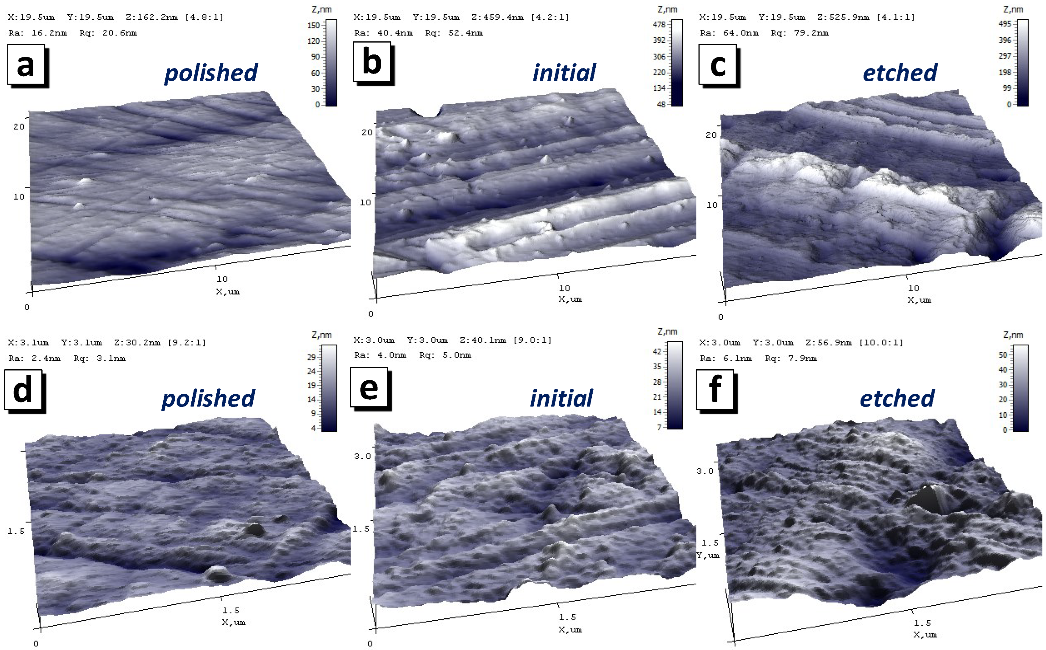
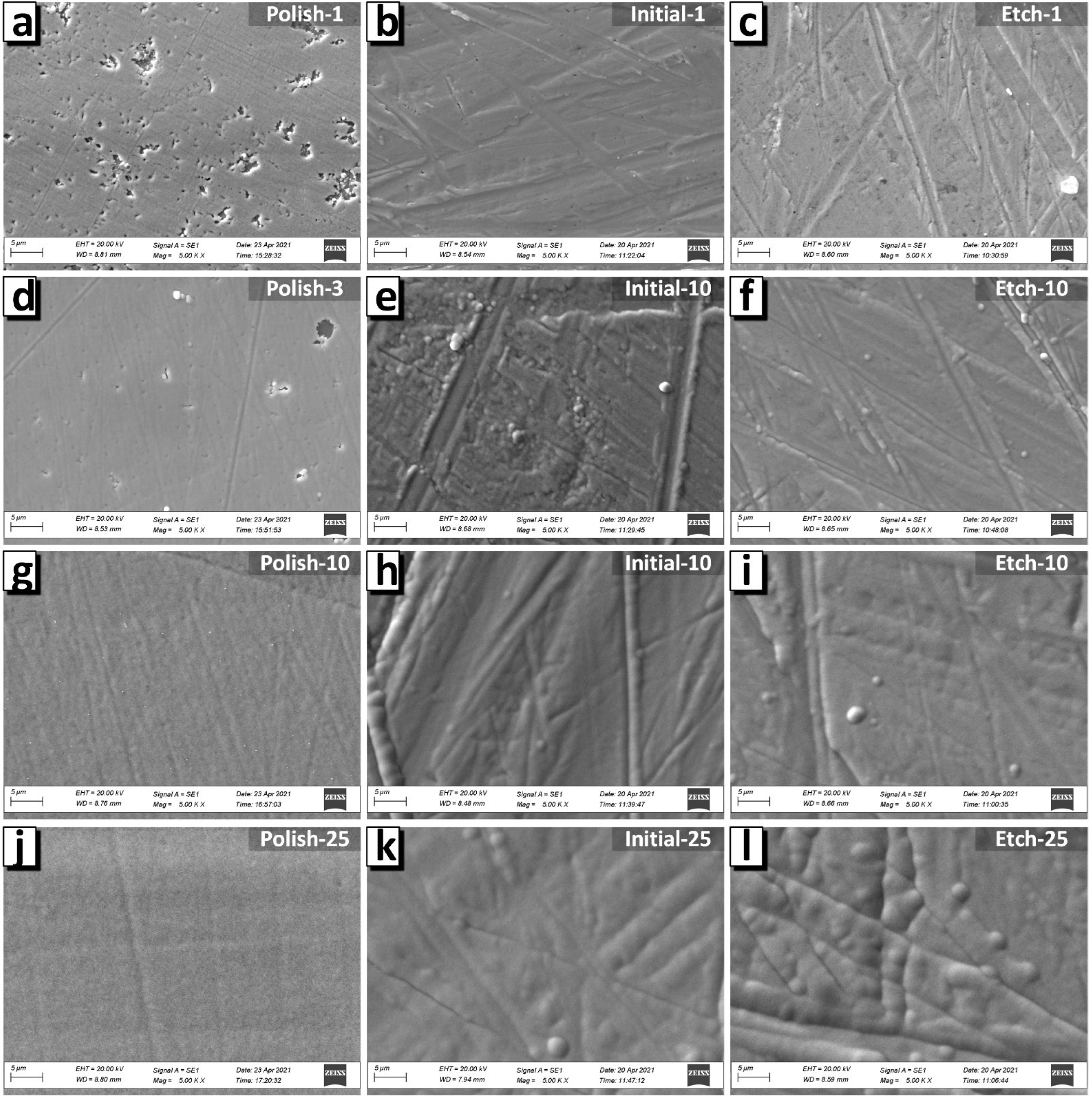
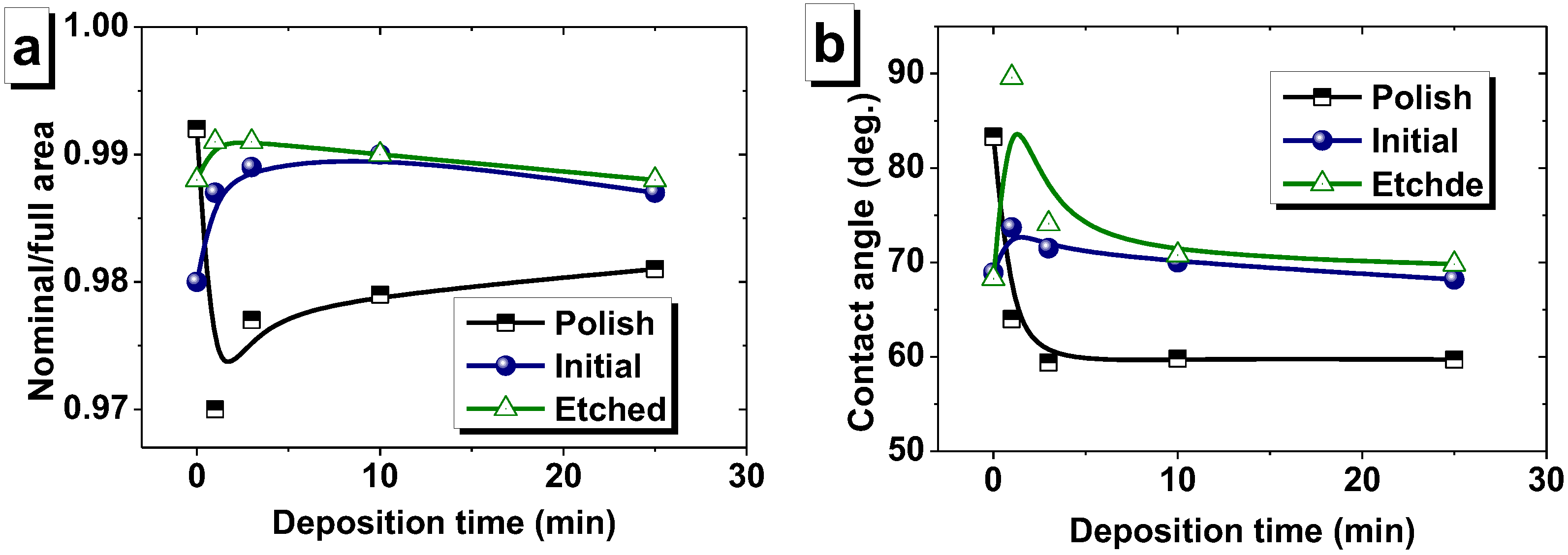
3.1. Surface Structure and Properties of the Substrates

The method of the surface preparation of the substrates can have a significant effect on adhesion between the substrate and the electrodeposited film. Particular attention should be paid to the adhesion between the substrate and the film in case of deposition on a polished surface. Adhesion tests by the lattice pattern method were carried out for all samples. The adhesion test results, in accordance with the Russian standard GOST 9.302-88 and American standard ASTM D 3359-09, showed that all samples had no peeling, removal, cracking, etc., with 0% area removed, and the edges of the cuts were completely smooth.
Figure 2 shows AFM images of the three substrate types used at different magnifications (sizes of images are 20 × 20 µm2 (a–c) and 3 × 3 µm2 (d–f)), including for substrates polished with subsequent mild etching (a,d), after mild etching or initial substrate (b,e) and after intensive etching (c,f). The figure clearly shows that polishing followed by mild etching (Figure 2a,d) made the surface more uniform and smoother compared to the other samples. Table 2 shows the main substrate parameters used for deposition. It is important to distinguish between roughness levels. The surface roughness determined in a 3 × 3 µm2 area will differ from the roughness in a 20 × 20 µm2 area. For simplicity’s sake, the terms “nano-roughness” and “micro-roughness” will be used. The values of nano-roughness are always less than microroughness values [62]. The microroughness of the polished substrate was 22 nm, and the initial and etched micro-roughnesses were 100 and 83 nm, respectively. The nano-roughness of the polished substrate was 2.1 nm, and the initial and etched micro-roughnesses were 4.4 and 6.1 nm, respectively. The discrepancy between the values of micro- and nano-roughness is a consequence of the different nature of these parameters. In the case considered here, micro-roughness was determined by the depth of the grinding and polishing grooves and surface waviness; nano-roughness was determined by the configuration of nanosized grains on the surface of the samples.
An equally important parameter for the substrate electrodeposition is the ratio of the nominal area to the full area (RN/F) [60]. The ratio RN/F allows for an estimation of the nature of the potential distribution on the surface during the reduction of metal ions on the substrate during electrodeposition. The lowest value of the RN/F = 0.980 corresponds to the substrate that was subjected only to mild etching (initial). Conversely, after mechanical polishing, the substrate had the ratio closest to one (0.992). It was determined in an area of 20 × 20 µm2. Thus, the same value of the current strength set by the equipment during deposition for these substrates will lead to different values of the actual current density on the surface. The lowest current density will correlate to the initial substrate, and the highest will correlate to the polished substrate.
Another important substrate characteristic is wettability, or the contact angle value. The results of the contact angle measurement (Table 2) show that the polished substrate exhibited hydrophobic behavior concerning the electrolyte (contact angle = 83°), while other substrates (after mild and intensive etching) were more hydrophilic (contact angles were in range 68–69°). Specific surface energy (SSE) is closely related to wettability and is in agreement with it. As shown in Table 2, the SSE of the polished Cu substrate was 0.18 N/m, and after mild and intensive etching, the substrates had similar values of specific surface energy equal to 0.26 and 0.27 N/m, respectively.

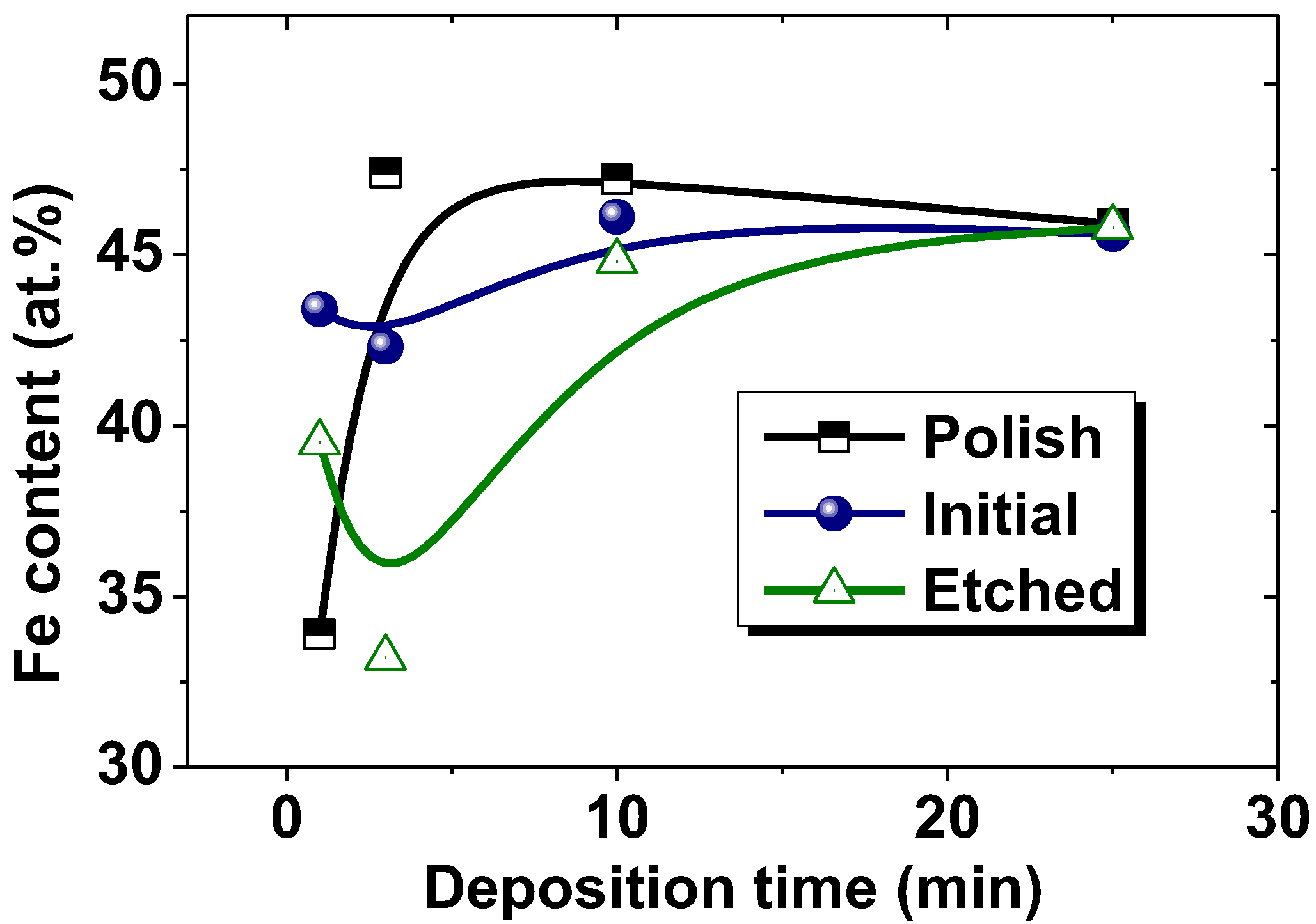
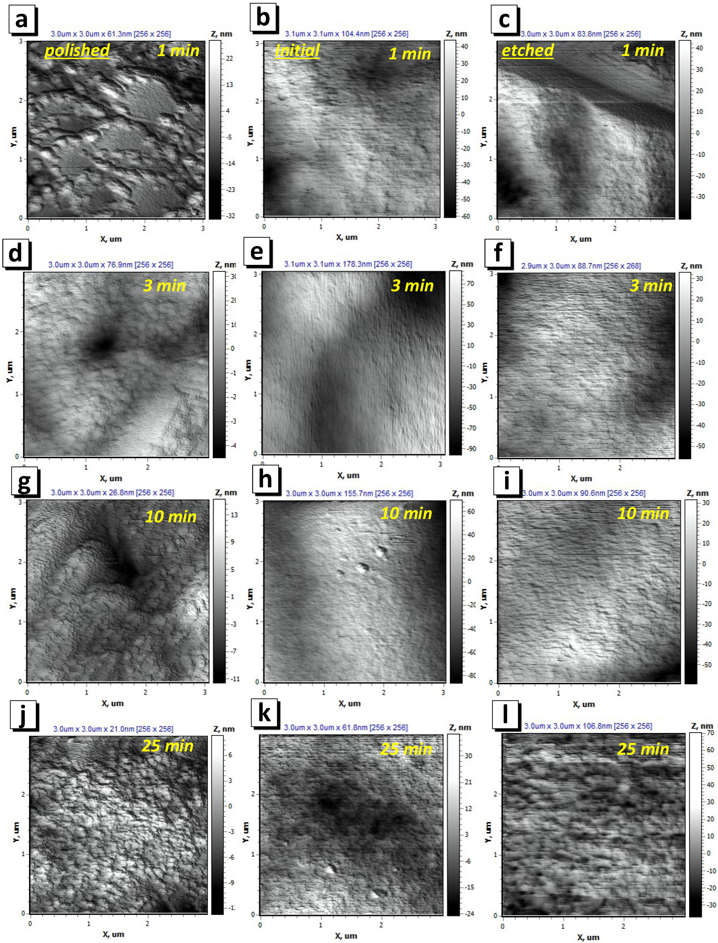
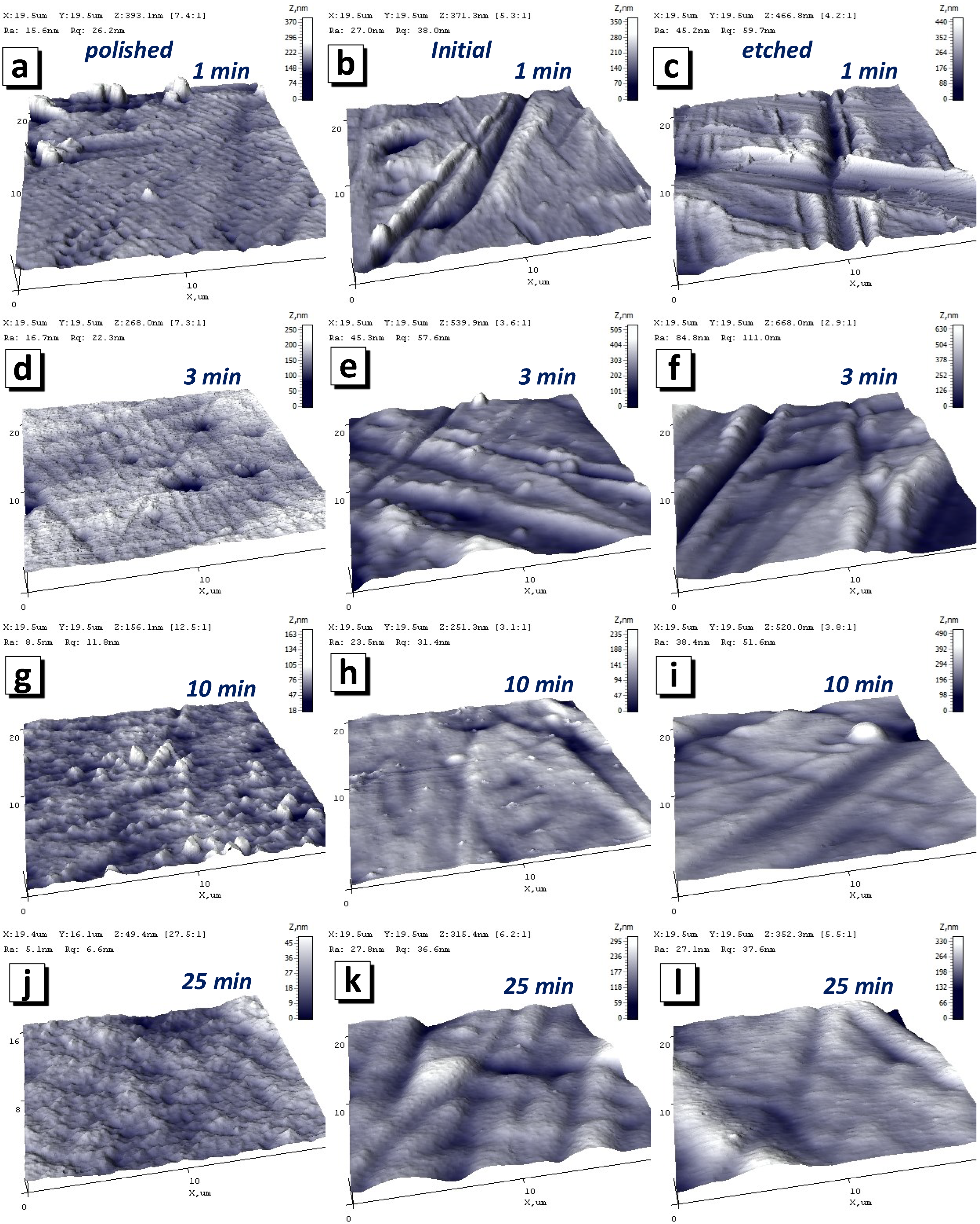
3.2. Surface Structure and Properties of the NiFe Films

The deposition was carried out in a galvanostatic mode, and the voltage change during deposition can be observed in Figure 1. An increase in potential followed by a decrease to a constant value is a common phenomenon in the electrodeposition of binary and ternary alloys from complex electrolytes [43,63]. During the first stages of deposition (from 10s of seconds to 3–5 min), the potential increases due to an increase in the electrolyte resistance and a higher potential for the discharge of metal ions onto the substrate material. In addition, the growth of the potential is due to the difficult diffusion of heavy metal ions to the cathode. The decrease in the deposition potential is indicative of a change in the deposition kinetics in this region under the influence of a number of competing factors. After the extremum is reached, deposition occurs on a fully formed film, and the discharge potential decreases. This also affects the formation of complexes from simple salts in the electrolyte solution and the diffusion of ions to the cathode. As a result, the resistance of the electrolyte becomes low, the potential reaches a minimum and remains constant, and the deposition process is in equilibrium.
The thickness of the Ni-Fe films obtained within 1 min was about 300–400 nm. Films with a thickness of 1.0–1.2 µm were formed in 3 min, 3.5–3.7 µm in 10 min of growth and about 9 µm in 25 min.
Table 3 demonstrates results of XRD investigations of the NiFe films obtained on the different substrates during 25 min. The XRD study verified that all films were well-described by a cubic-face-centered structure, with a space group Fm-3m (No. 225). The parameter and unit cell volume of the NiFe film obtained on a polished substrate were 3.570 Å and 45.499 Å3, respectively. The parameters and volumes of the films obtained on the initial and etched substrates were equal to each other and amounted to 3.372 Å and 45.576 Å3. The smaller size of the unit cell of Polish-25 film may have been a consequence of the surface compression of nanosized crystallites. As the results show (see Table 3), the coherent scattering region (CSR) for the Polish-25 sample was 5.3 nm, while it was 6.1 and 6.0 nm for the Initial-25 and Etch-25 samples. For the same reason (surface compression of crystallites), an increase in internal microstrain was observed for the Polish-25 samples (0.39 %) as compared to the Initial-25 (0.28 %) and Etch-25 (0.29 %) samples.
Figure 3 shows the change in the iron content in the NiFe films depending on the deposition time. It should be noted that the data show the composition on the film surface rather than the entire volume, as was achieved in EDX studies due to the low value of the accelerating voltage (5 kV) during investigation.
The NiFe films obtained within 1 min on polished, initial and etched substrates had an iron content of 33.9, 43.4 and 39.5 at.%, respectively (Figure 3). This can be fully explained by the influence of the structure and surface properties of the substrates. The polished substrate had the lowest roughness, a high ratio of the nominal to the full area and was highly hydrophobic (see Table 2). These characteristics, in combination, lead to the fact that the real surface area that was involved in the electrodeposition process was close to the nominal one (RN/F = 0.992). The opposite was seen for the substrate characteristics after mild etching (initial). The roughness values were much higher, and the contact angles were smaller (hydrophilic properties) (Table 2). The etched substrate had similar values of wettability and roughness. The etched, and especially the initial substrate, had a larger real surface area than the nominal one (RN/F = 0.980 for the initial substrate and RN/F = 0.988 for the etched substrate). The result of this is that the current density during electrodeposition was higher on the polished surface than on the initial and etched substrates. It is known that an increase in the current density leads to a decrease in the iron content in the film, which was described in [43,45]. In addition, the high surface roughness of the initial substrate (with a micro-roughness equal to 100 nm and nano-roughness equal to 4.6 nm) and etched substrate (with a micro-roughness equal to 83 nm and nano-roughness equal to 6.0 nm) prevented the removal of hydrogen from the cathode surface, which is actively released during the electrodeposition process. A high concentration of H+ ions lead to a decrease in the pH level in the cathode region, which leads to an increase in iron content. It is known that a decrease in the pH level leads to the formation of iron-rich films [43,45].
As a result, a rough structure with clearly visible grains 100–200 nm in size was formed on the surface of the polished substrate (Figure 4a). It is likely that island growth appeared on the film, which is a consequence of the poor wettability of the substrate. The AFM image (Figure 5a) and SEM image (Figure 6a) have a lower magnification and show that a film with pores was formed on the polished substrate within 1 min of electrodeposition. This led to the ratio of the nominal to the full area (0.970) (Figure 7a). The grain structure of the surface naturally led to a decrease in the contact wetting angle from 83.3 to 54.0 deg. (Figure 7b). As a result, an increase in the iron content to 47.4 at.% (3 min) was observed with further film growth. With a further increase in the deposition time, the changes in wettability and RN/F were not significant, and their effect was compensated for, so the composition of the deposited films remained constant with an iron content of about 46–47 at%.
The behavior of the films growing on the initial and etched substrates was opposite. The micro- and nanoscale bumps of the substrates were quickly filled with nanosized grains, and within 1 min of growth, smooth films with low roughness had already formed on the initial and etched surface. Thus, the ratio of the nominal to the full area of the initial-1 film was 0.987, and that of the etched-1 film was 0.991. Low roughness and good surface uniformity led to poor wettability. The contact angle was 73.7 and 89.6 deg. for the inital-1 and etched-1 films, respectively. Thus, with further growth of the films (3 min), iron-depleted layers were formed, which can be seen in the graph of the dependence of the iron content on the deposition time (Figure 3) for the initial and etched substrates. Films obtained on initial and etched substrates within 3 min, in contrast to those obtained in 1 min, had grains with a size of 2–4 μm on the surface (Figure 5e,f and Figure 6e,f). The presence of grains caused some decrease in wettability, which in turn led to an increase in the iron content to 46.1 and 44.8 at % for the films on the initial and etched substrates, respectively, as described above.
The SEM and AFM images (Figure 4, Figure 5 and Figure 6) show no significant changes in the film surface structure with a further increase in the deposition time and film thickness. Additionally, the values of the wetting angle and RN/F did not change significantly with an increase in the deposition time from 3 to 25 min and the film thickness from 1.0–1.2 to 9 μm. Consequently, the composition of the films formed at a deposition time of more than 3 min remained unchanged.

4. Conclusions

NiFe films were electrolytically deposited onto Cu substrates, which were prepared for synthesis in various ways. As a result of different preparations, the substrates had different microstructure and surface properties. The study of the chemical composition gradient showed that the NiFe film obtained on a polished substrate had the lowest iron content (33.9 at.%), and the Fe concentration in the film increased to about 46–47 at.% for a film with a thickness of about 1 μm. Finally, the stoichiometry did not change during further growth on the polished substrate. NiFe films obtained on the initial substrate and the substrate after aggressive etching showed another behavior. At the first stages, the iron content in the film was 33.9 and 39.5 at.%, and then it decreased to its minimum. When the film thickness reached about 9 µm, the iron content in all samples was the same and equaled 46–47 at.%. Such anomalous behavior is explained by the complex and competing influence of the structure and properties of the surface. Firstly, the low ratio of the nominal area to the total area contributed to a decrease in the actual value of the current density. An increase in the current density led to a decrease in the iron content in the film. Secondly, the poor wettability of the substrates and the films already deposited by the electrolyte led to an increase in the current density and, consequently, to a decrease in the iron content. Finally, the high surface roughness prevented the removal of hydrogen from the cathode surface, which is actively released during the electrodeposition process. A high concentration of H+ ions led to a decrease in the pH level in the cathode region, which led to an increase in iron content. A decrease in the pH level led to the formation of iron-rich films.

Author Contributions

Synthesis of the samples, A.N.K. and M.I.P.; writing—original draft preparation, T.I.Z. and T.I.U.; investigation, O.D.K., V.A.F. and A.S.K.; resources and data curation, D.I.T.; supervision, A.V.T. and V.M.F.; review and editing, S.V.T. and A.V.N.; funding acquisition, M.U.K. and A.M.I. All authors have read and agreed to the published version of the manuscript.

Funding

Alex V. Trukhanov thanks the NUST MISIS for support within the framework of the «Priority 2030» (K6-2022-043).

Data Availability Statement

The data of the study are available upon reasonable request from the corresponding author.

Acknowledgments

The authors express their gratitude to the Research Center of Advanced Materials, King Khalid University, Saudi Arabia, for their support (award number KKU/RCAMS/22).

Conflicts of Interest

The authors declare no conflict of interest.

References

  1. Zhang, B.; Fenineche, N.E.; Zhu, L.; Liao, H.; Coddet, C. Studies of Magnetic Properties of Permalloy (Fe30%Ni) Prepared by SLM Technology. J. Magn. Magn. Mater. 2012, 324, 495–500. [Google Scholar] [CrossRef]
  2. Yi, J.B.; Li, X.P.; Ding, J.; Seet, H.L. Study of the Grain Size, Particle Size and Roughness of Substrate in Relation to the Magnetic Properties of Electroplated Permalloy. J. Alloys Compd. 2007, 428, 230–236. [Google Scholar] [CrossRef]
  3. Svalov, A.V.; Aseguinolaza, I.R.; Garcia-Arribas, A.; Orue, I.; Barandiaran, J.M.; Alonso, J.; Fernández-Gubieda, M.L.; Kurlyandskaya, G.V. Structure and Magnetic Properties of Thin Permalloy Films near the Transcritical State. IEEE Trans. Magn. 2010, 46, 333–336. [Google Scholar] [CrossRef]
  4. Mazeeva, A.K.; Staritsyn, M.V.; Bobyr, V.V.; Manninen, S.A.; Kuznetsov, P.A.; Klimov, V.N. Magnetic Properties of Fe–Ni Permalloy Produced by Selective Laser Melting. J. Alloys Compd. 2020, 814, 152315. [Google Scholar] [CrossRef]
  5. Sharko, S.A.; Serokurova, A.I.; Zubar, T.I.; Trukhanov, S.V.; Tishkevich, D.I.; Samokhvalov, A.A.; Kozlovskiy, A.L.; Zdorovets, M.V.; Panina, L.V.; Fedosyuk, V.M.; et al. Multilayer Spin-Valve CoFeP/Cu Nanowires with Giant Magnetoresistance. J. Alloys Compd. 2020, 846, 156474. [Google Scholar] [CrossRef]
  6. Trukhanov, A.V.; Grabchikov, S.S.; Solobai, A.A.; Tishkevich, D.I.; Trukhanov, S.V.; Trukhanova, E.L. Journal of Magnetism and Magnetic Materials AC and DC-Shielding Properties for the Ni80Fe20/Cu Film Structures. J. Magn. Magn. Mater. 2017, 443, 142–148. [Google Scholar] [CrossRef]
  7. Grabchikov, S.S.; Trukhanov, A.V.; Trukhanov, S.V.; Kazakevich, I.S.; Solobay, A.A.; Erofeenko, V.T.; Vasilenkov, N.A.; Volkova, O.S.; Shakin, A. Effectiveness of the Magnetostatic Shielding by the Cylindrical Shells. J. Magn. Magn. Mater. 2016, 398, 49–53. [Google Scholar] [CrossRef]
  8. Kubo, E.; Ooi, N.; Aoki, H.; Watanabe, D.; Jeong, J.H.; Kimura, C.; Sugino, T. Effect of Magnetic Field on Permeability of Electroplated Permalloy for Microdevices. Jpn. J. Appl. Phys. 2010, 49, 5–8. [Google Scholar] [CrossRef]
  9. Koo, B.; Yoo, B. Electrodeposition of Low-Stress NiFe Thin Films from a Highly Acidic Electrolyte. Surf. Coat. Technol. 2010, 205, 740–744. [Google Scholar] [CrossRef]
  10. Cooper, E.I.; Bonhôte, C.; Heidmann, J.; Hsu, Y.; Kern, P.; Lam, J.W.; Ramasubramanian, M.; Robertson, N.; Romankiw, L.T.; Xu, H. Recent Developments in High-Moment Electroplated Materials for Recording Heads. IBM J. Res. Dev. 2005, 49, 103–126. [Google Scholar] [CrossRef]
  11. Osaka, T.; Asahi, T.; Kawaji, J.; Yokoshima, T. Development of High-Performance Magnetic Thin Film for High-Density Magnetic Recording. Electrochim. Acta 2005, 50, 4576–4585. [Google Scholar] [CrossRef]
  12. Almessiere, M.A.; Trukhanov, A.V.; Slimani, Y.; You, K.Y.; Trukhanov, S.V.; Trukhanova, E.L.; Esa, F.; Sadaqati, A.; Chaudhary, K.; Zdorovets, M.; et al. Correlation between Composition and Electrodynamics Properties in Nanocomposites Based on Hard/Soft Ferrimagnetics with Strong Exchange Coupling. Nanomaterials 2019, 9, 202. [Google Scholar] [CrossRef] [PubMed]
  13. Dastagir, T.; Xu, W.; Sinha, S.; Wu, H.; Cao, Y.; Yu, H. Tuning the Permeability of Permalloy Films for On-Chip Inductor Applications. Appl. Phys. Lett. 2010, 97, 10–13. [Google Scholar] [CrossRef]
  14. O’Donnell, T.; Wang, N.; Kulkarni, S.; Meere, R.; Rhen, F.M.F.; Roy, S.; O’Mathuna, S.C. Electrodeposited Anisotropic NiFe 45/55 Thin Films for High-Frequency Micro-Inductor Applications. J. Magn. Magn. Mater. 2010, 322, 1690–1693. [Google Scholar] [CrossRef]
  15. Jiang, C.; Xue, D.; Sui, W. Broadband Microwave Absorption in [NiFe/FeMn]n Exchange-Coupled Multilayer Films. Thin Solid Film. 2011, 519, 2527–2530. [Google Scholar] [CrossRef]
  16. Trukhanov, A.V.; Kostishyn, V.G.; Panina, L.V.; Korovushkin, V.V.; Turchenko, V.A.; Thakur, P.; Thakur, A.; Yang, Y.; Vinnik, D.A.; Yakovenko, E.S.; et al. Control of Electromagnetic Properties in Substituted M-Type Hexagonal Ferrites. J. Alloys Compd. 2018, 754, 247–256. [Google Scholar] [CrossRef]
  17. Kuanr, B.K.; Marson, R.; Mishra, S.R.; Kuanr, A.V.; Camley, R.E.; Celinski, Z.J. Gigahertz Frequency Tunable Noise Suppressor Using Nickel Nanorod Arrays and Permalloy Films. J. Appl. Phys. 2009, 105, 9–12. [Google Scholar] [CrossRef]
  18. Tong, Q.; Liu, F.; Xiao, J.; Yao, W. Skyrmions in the Moiré of van Der Waals 2D Magnets. Nano Lett. 2018, 18, 7194–7199. [Google Scholar] [CrossRef] [PubMed]
  19. Vorobjova, A.I.; Tishkevich, D.I.; Outkina, E.A.; Shimanovich, D.L.; Razanau, I.U.; Zubar, T.I.; Bondaruk, A.A.; Zheleznova, E.K.; Dong, M.; Aloraini, D.A.; et al. A Study of Ta2O5 Nanopillars with Ni Tips Prepared by Porous Anodic Alumina Through-Mask Anodization. Nanomaterials 2022, 12, 1344. [Google Scholar] [CrossRef]
  20. Tishkevich, D.I.; Vorobjova, A.I.; Vinnik, D.A. Template Assisted Ni Nanowires Fabrication. Mater. Sci. Forum 2019, 946, 235–241. [Google Scholar] [CrossRef]
  21. Zubar, T.; Fedosyuk, V.; Tishkevich, D.; Kanafyev, O.; Astapovich, K.; Kozlovskiy, A.; Zdorovets, M.; Vinnik, D.; Gudkova, S.; Kaniukov, E.; et al. The E Ff Ect of Heat Treatment on the Microstructure and Mechanical Properties of 2D Nanostructured Au/NiFe System. Nanomaterials 2020, 10, 1077. [Google Scholar] [CrossRef] [PubMed]
  22. Vorobjova, A.; Tishkevich, D.; Shimanovich, D.; Zdorovets, M.; Kozlovskiy, A.; Zubar, T.; Vinnik, D.; Dong, M.; Trukhanov, S.; Trukhanov, A.; et al. Electrochemical Behaviour of Ti/Al2O3/Ni Nanocomposite Material in Artificial Physiological Solution: Prospects for Biomedical Application. Nanomaterials 2020, 10, 173. [Google Scholar] [CrossRef] [PubMed]
  23. Tishkevich, D.I.; Grabchikov, S.S.; Lastovskii, S.B.; Trukhanov, S.V.; Vasin, D.S.; Zubar, T.I.; Kozlovskiy, A.L.; Zdorovets, M.V.; Sivakov, V.A.; Muradyan, T.R.; et al. Function Composites Materials for Shielding Applications: Correlation between Phase Separation and Attenuation Properties. J. Alloys Compd. 2019, 771, 238–245. [Google Scholar] [CrossRef]
  24. Tishkevich, D.I.; Grabchikov, S.S.; Grabchikova, E.A.; Vasin, D.S.; Lastovskiy, S.B.; Yakushevich, A.S.; Vinnik, D.A.; Zubar, T.I.; Kalagin, I.V.; Mitrofanov, S.V.; et al. Modeling of paths and energy losses of high-energy ions in single-layered and multilayered materials. IOP Conf. Ser. Mater. Sci. Eng. 2020, 848, 012089. [Google Scholar] [CrossRef]
  25. Zubar, T.; Grabchikov, S.; Kotelnikova, A.; Kaniukov, E.; Kutuzau, M.; Leistner, K.; Nielsch, K.; Vershinina, T.; Tishkevich, D.; Kanafyev, O.; et al. Efficiency of Magnetostatic Protection Using Nanostructured Permalloy Shielding Coatings Depending on Their Microstructure. Nanomaterials 2021, 11, 634. [Google Scholar] [CrossRef]
  26. Almessiere, M.A.; Slimani, Y.; Güngüneş, H.; Ali, S.; Manikandan, A.; Ercan, I.; Baykal, A.; Trukhanov, A.V. Magnetic Attributes of NiFe2O4 Nanoparticles:Influence of Dysprosium Ions (Dy3+) Substitution. Nanomaterials 2019, 11, 1–25. [Google Scholar]
  27. Cortes, M.; Peng, T.; Woytasik, M.; Moulin, J. Shape Anisotropy in Magneto-Impedance NiFe-Based Microsensors. J. Electrochem. Soc. 2015, 162, B129–B132. [Google Scholar] [CrossRef]
  28. Zubar, T.; Trukhanov, A.; Vinnik, D.; Astapovich, K.; Tishkevich, D.; Kaniukov, E.; Kozlovskiy, A.; Zdorovets, M.; Trukhanov, S. Features of the Growth Processes and Magnetic Domain Structure of NiFe Nano-Objects. J. Phys. Chem. C 2019, 123, 26957–26964. [Google Scholar] [CrossRef]
  29. Trukhanov, S.V.; Trukhanov, A.V.; Turchenko, V.A.; Trukhanov, A.V.; Trukhanova, E.L.; Tishkevich, D.I.; Ivanov, V.M.; Zubar, T.I.; Salem, M.; Kostishyn, V.G.; et al. Polarization Origin and Iron Positions in Indium Doped Barium Hexaferrites. Ceram. Int. 2018, 44, 290–300. [Google Scholar] [CrossRef]
  30. Biswal, A.; Panda, P.K.; Panda, P.K.; Acharya, A.N.; Tripathy, B.C.; Tripathy, B.C.; Alenazey, F.; Jiang, Z.T.; Minakshi Sundaram, M. Tuning the Morphology and Redox Behaviour by Varying the Concentration of Fe in a CoNiFe Ternary Oxide Heterostructure for Hybrid Devices. New J. Chem. 2020, 44, 9921–9932. [Google Scholar] [CrossRef]
  31. Wickramaarachchi, K.; Minakshi, M. Consequences of Electrodeposition Parameters on the Microstructure and Electrochemical Behavior of Electrolytic Manganese Dioxide (EMD) for Supercapacitor. Ceram. Int. 2022, 48, 19913–19924. [Google Scholar] [CrossRef]
  32. Biswal, A.; Panda, P.K.; Acharya, A.N.; Mohapatra, S.; Swain, N.; Tripathy, B.C.; Jiang, Z.T.; Minakshi Sundaram, M. Role of Additives in Electrochemical Deposition of Ternary Metal Oxide Microspheres for Supercapacitor Applications. ACS Omega 2020, 5, 3405–3417. [Google Scholar] [CrossRef] [PubMed]
  33. Zubar, T.I.; Panina, L.V.; Kovaleva, N.N.; Sharko, S.A.; Tishkevich, D.I. Anomalies in Growth of Electrodeposited Ni–Fe Nanogranular Films. CrystEngComm 2018, 20, 2306–2315. [Google Scholar] [CrossRef]
  34. Gong, J.; Riemer, S.; Venkatasamy, V.; Kautzky, M.; Tabakovic, I. Composition Gradients and Magnetic Properties of 10–100nm NiFe and CoFe Films Obtained by Electrodeposition. ECS Meet. Abstr. 2012, MA2012-02, 3398. [Google Scholar] [CrossRef]
  35. Gong, J.; Riemer, S.; Kautzky, M.; Tabakovic, I. Composition Gradient, Structure, Stress, Roughness and Magnetic Properties of 5–500 Nm Thin NiFe Films Obtained by Electrodeposition. J. Magn. Magn. Mater. 2016, 398, 64–69. [Google Scholar] [CrossRef]
  36. Vinnik, D.A.; Podgornov, F.V.; Zabeivorota, N.S.; Trofimov, E.A.; Zhivulin, V.E.; Chernukha, A.S.; Gavrilyak, M.V.; Gudkova, S.A.; Zherebtsov, D.A.; Ryabov, A.V.; et al. Effect of Treatment Conditions on Structure and Magnetodielectric Properties of Barium Hexaferrites. J. Magn. Magn. Mater. 2020, 498, 166190. [Google Scholar] [CrossRef]
  37. Gong, J.; Riemer, S.; Morrone, A.; Venkatasamy, V.; Kautzky, M.; Tabakovic, I. Composition Gradients and Magnetic Properties of 5–100 Nm Thin CoNiFe Films Obtained by Electrodeposition. J. Electrochem. Soc. 2012, 159, D447–D454. [Google Scholar] [CrossRef]
  38. Henstock, M.E.; Spencer-Timms, E.S. The Composition of Thin Electrodeposited Alloy Films with Special Reference to Nickel-Iron. Trans. IMF 1964, 42, 174–181. [Google Scholar] [CrossRef]
  39. Liu, X.; Zangari, G.; Shen, L. Electrodeposition of Soft, High Moment Co-Fe-Ni Thin Films. J. Appl. Phys. 2000, 87, 5410–5412. [Google Scholar] [CrossRef]
  40. Zubar, T.I.; Sharko, S.A.; Tishkevich, D.I.; Kovaleva, N.N.; Vinnik, D.A.; Gudkova, S.A.; Trukhanova, E.L.; Trofimov, E.A.; Chizhik, S.A.; Panina, L.V.; et al. Anomalies in Ni-Fe Nanogranular Films Growth. J. Alloys Compd. 2018, 748, 970–978. [Google Scholar] [CrossRef]
  41. Trukhanov, S.V.; Trukhanov, A.V.; Turchenko, V.A.; Kostishin, V.G.; Panina, L.V.; Kazakevich, I.S.; Balagurov, A.M. Crystal Structure and Magnetic Properties of the BaFe12−xInxO19 (x=0.1−1.2) Solid Solutions. J. Magn. Magn. Mater. 2016, 417, 130–136. [Google Scholar] [CrossRef]
  42. Kuznetsova, T.A.; Zubar, T.I.; Lapitskaya, V.A.; Sudzilouskaya, K.A.; Chizhik, S.A.; Didenko, A.L.; Svetlichnyi, V.M.; Vylegzhanina, M.E.; Kudryavtsev, V.V.; Sukhanova, T.E. Tribological Properties Investigation of the Thermoplastic Elastomers Surface with the AFM Lateral Forces Mode. In Proceedings of the IOP Conference Series: Materials Science and Engineering; IOP Publishing: Bristol, UK, 2017; Volume 256, p. 012022. [Google Scholar] [CrossRef]
  43. Bełtowska-Lehman, E.; Riesenkampf, A. Effect of the Electrode Supply Mode on the Chemical Composition Gradient of Permalloy Thin Films. Thin Solid Film. 1980, 71, 129–132. [Google Scholar] [CrossRef]
  44. Gao, L.Y.; Wan, P.; Liu, Z.Q. Gradient Growth of Fcc and Bcc Phase within FexNi1−x (50 < x < 75) Films during Direct-Current Wafer Electroplating. J. Magn. Magn. Mater. 2020, 498, 166131. [Google Scholar] [CrossRef]
  45. Eastham, D.R.; Boden, P.J.; Henstock, M.E. Factors Affecting the Composition Gradient in Electrodeposited Permalloy Films. Trans. IMF 1968, 46, 37–43. [Google Scholar] [CrossRef]
  46. Zubar, T.I.; Fedosyuk, V.M.; Trukhanov, A.V.; Kovaleva, N.N.; Astapovich, K.A.; Vinnik, D.A.; Trukhanova, E.L.; Kozlovskiy, A.L.; Zdorovets, M.V.; Solobai, A.A.; et al. Control of Growth Mechanism of Electrodeposited Nanocrystalline NiFe Films. J. Electrochem. Soc. 2019, 166, D173. [Google Scholar] [CrossRef]
  47. Luborsky, F.E. Influence of the Substrate and Electrolyte on the Composition and Properties of Thin Electrodeposited Ni-Fe Films. IEEE Trans. Magn. 1969, 5, 106–111. [Google Scholar] [CrossRef]
  48. Reekstin, J.P. Zero Magnetostriction Composition of NiFe Films. J. Appl. Phys. 1967, 38, 1449–1450. [Google Scholar] [CrossRef]
  49. Song, O.; Ballentine, C.A.; O’Handley, R.C. Giant Surface Magnetostriction in Polycrystalline Ni and NiFe Films. Appl. Phys. Lett. 1994, 64, 2593–2595. [Google Scholar] [CrossRef]
  50. Liao, S.H.; Anderson, S.E. Domain Characteristics and Conformal Deposition of NiFe Thin Films. J. Electrochem. Soc. 1993, 140, 208–211. [Google Scholar] [CrossRef]
  51. Konno, M.; Imamura, N. Magnetic Properteis of Fe-Ni Invar Alloy Films. J. Prysical Soc. Jpn. 1977, 42, 819–825. [Google Scholar] [CrossRef]
  52. Konno, M. Anomalius Thickness Dependence of Suturation Magnetization in Fe-Ni Invar Alloy Films Alloy Films. J. Prysical Soc. Jpn. 1983, 52, 1759–1764. [Google Scholar] [CrossRef]
  53. Zubar, T.I.; Trukhanov, A.V.; Vinnik, D.A. Influence of Surface Energy on Ni-Fe Thin Films Formation Process. Mater. Sci. Forum. 2019, 946, 228–234. [Google Scholar] [CrossRef]
  54. Zubar, T.I.; Fedosyuk, V.M.; Tishkevich, D.I.; Panasyuk, M.I.; Kanafyev, O.D.; Kozlovskiy, A.; Zdorovets, M.; Michels, D.; Lyakhov, D.; Trukhanov, A.V. Mechanisms of Elastoplastic Deformation and Their Effect on Hardness of Nanogranular Ni-Fe Coatings. Int. J. Mech. Sci. 2022, 215, 106952. [Google Scholar] [CrossRef]
  55. Warcholinski, B.; Gilewicz, A.; Kuprin, A.S.; Tolmachova, G.N.; Ovcharenko, V.D.; Kuznetsova, T.A.; Zubar, T.I.; Khudoley, A.L.; Chizhik, S.A. Mechanical Properties of Cr-O-N Coatings Deposited by Cathodic Arc Evaporation. Vacuum 2018, 156, 97–107. [Google Scholar] [CrossRef]
  56. Kuprin, A.S.; Kuznetsova, T.A.; Gilewicz, A.; Tolmachova, G.N.; Ovcharenko, V.D.; Abetkovskaia, S.O.; Zubar, T.I.; Khudoley, A.L.; Chizhik, S.A.; Lupicka, O.; et al. Tribological Properties of Vacuum Arc Cr-O-N Coatings in Macro- and Microscale. Probl. At. Sci. Technol. 2016, 106, 211–214. [Google Scholar]
  57. Warcholinski, B.; Gilewicz, A.; Kuznetsova, T.A.; Zubar, T.I.; Chizhik, S.A.; Abetkovskaia, S.O.; Lapitskaya, V.A. Mechanical Properties of Mo(C)N Coatings Deposited Using Cathodic Arc Evaporation. Surf. Coat. Technol. 2017, 319, 117–128. [Google Scholar] [CrossRef]
  58. Warcholinski, B.; Gilewicz, A.; Lupicka, O.; Kuprin, A.S.; Tolmachova, G.N.; Ovcharenko, V.D.; Kolodiy, I.V.; Sawczak, M.; Kochmanska, A.E.; Kochmanski, P.; et al. Structure of CrON Coatings Formed in Vacuum Arc Plasma Fluxes. Surf. Coat. Technol. 2017, 309, 920–930. [Google Scholar] [CrossRef]
  59. Warcholinski, B.; Kuznetsova, T.A.; Gilewicz, A.; Zubar, T.I.; Lapitskaya, V.A.; Chizhik, S.A.; Komarov, A.I.; Komarova, V.I.; Kuprin, A.S.; Ovcharenko, V.D.; et al. Structural and Mechanical Properties of Zr-Si-N Coatings Deposited by Arc Evaporation at Different Substrate Bias Voltages. J. Mater. Eng. Perform. 2018, 27, 3940–3950. [Google Scholar] [CrossRef]
  60. Kuznetsova, T.; Zubar, T.; Chizhik, S.; Gilewicz, A.; Lupicka, O.; Warcholinski, B. Surface Microstructure of Mo(C)N Coatings Investigated by AFM. J. Mater. Eng. Perform. 2016, 25, 5450–5459. [Google Scholar] [CrossRef]
  61. Zubar, T.I.; Fedosyuk, V.M.; Trukhanov, S.V.; Tishkevich, D.I.; Michels, D.; Lyakhov, D.; Trukhanov, A.V. Method of Surface Energy Investigation by Lateral AFM: Application to Control Growth Mechanism of Nanostructured NiFe Films. Sci. Rep. 2020, 10, 14411. [Google Scholar] [CrossRef]
  62. Zavaleyev, V.; Walkowicz, J.; Kuznetsova, T.; Zubar, T. The Dependence of the Structure and Mechanical Properties of Thin Ta-C Coatings Deposited Using Electromagnetic Venetian Blind Plasma Filter on Their Thickness. Thin Solid Film. 2017, 638, 153–158. [Google Scholar] [CrossRef]
  63. Tishkevich, D.I.; Vorobjova, A.I.; Vinnik, D.A. Formation and corrosion behavior of Nickel/Alumina nanocomposites. Solid State Phenom. 2020, 299, 100–106. [Google Scholar] [CrossRef]
Figure 1. Potential (black line) change during NiFe film synthesis in galvanostatic electrodeposition mode. The current was constant (blue line).
Nanomaterials 12 02926 g001
Figure 2. Three-dimensional AFM images of substrate surface topography after mechanical polishing (a,d), without special preparation or the initial substrate (b,e) and after mild chemical etching (c,f). The images sizes are 20 × 20 µm2 (ac) and 3 × 3 µm2 (df).
Nanomaterials 12 02926 g002
Figure 3. Iron concentration in NiFe films obtained on substrate after mechanical polishing (polish), without special preparation (initial) and after mild chemical etching (etch) depending on deposition time (1–25 min).
Nanomaterials 12 02926 g003
Figure 4. AFM images of topography of NiFe films on substrate after polishing (a,d,g,j), without special preparation or initial substrate (b,e,h,k) and after mild chemical etching (c,f,i,l). The deposition times were 1 min (ac), 3 min (df), 10 min (gi) and 25 min (jl). The images sizes are 3 × 3 µm2.
Nanomaterials 12 02926 g004
Figure 5. Three-dimensional AFM images of NiFe films on substrate after polishing (a,d,g,j), without special preparation or initial substrate (b,e,h,k) and after mild chemical etching (c,f,i,l). The deposition times were 1 min (ac), 3 min (df), 10 min (gi) and 25 min (jl). The images sizes are 20 × 20 µm2.
Nanomaterials 12 02926 g005
Figure 6. SEM images of the NiFe films on substrates with different roughnesses of substrate surface topography after polishing (a,d,g,j), without special preparation or initial substrate (b,e,h,k) and after chemical etching (c,f,i,l).
Nanomaterials 12 02926 g006
Figure 7. Ratio of nominal/full surface area (a) and contact angle (b) of NiFe films depending on deposition time.
Nanomaterials 12 02926 g007
Table 1. Features of substrate preparation, electrodeposition parameters and sample descriptions.
Short NameSubstrate MaterialSubstrate PreparationElectrolyte pH Electrolyte Temperature, °CCurrent Density, mA/cm2Deposition Time, min
Polish-1CuMechanical polishing, mild HCl etching (5 s)2.035251
Polish-33
Polish-1010
Polish-2525
Initial-1CuMild HCl etching (5 s)2.035251
Initial-33
Initial-1010
Initial-2525
Etch-1CuIntensive (NH4)2SO8 ammonium persulfate etching (60 s)2.035251
Etch-33
Etch-1010
Etch-2525
Table 2. Surface properties of Cu substrates with different preparation techniques.
SubstrateSubstrate
Micro-Roughness, nm
Substrate
Nano-Roughness, nm
RN/F *Contact Angle, °SSE **, N/m
Polished222.10.99283.30.18
Initial1004.60.98068.90.26
Etched836.00.98868.30.27
* RN/F is the ratio of the nominal to the full area, RN/F = 1 for atomically rough (ideal) surface. ** SSE is a specific surface energy obtained by AFM.
Table 3. Crystal structure parameters of NiFe films deposited on substrates after different preparations during 25 min.
SampleUnit Cell Parameter, a, ÅCell Volume V, Å3CSR *, nmMicrostrain, %
Polish-253.57045.4995.30.39
Initial-253.57245.5766.10.28
Etch-253.57245.5766.00.29
* CSR is the coherent scattering region.
Publisher’s Note: MDPI stays neutral with regard to jurisdictional claims in published maps and institutional affiliations.

