
Evolution in Lithography Techniques: Microlithography to Nanolithography

 and
and
Abstract
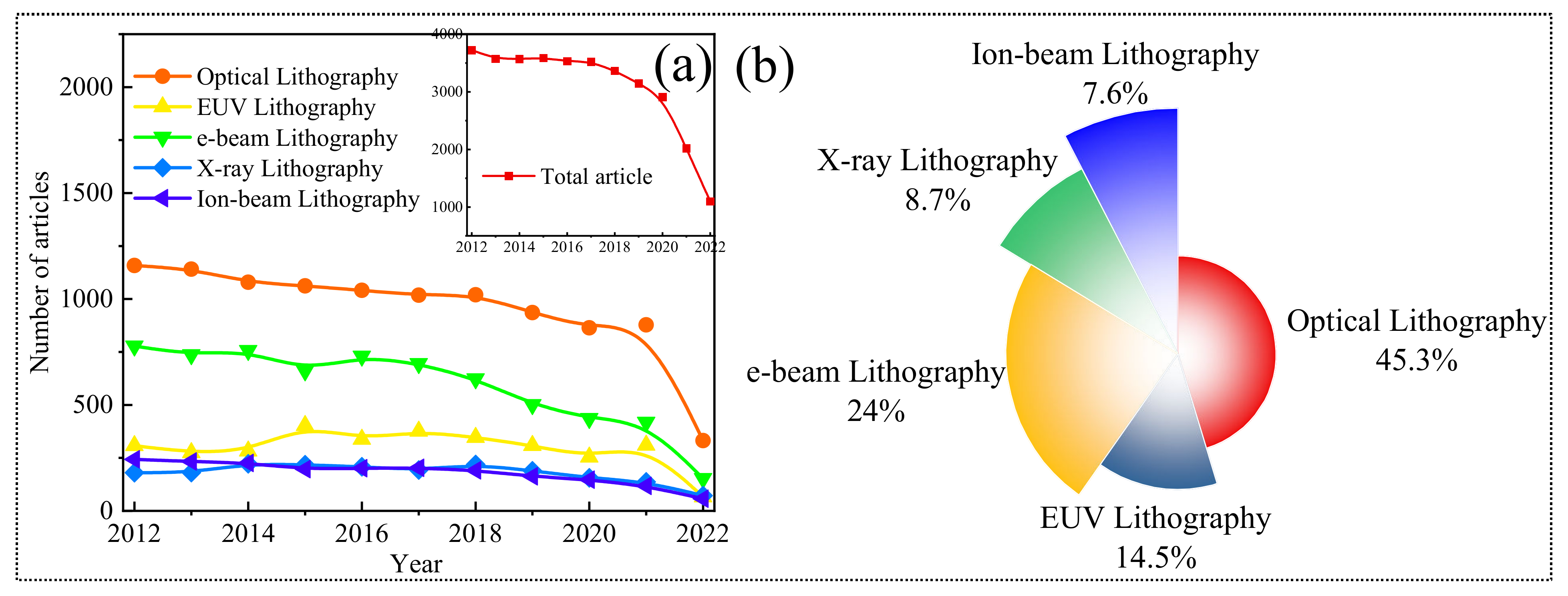
:1. Introduction
2. Optical Lithography
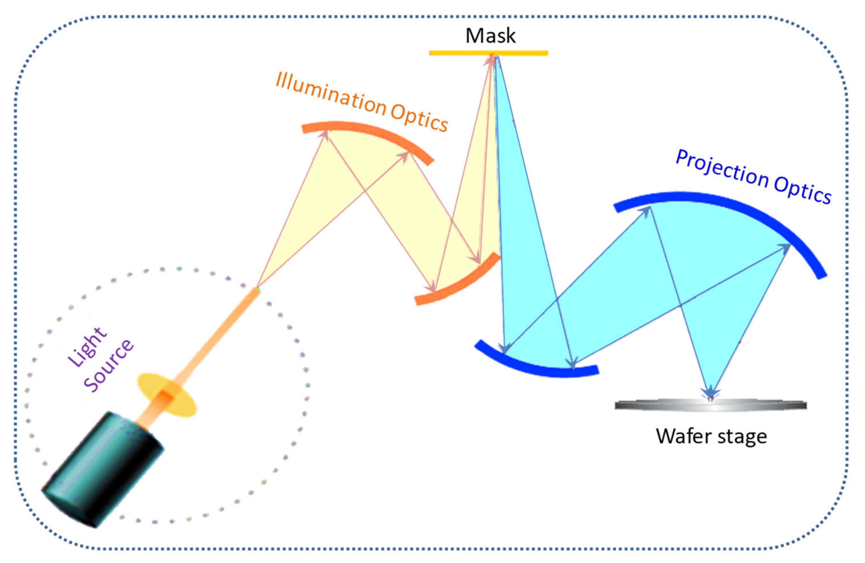
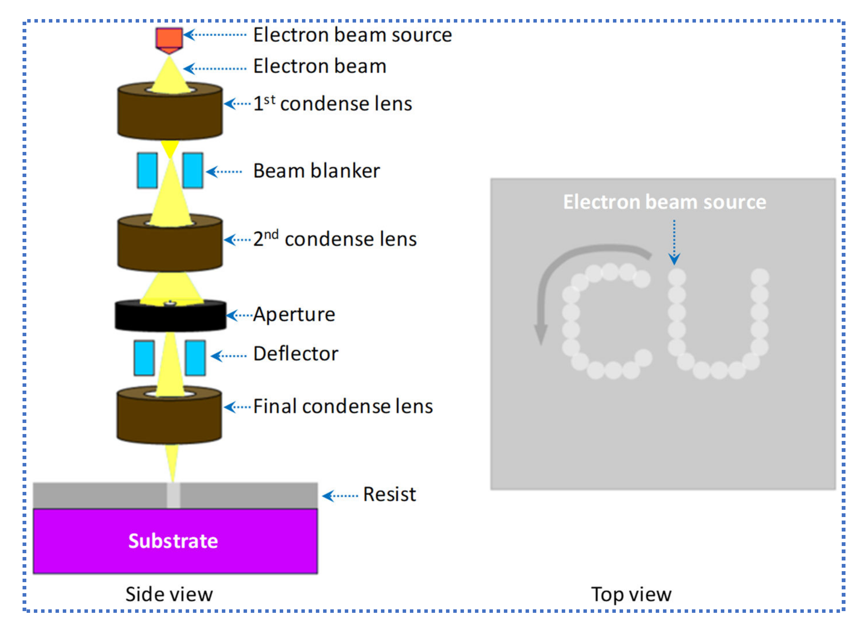
2.1. Exposure System
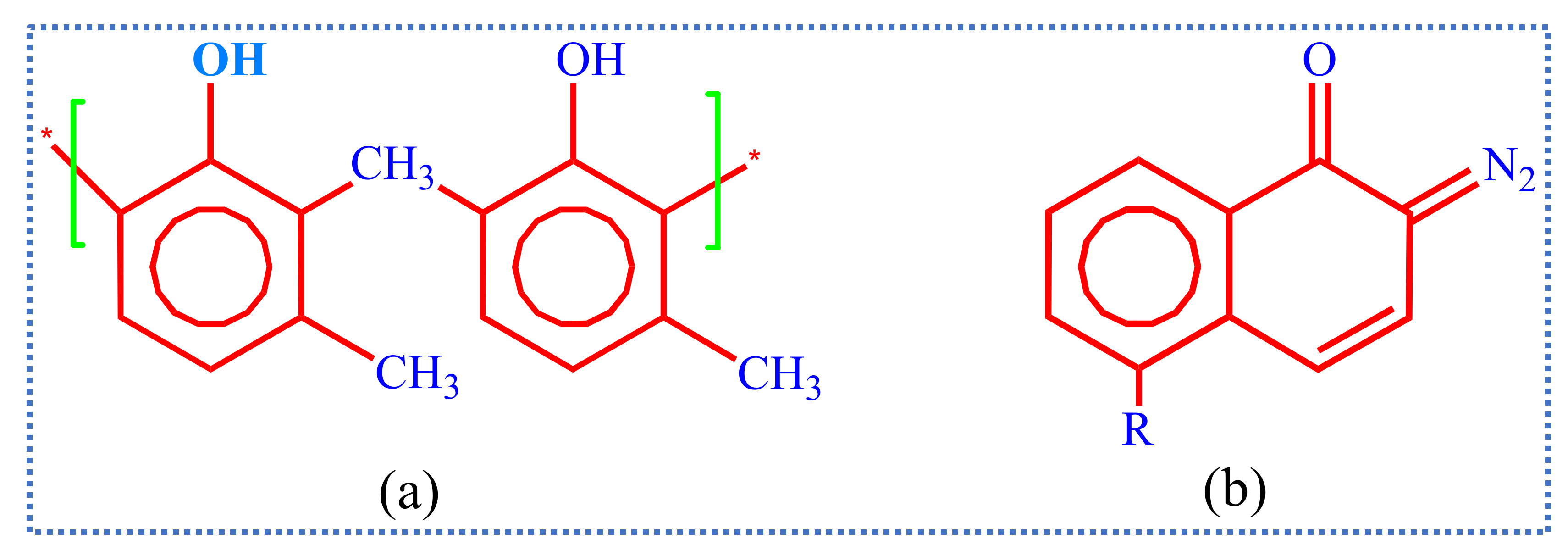
2.2. Resists
2.3. Limitations
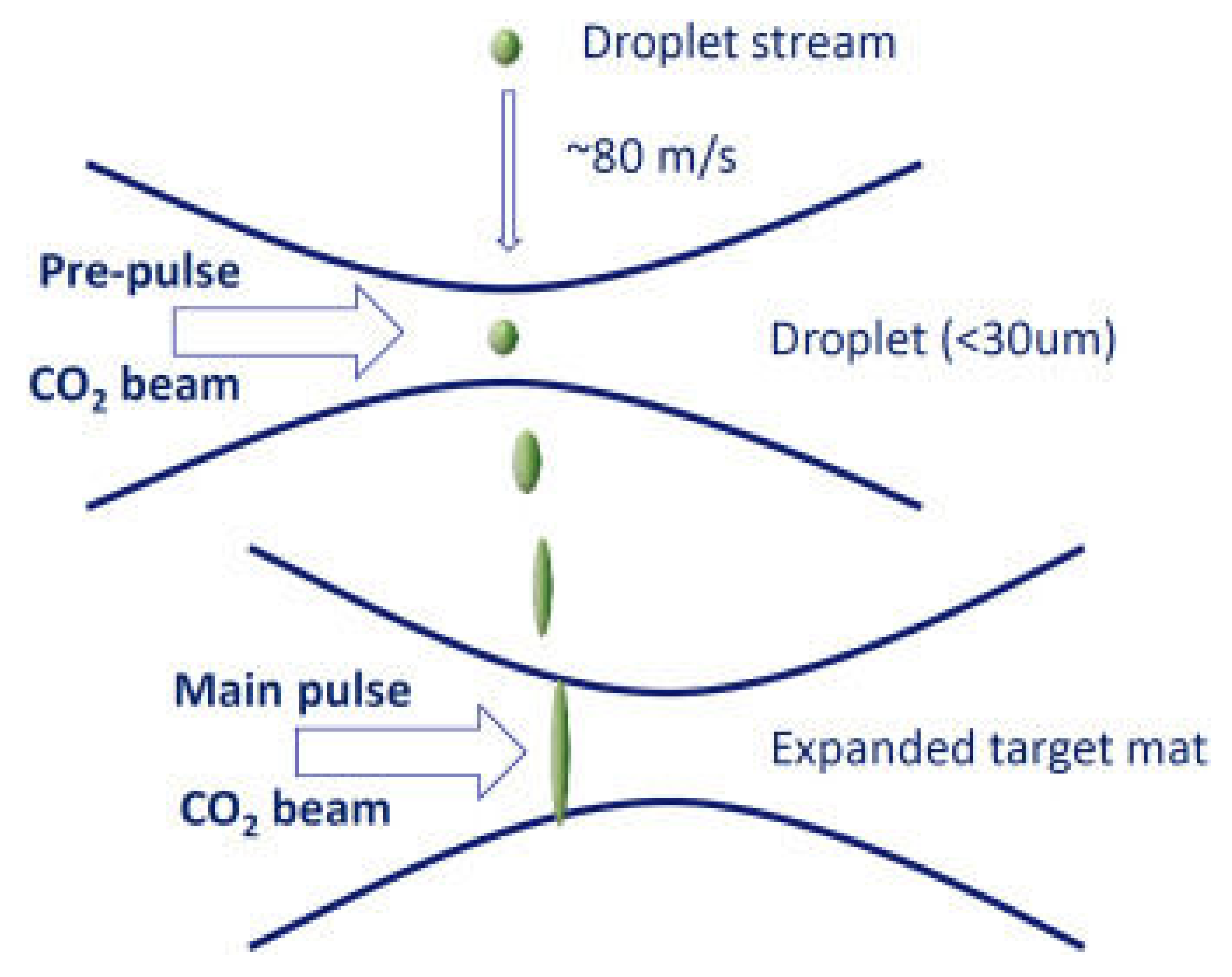
3. Extreme UV Lithography
3.1. Resist
Advancements in Resist Materials
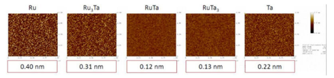
3.2. Mask
Advancement in Mask
3.3. Limitations
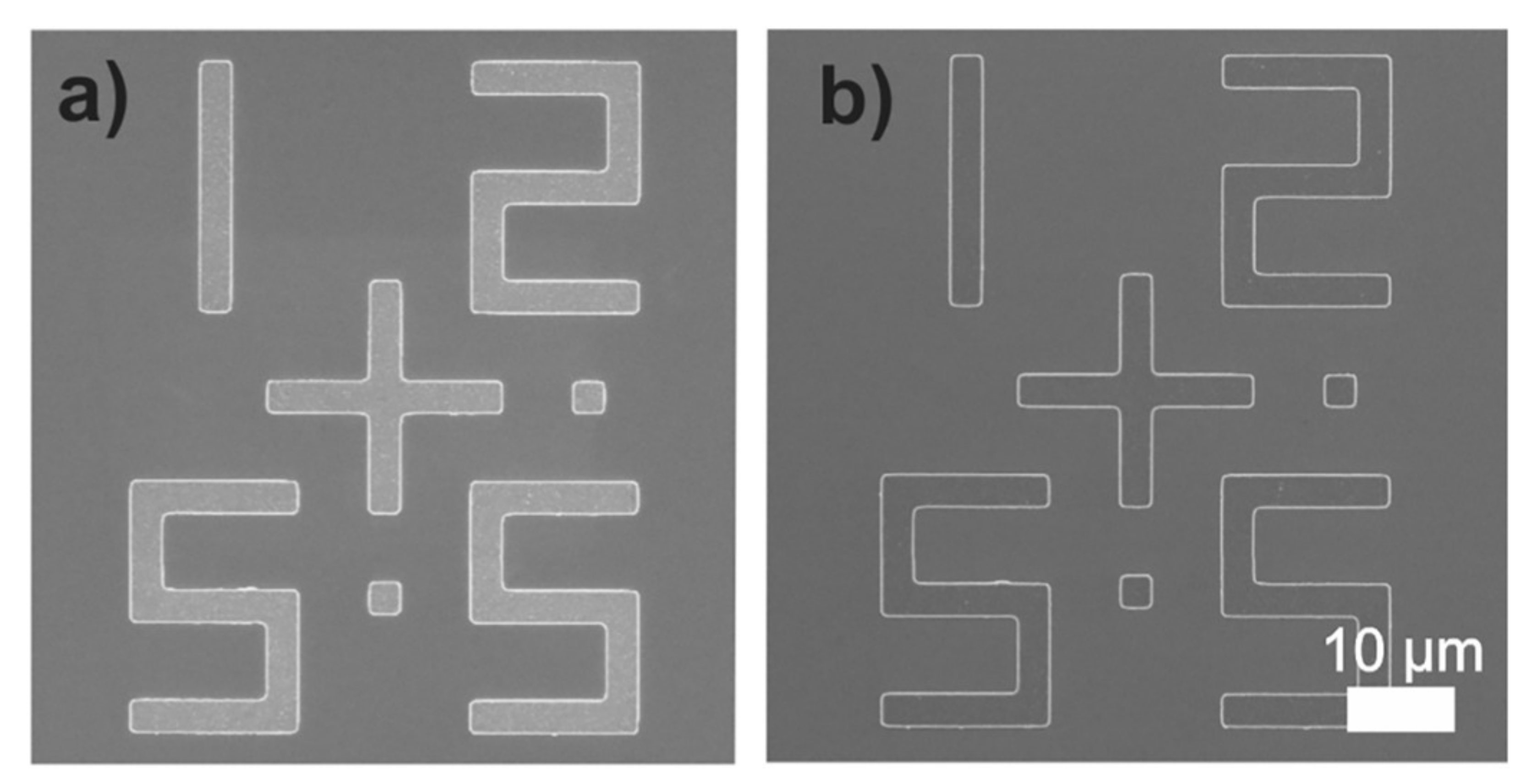
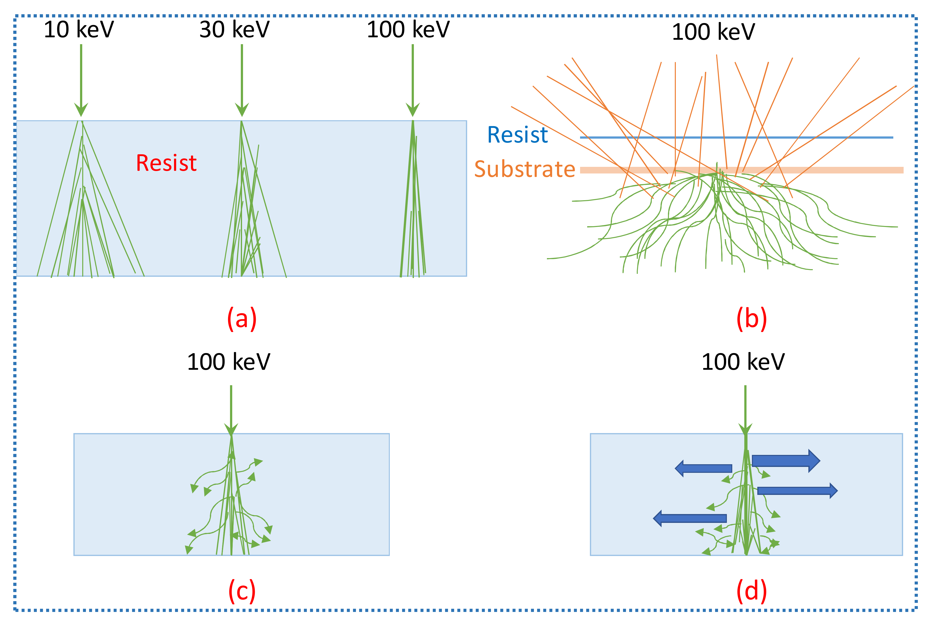
4. E-Beam Lithography
4.1. Resists
4.2. Limitations
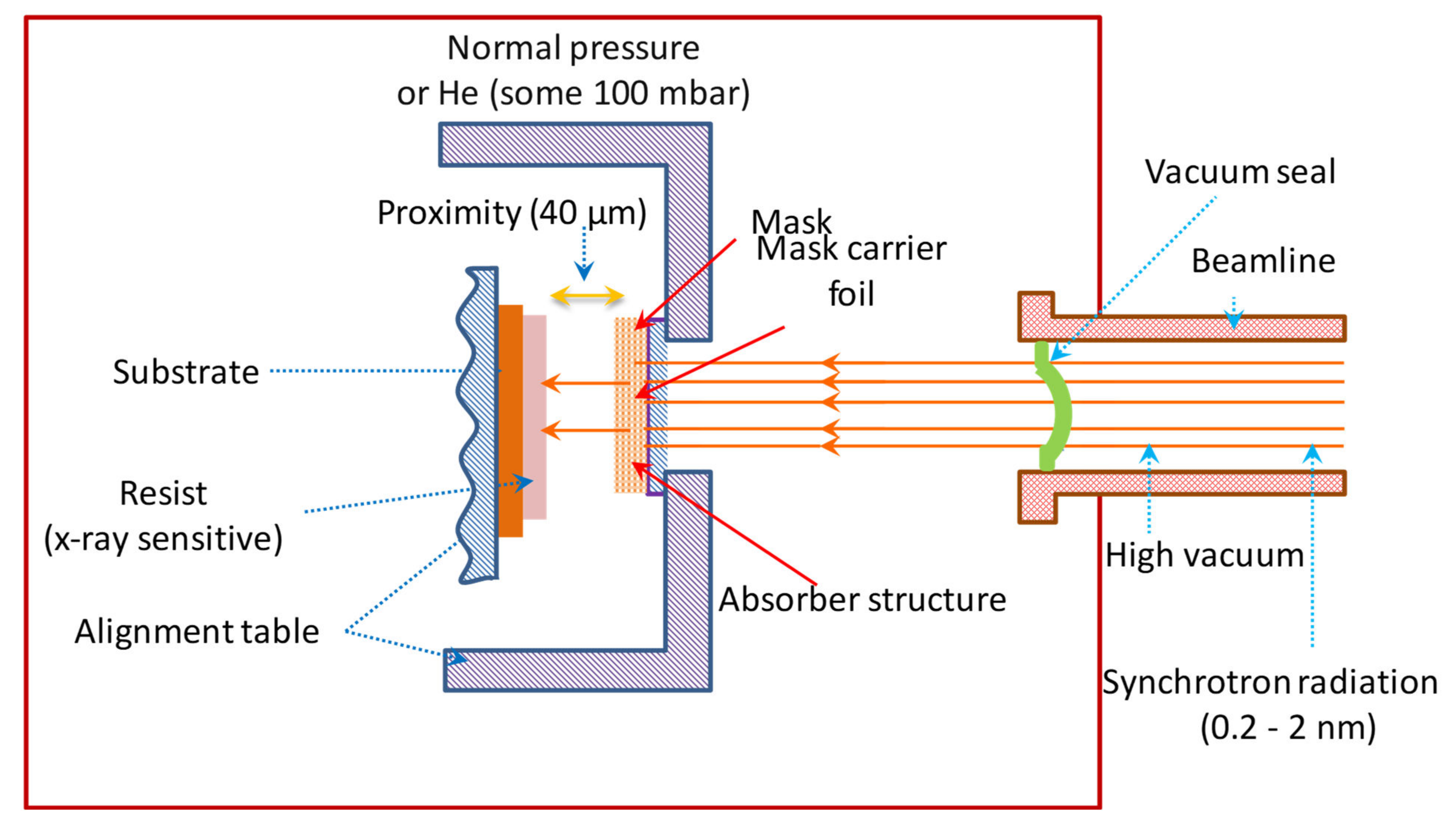
5. X-ray Lithography
5.1. Resists
5.2. Aligners
5.3. Limitations
6. Ion Beam Lithography
6.1. Resist
6.1.1. Organic Resist for FIB
6.1.2. Positive Resist for Proton Beam
6.1.3. Resist for Proton Beam
6.1.4. Resist for IPL
6.2. Mask
6.3. Limitations
7. Conclusions and Future Aspects
Author Contributions
Funding
Institutional Review Board Statement
Informed Consent Statement
Data Availability Statement
Conflicts of Interest
References
- Pease, R.F.; Chou, S.Y. Lithography and Other Patterning Techniques for Future Electronics. Proc. IEEE 2008, 96, 248–270. [Google Scholar] [CrossRef]
- Ko, W.H. Trends and frontiers of MEMS. Sens. Actuators A Phys. 2007, 136, 62–67. [Google Scholar] [CrossRef]
- Peer, D.; Karp, J.M.; Hong, S.; Farokhzad, O.C.; Margalit, R.; Langer, R. Nanocarriers as an emerging platform for cancer therapy. Nat. Nanotechnol. 2007, 2, 751–760. [Google Scholar] [CrossRef] [PubMed]
- Lammers, T.; Hennink, W.E.; Storm, G. Tumour-targeted nanomedicines: Principles and practice. Br. J. Cancer 2008, 99, 392–397. [Google Scholar] [CrossRef]
- Davis, M.E.; Chen, Z.; Shin, D.M. Nanoparticle therapeutics: An emerging treatment modality for cancer. Nat. Rev. Drug Discov. 2008, 7, 771–782. [Google Scholar] [CrossRef]
- Chavan, A.V.; Wise, K.D. Batch-processed vacuum-sealed capacitive pressure sensors. J. Microelectromech. Syst. 2001, 10, 580–588. [Google Scholar] [CrossRef]
- Kabanov, A.V.; Gendelman, H.E. Nanomedicine in the diagnosis and therapy of neurodegenerative disorders. Prog. Polym. Sci. 2007, 32, 1054–1082. [Google Scholar] [CrossRef]
- Modi, G.; Pillay, V.; Choonara, Y.E.; Ndesendo, V.M.K.; du Toit, L.C.; Naidoo, D. Nanotechnological applications for the treatment of neurodegenerative disorders. Prog. Neurobiol. 2009, 88, 272–285. [Google Scholar] [CrossRef]
- Ming, L.; Qiuxia, X.; Yinkui, Z. Electron beam lithography and its application in fabricating nano-device. In Proceedings of the 7th International Conference on Solid-State and Integrated Circuits Technology, Beijing, China, 18–21 October 2004. [Google Scholar] [CrossRef]
- Park, J.; Koh, C.; Goo, D.; Kim, I.; Park, C.; Lee, J.; Park, J.; Yeo, J.; Choi, S.-W.; Park, C. The application of EUV lithography for 40 nm node DRAM device and beyond. Altern. Lithogr. Technol. 2009, 7271, 727114. [Google Scholar] [CrossRef]
- Altissimo, M. E-beam lithography for micro-/nanofabrication. Biomicrofluidics 2010, 4, 026503. [Google Scholar] [CrossRef]
- Watt, F.; Bettiol, A.A.; Van Kan, J.A.; Teo, E.J.; Breese, M.B.H. Ion Beam Lithography and Nanofabrication: A Review. Int. J. Nanosci. 2005, 04, 269–286. [Google Scholar] [CrossRef]
- Ito, H. Advances in Chemical Amplification Resist Systems. Jpn. J. Appl. Phys. 1992, 31, 4273–4282. [Google Scholar] [CrossRef]
- Zhu, J.; Holmes, A.S.; Arnold, J.; Lawes, R.A.; Prewett, P.D. Laminated dry film resist for microengineering applications. Microelectron. Eng. 1996, 30, 365–368. [Google Scholar] [CrossRef]
- Wu, Q.; Lu, Z.G.; Williams, G.; Zach, F.X.; Liegl, B. Optimization of Segmented Alignment Marks for Advanced Semiconductor Fabrication Processes; Sullivan, N.T., Ed.; SPIE: Bellingham, WA, USA, 2001; p. 234. [Google Scholar]
- Zhang, L.; Dong, L.; Su, X.; Wei, Y.; Ye, T. New alignment mark designs in single patterning and self-aligned double patterning. Microelectron. Eng. 2017, 179, 18–24. [Google Scholar] [CrossRef]
- Bijnen, F.G.C.; van Buel, W.; Gui, C.Q.; Lof, J. Front-to-Back Alignment Metrology; Engelstad, R.L., Ed.; SPIE: Bellingham, WA, USA, 2003; p. 641. [Google Scholar]
- Warrick, S.; Hinnen, P.; Van Haren, R.; Smith, C.; Megens, H.; Fu, C.-C. Integration of New Alignment Mark Designs in Dual Inlaid Copper Interconnect Processes. Proc. SPIE 2002, 4691, 971–980. [Google Scholar]
- Zhang, L.; Feng, Y.; Dong, L.; Su, X.; Tian, Z.; Fang, C.; Wei, Y.; Ye, T. New Alignment Mark Design Structures for Higher Diffraction Order Wafer Quality Enhancement. In Proceedings of the Metrology, Inspection, and Process Control for Microlithography XXXI; SPIE: Bellingham, WA, USA, 2017; Volume 10145, p. 101452C. [Google Scholar]
- Ohtsuka, H.; Abe, K.; Onodera, T.; Kuwahara, K.; Taguchi, T. Conjugate Twin-Shifter for the New Phase Shift Method to High Resolution Lithography. Proc. SPIE 1991, 1463, 112–123. [Google Scholar]
- Gates, B.D.; Xu, Q.; Stewart, M.; Ryan, D.; Willson, C.G.; Whitesides, G.M. New Approaches to Nanofabrication: Molding, Printing, and Other Techniques. Chem. Rev. 2005, 105, 1171–1196. [Google Scholar] [CrossRef]
- Sanders, D.P. Advances in Patterning Materials for 193 nm Immersion Lithography. Chem. Rev. 2010, 110, 321–360. [Google Scholar] [CrossRef]
- Tichenor, D.A.; Ray-Chaudhuri’, A.K.; Leer, S.H.; Chapman’, H.N.; Reploglea, W.C.; Bergera, K.W.; Stulena, R.H.; Kubiaka, G.D.; Klebanofr, L.E.; Wronoskyc, J.B.; et al. Initial Results from the EUV Engineering Test Stand. In Proceedings of the International Symposium On Optical Science And Technology, San Diego, CA, USA, 29 July–3 August 2001. [Google Scholar]
- Meiling, H.; Benschop, J.; Dingera, U.; Kürz’, P. Progress of the EUVL alpha tool. In Emerging Lithographic Technologies V; SPIE: Bellingham, WA, USA, 2001. [Google Scholar]
- Sun, Y.; Singh, N. Room-temperature operation of silicon single-electron transistor fabricated using optical lithography. IEEE Trans. Nanotechnol. 2011, 10, 96–98. [Google Scholar] [CrossRef]
- Pavel, E.; Marinescu, V.; Lungulescu, M. Graphene nanopatterning by Quantum Optical Lithography. Optik 2020, 203, 163532. [Google Scholar] [CrossRef]
- Dhawan, A.R.; Nasilowski, M.; Wang, Z.; Dubertret, B.; Maître, A. Fabrication of Efficient Single-Emitter Plasmonic Patch Antennas by Deterministic In Situ Optical Lithography using Spatially Modulated Light. Adv. Mater. 2022, 34, 2108120. [Google Scholar] [CrossRef]
- Okazaki, S. High resolution optical lithography or high throughput electron beam lithography: The technical struggle from the micro to the nano-fabrication evolution. Microelectron. Eng. 2015, 133, 23–35. [Google Scholar] [CrossRef]
- Owa, S.; Nagasaka, H. Immersion Lithography; Its Potential Performance and Issues; Yen, A., Ed.; SPIE: Bellingham, WA, USA, 2003; p. 724. [Google Scholar]
- Otto, O.W.; Garofalo, J.G.; Low, K.K.; Yuan, C.-M.; Henderson, R.C.; Pierrat, C.; Kostelak, R.L.; Vaidya, S.; Vasudev, P.K. Automated Optical Proximity Correction: A Rules-Based Approach; Brunner, T.A., Ed.; SPIE: Bellingham, WA, USA, 1994; pp. 278–293. [Google Scholar]
- Chen, Y.-C.; Kuo, Y.-T.; Ho, T.-H. Photo-polymerization properties of type-II photoinitiator systems based on 2-chlorohexaaryl biimidazole (o-Cl-HABI) and various N -phenylglycine (NPG) derivatives. Photochem. Photobiol. Sci. 2019, 18, 190–197. [Google Scholar] [CrossRef]
- MacDonald, S.A.; Frechet, J.M.J.; Ito, H.; Grant Willson, C. Resist materials. Microelectron. Eng. 1985, 3, 277–278. [Google Scholar] [CrossRef]
- Ito, H. Chemical Amplification Resists: History and Development within IBM. IBM J. Res. Dev. 1997, 41, 119–130. [Google Scholar] [CrossRef]
- Shaw, J.M.; Gelorme, J.D.; LaBianca, N.C.; Conley, W.E.; Holmes, S.J. Negative photoresists for optical lithography. IBM J. Res. Dev. 1997, 41, 81–94. [Google Scholar] [CrossRef]
- Zawadzka, A.; Paszkiewicz, R. Limitations of optical lithography on non-planar surfaces. Mater. Sci. Semicond. Process. 2022, 143, 106548. [Google Scholar] [CrossRef]
- Chopra, J. Analysis of Lithography Based Approaches in Development of Semiconductors. Int. J. Comput. Sci. Inf. Technol. 2014, 6, 61–72. [Google Scholar] [CrossRef]
- Fu, N.; Liu, Y.; Ma, X.; Chen, Z. EUV Lithography: State-of-the-Art Review. J. Microelectron. Manuf. 2019, 2, 1–6. [Google Scholar] [CrossRef]
- Nguyen, K.B. Fabrication of metal–oxide–semiconductor devices with extreme ultraviolet lithography. J. Vac. Sci. Technol. B Microelectron. Nanom. Struct. 1996, 14, 4188. [Google Scholar] [CrossRef]
- Meiling, H.; Benschop, J.; Hartman, R.; Kurza, P.; Hoghoj, P.; Geylc, R.; Harned, N. EXTATIC, ASML’s a-Tool Development for EUVL; SPIE: Bellingham, WA, USA, 2002. [Google Scholar]
- Wagner, C.; Harned, N. EUV lithography: Lithography gets extreme. Nat. Photonics 2010, 4, 24–26. [Google Scholar] [CrossRef]
- Yang, D.; Wang, D.; Huang, Q.; Song, Y.; Wu, J.; Li, W.; Wang, Z.; Tang, X.; Xu, H.; Liu, S.; et al. The development of laser-produced plasma EUV light source. Chip 2022, 100019, in press. [Google Scholar] [CrossRef]
- Tichenor, D.A.; Ray-Chaudhuri, A.K.; Replogle, W.C.; Stulena, R.H.; Kubiaka, G.D.; Rockett, P.D.; Klebanoffa, L.E.; Jeffersona, K.L.; Leunga, A.H.; Wronoskyb, J.B.; et al. System Integration and Performance of the EUV Engineering Test Stand. In Emerging Lithographic Technologies V; SPIE: Bellingham, WA, USA, 2001. [Google Scholar]
- Tichenor, D.A.; Ray-Chaudhuri, A.K.; Lee, S.H.; Chapman, H.N.; Replogle, W.C.; Berger, K.W.; Stulen, R.H.; Kubiak, G.D.; Klebanoff, L.E.; Wronosky, J.B.; et al. Initial Results from the EUV Engineering Test Stand; Tichenor, D.A., Folta, J.A., Eds.; SPIE: Bellingham, WA, USA, 2001; pp. 9–18. [Google Scholar]
- Booth, M.; Brisco, O.; Brunton, A.; Cashmore, J.; Elbourn, P.; Elliner, G.; Gower, M.; Greuters, J.; Grunewald, P.; Gutierrez, R.; et al. High-Resolution EUV Imaging Tools for Resist Exposure and Aerial Image Monitoring. In Proceedings of the Emerging Lithographic Technologies IX; SPIE: Bellingham, WA, USA, 2005; Volume 5751, p. 78. [Google Scholar]
- Oizumi, H.; Tanaka, Y.; Kumasaka, F.; Nishiyama, I.; Kondo, H.; Shiraishi, M.; Oshino, T.; Sugisaki, K.; Murakami, K. Lithographic Performance of High-Numerical-Aperture (NA = 03) EUV Small-Field Exposure Tool (HINA). In Proceedings of the Emerging Lithographic Technologies IX; SPIE: Bellingham, WA, USA, 2005; Volume 5751, p. 102. [Google Scholar]
- Meiling, H.; Benschop, J.P.; Dinger, U.; Kuerz, P. Progress of the EUVL alpha Tool; Dobisz, E.A., Ed.; SPIE: Bellingham, WA, USA, 2001; pp. 38–50. [Google Scholar]
- Chkhalo, N.I.; Polkovnikov, V.N.; Salashchenko, N.N.; Toropov, M.N. Problems and Prospects of Maskless (B)EUV Lithography; Lukichev, V.F., Rudenko, K.V., Eds.; SPIE: Bellingham, WA, USA, 2016; p. 102241O. [Google Scholar]
- Van Schoot, J.; van Setten, E.; Troost, K.; Bornebroek, F.; van Ballegoij, R.; Lok, S.; Stoeldraijer, J.; Finders, J.; Graeupner, P.; Zimmermann, J.; et al. High-NA EUV Lithography Exposure Tool Progress. In Proceedings of the Extreme Ultraviolet (EUV) Lithography X; Felix, N.M., Goldberg, K.A., Eds.; SPIE: Bellingham, WA, USA, 2019; p. 3. [Google Scholar]
- Miura, T.; Murakami, K.; Suzuki, K.; Kohama, Y.; Morita, K.; Hada, K.; Ohkubo, Y. Nikon EUVL Development Progress Update; Lercel, M.J., Ed.; SPIE: Bellingham, WA, USA, 2007; p. 651707. [Google Scholar]
- Cao, H.B.; Yueh, W.; Rice, B.J.; Roberts, J.; Bacuita, T.; Chandhok, M. Sources of Line-Width Roughness for EUV Resists. In Proceedings of the Advances in Resist Technology and Processing XXI; SPIE: Bellingham, WA, USA, 2004; Volume 5376, p. 757. [Google Scholar]
- Dai, J.; Ober, C.K. Novel resists with nontraditional compositions for EUV lithography. In The Advances in Resist Technology and Processing XXI, Proceedings of SPIE–The International Society for Optical Engineering, Santa Clara, CA, USA, 23–24 February 2004; SPIE: Bellingham, WA, USA, 2004; Volume 5376, p. 508. [Google Scholar]
- De Silva, A.; Forman, D.; Ober, C.K. Molecular glass resists for EUV lithography. In The Advances in Resist Technology and Processing XXIII, Proceedings of SPIE–The International Society for Optical Engineering, San Jose, CA, USA, 20–22 February 2006; SPIE: Bellingham, WA, USA, 2006; Volume 6153, p. 615341. [Google Scholar]
- Bespalov, I.; Zhang, Y.; Haitjema, J.; Tromp, R.M.; van der Molen, S.J.; Brouwer, A.M.; Jobst, J.; Castellanos, S. Key Role of Very Low Energy Electrons in Tin-Based Molecular Resists for Extreme Ultraviolet Nanolithography. ACS Appl. Mater. Interfaces 2020, 12, 9881–9889. [Google Scholar] [CrossRef]
- Nagahara, S.; Dinh, C.Q.; Yoshida, K.; Shiraishi, G.; Kondo, Y.; Yoshihara, K.; Nafus, K.; Petersen, J.S.; De Simone, D.; Foubert, P.; et al. EUV Resist Chemical Gradient Enhancement by Uv Flood Exposure for Improvement in Euv Resist Resolution, Process Control, Roughness, Sensitivity and Stochastic Defectivity. In Proceedings of the Advances in Patterning Materials and Processes XXXVII; Gronheid, R., Sanders, D.P., Eds.; SPIE: Bellingham, WA, USA, 2020; p. 9. [Google Scholar]
- Thakur, N.; Tseng, L.-T.; Vockenhuber, M.; Ekinci, Y.; Castellanos, S. Stability studies on a sensitive EUV photoresist based on zinc metal oxoclusters. J. Micro/Nanolithogr. MEMS MOEMS 2019, 18, 043504. [Google Scholar] [CrossRef]
- Castellanos Ortega, S.; Wu, L.; Baljozovic, M.; Portale, G.; Kazazis, D.; Vockenhuber, M.; Ekinci, Y.; Jung, T. Ti, Zr, and Hf-Based Molecular Hybrid Materials as EUV Photoresists. In Proceedings of the Extreme Ultraviolet (EUV) Lithography IX; Felix, N.M., Goldberg, K.A., Eds.; SPIE: Bellingham, WA, USA, 2018; p. 6. [Google Scholar]
- Yamamoto, H.; Vesters, Y.; Jiang, J.; De Simone, D.; Vandenberghe, G.; Kozawa, T. Role of Metal Sensitizers for Sensitivity Improvement in EUV Chemically Amplified Resist. J. Photopolym. Sci. Technol. 2018, 31, 747–751. [Google Scholar] [CrossRef]
- Park, J.; Lee, S.-G.; Vesters, Y.; Severi, J.; Kim, M.; De Simone, D.; Oh, H.-K.; Hur, S.-M. Molecular Modeling of EUV Photoresist Revealing the Effect of Chain Conformation on Line-Edge Roughness Formation. Polymers 2019, 11, 1923. [Google Scholar] [CrossRef]
- Brainard, R.; Kruger, S.; Higgins, C.; Revuru, S.; Gibbons, S.; Freedman, D.; Yueh, W.; Younkin, T. Kinetics, Chemical Modeling and Lithography of Novel Acid Amplifiers for Use in EUV Photoresists. J. Photopolym. Sci. Technol. 2009, 22, 43–50. [Google Scholar] [CrossRef]
- Kudo, H.; Niina, N.; Sato, T.; Oizumi, H.; Itani, T.; Miura, T.; Watanabe, T.; Kinoshita, H. Extreme Ultraviolet (EUV)-Resist Material Based on Noria (Water Wheel-like Macrocycle) Derivatives with Pendant Alkoxyl and Adamantyl Ester Groups. J. Photopolym. Sci. Technol. 2012, 25, 587–592. [Google Scholar] [CrossRef]
- Kulshreshtha, P.K.; Maruyama, K.; Kiani, S.; Dhuey, S.; Perera, P.; Blackwell, J.; Olynick, D.; Ashby, P.D. Sub-20nm Lithography Negative Tone Chemically Amplified Resists Using Cross-Linker Additives. In Proceedings of the Advances in Resist Materials and Processing Technology XXX; SPIE: Bellingham, WA, USA, 2013; Volume 8682, p. 86820N. [Google Scholar]
- Rathore, A.; Pollentier, I.; Singh, H.; Fallica, R.; De Simone, D.; De Gendt, S. Effect of molecular weight on the EUV-printability of main chain scission type polymers. J. Mater. Chem. C 2020, 8, 5958–5966. [Google Scholar] [CrossRef]
- Constancias, C.; Richard, M. Phase-Shift Mask for EUV Lithography; SPIE: Bellingham, WA, USA, 2006; Volume 6151. [Google Scholar]
- Han, S.I.; Wasson, J.R.; Mangat, P.J.; Cobb, J.L.; Lucas, K.; Hector, S.D. Novel Design of Att-Psm Structure for Extreme-Ultraviolet Lithography and Enhancement of Image Contrast During Inspection; SPIE: Bellingham, WA, USA, 2002. [Google Scholar]
- Fontaine, B.L.; Pawloski, A. Demonstration of Phase-Shift Masks for Extreme-Ultraviolet Lithography; SPIE: Bellingham, WA, USA.
- Han, S.; Weisbrod, E.; Xie, Q.; Mangat, P.J.S.; Hector, S.D.; Dauksher, W.J. Design and method of fabricating phase-shift masks for extreme-ultraviolet lithography by partial etching into the EUV multilayer mirror. In Proceedings of the Emerging Lithographic Technologies VII, Santa Clara, CA, USA, 16 June 2003. [Google Scholar] [CrossRef]
- Hector, S.; Mangat, P. Review of progress in extreme ultraviolet lithography masks. J. Vac. Sci. Technol. B Microelectron. Nanom. Struct. 2001, 19, 2612. [Google Scholar] [CrossRef]
- Haga, T.; Takenaka, H.; Fukuda, M. At-wavelength extreme ultraviolet lithography mask inspection using a Mirau interferometric microscope. J. Vac. Sci. Technol. B Microelectron. Nanom. Struct. 2000, 18, 2916. [Google Scholar] [CrossRef]
- Kim, S.-S.; Park, J.; Chalykh, R.; Kang, J.; Lee, S.; Woo, S.-G.; Cho, H.-K.; Semiconductor, J.-T.M.; Center, R. Defect inspection of EUV mask blank using confocal microscopy: Simulation and experiment. In Proceedings of the SPIE 31st International Symposium on Advanced Lithography, San Jose, CA, USA, 19–24 February 2006. [Google Scholar] [CrossRef]
- Urbach, J.-P.; Cavelaars, J.F.W.; Kusunose, H.; Liang, T.; Stivers, A.R. EUV substrate and blank inspection with confocal microscopy. In Proceedings of the Photomask Technology, Monterey, CA, USA, 9–12 September 2003; Kimmel, K.R., Staud, W., Eds.; SPIE: Bellingham, WA, USA, 2003; p. 556. [Google Scholar]
- De Silva, A.; Felix, N.; Sha, J.; Lee, J.-K.; Ober, C.K. Molecular glass resists for next generation lithography. In Proceedings of the SPIE Advanced Lithography, San Jose, CA, USA, 22–27 February 2009; p. 69231L. [Google Scholar]
- Folta, J.A.; Davidson, J.C.; Larson, C.C.; Walton, C.C.; Kearney, P.A. Advances in low-defect multilayers for EUVL mask blanks. In Proceedings of the SPIE’s 27th Annual International Symposium on Microlithography, Santa Clara, CA, USA, 3–8 March 2002. [Google Scholar]
- Ma, A.; Kearney, P.; Krick, D. Progress towards the development of a commercial tool and process for EUVL mask blanks. In Proceedings of the Microlithography, San Jose, CA, USA, 27 February–4 March 2005. [Google Scholar]
- Tejnil, E.; Gullikson, E.M.; Stivers, A.R. Characterization of Defect Detection Sensitivity in Inspection of Mask Substrates and Blanks for Extreme-Ultraviolet Lithography. In Proc. SPIE 5567, 24th Annual BACUS Symposium on Photomask Technology, Monterey, CA, USA, 6 December 2004; Staud, W., Weed, J.T., Eds.; SPIE: Bellingham, WA, USA, 2004; p. 943. [Google Scholar]
- Kleineberg, U.; Lin, J.; Neuhaeusler, U.; Slieh, J.; Heinzmann, U.; Weber, N.; Escher, M.; Merkel, M.; Oelsner, A.; Valsaitsev, D.; et al. Actinic EUVL mask blank defect inspection by EUV photoelectron microscopy. In Proceedings of the SPIE 31st International Symposium on Advanced Lithography, San Jose, CA, USA, 19–24 February 2006. [Google Scholar]
- Green, M.; Lallement, R.; Ramadan, M.; Dunn, D.; Kamberian, H.; Sieg, S.; Ham, Y.; Progler, C. EUVL mask process development and verification using advanced modeling and characterization techniques. In Proceedings of the Extreme Ultraviolet (EUV) Lithography XI; Felix, N.M., Lio, A., Eds.; SPIE: Bellingham, WA, USA, 2020; p. 90. [Google Scholar]
- Makhotkin, I.A.; Wu, M.; Soltwisch, V.; Scholze, F.; Philipsen, V. Refined extreme ultraviolet mask stack model. J. Opt. Soc. Am. A 2021, 38, 498. [Google Scholar] [CrossRef]
- Wu, M.; de Marneffe, J.-F.; Opsomer, K.; Detavernier, C.; Delabie, A.; Naujok, P.; Caner, Ö.; Goodyear, A.; Cooke, M.; Saadeh, Q.; et al. Characterization of Ru4−xTax (x = 1,2,3) alloy as material candidate for EUV low-n mask. Micro Nano Eng. 2021, 12, 100089. [Google Scholar] [CrossRef]
- Wallow, T.; Civay, D.; Wang, S.; Hoefnagels, H.F.; Verspaget, C.; Tanriseven, G.; Fumar-Pici, A.; Hansen, S.; Schefske, J.; Singh, M.; et al. EUV Resist Performance: Current Assessment for sub-22-nm Half-Pitch Patterning on NXE:3300. In Proceedings of the SPIE Advanced Lithography, San Jose, CA, USA, 12–16 February 2012; p. 83221J. [Google Scholar]
- Sebastian, E.M.; Jain, S.K.; Purohit, R.; Dhakad, S.K.; Rana, R.S. Nanolithography and its current advancements. Mater. Today Proc. 2019, 26, 2351–2356. [Google Scholar] [CrossRef]
- Sugihara, T.; Nagai, S.; Kaneko, A. High-aspect nano-groove fabrication in thick film resists using 150-kV high acceleration voltage electron beam lithography. Precis. Eng. 2022, 74, 205–208. [Google Scholar] [CrossRef]
- Servin, I.; Pourteau, M.-L.; Pradelles, J.; Essomba, P.; Lattard, L.; Brandt, P.; Wieland, M. Progress and process improvements for multiple electron-beam direct write. Jpn. J. Appl. Phys. 2017, 56, 06GC03. [Google Scholar] [CrossRef]
- Carr, D.W.; Tiberio, R.C. Direct-write Electron Beam Lithography: History and State of the Art. MRS Proc. 1999, 584, 33. [Google Scholar] [CrossRef]
- De Boer, G.; Dansberg, M.P.; Jager, R.; Peijster, J.J.M.; Slot, E.; Steenbrink, S.W.H.K.; Wieland, M.J. MAPPER: Progress toward a High-Volume Manufacturing System. In Proc. SPIE 8680, Alternative Lithographic Technologies V, San Jose, CA, USA, 26 March 2013; Tong, W.M., Resnick, D.J., Eds.; SPIE: Bellingham, WA, USA, 2013; p. 86800O. [Google Scholar]
- Hasan, R.M.M.; Luo, X. Promising Lithography Techniques for Next-Generation Logic Devices. Nanomanuf. Metrol. 2018, 1, 67–81. [Google Scholar] [CrossRef]
- Liu, E.D.; Prescop, T. Optimization of e-beam landing energy for EBDW. In Proceedings of the SPIE Advanced Lithography, San Jose, CA, USA, 27 February–3 March 2011; Herr, D.J.C., Ed.; SPIE: Bellingham, WA, USA, 2011; Volume 8680, p. 79701S. [Google Scholar]
- Esashi, M.; Miyaguchi, H.; Kojima, A.; Ikegami, N.; Koshida, N.; Ohyi, H. Development of a massively parallel electron beam write (MPEBW) system: Aiming for the digital fabrication of integrated circuits. Jpn. J. Appl. Phys. 2022, 61, SD0807. [Google Scholar] [CrossRef]
- Esashi, M.; Kojima, A.; Ikegami, N.; Miyaguchi, H.; Koshida, N. Development of massively parallel electron beam direct write lithography using active-matrix nanocrystalline-silicon electron emitter arrays. Microsyst. Nanoeng. 2015, 1, 15029. [Google Scholar] [CrossRef]
- Hasan, M.N.; Lee, S.-Y.; Ahn, B.-S.; Choi, J.; Kim, S.-B.; Jeon, C.-U. Effects of abnormal beams on writing qualities in massively-parallel e-beam systems. J. Vac. Sci. Technol. B 2019, 37, 061609. [Google Scholar] [CrossRef]
- Fernández-Pacheco, A.; Skoric, L.; De Teresa, J.M.; Pablo-Navarro, J.; Huth, M.; Dobrovolskiy, O.V. Writing 3D nanomagnets using focused electron beams. Materials 2020, 13, 3774. [Google Scholar] [CrossRef]
- Fischer, P.; Sanz-Hernández, D.; Streubel, R.; Fernández-Pacheco, A. Launching a new dimension with 3D magnetic nanostructures. APL Mater. 2020, 8, 010701. [Google Scholar] [CrossRef]
- Fernández-Pacheco, A.; Streubel, R.; Fruchart, O.; Hertel, R.; Fischer, P.; Cowburn, R.P. Three-dimensional nanomagnetism. Nat. Commun. 2017, 8, 15756. [Google Scholar] [CrossRef]
- Hunt, M.; Taverne, M.; Askey, J.; May, A.; Van Den Berg, A.; Ho, Y.L.D.; Rarity, J.; Ladak, S. Harnessing multi-photon absorption to produce three-dimensional magnetic structures at the nanoscale. Materials 2020, 13, 761. [Google Scholar] [CrossRef]
- Winkler, R.; Fowlkes, J.D.; Rack, P.D.; Plank, H. 3D nanoprinting via focused electron beams. J. Appl. Phys. 2019, 125, 210901. [Google Scholar] [CrossRef]
- Hong, Y.; Zhao, D.; Liu, D.; Ma, B.; Yao, G.; Li, Q.; Han, A.; Qiu, M. Three-Dimensional in Situ Electron-Beam Lithography Using Water Ice. Nano Lett. 2018, 18, 5036–5041. [Google Scholar] [CrossRef]
- Tiddi, W.; Elsukova, A.; Beleggia, M.; Han, A. Organic ice resists for 3D electron-beam processing: Instrumentation and operation. Microelectron. Eng. 2018, 192, 38–43. [Google Scholar] [CrossRef]
- Lee, B.; Hong, J.; Amos, N.; Dumer, I.; Litvinov, D.; Khizroev, S. Sub-10-nm-resolution electron-beam lithography toward very-high-density multilevel 3D nano-magnetic information devices. J. Nanopart. Res. 2013, 15, 1665. [Google Scholar] [CrossRef]
- Wu, B.; Kumar, A. Extreme ultraviolet lithography: A review. J. Vac. Sci. Technol. B Microelectron. Nanom. Struct. 2007, 25, 1743. [Google Scholar] [CrossRef]
- Aktary, M.; Jensen, M.O.; Westra, K.L.; Brett, M.J.; Freeman, M.R. High-resolution pattern generation using the epoxy novolak SU-8 2000 resist by electron beam lithography. J. Vac. Sci. Technol. B Microelectron. Nanom. Struct. 2003, 21, L5–L7. [Google Scholar] [CrossRef]
- Yoo, J.B.; Park, S.W.; Kang, H.N.; Mondkar, H.S.; Sohn, K.; Kim, H.M.; Kim, K.B.; Lee, H. Triphenylsulfonium salt methacrylate bound polymer resist for electron beam lithography. Polymer 2014, 55, 3599–3604. [Google Scholar] [CrossRef]
- Reichmanis, E.; Hanson, J.E.; Kanga, R.S.; Heimbrook, L.A.; Emerson, A.B.; Baiocchi, F.A.; Vaidya, S.A. Effect of Post-Exposure Delay in Positive Acting Chemically Amplified Resists: An Analytical Study. Polym. Eng. Sci. 1992, 32, 1565–1570. [Google Scholar]
- Krysak, M.; Jung, B.; Thompson, M.O.; Ober, C.K. Investigation of acid diffusion during laser spike annealing with systematically designed photoacid generators. In Proceedings of the SPIE 8325, Advances in Resist Materials and Processing Technology XXIX, San Jose, CA, USA, 12 February 2012; Somervell, M.H., Wallow, T.I., Eds.; SPIE: Bellingham, WA, USA, 2012; p. 83250M. [Google Scholar] [CrossRef]
- Singh, V.; Satyanarayana, V.S.V.; Sharma, S.K.; Ghosh, S.; Gonsalves, K.E. Towards novel non-chemically amplified (n-CARS) negative resists for electron beam lithography applications. J. Mater. Chem. C 2014, 2, 2118. [Google Scholar] [CrossRef]
- Tada, T.; Kanayama, T. Nanolithography Using Fullerene Films as an Electron Beam Resist. Jpn. J. Appl. Phys. 1996, 35, L63–L65. [Google Scholar] [CrossRef]
- Hobbs, R.G.; Petkov, N.; Holmes, J.D. Semiconductor Nanowire Fabrication by Bottom-Up and Top-Down Paradigms. Chem. Mater. 2012, 24, 1975–1991. [Google Scholar] [CrossRef]
- Stowers, J.; Keszler, D.A. High resolution, high sensitivity inorganic resists. Microelectron. Eng. 2009, 86, 730–733. [Google Scholar] [CrossRef]
- Mohammad, M.A.; Koshelev, K.; Fito, T.; Zheng, D.A.Z.; Stepanova, M.; Dew, S. Study of development processes for ZEP-520 as a high-resolution positive and negative tone electron beam lithography resist. Jpn. J. Appl. Phys. 2012, 51, 06FC05. [Google Scholar] [CrossRef]
- Abbas, A.S.; Alqarni, S.; Shokouhi, B.B.; Yavuz, M.; Cui, B. Water soluble and metal-containing electron beam resist poly(sodium 4-styrenesulfonate). Mater. Res. Express 2015, 1, 045102. [Google Scholar] [CrossRef]
- Kofler, J.; Schmoltner, K.; Klug, A.; List-Kratochvil, E.J.W. Highly robust electron beam lithography lift-off process using chemically amplified positive tone resist and PEDOT:PSS as a protective coating. J. Micromech. Microeng. 2014, 24, 095010. [Google Scholar] [CrossRef]
- Canalejas-Tejero, V.; Carrasco, S.; Navarro-Villoslada, F.; García Fierro, J.L.; Capel-Sánchez, M.d.C.; Moreno-Bondi, M.C.; Barrios, C.A. Ultrasensitive non-chemically amplified low-contrast negative electron beam lithography resist with dual-tone behaviour. J. Mater. Chem. C 2013, 1, 1392. [Google Scholar] [CrossRef]
- Okamura, H.; Forman, D.C.; Ober, C.K. C60-containing polymers for electron beam lithography. Polym. Bull. 2014, 71, 2395–2405. [Google Scholar] [CrossRef]
- Grant, D.J.; Grant, D.J. Electron-Beam Lithography: From Past to Present; University of Waterloo: Waterloo, ON, Canada, 2003. [Google Scholar]
- Randall, J.N.; Owen, J.H.G.; Lake, J.; Fuchs, E. Next generation of extreme-resolution electron beam lithography. J. Vac. Sci. Technol. B 2019, 37, 061605. [Google Scholar] [CrossRef]
- Shukla, R.; Kannojia, H.K.; Mukherjee, C.; Sankar, P.R.; Thakur, B.S.; Sinha, A.K.; Pandey, D. Challenges in fabrication of high aspect ratio electrostatic comb-drive microactuator using one-step X-ray lithography. ISSS J. Micro. Smart Syst. 2020, 9, 173–180. [Google Scholar] [CrossRef]
- Meyer, P.; Beckenbach, T.; An, F.; Schröter, T.; Schulz, J.; Mohr, J. X-ray gratings for grating-based x-ray DPCI fabricated using the deep x-ray lithography process: State of the art. In Proceedings of the XNPIG Conference, Zurich, Switzerland, 12–15 September 2017. [Google Scholar] [CrossRef]
- Ruiz-Yaniz, M.; Koch, F.; Zanette, I.; Rack, A.; Meyer, P.; Kunka, D.; Hipp, A.; Mohr, J.; Pfeiffer, F. X-ray grating interferometry at photon energies over 180 keV. Appl. Phys. Lett. 2015, 106, 151105. [Google Scholar] [CrossRef]
- Notohamiprodjo, S.; Treitl, K.M.; Hauke, C.; Sutter, S.M.; Auweter, S.; Pfeiffer, F.; Reiser, M.F.; Hellbach, K. Imaging characteristics of intravascular spherical contrast agents for grating-based x-ray dark-field imaging—Effects of concentrations, spherical sizes and applied voltage. Sci. Rep. 2020, 10, 9405. [Google Scholar] [CrossRef]
- Deng, X.; Dai, G.; Liu, J.; Hu, X.; Bergmann, D.; Zhao, J.; Tai, R.; Cai, X.; Li, Y.; Li, T.; et al. A new type of nanoscale reference grating manufactured by combined laser-focused atomic deposition and x-ray interference lithography and its use for calibrating a scanning electron microscope. Ultramicroscopy 2021, 226, 113293. [Google Scholar] [CrossRef]
- Smith, H.I.; Spears, D.L.; Bernacki, S.E. X-ray Lithography: A Complementary Technique to Electron Beam Lithography. J. Vac. Sci. Technol. 1973, 10, 913–917. [Google Scholar] [CrossRef]
- Maldonado, J.R.; Poulsen, M.E.; Saunders, T.E.; Vratny, F.; Zacharias, A. X-ray Lithography Source Using a Stationary Solid Pd Target. J. Vac. Sci. Technol. 1979, 16, 1942–1945. [Google Scholar] [CrossRef]
- Silverman, J.P. Challenges and progress in X-ray lithography. J. Vac. Sci. Technol. B Microelectron. Nanom. Struct. 1998, 16, 3137. [Google Scholar] [CrossRef]
- Silverman, J.P.; Archie, C.N.; Andrews, D.E.; Weger, A.J. Operating Experience with the Helios Compact Storage Ring at IBM. Nucl. Instrum. Methods Phys. Res. Sect. A Accel. Spectrometers Detect. Assoc. Equip. 1994, 347, 31–38. [Google Scholar] [CrossRef]
- Nazmov, V.P.; Goldenberg, B.G.; Reznikova, E.F.; Boerner, M. lithography Self-Aligned Single-Exposure Deep X-ray Lithography. AIP Conf. Proc. 2020, 2299, 060010. [Google Scholar]
- Maldonado, J.R. X-ray lithography, where it is now, and where it is going. J. Electron. Mater. 1990, 19, 699–709. [Google Scholar] [CrossRef]
- Merkle, K. High-resolution electron microscopy of grain boundaries. Interface Sci. 1995, 2, 311–345. [Google Scholar] [CrossRef]
- Feder, R.; Spiller, E.; Topalian, J. X-Ray Lithography. Polym. Eng. Sci. 1977, 17, 385–389. [Google Scholar] [CrossRef]
- Heuberger, A. X-ray lithography. Microelectron. Eng. 1986, 5, 3–38. [Google Scholar] [CrossRef]
- Aristov, V.V.; Bashkina, G.A.; Erko, A.I. Holography of microobjects in soft X-rays. Opt. Commun. 1980, 34, 332–336. [Google Scholar] [CrossRef]
- Warlaumont, J. X-ray lithography: On the path to manufacturing. J. Vac. Sci. Technol. B Microelectron. Nanom. Struct. 1989, 7, 1634. [Google Scholar] [CrossRef]
- Bock, H.; Dammel, R. Gas-phase reactions. 66. Gas-phase pyrolyses of alkyl azides: Experimental evidence for chemical activation. J. Am. Chem. Soc. 1988, 110, 5261–5269. [Google Scholar] [CrossRef]
- Silverman, J.P. X-ray lithography: Status, challenges, and outlook for 0.13 μm. J. Vac. Sci. Technol. B Microelectron. Nanom. Struct. 1997, 15, 2117. [Google Scholar] [CrossRef]
- Ladd, W.A.; Hess, W.M.; Ladd, M.W. High-Resolution Microradiography. Science 1956, 123, 370–371. [Google Scholar] [CrossRef]
- Haller, I.; Hatzakis, M.; Srinivasan, R. High-resolution Positive Resists for Electron-beam Exposure. IBM J. Res. Dev. 1968, 12, 251–256. [Google Scholar] [CrossRef]
- Haller, I.; Feder, R.; Hatzakis, M.; Spiller, E. Copolymers of Methyl Methacrylate and Methacrylic Acid and Their Metal Salts as Radiation Sensitive Resists. J. Electrochem. Soc. 1979, 126, 154. [Google Scholar] [CrossRef]
- Lenzo, P.V.; Spencer, E.G. High-speed low-power x-ray lithography. Appl. Phys. Lett. 1974, 24, 289–291. [Google Scholar] [CrossRef]
- Wang, N.; Jiang, W.; Zhang, Y. Moiré-based sub-nano misalignment sensing via deep learning for lithography. Opt. Lasers Eng. 2021, 143, 106620. [Google Scholar] [CrossRef]
- Kouno, E. An X-ray stepper for synchrotron radiation lithography. J. Vac. Sci. Technol. B Microelectron. Nanom. Struct. 1988, 6, 2135. [Google Scholar] [CrossRef]
- Ishihara, S. A vertical stepper for synchrotron X-ray lithography. J. Vac. Sci. Technol. B Microelectron. Nanom. Struct. 1989, 7, 1652. [Google Scholar] [CrossRef]
- Leontowich, A.F.G.; Hitchcock, A.P.; Watts, B.; Raabe, J. Sub-25 nm direct write (maskless) X-ray nanolithography. Microelectron. Eng. 2013, 108, 5–7. [Google Scholar] [CrossRef]
- Mojarad, N.; Gobrecht, J.; Ekinci, Y. Interference lithography at EUV and soft X-ray wavelengths: Principles, methods, and applications. Microelectron. Eng. 2015, 143, 55–63. [Google Scholar] [CrossRef]
- Slayman, C.; Bartelt, J.; Mckenna, C. Masked Ion Beam Lithography For Submicrometer Device Fabrication. In Proc. SPIE 0333, Submicron Lithography I Santa Clara, CA, USA, 30 June 1982; SPIE: Bellingham, WA, USA, 1982; pp. 168–176. [Google Scholar]
- Suzuki, K. N channel metal–oxide–semiconductor field-effect transistor with 0.15 μm gate delineated by focused ion beam lithography. J. Vac. Sci. Technol. B Microelectron. Nanom. Struct. 1997, 15, 2342. [Google Scholar] [CrossRef]
- Stanishevsky, A. Patterning of diamond and amorphous carbon films using focused ion beams. Thin Solid Films 2001, 398, 560–565. [Google Scholar] [CrossRef]
- Stanishevsky, A. Focused ion beam patterning of diamondlike carbon films. Diam. Relat. Mater. 1999, 8, 1246–1250. [Google Scholar] [CrossRef]
- Narro, J.; Diaz, R. A New Tool for Automation of Focused Ion Beam Bitmap Milling of Two-and Three-Dimensional Micro and Nanostructures. Microsc. Microanal. 2022, 28, 88–90. [Google Scholar] [CrossRef]
- Van Kan, J.A.; Bettiol, A.A.; Watt, F. Three-dimensional nanolithography using proton beam writing. Appl. Phys. Lett. 2003, 83, 1629–1631. [Google Scholar] [CrossRef]
- Nady, E.; Nagy, G.; Huszánk, R. Functionalization of microfluidic devices by microstructures created with proton beam lithography. Vacuum 2021, 190, 110295. [Google Scholar] [CrossRef]
- Ballof, J.; Ramos, J.P.; Molander, A.; Johnston, K.; Rothe, S.; Stora, T.; Düllmann, C.E. The upgraded ISOLDE yield database—A new tool to predict beam intensities. Nucl. Instrum. Methods Phys. Res. Sect. B Beam Interact. Mater. Atoms 2020, 463, 211–215. [Google Scholar] [CrossRef]
- Whitlow, H.J.; Ng, M.L.; Auzelyte, V.; Maximov, I.; Montelius, L.; Van Kan, J.A.; Bettiol, A.A.; Watt, F. Lithography of high spatial density biosensor structures with sub-100 nm spacing by MeV proton beam writing with minimal proximity effect. Nanotechnology 2004, 15, 223–226. [Google Scholar] [CrossRef]
- Hirscher, S.; Kümmel, M.; Kirch, O.; Domke, W.-D.; Wolter, A.; Käsmaier, R.; Buschbeck, H.; Cekan, E.; Chalupka, A.; Chylik, A.; et al. Ion projection lithography below 70 nm: Tool performance and resist process. Microelectron. Eng. 2002, 61, 301–307. [Google Scholar] [CrossRef]
- Shi, X.; Prewett, P.; Huq, E.; Bagnall, D.; Boden, S. A quantitative comparison between helium ion and electron beam lithography on PMMA resist. In Proceedings of the 42nd International Conference on Micro and Nano Engineering, Vienna, Austria, 19–23 September 2016. [Google Scholar]
- Boden, S.; Shi, X.S. SPIE Newsroom. Helium Ion Beam Lithography for Sub-10nm Pattern Definition; SPIE: Bellingham, WA, USA, 2017. [Google Scholar] [CrossRef]
- Cattoni, A.; Mailly, D.; Dalstein, O.; Faustini, M.; Seniutinas, G.; Rösner, B.; David, C. Sub-10 nm electron and helium ion beam lithography using a recently developed alumina resist. Microelectron. Eng. 2018, 193, 18–22. [Google Scholar] [CrossRef]
- Sidorkin, V.; van Veldhoven, E.; van der Drift, E.; Alkemade, P.; Salemink, H.; Maas, D. Sub-10-nm nanolithography with a scanning helium beam. J. Vac. Sci. Technol. B Microelectron. Nanom. Struct. 2009, 27, L18. [Google Scholar] [CrossRef]
- Luo, F.; Manichev, V.; Li, M.; Mitchson, G.; Yakshinskiy, B.; Gustafsson, T.; Johnson, D.; Garfunkel, E. Helium ion beam lithography (HIBL) using HafSOx as the resist. In Proceedings of the SPIE Advanced Lithography, San Jose, CA, USA, 21–25 February 2016. [Google Scholar] [CrossRef]
- Uchiya, N.; Furuta, Y.; Nishikawa, H.; Watanabe, T.; Haga, J.; Satoh, T.; Oikawa, M.; Ishii, Y.; Kamiya, T. Ni electroplating on a resist micro-machined by proton beam writing. Microsyst. Technol. 2008, 14, 1537–1540. [Google Scholar] [CrossRef]
- Menzel, F.; Spemann, D.; Petriconi, S. Proton beam writing of submicrometer structures at LIPSION. Nucl. Instrum. Methods Phys. Res. Sect. B: Beam Interact. Mater. At. 2007, 260, 419–425. [Google Scholar] [CrossRef]
- Andrea, T.; Rothermel, M.; Reinert, T.; Koal, T.; Butz, T. Creation of 3D microsculptures in PMMA by multiple angle proton irradiation. Nucl. Instrum. Methods Phys. Res. Sect. B Beam Interact. Mater. At. 2011, 269, 2431–2434. [Google Scholar] [CrossRef]
- Sakai, T.; Yasuda, R.; Iikura, H.; Nojima, T.; Koka, M.; Satoh, T.; Ishii, Y.; Oshima, A. Fabrication of fine imaging devices using an external proton microbeam. Nucl. Instrum. Methods Phys. Res. Sect. B Beam Interact. Mater. At. 2014, 332, 238–241. [Google Scholar] [CrossRef]
- Larisch, W.; Koal, T.; Werner, R.; Hohlweg, M.; Reinert, T.; Butz, T. Proton beam writing of microstructures in Agar gel for patterned cell growth. Nucl. Instrum. Methods Phys. Res. Sect. B Beam Interact. Mater. At. 2011, 269, 2444–2447. [Google Scholar] [CrossRef]
- Furuta, Y.; Nishikawa, H.; Satoh, T.; Ishii, Y.; Kamiya, T.; Nakao, R.; Uchida, S. Fabrication and evaluation of 3D-electric micro filters using proton beam writing. Microelectron. Eng. 2009, 86, 1396–1400. [Google Scholar] [CrossRef]
- Menzel, F.; Spemann, D.; Koal, T.; Butz, T. 3D-structures with arbitrary shapes created in negative resists by grayscale proton beam writing. Nucl. Instrum. Methods Phys. Res. Sect. B Beam Interact. Mater. At. 2011, 269, 2427–2430. [Google Scholar] [CrossRef]
- Van Delft, F.; van de Laar, R.; Verschuuren, M.; Platzgummer, E.; Loeschner, H. Template masters for substrate conformal imprint lithography generated by charged particle nanopatterning techniques. In Proceedings of the 26th European Mask and Lithography Conference, Grenoble, France, 18–20 January 2010; p. 75450S. [Google Scholar]
- Chatzichristidi, M.; Rajta, I.; Speliotis, T.; Valamontes, E.; Goustouridis, D.; Argitis, P.; Raptis, I. Aqueous base developable: Easy stripping, high aspect ratio negative photoresist for optical and proton beam lithography. Springer 2008, 14, 1423–1428. [Google Scholar] [CrossRef]
- Valamontes, E.; Chatzichristidi, M.; Tsikrikas, N.; Goustouridis, D.; Raptis, I.; Potiriadis, C.; Van Kan, J.A.; Watt, F. Realization and simulation of high-aspect-ratio micro/nanostructures by proton beam writing. Jpn. J. Appl. Phys. 2008, 47, 8600–8605. [Google Scholar] [CrossRef]
- Wang, Y.H.; Malar, P.; van Kan, J.A. Resist evaluation for proton beam writing, Ni mold fabrication and nano-replication. Microsyst. Technol. 2014, 20, 2079–2088. [Google Scholar] [CrossRef]
- Sano, R.; Hayakawa, S.; Hayashi, H.; Ishii, Y.; Nishikawa, H. Micro-structuring of epoxy resists containing nanoparticles by proton beam writing. Nucl. Instrum. Methods Phys. Res. Sect. B Beam Interact. Mater. At. 2017, 404, 228–232. [Google Scholar] [CrossRef]
- Kubena, R.L. Sub-20-nm-wide line fabrication in poly(methylmethacrylate) using a Ga+ microprobe. J. Vac. Sci. Technol. B Microelectron. Nanom. Struct. 1989, 7, 1798. [Google Scholar] [CrossRef]
- Tseng, A.A. Recent developments in micromilling using focused ion beam technology. J. Micromech. Microeng. 2004, 14, 15–34. [Google Scholar] [CrossRef]
- Butschke, J.; Ehrmann, A.; Haugeneder, E.; Irmscher, M.; Kaesmaier, R.; Kragler, K.; Letzkus, F.; Loeschner, H.; Mathuni, J.; Rangelow, I.W.; et al. PN and SOI wafer flow process for stencil mask fabrication. In Proceedings of the 15th European Conference on Mask Technology for Integrated Circuits and Micro-Components, Munich, Germany, 16–17 November 1998; p. 20. [Google Scholar]


| Tool Name | Developer | Year | EUV Source | NA | Reduction | Mirrors | Field Size (mm2) | Resolution (nm) | Ref. |
|---|---|---|---|---|---|---|---|---|---|
| ETS | EUV LLC | 2001 | LPP | 0.1 | 4× | 4 | 24 × 32.5 | 100 | [42] |
| MS-13 | EXITECH | 2004 | Xenon DPP | 0.3 | 5× | 0.6 × 0.2 | 32 | [44] | |
| HINA-3 | NIKON | 2005 | 0.3 | 0.3 × 0.5 | 30 | [45] | |||
| AD Steppers | ASML | 2006 | Tin DPP | 0.25 | 4× | 6 | 26 × 33 | 50 | [24] |
| EUV1 | NIKON | 2007 | Xenon DPP | 0.3 | 5× | 6 | 25 | [49] | |
| NXE3100 | ASML | 2010 | 0.25 | 28 | [47] | ||||
| NXE3300B | ASML | 2013 | 0.33 | 13 nm for single exposure and 9 nm for double exposure | [47] |
| Parameters | Resolution | LWR | Sensitivity |
|---|---|---|---|
| Dimensions | <10 nm | <15% | <20 mJ/cm2 |
| Resist | Post Bake Exposure Temp. (°C) | Time of Developing (s) | Developing Solution | Contrast | Sensitivity (µC/cm2) | Resolution (nm) | Ref. |
|---|---|---|---|---|---|---|---|
| GMA-co-MMA-co-TPSMA | dimethylformamide | 300 | 15 | [100] | |||
| GMA-co-MMA-co-TPSMA | 80 | 120 | dimethylformamide | 70 | 20 | [100] | |
| 40XT | 5 | PEDOT:PSS (No dilution) | 8 ± 2 | 8 | 95 | [109] | |
| 40XT | 120 | PEDOT:PSS (40% dilution) | 10 ± 0.3 | 7.5 | 80 | [109] | |
| MAPDST-MMA | 100 | 120 | TMAH | 1.8 | 2.06 | 20 | [103] |
| (P(HEMA-co-MAAEMA)) | methanol | 1.2 | 0.89 | 125 | [110] | ||
| C60−(P(CMSx−HS))2 | acetone | 40 | 50 | [111] | |||
| (P(HEMA-co-MAAEMA)) | amyl acetate | 4.77 | 172 | 10 | [110] | ||
| HafSOx | TMAH | 2.5 | 21 | 7 | [106] | ||
| ZircSOx | TMAH | 2.6 | 7.6 | 7 | [106] |
| Resist Name | Nature | Required Incident Dose (J cm−2) | Resolution | Ref. |
|---|---|---|---|---|
| PMMA | Positive | 0.33 | 350 Å | [132] |
| PMMA | Positive | 0.5 | 50 Å | [133] |
| TIP(MMA-MMA) | Positive | 0.024 | 1000 Å | [132] |
| CoP (MMA-MAA) | Positive | 0.05 | 500 Å | [134] |
| DCIPA | Negative | 0.0078 | 0.5 µm | [132] |
| Epoxidized polybutadiene | Negative | 0.0015 | 1 µm | [135] |
| Resist | Type of Resist | Fluence (ions/cm2) | Energy of Proton | Aspect Ratio | Smallest Feature Written | Ref. |
|---|---|---|---|---|---|---|
| PMMA | Positive | 5.0–9.4 × 10¹³ | 2 | 100 | 20–30 nm | [156] |
| SU-8 | Negative | 1.9 × 10¹³ | 1 | 166 | 60 nm | [146] |
| HSQ | Negative | 1.9–13 × 1013 | 2 | 40 | 19 nm | [163] |
| TADEP | Negative | 1.6–15 × 1013 | 2 | 18 | 110 nm | [165] |
| AGAR | Positive | 3.0 × 10¹⁴ | 2.25 | 0.3 | 15 µm | [160] |
| Forturan | Positive | 6.3 × 10¹¹ | 2 | 13.3 | 3 µm | [166] |
| PDMS | Negative | 0.13–40 × 1013 | 1 | 1.3 | 10 µm | [167] |
| ma-N 2401 | Negative | 2.5 × 10¹³ | 1 | 1.6 | 60 nm | [166] |
Publisher’s Note: MDPI stays neutral with regard to jurisdictional claims in published maps and institutional affiliations. |
© 2022 by the authors. Licensee MDPI, Basel, Switzerland. This article is an open access article distributed under the terms and conditions of the Creative Commons Attribution (CC BY) license (https://creativecommons.org/licenses/by/4.0/).
Share and Cite
Sharma, E.; Rathi, R.; Misharwal, J.; Sinhmar, B.; Kumari, S.; Dalal, J.; Kumar, A. Evolution in Lithography Techniques: Microlithography to Nanolithography. Nanomaterials 2022, 12, 2754. https://doi.org/10.3390/nano12162754
Sharma E, Rathi R, Misharwal J, Sinhmar B, Kumari S, Dalal J, Kumar A. Evolution in Lithography Techniques: Microlithography to Nanolithography. Nanomaterials. 2022; 12(16):2754. https://doi.org/10.3390/nano12162754
Chicago/Turabian StyleSharma, Ekta, Reena Rathi, Jaya Misharwal, Bhavya Sinhmar, Suman Kumari, Jasvir Dalal, and Anand Kumar. 2022. "Evolution in Lithography Techniques: Microlithography to Nanolithography" Nanomaterials 12, no. 16: 2754. https://doi.org/10.3390/nano12162754