
Gallium Oxide Nanostructures: A Review of Synthesis, Properties and Applications


Abstract
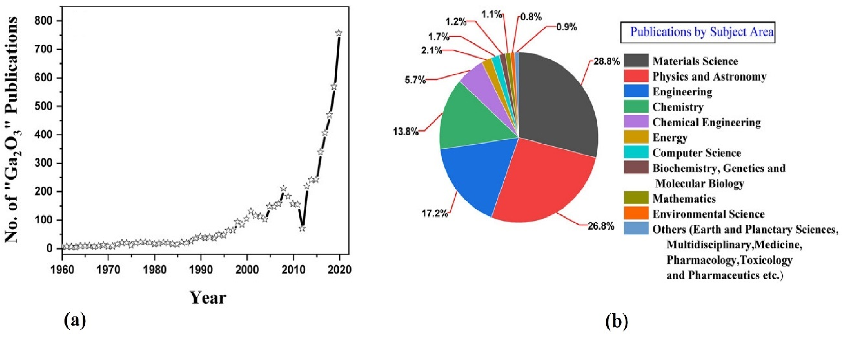
:1. Introduction
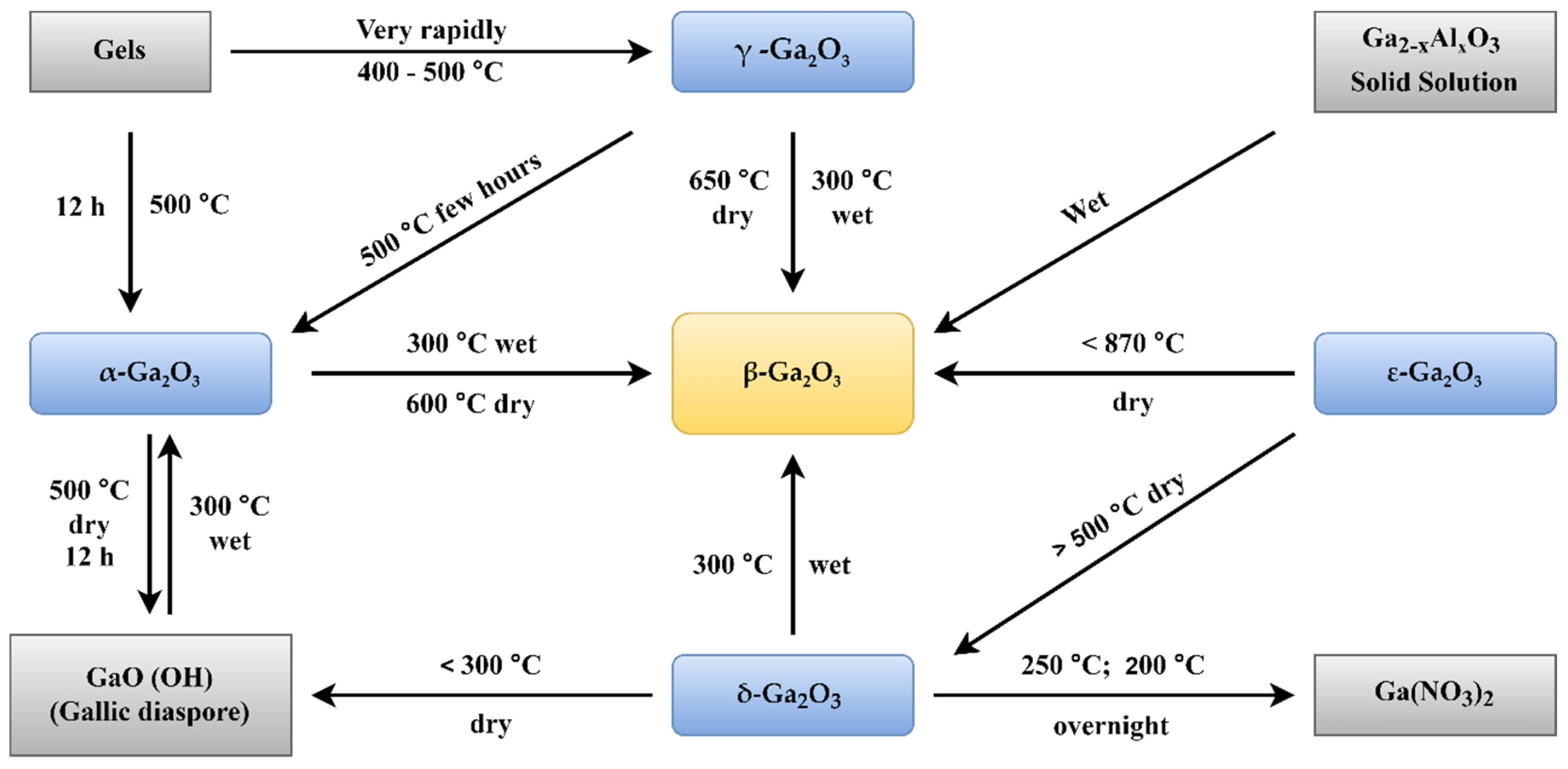
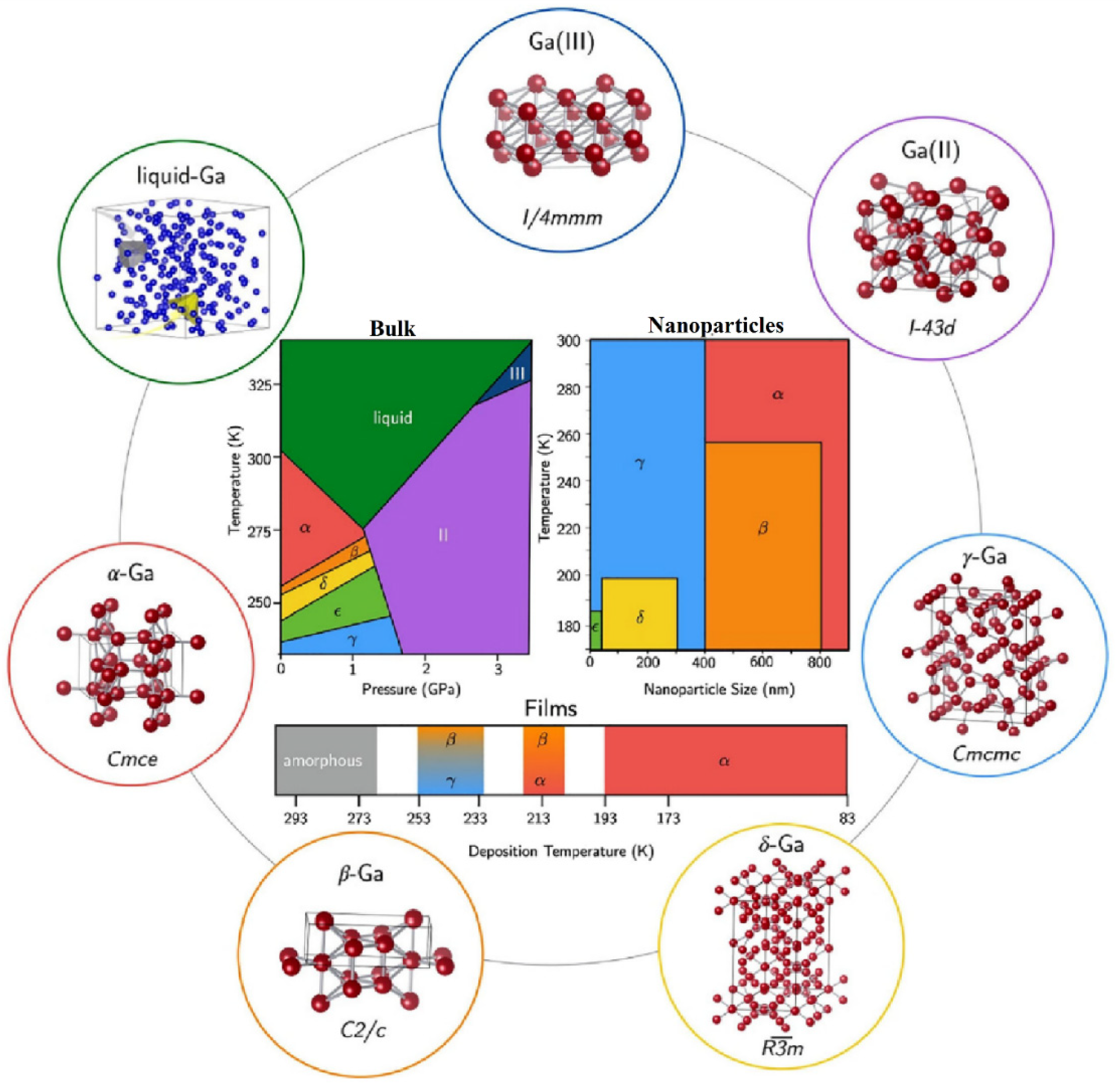
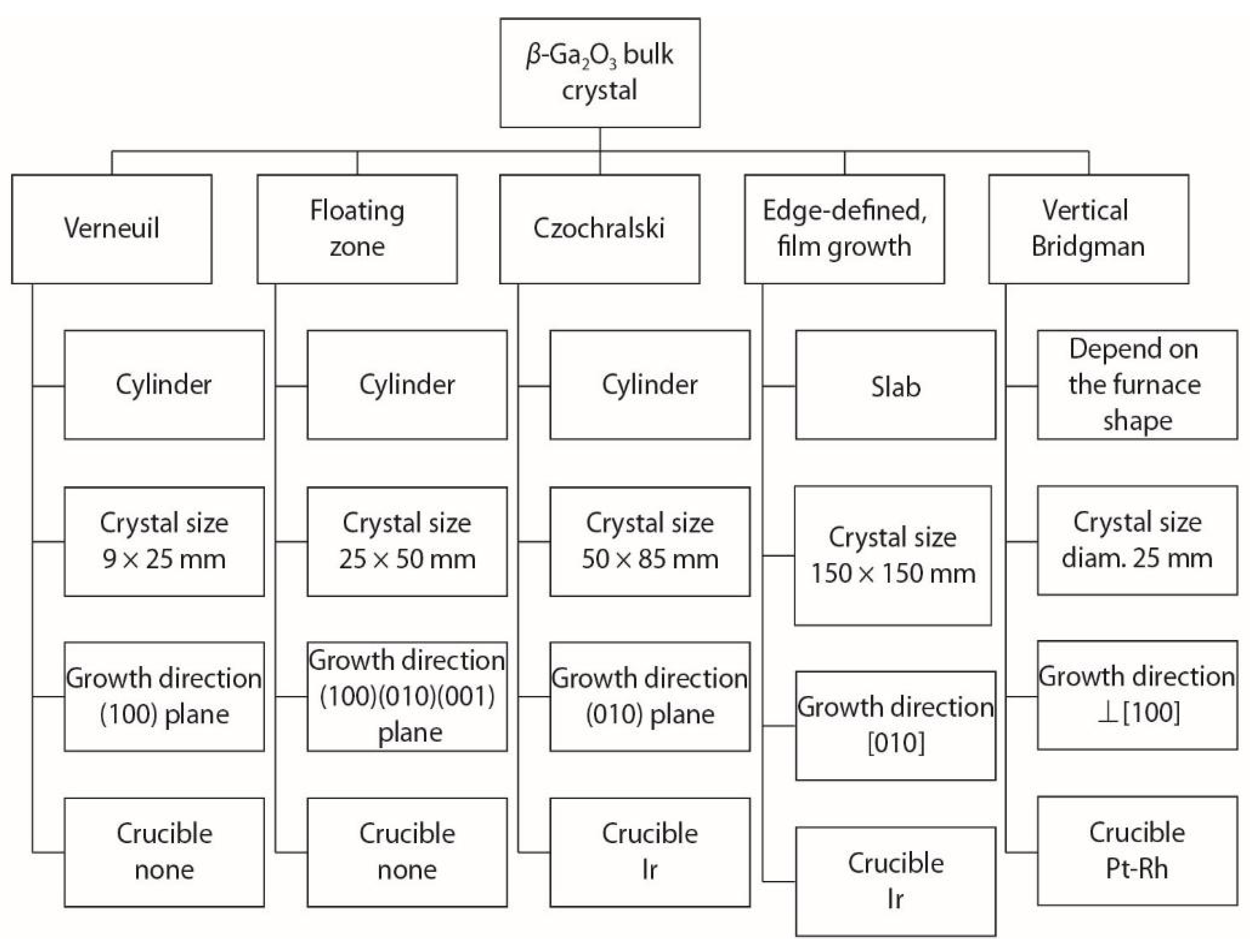
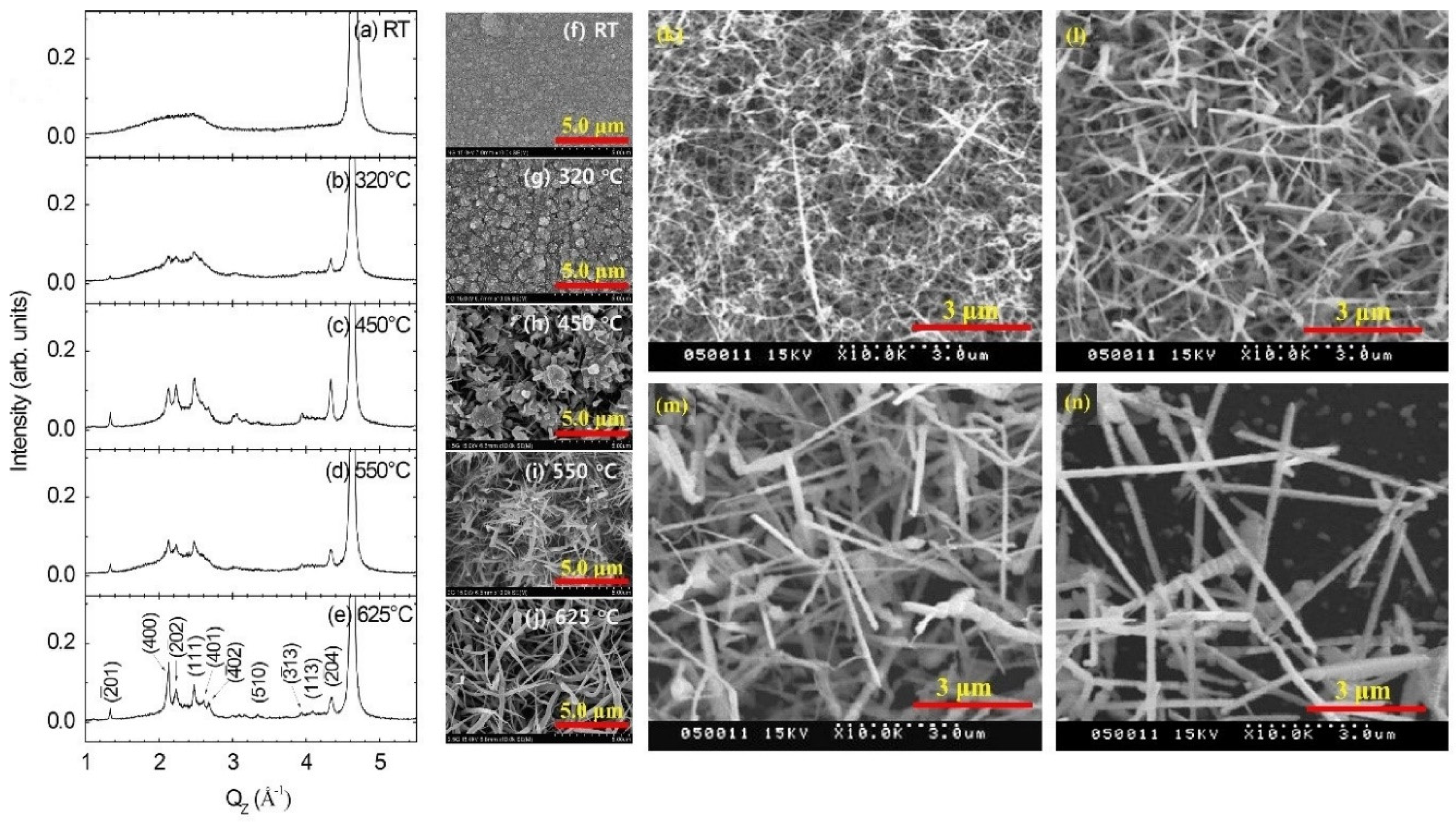
2. Structures of Gallium Oxide
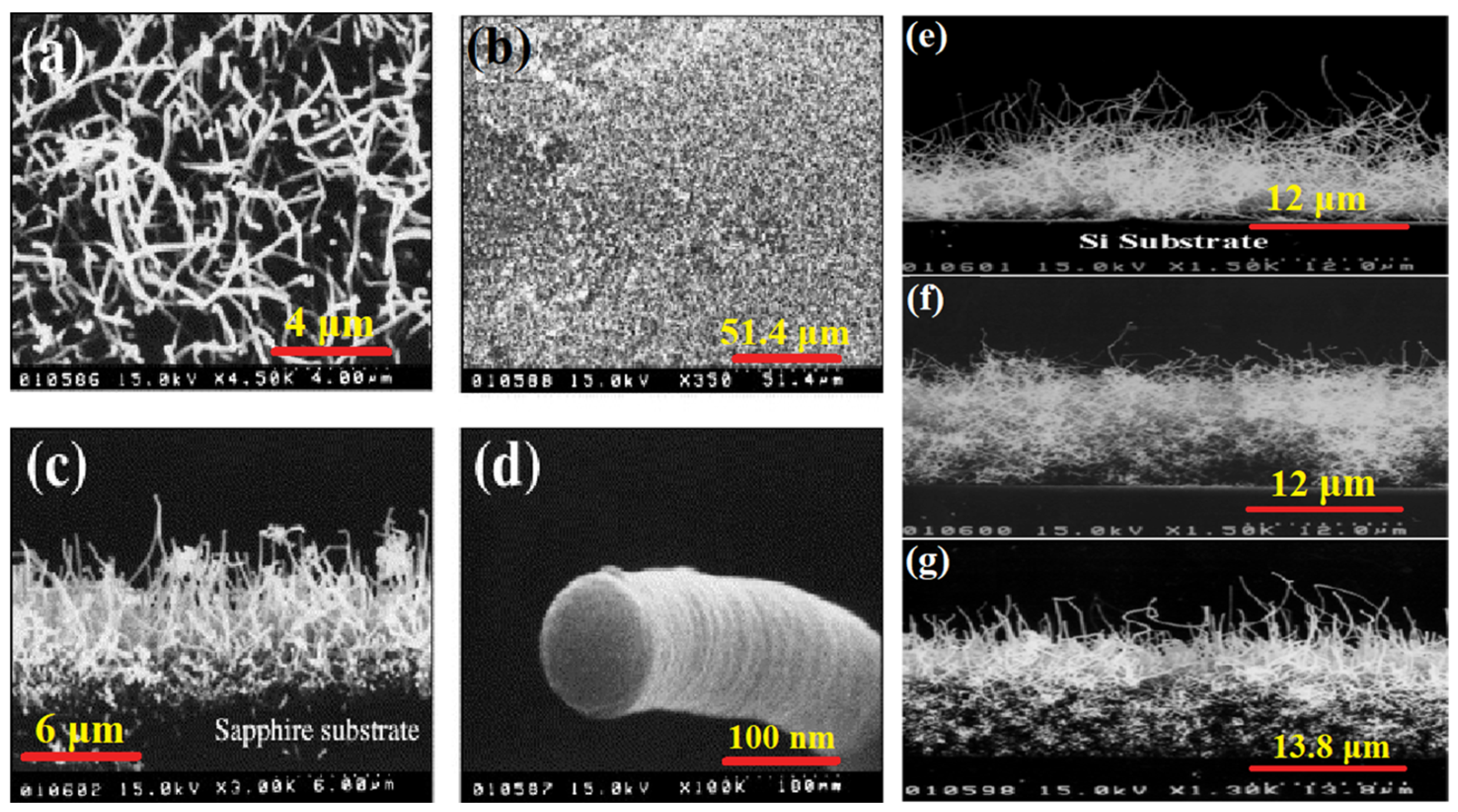
3. Synthesis of Ga2O3
3.1. Sol-Gel Method
3.2. Magnetron Sputtering
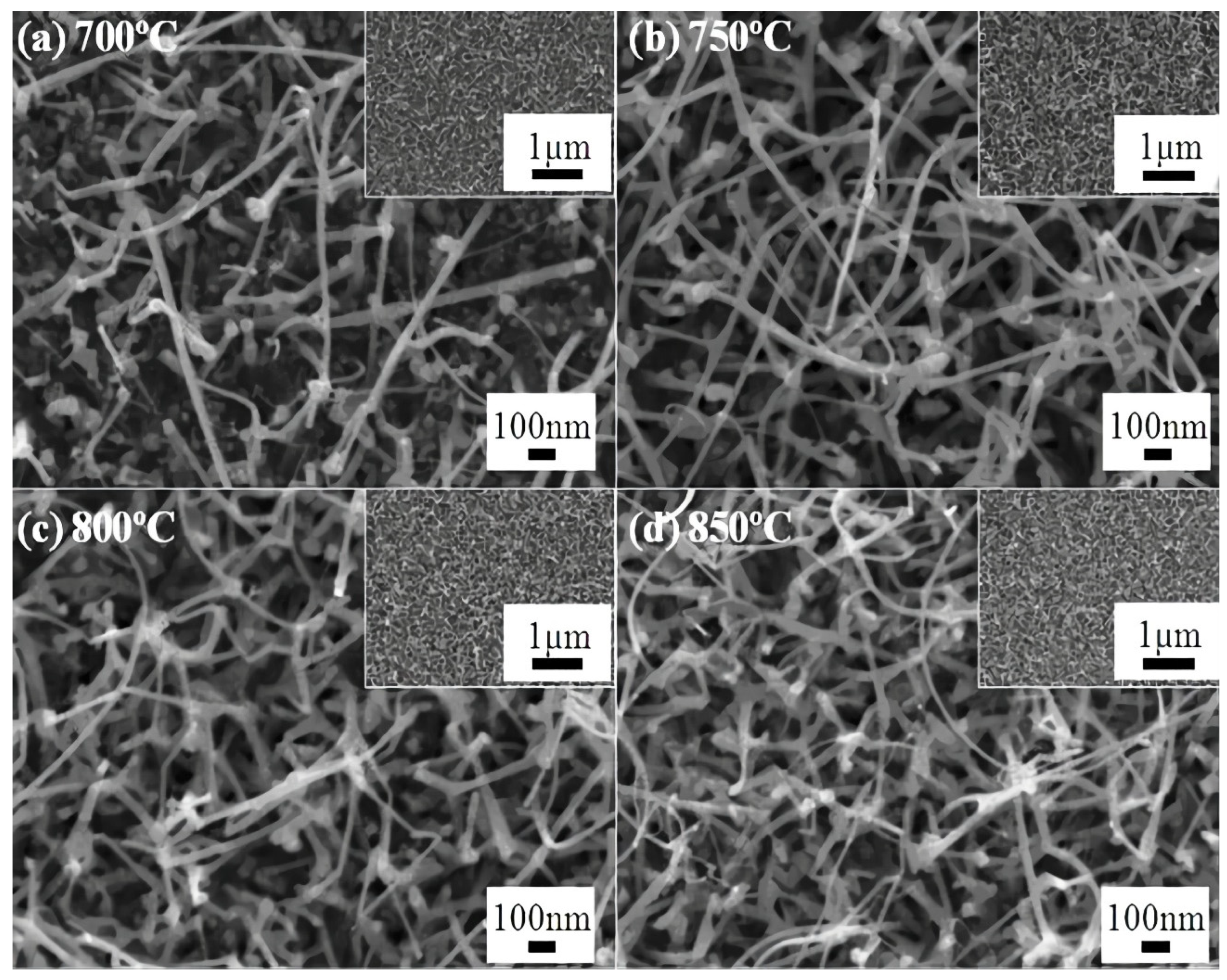
3.3. Chemical Vapor Deposition
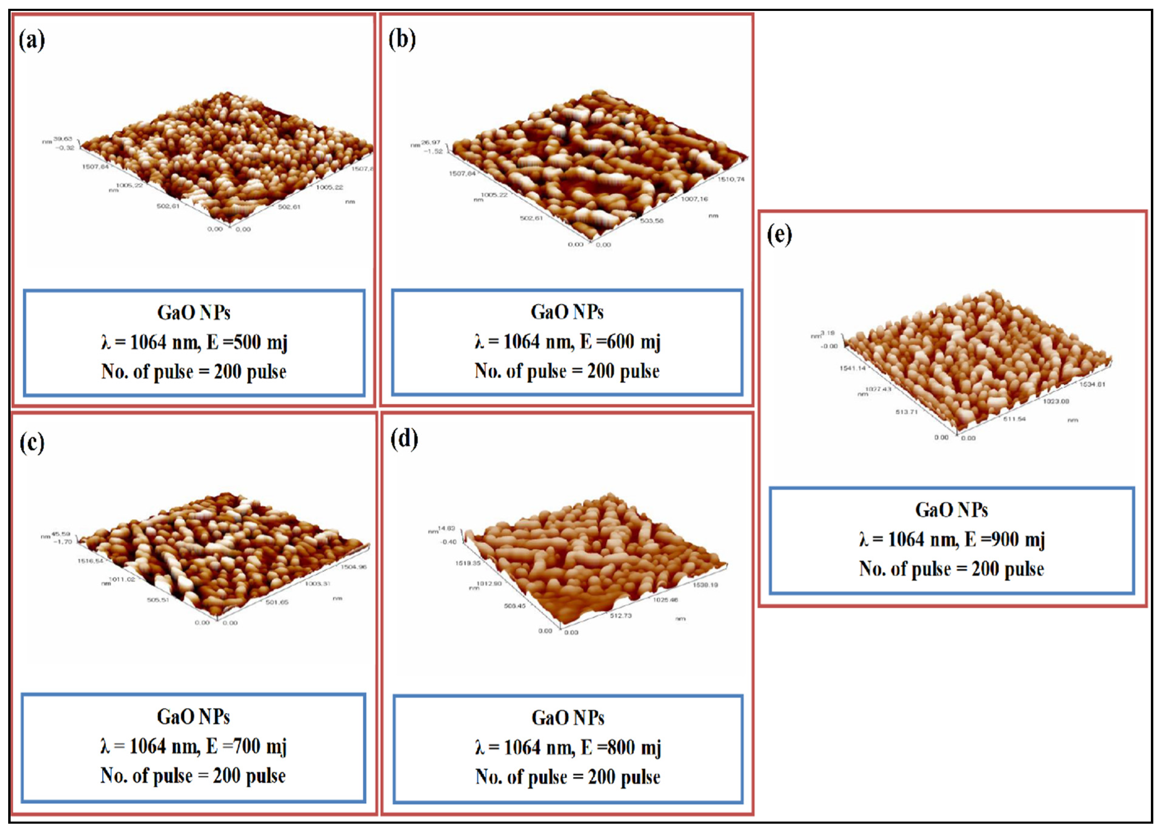
3.4. Pulsed Laser Deposition
3.5. Molecular Beam Epitaxy
4. Properties of Gallium Oxide
4.1. Optical Properties
4.1.1. Band Gap
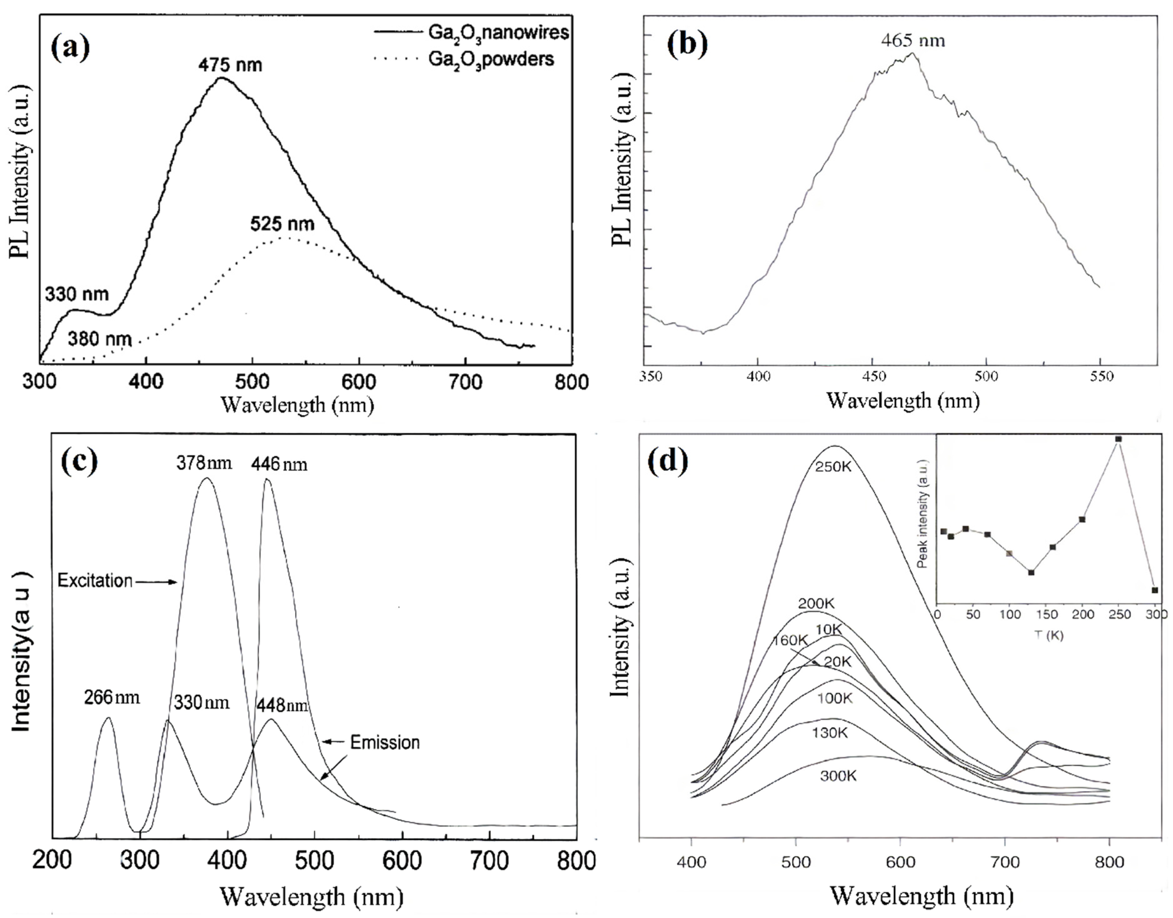
4.1.2. Photoluminescence (PL)
4.2. Electrical Properties
Photocurrent and Dark Current
5. Applications
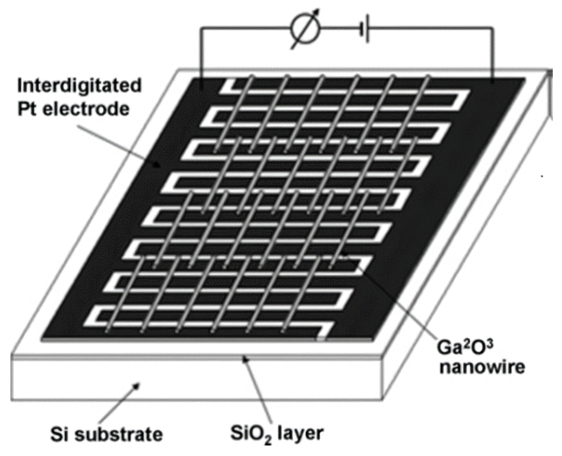
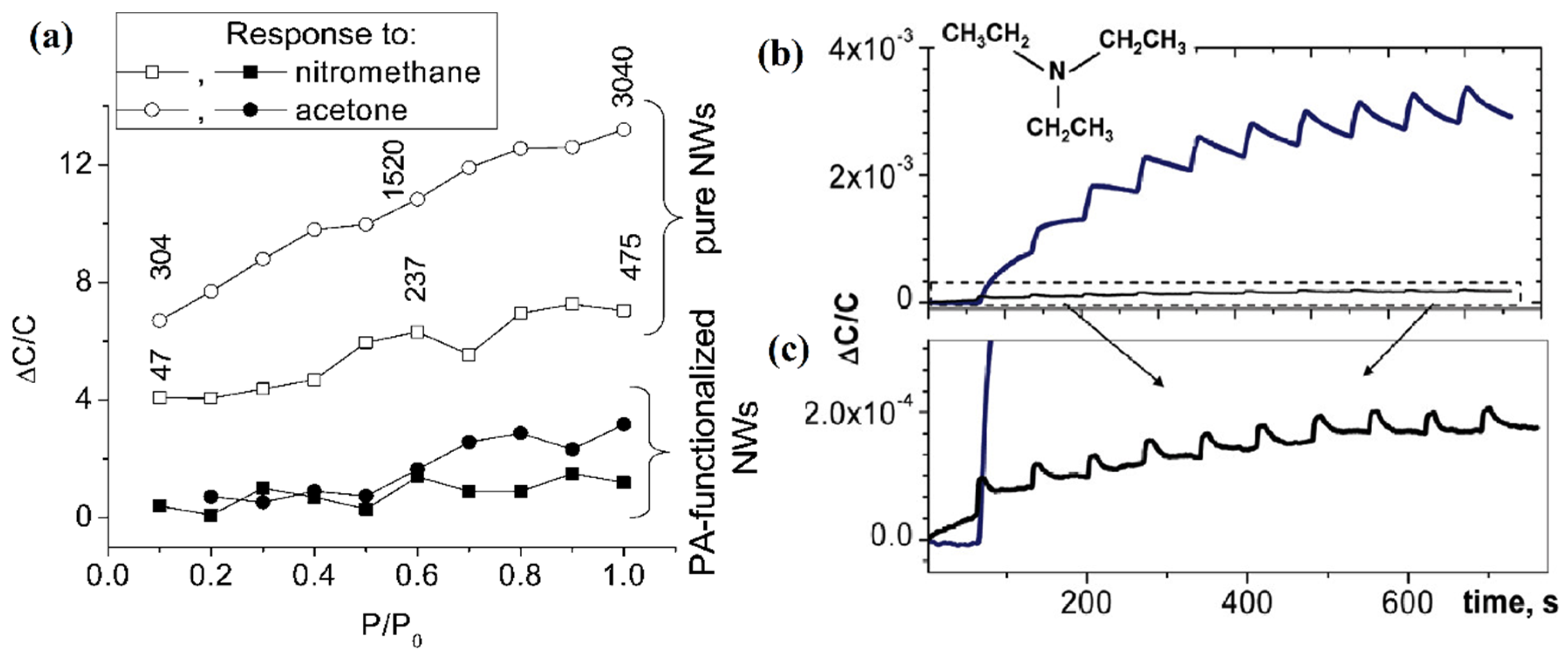
5.1. Gas Sensing Applications
5.2. Photovoltaic Devices
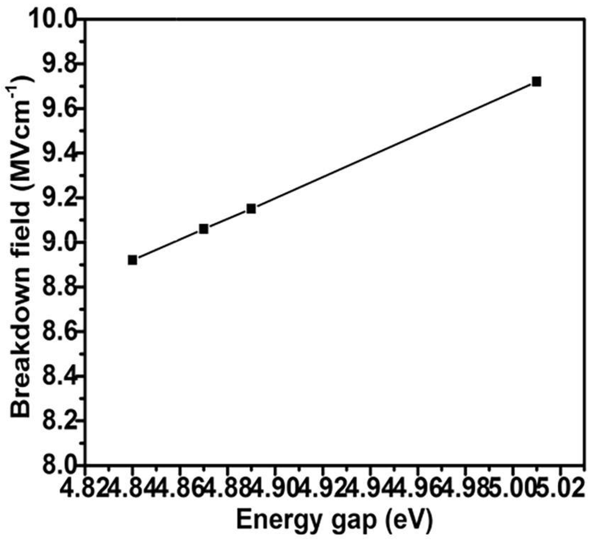
5.3. Higher Power Devices
6. Conclusions
Author Contributions
Funding
Data Availability Statement
Acknowledgments
Conflicts of Interest
References
- Higashiwaki, M.; Sasaki, K.; Kuramata, A.; Masui, T.; Yamakoshi, S. Gallium oxide (c) metal-semiconductor field-effect transistors on single-crystal β-Ga2O3 (010) substrates. Appl. Phys. Lett. 2012, 100, 013504. [Google Scholar] [CrossRef]
- Higashiwaki, M.; Sasaki, K.; Kuramata, A.; Masui, T.; Yamakoshi, S. Development of gallium oxide power devices. Phys. Status Solidi (A) 2013, 211, 21–26. [Google Scholar] [CrossRef]
- Xu, J.; Zheng, W.; Huang, F. Gallium oxide solar-blind ultraviolet photodetectors: A review. J. Mater. Chem. C 2019, 7, 8753–8770. [Google Scholar] [CrossRef]
- Rogers, A.J.; Lagally, M.G.; Nuzzo, R.G. Synthesis, assembly and applications of semiconductor nanomembranes. Nature 2011, 477, 45–53. [Google Scholar] [CrossRef] [PubMed]
- Cao, C.; Chen, Z.; An, X.; Zhu, H. Growth and Field Emission Properties of Cactus-like Gallium Oxide Nanostructures. J. Phys. Chem. C 2007, 112, 95–98. [Google Scholar] [CrossRef]
- Tippins, H. Optical absorption and photoconductivity in the band edge of β-Ga2O3. Phys. Rev. 1965, 140, A316. [Google Scholar] [CrossRef]
- Park, G.-S.; Choi, W.; Kim, J.-M.; Choi, Y.C.; Lee, Y.H.; Lim, C.-B. Structural investigation of gallium oxide (β-Ga2O3) nanowires grown by arc-discharge. J. Cryst. Growth 2000, 220, 494–500. [Google Scholar] [CrossRef]
- Choi, Y.C.; Kim, W.S.; Park, Y.S.; Lee, S.M.; Bae, D.J.; Lee, Y.H.; Park, G.S.; Choi, W.B.; Lee, N.S.; Kim, J.M. Catalytic growth of β-Ga2O3 nanowires by arc discharge. Adv. Mater. 2000, 12, 746–750. [Google Scholar] [CrossRef]
- Chun, H.J.; Choi, Y.S.; Bae, S.Y.; Seo, H.W.; Hong, A.S.J.; Park, J.; Yang, H. Controlled Structure of Gallium Oxide Nanowires. J. Phys. Chem. B 2003, 107, 9042–9046. [Google Scholar] [CrossRef]
- Gundiah, G.; Govindaraj, A.; Rao, C. Nanowires, Nanobelts and Related Nanostructures of Ga2O3. In Advances In Chemistry: A Selection of CNR Rao’s Publications (1994–2003); World Scientific: Singapore, 2003; pp. 343–348. [Google Scholar]
- Cai, K.; Shen, S.; Yan, C.; Bateman, S. Preparation, characterization and formation mechanism of gallium oxide nanowires. Curr. Appl. Phys. 2007, 8, 363–366. [Google Scholar] [CrossRef]
- Chu, S.; Majumdar, A. Opportunities and challenges for a sustainable energy future. Nature 2012, 488, 294–303. [Google Scholar] [CrossRef] [PubMed]
- Sharma, A. A comprehensive study of solar power in India and World. Renew. Sustain. Energy Rev. 2011, 15, 1767–1776. [Google Scholar] [CrossRef]
- Lee, S.H.; Kim, S.B.; Moon, Y.J.; Kim, S.M.; Jung, H.J.; Seo, M.S.; Lee, K.M.; Kim, S.K.; Lee, S.W. High-responsivity deep-ultraviolet-selective photodetectors using ultrathin gallium oxide films. ACS Photonics 2017, 4, 2937–2943. [Google Scholar] [CrossRef]
- Amano, H. Progress and Prospect of growth of wide-band-gap group iii nitrides. In III-Nitride Based Light Emitting Diodes and Applications; Springer: Berlin/Heidelberg, Germany, 2017; pp. 1–9. [Google Scholar]
- Deák, P.; Ho, Q.D.; Seemann, F.; Aradi, B.; Lorke, M.; Frauenheim, T. Choosing the correct hybrid for defect calculations: A case study on intrinsic carrier trapping in β-Ga2O3. Phys. Rev. B 2017, 95, 075208. [Google Scholar] [CrossRef]
- Liang, H.; Han, Z.; Mei, Z. Recent Progress of Deep Ultraviolet Photodetectors using Amorphous Gallium Oxide Thin Films. Phys. Status Solidi (A) 2020, 218, 2000339. [Google Scholar] [CrossRef]
- Stepanov, S.; Nikolaev, V.; Bougrov, V.; Romanov, A. Gallium OXIDE: Properties and applica 498 a review. Rev. Adv. Mater. Sci. 2016, 44, 63–86. [Google Scholar]
- Irudayadass, G. Estimation of Ionization Coefficients of Gallium Oxide for the Purpose of TCAD Simulation; University of Illinois at Chicago: Chicago, IL, USA, 2018. [Google Scholar]
- Chikoidze, E.; Fellous, A.; Perez-Tomas, A.; Sauthier, G.; Tchelidze, T.; Ton-That, C.; Huynh, T.T.; Phillips, M.; Russell, S.; Jennings, M.; et al. P-type β-gallium oxide: A new perspective for power and optoelectronic devices. Mater. Today Phys. 2017, 3, 118–126. [Google Scholar] [CrossRef] [Green Version]
- Nikolskaya, A.; Okulich, E.; Korolev, D.; Stepanov, A.; Nikolichev, D.; Mikhaylov, A.; Tetelbaum, D.; Almaev, A.; Bolzan, C.A.; Buaczik, A., Jr.; et al. Ion implantation in β-Ga2O3: Physics and technology. J. Vac. Sci. Technol. A Vac. Surf. Films 2021, 39, 030802. [Google Scholar] [CrossRef]
- Fine, G.F.; Cavanagh, L.M.; Afonja, A.; Binions, R. Metal Oxide Semi-Conductor Gas Sensors in Environmental Monitoring. Sensors 2010, 10, 5469–5502. [Google Scholar] [CrossRef] [Green Version]
- Moseley, P. Materials selection for semiconductor gas sensors. Sens. Actuators B Chem. 1992, 6, 149–156. [Google Scholar] [CrossRef]
- Fergus, J.W. Perovskite oxides for semiconductor-based gas sensors. Sens. Actuators B Chem. 2007, 123, 1169–1179. [Google Scholar] [CrossRef]
- Moos, R.; Izu, N.; Rettig, F.; Reiß, S.; Shin, W.; Matsubara, I. Resistive Oxygen Gas Sensors for Harsh Environments. Sensors 2011, 11, 3439–3465. [Google Scholar] [CrossRef] [PubMed] [Green Version]
- Afzal, A. β-Ga2O3 nanowires and thin films for metal oxide semiconductor gas sensors: Sensing mechanisms and performance enhancement strategies. J. Mater. 2019, 5, 542–557. [Google Scholar] [CrossRef]
- Jubu, P.R.; Yam, F. Influence of growth duration and nitrogen-ambient on the morphological and structural properties of beta-gallium oxide micro- and nanostructures. Mater. Chem. Phys. 2019, 239, 122043. [Google Scholar] [CrossRef]
- Glaudell, A.M.; Cochran, J.E.; Patel, S.N.; Chabinyc, M.L. Impact of the Doping Method on Conductivity and Thermopower in Semiconducting Polythiophenes. Adv. Energy Mater. 2014, 5, 1401072. [Google Scholar] [CrossRef]
- Pfeiffer, M.; Leo, K.; Zhou, X.; Huang, J.; Hofmann, M.; Werner, A.; Blochwitz-Nimoth, J. Doped organic semiconductors: Physics and application in light emitting diodes. Org. Electron. 2003, 4, 89–103. [Google Scholar] [CrossRef]
- Moser, M.; Fajardo, T., Jr.; Wadsworth, A.; Giovannitti, A.; McCulloch, I. Materials in organic electrochemical transistors for bioelectronic applications: Past, present, and future. Adv. Funct. Mater. 2019, 29, 1807033. [Google Scholar] [CrossRef]
- Baliga, B.J. Gallium nitride devices for power electronic applications. Semicond. Sci. Technol. 2013, 28, 074011. [Google Scholar] [CrossRef]
- Matsunami, H. Current SiC technology for power electronic devices beyond Si. Microelectron. Eng. 2006, 83, 2–4. [Google Scholar] [CrossRef]
- Heywang, W.; Zaininger, K.H. Silicon: The Semiconductor Material. In Silicon; Springer: Berlin/Heidelberg, Germany, 2004; pp. 25–42. [Google Scholar]
- Baliga, B. The future of power semiconductor device technology. Proc. IEEE 2001, 89, 822–832. [Google Scholar] [CrossRef]
- Rocha, C.; Galvão, H.; Barbosa, A. Role of transient silicon limitation in the development of cyanobacteria blooms in the Guadiana estuary, south-western Iberia. Mar. Ecol. Prog. Ser. 2002, 228, 35–45. [Google Scholar] [CrossRef] [Green Version]
- Melton, A.G. Development of Wide Bandgap Solid-State Neutron Detectors. Ph.D. Thesis, Georgia Institute of Technology, Atlanta, GA, USA, 2011. [Google Scholar]
- Grummel, B. Design and Characterization of High Temperature Packaging for Wide-Bandgap Semiconductor Devices. Ph.D. Thesis, University of Central Florida, Orlando, FL, USA, 2012. [Google Scholar]
- Pan, Z.; Lai, H.L.; Au, F.C.; Duan, X.; Zhou, W.; Shi, W.; Wang, N.; Lee, C.S.; Wong, N.B.; Lee, S.T.; et al. Oriented silicon carbide nanowires: Synthesis and field emission properties. Adv. Mater. 2000, 12, 1186–1190. [Google Scholar] [CrossRef]
- Cheng, G.; Chang, T.-H.; Qin, Q.; Huang, H.; Zhu, Y. Mechanical Properties of Silicon Carbide Nanowires: Effect of Size-Dependent Defect Density. Nano Lett. 2014, 14, 754–758. [Google Scholar] [CrossRef] [PubMed]
- Chen, C.C.; Yeh, C.C.; Chen, C.H.; Yu, M.Y.; Liu, H.L.; Wu, J.J.; Chen, K.H.; Chen, L.C.; Peng, J.Y.; Chen, Y.F. Catalytic growth and characterization of gallium nitride nanowires. J. Am. Chem. Soc. 2001, 123, 2791–2798. [Google Scholar] [CrossRef] [PubMed]
- Ganguly, B.N.; Verma, V.; Chatterjee, D.; Satpati, B.; Debnath, S.; Saha, P. Study of Gallium Oxide Nanoparticles Conjugated with β-Cyclodextrin: An Application To Combat Cancer. ACS Appl. Mater. Interfaces 2016, 8, 17127–17137. [Google Scholar] [CrossRef] [PubMed]
- Shi, F.; Qiao, H. Preparations, properties and applications of gallium oxide nanomaterials–A review. Nano Sel. 2022, 3, 348–373. [Google Scholar] [CrossRef]
- Yan, J.; Lu, Y.; Chen, G.; Yang, M.; Gu, Z. Advances in liquid metals for biomedical applications. Chem. Soc. Rev. 2018, 47, 2518–2533. [Google Scholar] [CrossRef]
- Latifa Chowdhury, M. Hybridization of Gallium Oxide with Magnetic Graphene Oxide toward a Low Cost and Reusable Photocatalyst. Master’s Thesis, Bangladesh University of Engineering and Technology, Dhaka, Bangladesh, 2018. [Google Scholar]
- Rana, K.S.; Souza, L.; Isaacs, M.A.; Raja, F.N.S.; Morrell, A.P.; Martin, R.A. Development and Characterization of Gallium-Doped Bioactive Glasses for Potential Bone Cancer Applications. ACS Biomater. Sci. Eng. 2017, 3, 3425–3432. [Google Scholar] [CrossRef]
- Niederberger, M.; Garnweitner, G. Organic Reaction Pathways in the Nonaqueous Synthesis of Metal Oxide Nanoparticles. Chem. A Eur. J. 2006, 12, 7282–7302. [Google Scholar] [CrossRef]
- Chen, X.; Ren, F.; Gu, S.; Ye, J. Review of gallium-oxide-based solar-blind ultraviolet photodetectors. Photonics Res. 2019, 7, 381–415. [Google Scholar] [CrossRef]
- Banger, K.K.; Yamashita, Y.; Mori, K.; Peterson, R.L.; Leedham, T.; Rickard, J.; Sirringhaus, H.J.N.M. Low-temperature, high-performance solution-processed metal oxide thin-film transistors formed by a ‘sol–gel on chip’ process. Nat. Mater. 2011, 10, 45–50. [Google Scholar] [CrossRef] [PubMed]
- Bosi, M.; Mazzolini, P.; Seravalli, L.; Fornari, R. Ga2O3 polymorphs: Tailoring the epitaxial growth conditions. J. Mater. Chem. C 2020, 8, 10975–10992. [Google Scholar] [CrossRef]
- Åhman, J.; Svensson, G.; Albertsson, J. A reinvestigation of β-gallium oxide. Acta Crystallogr. Sect. C Cryst. Struct. Commun. 1996, 52, 1336–1338. [Google Scholar] [CrossRef] [Green Version]
- Yang, D.; Kim, B.; Eom, T.H.; Park, Y.; Jang, H.W. Epitaxial Growth of Alpha Gallium Oxide Thin Films on Sapphire Substrates for Electronic and Optoelectronic Devices: Progress and Perspective. Electron. Mater. Lett. 2022, 18, 113–128. [Google Scholar] [CrossRef]
- Roy, R.; Hill, V.G.; Osborn, E.F. Polymorphism of Ga2O3 and the system Ga2O3—H2O. J. Am. Chem. Soc. 1952, 74, 719–722. [Google Scholar] [CrossRef]
- Lee, S.; Akaiwa, K.; Fujita, S. Thermal stability of single crystalline alpha gallium oxide films on sapphire substrates. Phys. Status Solidi (C) 2013, 10, 1592–1595. [Google Scholar] [CrossRef]
- Higashiwaki, M.; Sasaki, K.; Murakami, H.; Kumagai, Y.; Koukitu, A.; Kuramata, A.; Masui, T.; Yamakoshi, S. Recent progress in Ga2O3 power devices. Semicond. Sci. Technol. 2016, 31, 034001. [Google Scholar] [CrossRef]
- Higashiwaki, M.; Jessen, G.H. Guest Editorial: The dawn of gallium oxide microelectronics. Appl. Phys. Lett. 2018, 112, 060401. [Google Scholar] [CrossRef] [Green Version]
- Xiao, H.-D.; Ma, H.-L.; Xue, C.-S.; Zhuang, H.-Z.; Ma, J.; Zong, F.-J.; Zhang, X.-J. Synthesis and structural properties of beta-gallium oxide particles from gallium nitride powder. Mater. Chem. Phys. 2007, 101, 99–102. [Google Scholar] [CrossRef]
- Pichorim, A.; Costa, D.; Neckel, I.; Mosca, D. Non-stoichiometric gallium oxide with cubic structure directly integrated to C-Cut sapphire. Mater. Sci. Semicond. Process. 2021, 139, 106349. [Google Scholar] [CrossRef]
- Sharma, A.; Varshney, M.; Saraswat, H.; Chaudhary, S.; Parkash, J.; Shin, H.J.; Chae, K.H.; Won, S.O. Nano-structured phases of gallium oxide (GaOOH, α-Ga2O3, β-Ga2O3, γ-Ga2O3, δ-Ga2O3, and ε-Ga2O3): Fabrication, structural, and electronic structure investigations. Int. Nano Lett. 2020, 10, 71–80. [Google Scholar] [CrossRef]
- Mulazzi, M.; Reichmann, F.; Becker, A.; Klesse, W.M.; Alippi, P.; Fiorentini, V.; Parisini, A.; Bosi, M.; Fornari, R. The electronic structure of ε-Ga2O3. APL Mater. 2019, 7, 022522. [Google Scholar] [CrossRef] [Green Version]
- Yoshioka, S.; Hayashi, H.; Kuwabara, A.; Oba, F.; Matsunaga, K.; Tanaka, I. Structures and energetics of Ga2O3 polymorphs. J. Phys. Condens. Matter 2007, 19, 346211. [Google Scholar] [CrossRef]
- Zhao, X.; Ding, M.; Sun, H.; Long, S. Controlling different phases of gallium oxide for solar-blind photodetector application. Semicond. Semimet. 2021, 107, 101–151. [Google Scholar] [CrossRef]
- Playford, H.Y.; Hannon, A.C.; Barney, E.R.; Walton, R.I. Structures of uncharacterised polymorphs of gallium oxide from total neutron diffraction. Chem. A Eur. J. 2013, 19, 2803–2813. [Google Scholar] [CrossRef] [PubMed]
- García-Carrión, M.; Ramírez-Castellanos, J.; Nogales, E.; Méndez, B.; You, C.C.; Karazhanov, S.; Marstein, E.S. Hybrid solar cells with β-and γ-gallium oxide nanoparticles. Mater. Lett. 2020, 261, 127088. [Google Scholar] [CrossRef]
- Gutiérrez, Y.; García-Fernández, P.; Junquera, J.; Brown, A.S.; Moreno, F.; Losurdo, M. Polymorphic gallium for active resonance tuning in photonic nanostructures: From bulk gallium to two-dimensional (2D) gallenene. Nanophotonics 2020, 9, 4233–4252. [Google Scholar] [CrossRef]
- Pratiyush, A.S.; Muazzam, U.U.; Kumar, S.; Vijayakumar, P.; Ganesamoorthy, S.; Subramanian, N.; Nath, D.N. Optical Float-Zone Grown Bulk beta-Ga2O3-Based Linear MSM Array of UV-C Photodetectors. IEEE Photonics Technol. Lett. 2019, 31, 923–926. [Google Scholar] [CrossRef]
- Nikolaev, V.; Maslov, V.; Stepanov, S.; Pechnikov, A.; Krymov, V.; Nikitina, I.; Guzilova, L.; Bougrov, V.; Romanov, A. Growth and characterization of β-Ga2O3 crystals. J. Cryst. Growth 2017, 457, 132–136. [Google Scholar] [CrossRef]
- Dhanabalan, D.; Ananthu, V.; Akshita, K.V.; Bhattacharya, S.; Varadarajan, E.; Ganesamoorthy, S. Studies on Schottky Barrier Diodes Fabricated using Single-Crystal Wafers of β-Ga2O3 Grown by the Optical Floating Zone Technique. Phys. Status Solidi (B) 2022, 259, 2100496. [Google Scholar] [CrossRef]
- Blevins, J.D.; Chabak, K.; Jessen, G.; Thomson, D.; Stevens, K.; Foundos, G.; Lindsey, A.; Leach, J.H.; Rumsey, J.; Green, A. Growth of 50mm beta-gallium oxide (β-Ga2O3) substrates. In Proceedings of the CS Mantech 2018—International Conference on Compound Semiconductor and Manufacturing Technology, Austin, TX, USA, 7–10 May 2018. [Google Scholar]
- Bauman, D.; Borodkin, A.; Petrenko, A.; Panov, D.; Kremleva, A.; Spiridonov, V.; Zakgeim, D.; Silnikov, M.; Odnoblyudov, M.; Romanov, A.; et al. On improving the radiation resistance of gallium oxide for space applications. Acta Astronaut. 2020, 180, 125–129. [Google Scholar] [CrossRef]
- Galazka, Z. Czochralski Method. In Gallium Oxide; Springer: Berlin/Heidelberg, Germany, 2020; pp. 15–36. [Google Scholar]
- Tao, X. Bulk gallium oxide single crystal growth. J. Semicond. 2019, 40, 010401. [Google Scholar] [CrossRef]
- Bayraktaroglu, B. Assessment of Gallium Oxide Technology; Air Force Research Laboratory, Sensors Directorate WPAFB United States: Wright-Patterson AFB, OH, USA, 2017. [Google Scholar]
- Higashiwaki, M.; Fujita, S. Gallium Oxide: Materials Properties, Crystal Growth, and Devices; Springer Nature: Berlin, Germany, 2020. [Google Scholar]
- Blevins, J.; Thomson, D.; Stevens, K.; Foundos, G. Growth of single crystal beta-gallium oxide (β-Ga2O3) semiconductor material. In Proceedings of the CSMANTECH, Indian wells, CA, USA, 22–25 May 2017. [Google Scholar]
- Blevins, J.; Stevens, K.; Lindsey, A.; Foundos, G.; Sande, L. Development of large diameter semi-insulating gallium oxide (Ga2O3) substrates. IEEE Trans. Semicond. Manuf. 2019, 32, 466–472. [Google Scholar] [CrossRef]
- Park, J.; Hong, S.-M. Simulation Study of Enhancement Mode Multi-Gate Vertical Gallium Oxide MOSFETs. ECS J. Solid State Sci. Technol. 2019, 8, Q3116–Q3121. [Google Scholar] [CrossRef]
- Kuramata, A.; Koshi, K.; Watanabe, S.; Yamaoka, Y.; Masui, T.; Yamakoshi, S. Bulk crystal growth of Ga2O3 in Oxide-based Materials and Devices IX. Int. Soc. Opt. Photonics 2018, 10533, 105330E. [Google Scholar]
- Mohamed, H.; Xia, C.; Sai, Q.; Cui, H.; Pan, M.; Qi, H. Growth and fundamentals of bulk β-Ga2O3 single crystals. J. Semicond. 2019, 40, 011801. [Google Scholar] [CrossRef]
- Dislich, H. Sol-gel: Science, processes and products. J. Non-Cryst. Solids. 1986, 80, 115–121. [Google Scholar] [CrossRef]
- Ji, W.; Zhao, Y.; Fahad, H.M.; Bullock, J.; Allen, T.; Lien, D.-H.; De Wolf, S.; Javey, A. Dip Coating Passivation of Crystalline Silicon by Lewis Acids. ACS Nano 2019, 13, 3723–3729. [Google Scholar] [CrossRef]
- Adhikari, B.; Majumdar, S. Polymers in sensor applications. Prog. Polym. Sci. 2004, 29, 699–766. [Google Scholar] [CrossRef]
- Gallant, B.M.; Gu, X.W.; Chen, D.Z.; Greer, J.R.; Lewis, N.S. Tailoring of Interfacial Mechanical Shear Strength by Surface Chemical Modification of Silicon Microwires Embedded in Nafion Membranes. ACS Nano 2015, 9, 5143–5153. [Google Scholar] [CrossRef] [Green Version]
- Miyata, T.; Nakatani, T.; Minami, T. Manganese-activated gallium oxide electroluminescent phosphor thin films prepared using various deposition methods. Thin Solid Film. 2000, 373, 145–149. [Google Scholar] [CrossRef]
- Sinha, G.; Ganguli, D.; Chaudhuri, S. Crystallization and optical properties of finite sized β-Ga2O3 in sol–gel derived Ga2O3:SiO2nanocomposites. J. Phys. Condens. Matter 2006, 18, 11167–11176. [Google Scholar] [CrossRef]
- Pye, M.; Birtill, J.; Dickens, P. α-Gallium oxide deuteriohydroxide: A powder neutron diffraction investigation. Acta Crystallogr. Sect. B Struct. Crystallogr. Cryst. Chem. 1977, 33, 3224–3226. [Google Scholar] [CrossRef] [Green Version]
- Taş, A.C.; Majewski, P.J.; Aldinger, F. Synthesis of Gallium Oxide Hydroxide Crystals in Aqueous Solutions with or without Urea and Their Calcination Behavior. J. Am. Ceram. Soc. 2002, 85, 1421–1429. [Google Scholar] [CrossRef] [Green Version]
- Nayak, S.; Lyon, L.A. Soft Nanotechnology with Soft Nanoparticles. Angew. Chem. Int. Ed. 2005, 44, 7686–7708. [Google Scholar] [CrossRef] [PubMed]
- Ciriminna, R.; Fidalgo, A.; Pandarus, V.; Béland, F.; Ilharco, L.M.; Pagliaro, M. The Sol–Gel Route to Advanced Silica-Based Materials and Recent Applications. Chem. Rev. 2013, 113, 6592–6620. [Google Scholar] [CrossRef]
- Liu, X.; Qiu, G.; Zhao, Y.; Zhang, N.; Yi, R. Gallium oxide nanorods by the conversion of gallium oxide hydroxide nanorods. J. Alloys Compd. 2007, 439, 275–278. [Google Scholar] [CrossRef]
- Quan, Y.; Fang, D.; Zhang, X.; Liu, S.; Huang, K. Synthesis and characterization of gallium oxide nanowires via a hydrothermal method. Mater. Chem. Phys. 2010, 121, 142–146. [Google Scholar] [CrossRef]
- Gopal, R.; Goyal, A.; Saini, A.; Nagar, M.; Sharma, N.; Gupta, D.K.; Dhayal, V. Sol-gel synthesis of Ga2O3 nanorods and effect of precursor chemistry on their structural and morphological properties. Ceram. Int. 2018, 44, 19099–19105. [Google Scholar] [CrossRef]
- Qian, L.-X.; Wu, Z.-H.; Zhang, Y.-Y.; Lai, P.T.; Liu, X.-Z.; Li, Y.-R. Ultrahigh-Responsivity, Rapid-Recovery, Solar-Blind Photodetector Based on Highly Nonstoichiometric Amorphous Gallium Oxide. ACS Photon. 2017, 4, 2203–2211. [Google Scholar] [CrossRef]
- Saikumar, A.K.; Sundaresh, S.; Nehate, S.D.; Sundaram, K.B. Preparation and Characterization of Radio Frequency Sputtered Delafossite p-type Copper Gallium Oxide (p-CuGaO2) Thin Films. ECS J. Solid State Sci. Technol. 2022, 11, 023005. [Google Scholar] [CrossRef]
- Takeuchi, T.; Ishikawa, H.; Takeuchi, N.; Horikoshi, Y. High resolution X-ray photoelectron spectroscopy of beta gallium oxide films deposited by ultra-high vacuum radio frequency magnetron sputtering. Thin Solid Films 2008, 516, 4593–4597. [Google Scholar] [CrossRef]
- Mobtakeri, S.; Tuzemen, E.S.; Ali, Ö.; Emre, G. Characterization of Gallium Oxide/glass thin films grown by RF magnetron sputtering. Cumhur. Sci. J. 2020, 41, 929–937. [Google Scholar] [CrossRef]
- Yang, L.; Xue, C.; Wang, C.; Li, H. Growth of GaN nanowires by ammoniating Ga2O3 thin films deposited on quartz with radio frequency magnetron sputtering. Nanotechnology 2002, 14, 50–52. [Google Scholar] [CrossRef]
- Kumar, S.S.; Rubio, E.; Noor-A-Alam, M.; Martinez, G.; Manandhar, S.; Shutthanandan, V.; Thevuthasan, S.; Ramana, C. Structure, Morphology, and Optical Properties of Amorphous and Nanocrystalline Gallium Oxide Thin Films. J. Phys. Chem. C 2013, 117, 4194–4200. [Google Scholar] [CrossRef]
- Ogita, M.; Higo, K.; Nakanishi, Y.; Hatanaka, Y. Ga2O3 thin film for oxygen sensor at high temperature. Appl. Surf. Sci. 2001, 175, 721–725. [Google Scholar] [CrossRef]
- Gutierrez, G.; Sundin, E.M.; Nalam, P.G.; Zade, V.; Romero, R.; Nair, A.N.; Sreenivasan, S.; Das, D.; Li, C.; Ramana, C.V. Interfacial Phase Modulation-Induced Structural Distortion, Band Gap Reduction, and Nonlinear Optical Activity in Tin-Incorporated Ga2O3. J. Phys. Chem. C 2021, 125, 20468–20481. [Google Scholar] [CrossRef]
- Wang, J.; Zhuang, H.; Zhang, X.; Zhang, S.; Li, J. Synthesis and properties of β-Ga2O3 nanostructures. Vacuum 2011, 85, 802–805. [Google Scholar] [CrossRef]
- Lee, S.; Kang, H. Synthesis and characterization of β-Ga2O3 nanowires on amorphous substrates using radio-frequency powder sputtering. J. Cryst. Growth 2015, 412, 25–30. [Google Scholar] [CrossRef]
- Singh, A.K.; Gupta, M.; Sathe, V.; Katharria, Y. Effect of annealing temperature on β-Ga2O3 thin films deposited by RF sputtering method. Superlattices Microstruct. 2021, 156, 106976. [Google Scholar] [CrossRef]
- Hedei, P.H.M.A.; Hassan, Z.; Quah, H.J. Effects of post-deposition annealing temperature in nitrogen/oxygen/nitrogen ambient on polycrystalline gallium oxide films. Appl. Surf. Sci. 2021, 550, 149340. [Google Scholar] [CrossRef]
- Lee, S.H.; Lee, S.; Jang, S.C.; On, N.; Kim, H.-S.; Jeong, J.K. Mobility enhancement of indium-gallium oxide via oxygen diffusion induced by a metal catalytic layer. J. Alloys Compd. 2020, 862, 158009. [Google Scholar] [CrossRef]
- Jubu, P.; Yam, F.; Obaseki, O.; Yusof, Y. Synthesis and characterization of gallium oxide in strong reducing growth ambient by chemical vapor deposition. Mater. Sci. Semicond. Process. 2020, 121, 105361. [Google Scholar] [CrossRef]
- Rubio, E.; Mates, T.; Manandhar, S.; Nandasiri, M.; Shutthanandan, V.; Ramana, C. Tungsten incorporation into gallium oxide: Crystal structure, surface and interface chemistry, thermal stability, and interdiffusion. J. Phys. Chem. C 2016, 120, 26720–26735. [Google Scholar] [CrossRef]
- Kumar, S.; Tessarek, C.; Sarau, G.; Christiansen, S.; Singh, R. Self-Catalytic Growth of β-Ga2O3 Nanostructures by Chemical Vapor Deposition. Adv. Eng. Mater. 2015, 17, 709–715. [Google Scholar] [CrossRef]
- Chen, M.-I.; Singh, A.; Chiang, J.-L.; Horng, R.-H.; Wuu, D.-S. Zinc Gallium Oxide—A Review from Synthesis to Applications. Nanomaterials 2020, 10, 2208. [Google Scholar] [CrossRef]
- Kumar, U.; Yadav, B. Synthesis of carbon nanotubes by direct liquid injection chemical vapor deposition method and its relevance for developing an ultra-sensitive room temperature based CO2 sensor. J. Taiwan Inst. Chem. Eng. 2019, 96, 652–663. [Google Scholar] [CrossRef]
- Hosein, I.D.; Hegde, M.; Jones, P.D.; Chirmanov, V.; Radovanovic, P.V. Evolution of the faceting, morphology and aspect ratio of gallium oxide nanowires grown by vapor–solid deposition. J. Cryst. Growth 2014, 396, 24–32. [Google Scholar] [CrossRef]
- Terasako, T.; Ichinotani, H.; Yagi, M. Growth of β-gallium oxide films and nanostructures by atmospheric-pressure CVD using gallium and water as source materials. Phys. Status Solidi (C) 2015, 12, 985–988. [Google Scholar] [CrossRef]
- Binions, R.; Carmalt, C.; Parkin, I.; Pratt, A.K.F.E.; Shaw, G.A. Gallium Oxide Thin Films from the Atmospheric Pressure Chemical Vapor Deposition Reaction of Gallium Trichloride and Methanol. Chem. Mater. 2004, 16, 2489–2493. [Google Scholar] [CrossRef]
- Valet, M.; Hoffman, D.M. Synthesis of Homoleptic Gallium Alkoxide Complexes and the Chemical Vapor Deposition of Gallium Oxide Films. Chem. Mater. 2001, 13, 2135–2143. [Google Scholar] [CrossRef]
- Mîinea, L.; Suh, S.; Bott, S.G.; Liu, J.-R.; Chu, W.-K.; Hoffman, D.M. Synthesis of aluminium and gallium fluoroalkoxide compounds and the low pressure metal-organic chemical vapor deposition of gallium oxide films. J. Mater. Chem. 1999, 9, 929–935. [Google Scholar] [CrossRef]
- Zardo, I.; Yu, L.; Conesa-Boj, S.; Estradé, S.; Alet, P.J.; Rössler, J.; Frimmer, M.; I Cabarrocas, P.R.; Peiró, F.; Arbiol, J.; et al. Gallium assisted plasma enhanced chemical vapor deposition of silicon nanowires. Nanotechnology 2009, 20, 155602. [Google Scholar] [CrossRef] [PubMed] [Green Version]
- Hellwig, M.; Xu, K.; Barreca, D.; Gasparotto, A.; Niermann, B.; Winter, J.; Becker, H.-W.; Rogalla, D.; Fischer, R.; Devi, A. MOCVD of gallium oxide thin films using homoleptic gallium complexes: Precursor evaluation and thin film characterisation. ECS Trans. 2009, 25, 617. [Google Scholar] [CrossRef]
- Kim, H.W.; Kim, N.H. MOCVD Growth and Annealing of Gallium Oxide Thin Film and Its Structural Characterization. In Materials Science Forum; Trans Tech Publications: Zurich, Switzerland, 2005; Volume 475, pp. 3377–3380. [Google Scholar]
- Park, J.-H.; McClintock, R.; Razeghi, M. Ga2O3 metal-oxide-semiconductor field effect transistors on sapphire substrate by MOCVD. Semicond. Sci. Technol. 2019, 34, 08LT01. [Google Scholar] [CrossRef]
- Yang, F. Modern Metal-Organic Chemical Vapor Deposition (Mocvd) Reactors and Growing Nitride-Based Materials. In Nitride Semiconductor Light-Emitting Diodes (LEDs); Elsevier: Amsterdam, The Netherlands, 2014; pp. 27–65. [Google Scholar]
- Sarangan, A. Nanofabrication: Principles to Laboratory Practice; CRC Press: Boca Raton, FL, USA, 2016. [Google Scholar]
- Knapp, C.E.; Hyett, G.; Parkin, I.P.; Carmalt, C.J. Aerosol-assisted chemical vapor deposition of transparent conductive gallium−indium−oxide films. Chem. Mater. 2011, 23, 1719–1726. [Google Scholar] [CrossRef]
- Hou, X.; Choy, K.-L. Processing and Applications of Aerosol-Assisted Chemical Vapor Deposition. Chem. Vap. Depos. 2006, 12, 583–596. [Google Scholar] [CrossRef]
- Knapp, C.E.; Prassides, I.D.; Sathasivam, S.; Parkin, I.P.; Carmalt, C.J. Aerosol-Assisted Chemical Vapour Deposition of a Copper Gallium Oxide Spinel. ChemPlusChem 2013, 79, 122–127. [Google Scholar] [CrossRef]
- Annanouch, F.E.; Vallejos, S.; Stoycheva, T.; Blackman, C.; Llobet, E. Aerosol assisted chemical vapour deposition of gas-sensitive nanomaterials. Thin Solid Film. 2013, 548, 703–709. [Google Scholar] [CrossRef]
- Yang, D.; Kim, B.; Lee, T.H.; Oh, J.; Lee, S.; Sohn, W.; Yoon, E.; Park, Y.; Jang, H.W. Selective Area Growth of Single-Crystalline Alpha-Gallium Oxide on a Sapphire Nanomembrane by Mist Chemical Vapor Deposition. ACS Appl. Electron. Mater. 2021, 3, 4328–4336. [Google Scholar] [CrossRef]
- Yang, D.; Kim, B.; Oh, J.; Lee, T.H.; Ryu, J.; Park, S.; Kim, S.; Yoon, E.; Park, Y.; Jang, H.W. α-Gallium Oxide Films on Microcavity-Embedded Sapphire Substrates Grown by Mist Chemical Vapor Deposition for High-Breakdown Voltage Schottky Diodes. ACS Appl. Mater. Interfaces 2022, 14, 5598–5607. [Google Scholar] [CrossRef] [PubMed]
- Lee, S.-D.; Kaneko, K.; Fujita, S. Homoepitaxial growth of beta gallium oxide films by mist chemical vapor deposition. Jpn. J. Appl. Phys. 2016, 55, 1202B8. [Google Scholar] [CrossRef]
- Kaneko, K.; Ito, H.; Lee, S.; Fujita, S. Oriented growth of beta gallium oxide thin films on yttrium-stabilized zirconia substrates. Phys. Status Solidi (C) 2013, 10, 1596–1599. [Google Scholar] [CrossRef]
- Kim, N.H.; Kim, H.W.; Seoul, C.; Lee, C. Amorphous gallium oxide nanowires synthesized by metalorganic chemical vapor deposition. Mater. Sci. Eng. B 2004, 111, 131–134. [Google Scholar] [CrossRef]
- Kim, H.W.; Kim, N.H. Growth and structural properties of gallium oxide nanowires prepared by chemical vapour deposition. Adv. Appl. Ceram. 2006, 105, 84–87. [Google Scholar] [CrossRef]
- Rajesh, T.; Sasikala, G.; Sumathi, S.; Suguna, S. Growth of Beta Phase Gallium Oxide Nanostructures on Sapphire Substrate by Chemical Vapour Deposition. In International Workshop on the Physics of Semiconductor and Devices; Springer: Berlin/Heidelberg, Germany, 2017; pp. 1217–1222. [Google Scholar]
- Kiani, A.; Venkatakrishnan, K.; Tan, B. Micro/nano scale amorphization of silicon by femtosecond laser irradiation. Opt. Express 2009, 17, 16518–16526. [Google Scholar] [CrossRef]
- Paladiya, C.; Kennedy, B.; Kiani, A. Pulsed ionized mesh-like assembly of hybrid silica nanostructures with controlled resistivity. Appl. Surf. Sci. 2018, 453, 405–415. [Google Scholar] [CrossRef]
- Paladiya, C.; Kiani, A. Synthesis of Silicon Nano-fibrous (SiNf) thin film with controlled thickness and electrical resistivity. Results Phys. 2019, 12, 1319–1328. [Google Scholar] [CrossRef]
- Hamza, S.; Ignaszak, A.; Kiani, A. Synthesis of Electrical Conductive Silica Nanofiber/Gold Nanoparticle Composite by Laser Pulses and Sputtering Technique. Nanoscale Res. Lett. 2017, 12, 432. [Google Scholar] [CrossRef]
- Ou, S.-L.; Wuu, D.-S.; Fu, Y.-C.; Liu, S.-P.; Horng, R.-H.; Liu, L.; Feng, Z.-C. Growth and etching characteristics of gallium oxide thin films by pulsed laser deposition. Mater. Chem. Phys. 2012, 133, 700–705. [Google Scholar] [CrossRef]
- Feng, Q.; Li, F.; Dai, B.; Jia, Z.; Xie, W.; Xu, T.; Lu, X.; Tao, X.; Zhang, J.; Hao, Y. The properties of gallium oxide thin film grown by pulsed laser deposition. Appl. Surf. Sci. 2015, 359, 847–852. [Google Scholar] [CrossRef]
- Yu, F.-P.; Ou, S.-L.; Wuu, D.-S. Pulsed laser deposition of gallium oxide films for high performance solar-blind photodetectors. Opt. Mater. Express 2015, 5, 1240–1249. [Google Scholar] [CrossRef]
- Garten, L.M.; Zakutayev, A.; Perkins, J.D.; Gorman, B.; Ndione, P.F.; Ginley, D.S. Structure property relationships in gallium oxide thin films grown by pulsed laser deposition. MRS Commun. 2016, 6, 348–353. [Google Scholar] [CrossRef]
- Lam, H.; Hong, M.; Yuan, S.; Chong, T. Growth of β-Ga2O3 nanoparticles by pulsed laser ablation technique. Appl. Phys. A 2004, 79, 2099–2102. [Google Scholar] [CrossRef]
- Hameed, M.M.; Al-Samarai, A.-M.E.; Aadim, K.A. Synthesis and Characterization of Gallium Oxide Nanoparticles using Pulsed Laser Deposition. Iraqi J. Sci. 2020, 61, 2582–2589. [Google Scholar] [CrossRef]
- Yamahara, H.; Seki, M.; Tabata, H. Growth of Gallium Oxide Nanowires by Pulsed Laser Deposition. J. Cryst. Process Technol. 2012, 2, 125–129. [Google Scholar] [CrossRef] [Green Version]
- Ngo, T.S.; Le, D.D.; Song, J.-H.; Hong, S.-K. Growth and characterization of gallium oxide films grown with nitrogen by plasma-assisted molecular-beam epitaxy. Thin Solid Film. 2019, 682, 93–98. [Google Scholar] [CrossRef]
- Mukhopadhyay, P.; Schoenfeld, W.V. Tin gallium oxide solar-blind photodetectors on sapphire grown by molecular beam epitaxy. Appl. Opt. 2019, 58, D22–D27. [Google Scholar] [CrossRef]
- Nunn, W.; Truttmann, T.K.; Jalan, B. A review of molecular-beam epitaxy of wide bandgap complex oxide semiconductors. J. Mater. Res. 2021, 36, 4846–4864. [Google Scholar] [CrossRef]
- Tsai, M.-Y.; Bierwagen, O.; White, M.E.; Speck, J.S. β-Ga2O3 growth by plasma-assisted molecular beam epitaxy. J. Vac. Sci. Technol. A Vac. Surf. Films 2010, 28, 354–359. [Google Scholar] [CrossRef]
- Ghose, S.; Rahman, M.S.; Rojas-Ramirez, J.S.; Caro, M.; Droopad, R.; Arias, A.; Nedev, N. Structural and optical properties of β-Ga2O3 thin films grown by plasma-assisted molecular beam epitaxy. J. Vac. Sci. Technol. B Nanotechnol. Microelectron. Mater. Process. Meas. Phenom. 2016, 34, 02L109. [Google Scholar] [CrossRef]
- Ju, M.-G.; Wang, X.; Liang, W.; Zhao, Y.; Li, C. Tuning the energy band-gap of crystalline gallium oxide to enhance photocatalytic water splitting: Mixed-phase junctions. J. Mater. Chem. A 2014, 2, 17005–17014. [Google Scholar] [CrossRef]
- Al-Kuhaili, M.F.; Durrani, S.M.A.; Khawaja, E.E. Optical properties of gallium oxide films deposited by electron-beam evaporation. Appl. Phys. Lett. 2003, 83, 4533–4535. [Google Scholar] [CrossRef]
- Shan, F.K.; Liu, G.X.; Lee, W.J.; Lee, G.H.; Kim, I.S.; Shin, B.C. Structural, electrical, and optical properties of transparent gallium oxide thin films grown by plasma-enhanced atomic layer deposition. J. Appl. Phys. 2005, 98, 023504. [Google Scholar] [CrossRef]
- Arias, A.; Nedev, N.; Ghose, S.; Rojas-Ramirez, J.S.; Mateos, D.; Alvarez, M.C.; Pérez, O.; Suárez, M.; Valdez-Salas, B.; Droopad, R. Structural, Optical, and Electrical Characterization of β-Ga2O3 Thin Films Grown by Plasma-Assisted Molecular Beam Epitaxy Suitable for UV Sensing. Adv. Mater. Sci. Eng. 2018, 2018, 1–6. [Google Scholar] [CrossRef] [Green Version]
- Jessen, G.H. The Supercharged Semiconductor: Gallium oxide could make powerful radios and switch thousands of volts. IEEE Spectrum 2021, 58, 36–42. [Google Scholar] [CrossRef]
- Yadava, N.; Chauhan, R.K. Review—Recent Advances in Designing Gallium Oxide MOSFET for RF Application. ECS J. Solid State Sci. Technol. 2020, 9, 065010. [Google Scholar] [CrossRef]
- Higashiwaki, M. Fundamental technologies for gallium oxide transistors. In Semiconductors and Semimetals; Elsevier: Amsterdam, The Netherlands, 2021; pp. 1–22. [Google Scholar]
- Green, A.J.; Speck, J.; Xing, G.; Moens, P.; Allerstam, F.; Gumaelius, K.; Neyer, T.; Arias-Purdue, A.; Mehrotra, V.; Kuramata, A. β-Gallium oxide power electronics. APL Mater. 2022, 10, 029201. [Google Scholar] [CrossRef]
- Hasan, N.; Swinnich, E.; Seo, J.-H. Recent progress in gallium oxide and diamond based high power and high-frequency electronics. Wide Bandgap Semiconductor Electronics and Devices; World Scientific: Singapore, 2020; pp. 63–78. [Google Scholar]
- Zhang, L. Beta Gallium Oxide Materials Processing and Device Applications. Master’s Thesis, Cornell University, Ithaca, NY, USA, 2017. [Google Scholar]
- Hoshikawa, K. Vertical Bridgman Growth Method. In Gallium Oxide; Springer: Berlin/Heidelberg, Germany, 2020; pp. 37–55. [Google Scholar]
- Chen, H.; Fu, H.; Huang, X.; Montes, J.A.; Yang, T.-H.; Baranowski, I.; Zhao, Y. Characterizations of the nonlinear optical properties for (010) and (2¯01) beta-phase gallium oxide. Opt. Express 2018, 26, 3938–3946. [Google Scholar] [CrossRef] [Green Version]
- Li, X.; Lu, H.-L.; Ma, H.-P.; Yang, J.-G.; Chen, J.-X.; Huang, W.; Guo, Q.; Feng, J.-J.; Zhang, D.W. Chemical, optical, and electrical characterization of Ga2O3 thin films grown by plasma-enhanced atomic layer deposition. Curr. Appl. Phys. 2018, 19, 72–81. [Google Scholar] [CrossRef]
- Rebien, M.; Henrion, W.; Hong, M.; Mannaerts, J.P.; Fleischer, M. Optical properties of gallium oxide thin films. Appl. Phys. Lett. 2002, 81, 250–252. [Google Scholar] [CrossRef] [Green Version]
- Kumar, R.; Dubey, P.K.; Singh, R.K.; Vaz, A.R.; Moshkalev, S.A. Catalyst-free synthesis of a three-dimensional nanoworm-like gallium oxide–graphene nanosheet hybrid structure with enhanced optical properties. RSC Adv. 2016, 6, 17669–17677. [Google Scholar] [CrossRef]
- Akazawa, H. Formation of various phases of gallium oxide films depending on substrate planes and deposition gases. Vacuum 2016, 123, 8–16. [Google Scholar] [CrossRef]
- Jubu, P.; Yam, F.; Chahrour, K.M. Enhanced red shift in optical absorption edge and photoelectrochemical performance of N-incorporated gallium oxide nanostructures. Vacuum 2020, 182, 109704. [Google Scholar] [CrossRef]
- O’Donoghue, R.; Rechmann, J.; Aghaee, M.; Rogalla, D.; Becker, H.-W.; Creatore, M.; Wieck, A.D.; Devi, A. Low temperature growth of gallium oxide thin films via plasma enhanced atomic layer deposition. Dalton Trans. 2017, 46, 16551–16561. [Google Scholar] [CrossRef]
- Jiao, S.; Lu, H.; Wang, X.; Nie, Y.; Wang, D.; Gao, S.; Wang, J. The Structural and Photoelectrical Properties of Gallium Oxide Thin Film Grown by Radio Frequency Magnetron Sputtering. ECS J. Solid State Sci. Technol. 2019, 8, Q3086–Q3090. [Google Scholar] [CrossRef]
- Kato, Y.; Yamamoto, M.; Ozawa, A.; Kawaguchi, Y.; Miyoshi, A.; Oshima, T.; Maeda, K.; Yoshida, T. Analysis of Optical Properties and Structures of Nitrogen Doped Gallium Oxide. e-J. Surf. Sci. Nanotechnol. 2018, 16, 262–266. [Google Scholar] [CrossRef] [Green Version]
- Kato, Y.; Yamamoto, M.; Ozawa, A.; Tanabe, T.; Yoshida, T. Preparation of visible-light-responsive photocatalyst by dehydronitrization of gallium oxide hydroxide for hydrogen evolution from water. Appl. Catal. B Environ. 2019, 250, 112–116. [Google Scholar] [CrossRef]
- Chen, Y.; Sakata, O.; Morita, H.; Matsuda, A.; Jia, F.; Seo, O.; Kumara, L.S.R.; Ina, T.; Kobayashi, E.; Kim, J.; et al. Electronic states of gallium oxide epitaxial thin films and related atomic arrangement. Appl. Surf. Sci. 2021, 578, 151943. [Google Scholar] [CrossRef]
- Hu, D.; Zhuang, S.; Ma, Z.; Dong, X.; Du, G.; Zhang, B.; Zhang, Y.; Yin, J. Study on the optical properties of β-Ga2O3 films grown by MOCVD. J. Mater. Sci. Mater. Electron. 2017, 28, 10997–11001. [Google Scholar] [CrossRef]
- Alhalaili, B.; Bunk, R.J.; Mao, H.; Cansizoglu, H.; Vidu, R.; Woodall, J.; Islam, M.S. Gallium oxide nanowires for UV detection with enhanced growth and material properties. Sci. Rep. 2020, 10, 21434. [Google Scholar] [CrossRef] [PubMed]
- Liang, C.H.; Meng, G.W.; Wang, G.Z.; Wang, Y.W.; Zhang, L.D.; Zhang, S.Y. Catalytic synthesis and photoluminescence of β-Ga2O3 nanowires. Appl. Phys. Lett. 2001, 78, 3202–3204. [Google Scholar] [CrossRef]
- Xiang, X.; Cao, C.-B.; Zhu, H.-S. Synthesis and photoluminescence of gallium oxide ultra-long nanowires and thin nanosheets. J. Cryst. Growth 2005, 279, 122–128. [Google Scholar] [CrossRef]
- Song, Y.P.; Zhang, H.Z.; Lin, C.; Zhu, Y.W.; Li, G.H.; Yang, F.H.; Yu, D.P. Luminescence emission originating from nitrogen doping of β-Ga2O3 nanowires. Phys. Rev. B 2004, 69, 075304. [Google Scholar] [CrossRef]
- Kumar, S.; Singh, R. Nanofunctional gallium oxide (Ga2O3) nanowires/nanostructures and their applications in nanodevices. Phys. Status Solidi (RRL)–Rapid Res. Lett. 2013, 7, 781–792. [Google Scholar] [CrossRef]
- Nogales, E.; García, J.; Méndez, B.; Piqueras, J. Doped gallium oxide nanowires with waveguiding behavior. Appl. Phys. Lett. 2007, 91, 133108. [Google Scholar] [CrossRef] [Green Version]
- Binet, L.; Gourier, D. Origin of the blue luminescence of β-Ga2O3. J. Phys. Chem. Solids 1998, 59, 1241–1249. [Google Scholar] [CrossRef]
- Blasse, G.; Bril, A. Some observations on the luminescence of β-Ga2O3. J. Phys. Chem. Solids 1970, 31, 707–711. [Google Scholar] [CrossRef]
- Harwig, T.; Kellendonk, F. Some observations on the photoluminescence of doped β-galliumsesquioxide. J. Solid State Chem. 1978, 24, 255–263. [Google Scholar] [CrossRef]
- Wu, X.; Song, W.; Huang, W.; Pu, M.; Zhao, B.; Sun, Y.; Du, J. Crystalline gallium oxide nanowires: Intensive blue light emitters. Chem. Phys. Lett. 2000, 328, 5–9. [Google Scholar] [CrossRef]
- Song, Y.; Wang, P.; Xu, X.; Wang, Z.; Li, G.; Yu, D. Magnetism and photoluminescence in manganese–gallium oxide nanowires with monoclinic and spinel structures. Phys. E Low-Dimens. Syst. Nanostruct. 2006, 31, 67–71. [Google Scholar] [CrossRef]
- Li, L.; Auer, E.; Liao, M.; Fang, X.; Zhai, T.; Gautam, U.K.; Lugstein, A.; Koide, Y.; Bando, Y.; Golberg, D. Deep-ultraviolet solar-blind photoconductivity of individual gallium oxide nanobelts. Nanoscale 2011, 3, 1120–1126. [Google Scholar] [CrossRef] [PubMed]
- Fleischer, M.; Meixner, H. Electron mobility in single-and polycrystalline Ga2O3. J. Appl. Phys. 1993, 74, 300–305. [Google Scholar] [CrossRef]
- Gao, Y.; Bando, Y.; Sato, T.; Zhang, Y.; Gao, X. Synthesis, Raman scattering and defects of β-Ga2O3 nanorods. Appl. Phys. Lett. 2002, 81, 2267–2269. [Google Scholar] [CrossRef]
- Liu, Z.; Yamazaki, T.; Shen, Y.; Kikuta, T.; Nakatani, N.; Li, Y. O2 and CO sensing of Ga2O3 multiple nanowire gas sensors. Sens. Actuators B Chem. 2008, 129, 666–670. [Google Scholar] [CrossRef]
- Jubu, P.R.; Yam, F.K.; Moses, A.T. Deposition of Gallium Oxide Nanostructures at Low Substrate Temperature by Chemical Vapor Deposition. ECS J. Solid State Sci. Technol. 2020, 9, 035006. [Google Scholar] [CrossRef]
- Mazeina, L.; Perkins, F.K.; Bermudez, V.M.; Arnold, S.P.; Prokes, S.M. Functionalized Ga2O3 Nanowires as Active Material in Room Temperature Capacitance-Based Gas Sensors. Langmuir 2010, 26, 13722–13726. [Google Scholar] [CrossRef]
- Smazna, D.; Wolff, N.; Shree, S.; Schütt, F.; Mishra, Y.K.; Kienle, L.; Adelung, R. Enhancing the conductivity of ZnO micro-and nanowire networks with gallium oxide. In Proceedings of the 2017 IEEE 7th International Conference Nanomaterials: Application & Properties (NAP), Odessa, Ukraine, 10–15 September 2017; pp. 01FNC07-1–01FNC07-5. [Google Scholar]
- Ghazali, N.M.; Mahmood, M.R.; Yasui, K.; Hashim, A.M. Electrochemically deposited gallium oxide nanostructures on silicon substrates. Nanoscale Res. Lett. 2014, 9, 120. [Google Scholar] [CrossRef] [Green Version]
- Mitra, S.; Pak, Y.; Xin, B.; Almalawi, D.R.; Wehbe, N.; Roqan, I.S. Solar-Blind Self-Powered Photodetector Using Solution-Processed Amorphous Core–Shell Gallium Oxide Nanoparticles. ACS Appl. Mater. Interfaces 2019, 11, 38921–38928. [Google Scholar] [CrossRef]
- Pavesi, M.; Fabbri, F.; Boschi, F.; Piacentini, G.; Baraldi, A.; Bosi, M.; Gombia, E.; Parisini, A.; Fornari, R. ε-Ga2O3 epilayers as a material for solar-blind UV photodetectors. Mater. Chem. Phys. 2018, 205, 502–507. [Google Scholar] [CrossRef]
- Heinemann, M.; Berry, J.; Teeter, G.; Unold, T.; Ginley, D. Oxygen deficiency and Sn doping of amorphous Ga2O3. Appl. Phys. Lett. 2016, 108, 022107. [Google Scholar] [CrossRef]
- Singh, R.; Lenka, T.R.; Velpula, R.T.; Thang, B.H.Q.; Nguyen, H.P.T. Investigation of E-mode beta-gallium oxide MOSFET for emerging nanoelectronics. In Proceedings of the 2019 IEEE 14th Nanotechnology Materials and Devices Conference (NMDC), Stockholm, Sweden, 13 May 2020; pp. 1–5. [Google Scholar]
- Rex, J.P.; Yam, F.K.; Lim, H.S. The influence of deposition temperature on the structural, morphological and optical properties of micro-size structures of beta-Ga2O3. Results Phys. 2019, 14, 102475. [Google Scholar] [CrossRef]
- Higashiwaki, M. β-Gallium Oxide Devices: Progress and Outlook. Phys. Status Solidi (RRL)–Rapid Res. Lett. 2021, 15, 2100357. [Google Scholar] [CrossRef]
- Zhou, H.; Zhang, J.; Zhang, C.; Feng, Q.; Zhao, S.; Ma, P.; Hao, Y. A review of the most recent progresses of state-of-art gallium oxide power devices. J. Semicond. 2019, 40, 011803. [Google Scholar] [CrossRef]
- Guo, Z.; Verma, A.; Wu, X.; Sun, F.; Hickman, A.; Masui, T.; Kuramata, A.; Higashiwaki, M.; Jena, D.; Luo, T. Anisotropic thermal conductivity in single crystal β-gallium oxide. Appl. Phys. Lett. 2015, 106, 111909. [Google Scholar] [CrossRef]
- Yu, J.-W.; Yeh, P.-C.; Wang, S.-L.; Wu, Y.-R.; Mao, M.-H.; Lin, H.-H.; Peng, L.-H. Short channel effects on gallium nitride/gallium oxide nanowire transistors. Appl. Phys. Lett. 2012, 101, 183501. [Google Scholar] [CrossRef] [Green Version]
- Chang, P.-C.; Fan, Z.; Tseng, W.-Y.; Rajagopal, A.; Lu, J.G. β-Ga2O3 nanowires: Synthesis, characterization, and p-channel field-effect transistor. Appl. Phys. Lett. 2005, 87, 222102. [Google Scholar] [CrossRef]


| Structure | Comments | References | |
|---|---|---|---|
| α-Ga2O3 |  | This structure is another common structure, apart from beta gallium oxide. It has a similar corundum structure to Al2O3. Making fine crystals is a difficult job. The α-Ga2O3 structure can be maintained only at around 550 °C and above that a phase transformation to β-Ga2O3 takes place. | [18,51,53] |
| β-Ga2O3 |  | It is the most stable of all in ambient condition and has major interest from researchers and, as already mentioned, it has a monoclinic structure with parameters a = 12.19 A, b = 3.016 A, c = 5.80 A β = 103.70 | [54,55,56] |
| γ-Ga2O3 |  | The preparation of this polymorph is simple as it just requires the oxidation of gallium in amino alcohol, like ethanolamine. | [57,58] |
| ε-Ga2O3 |  | This structure of gallium oxide can be metastable at higher pressure conditions. Also, upon heating it can transform to alpha and beta phases. Furthermore, it exhibits ferroelectric property. | [59,60] |
| δ-Ga2O3 |  | This structure was initially thought to be a phase which was similar to ε-Ga2O3. The structure was presumed to be a nano-crystal form of ε-Ga2O3. However, later it was confirmed that it is not a nanostructure or another phase and is a different cubic structure. | [61,62] |
| Ref. | Substrate | Gas | Chamber Pressure, Pa | RF Power, W | Substrate Temperature, °C | Annealing Temperature, °C | Comments |
|---|---|---|---|---|---|---|---|
| [100] | Si (111) | Ar (99.999%) | 2 Pa | 150 | Room temperature (RT) | 850, 900, 950, 100 in Ammonia | Here, single crystal nanorods were synthesized and variation in the annealing temperature affected the morphology. |
| [101] | SiN/Si (001), SiOx/Si (001), Glass (EAGLE 2000) | Ar (99.999%) | 0.6666 | 100 | RT to 625 | The vapor liquid phase mechanism worked for higher temperature and oxygen deficient conditions for the formation of nanowires with higher crystallinity. | |
| [102] | Quartz and Si (100) | Ar and O2 | 0.6666 | 50 | RT | 600, 800, 950, 1000 in air | Both substrates had a similar result for film, thickness, surface roughness, density and deposition times. The major factor here was the annealing temperature. |
| Substrate | Carrier Gas | Sources | Catalyst | Deposition Time (mins) | Tamperature | Comments | |
|---|---|---|---|---|---|---|---|
| [129] | Sapphire | Argon | Ga—TMGa O2—Oxygen | 5 | 600 °C | Nanowire formation was observed and also, they were amorphous in nature. A catalyst was not used and yet still there was synthesis of nanowires without impurities. | |
| [130] | Si (100) | Argon | Ga—TMGa O2—Oxygen | 3, 4 and 5 | 650 °C | Varying the deposition times allowed a change in the density of the formed wires, which confirmed that deposition time affects the growth of nanowires. | |
| [131] | Sapphire | Nitrogen | Ga—Gallium metal O2—water vapor | Nickel | 30, 60, 90 | 900 °C | The adding of a catalyst helped in attaining nanowires of monoclinic gallium oxide structure. The varying deposition time also showed that nanosheets were synthesized as well. |
| Properties | Value | References |
|---|---|---|
| Breakdown Electric field, Ec | 8 MV/cm | [75,152,153] |
| Thermal Conductivity | 0.1–0.3 W/cm-K @ RT | [154,155] |
| Mobility | 100 cm2/Vs | [156,157] |
| Lattice parameters | A = 12.19 A, b = 3.016 A, c = 5.80 A, β = 103.7o | [54,55] |
| Space group | C2/m | [49,50] |
| Melting Point | 1793 °C | [70,158] |
| Refractive Index | 1.95 to 2.1 | [159,160] |
| Band Gap | ~4.9 eV | [161,162,163,164] |
Publisher’s Note: MDPI stays neutral with regard to jurisdictional claims in published maps and institutional affiliations. |
© 2022 by the authors. Licensee MDPI, Basel, Switzerland. This article is an open access article distributed under the terms and conditions of the Creative Commons Attribution (CC BY) license (https://creativecommons.org/licenses/by/4.0/).
Share and Cite
Jamwal, N.S.; Kiani, A. Gallium Oxide Nanostructures: A Review of Synthesis, Properties and Applications. Nanomaterials 2022, 12, 2061. https://doi.org/10.3390/nano12122061
Jamwal NS, Kiani A. Gallium Oxide Nanostructures: A Review of Synthesis, Properties and Applications. Nanomaterials. 2022; 12(12):2061. https://doi.org/10.3390/nano12122061
Chicago/Turabian StyleJamwal, Nishant Singh, and Amirkianoosh Kiani. 2022. "Gallium Oxide Nanostructures: A Review of Synthesis, Properties and Applications" Nanomaterials 12, no. 12: 2061. https://doi.org/10.3390/nano12122061