State of the Art and Future Perspectives in Advanced CMOS Technology

 ,
,  , , ,
, , ,
Abstract
:1. Introduction
2. This Part Covers the Transistor Designs to the End of Technology Roadmap and Beyond Moore
2.1. New Device Structure-Vertical Gate-All-Around FETs
2.2. Tunneling Field-Effect Transistor (TFET) Approach
3. Advanced TCAD for Nanoscale Transistor Development
4. Advanced Lithography Process
4.1. EUV Source
4.2. EUV Resist
4.3. EUV Mask
4.4. Change to High-NA
5. Epitaxy of Nano-Scaled Transistors
5.1. SiGe Selective Epitaxy Growth (SEG) for Source and Drain (S/D)
5.2. SiGe, Ge Epitaxy Growth for Channel Region
- (1)
- To grow the high-mobility materials as the channel first. In order to avoid strain relaxation in the channel, low thermal budget is demanded in device fabrication.
- (2)
- To have Si channel for example in FinFET but later replace it with high-mobility materials (SiGe, Ge, and GeSn) with a high aspect ratio (AR). These channel materials can be deposited selectively in the transistor structures. In this way, the defects are formed and trap close to the fins’ sidewall (oxide) during epitaxial growth process. Finally, high-quality material is filled in the vertical direction inside the trench.
5.3. SiGe/Si Mutil-Layers Epitaxy Growth for Gate-All-Around (GAA) Structure
6. Implantation and Advanced Doping Methods
6.1. Conformal Doping on 3D Structure Devices
6.2. Defect Reduction
6.3. Material Modification
7. ALD, HKMG and NC Materials
8. ALD W for Nano-Transistors
8.1. ALD W as Gate Filling Metal
8.2. Area-Selective ALD W
9. SiNx Film and Strain Engineering
9.1. Different Properties of SiNx Film
9.1.1. High Tensile Stress Contact Etch Stop Layer (CESL)
9.1.2. High Compressive Stress CESL
9.2. The Application of SiNx Film in Post-Moore Age
9.2.1. As Waveguide Transmitting Light in Photonics
9.2.2. Strain Engineering in Modify Germanium Band Gap
9.2.3. The Application of SiNx Stress Engineering in IV MOSFET
10. Advanced Etching for Nano-Transistor Structures
10.1. High Selective Etching for Channel Full Release
10.2. Precise Selectivity Etching for Channel Partial Release
10.3. Precise Selective Etching of Dielectrics and Other Materials
11. WET Cleaning
12. Metal Materials Interconnect
13. Advanced Devices Reliablity
13.1. Process Dependent Reliability
13.2. Small-Scale Related Reliability
14. III-V Materials
14.1. III-V Materials Growth
14.1.1. Challenges in III-V Crystal Quality
14.1.2. Global Epitaxy
14.1.3. Aspect Ratio Trapping Method
14.2. III-V High Mobility Transistors
14.3. III-V as Optoelectronic Materials
14.3.1. Characteristics and Applications of InP
14.3.2. Structures and Principles of InP HEMTs
14.3.3. Developments of InP HEMTs
15. Two-Dimensional Materials
15.1. Synthesis Methods for 2D Materials
15.1.1. Micromechanical Exfoliation
15.1.2. Liquid Exfoliation
15.1.3. Chemical Vapor Deposition (CVD)
15.1.4. Hydrothermal Synthesis
15.2. Nano-Scale Device Applications of 2D Materials
15.2.1. Electronic Devices
15.2.2. Optoelectronic Devices
15.2.3. Energy Storage Devices
15.2.4. Sensors
16. Advanced Characterizations for Ultra-Miniaturized CMOS
16.1. Future Scanning Electron Microscope (SEM) for Nano Analysis
16.2. Atomic Force Microscope (AFM) for 3D Analysis
16.3. 3D Atom Probe Tomography (APT)
16.4. Optical Critical Dimension (OCD)
16.5. Hybrid Metrology
16.6. X-ray Metrology Technologies
16.7. Artificial Intelligence in Metrology
17. Conclusions
Author Contributions
Funding
Conflicts of Interest
References
- Dennard, R.H.; Gaensslen, F.H.; Yu, H.N.; Rideout, V.; Bassous, E.; LeBlanc, A.R. Design of ion-implanted MOSFET’s with very small physical dimensions. IEEE J. Solid State Circuits. 1974, 9, 256–267. [Google Scholar] [CrossRef] [Green Version]
- International Roadmap for Devices and systems 2017 Edition More Moore. Available online: https://irds.ieee.org/images/files/pdf/2017/2017IRDS_MM.pdf (accessed on 30 December 2018).
- Dawn of The Data-Centric Era. Available online: https://semiengineering.com/dawn-of-the-data-centric-era/ (accessed on 30 December 2018).
- Radamson, H.H.; Zhang, Y.B.; He, X.B.; Cui, H.S.; Li, J.J.; Xiang, J.J.; Liu, J.B.; Gu, S.H.; Wang, G.L. The Challenges of Advanced CMOS Process from 2D to 3D. Appl. Sci. 2017, 7, 1047. [Google Scholar] [CrossRef]
- Lim, S.W. Toward the Surface Preparation of InGaAs for the Future CMOS Integration. Solid State Phenom. 2018, 282, 39–42. [Google Scholar] [CrossRef]
- Radamson, H.H.; Thylen, L. Monolithic Nanoscale Photonics Electronics Integration in Silicon and other Group IV Elements; Elsevier Academic Press: Cambridge, MA, USA, 2014; ISBN 978-012-419-975-0. [Google Scholar]
- Radamson, H.H.; Simoen, E.; Luo, J.; Zhao, C. Past, Present and Future of CMOS; Elsevier, Ltd.: Amsterdam, The Netherlands, 2018; pp. 95–114. ISBN 978-008-102-139-2. [Google Scholar]
- Cheng, K.; Seo, S.; Faltermeier, J.; Lu, D.; Standaert, T.; Ok, I.; Khakifirooz, A.; Vega, R.; Levin, T.; Li, J.; et al. Bottom oxidation through STI (BOTS)—A novel approach to fabricate dielectric isolated FinFETs on bulk substrates. In Proceedings of the 2014 Symposium on VLSI Technology (VLSI-Technology): Digest of Technical Papers, Honolulu, HI, USA, 9–12 June 2014; pp. 1–2. [Google Scholar]
- Zhang, Q.; Yin, H.; Luo, J.; Yang, H.; Meng, L.; Li, Y.; Wu, Z.; Zhang, Y.; Zhang, Y.; Qin, C.; et al. FOI FinFET with ultra-low parasitic resistance enabled by fully metallic source and drain formation on isolated bulk-fin. In Proceedings of the IEDM, San Francisco, CA, USA, 3–7 December 2016; pp. 17.3.1–17.3.4. [Google Scholar]
- Ma, X.L.; Yin, H.X.; Hong, P.Z.; Xu, W.J. Self-Aligned Fin-On-Oxide (FOO) FinFETs for Improved SCE Immunity and Multi-V-TH Operation on Si Substrate. ECS Solid State Lett. 2015, 4, Q13–Q16. [Google Scholar] [CrossRef]
- Hou, Z.Z.; Zhang, Q.Z.; Yin, H.X.; Xiang, J.J.; Qin, C.L.; Yao, J.X.; Gu, J. Fabrication and Characterization of p-Channel Charge Trapping Type FOI-FinFET Memory with MAHAS Structure. ECS J. Solid State Sci. Technol. 2017, 6, Q136–Q142. [Google Scholar] [CrossRef]
- Xu, W.J.; Yin, H.X.; Ma, X.L.; Hong, P.Z.; Xu, M.; Meng, L.K. Novel 14-nm Scallop-Shaped FinFETs (S-FinFETs) on Bulk-Si Substrate. Nanoscale Res. Lett. 2015, 10, 1–7. [Google Scholar] [CrossRef] [Green Version]
- Mertens, H.; Ritzenthaler, R.; Hikavyy, A.; Kim, M.S.; Tao, Z.; Wostyn, K.; Chew, S.A.; Keersgieter, A.D.; Mannaert, G.; Rosseel, E.; et al. Gate-all-around MOSFETs based on vertically stacked horizontal Si nanowires in a replacement metal gate process on bulk Si substrates. In Proceedings of the 2016 IEEE Symposium on VLSI Technology, Honolulu, HI, USA, 14–16 June 2016; pp. 1–2. [Google Scholar]
- Lauer, I.; Loubet, N.; Kim, S.D.; Ott, J.A.; Mignot, S.; Venigalla, R.; Yamashita, T.; Standaert, T.; Faltermeier, J.; Basker, V.; et al. Si nanowire CMOS fabricated with minimal deviation from RMG FinFET technology showing record performance. In Proceedings of the 2015 Symposium on VLSI Technology, Kyoto, Japan, 16–18 June 2015; pp. T140–T141. [Google Scholar]
- Zhang, Q.Z.; Yin, H.X.; Meng, L.K.; Yao, J.X.; Li, J.J.; Wang, G.L.; Li, Y.D.; Wu, Z.H.; Xiong, W.J.; Yang, H.; et al. Novel GAA Si Nanowire p-MOSFETs With Excellent Short-Channel Effect Immunity via an Advanced Forming Process. IEEE Electron Device Lett. 2018, 39, 464–467. [Google Scholar] [CrossRef]
- Huang, X.; Lee, W.; Kuo, C.; Hisamoto, D.; Kedzierski, J.; Anderson, E.; Takeuchi, H.; Choi, Y.; Asano, K.; Subramanian, V.; et al. Sub 50-nm FinFET: PMOS. In Proceedings of the IEDM, Washington, DC, USA, 5–8 December 1999; pp. 67–70. [Google Scholar] [CrossRef]
- Auth, C.; Allen, C.E.; Blattner, A.; Bergstrom, D.S.; Brazier, M.; Bost, M.; Buehler, M.; Chikarmane, V.; Ghani, T.; Glassman, T.; et al. A 22nm high performance and low-power CMOS technology featuring fully-depleted tri-gate transistors, self-aligned contacts and high density MIM capacitors. In Proceedings of the VLSI, Honolulu, HI, USA, 12–15 June 2012; pp. 131–132. [Google Scholar] [CrossRef]
- Bae, G.; Bae, D.I.; Kang, M.; Hwang, S.M.; Kim, S.S.; Seo, B.; Kwon, T.Y.; Lee, T.J.; Moon, C.; Choi, Y.M.; et al. 3nm GAA technology featuring multi-bridge-channel FET for low power and high performance applications. In Proceedings of the IEDM, IEEE, San Francisco, CA, USA, 1–5 December 2018; pp. 28.7.1–28.7.4. [Google Scholar] [CrossRef]
- Colinge, J.P.; Gao, M.H.; Romano-Rodriguez, A.; Maes, H.; Claeys, C. Silicon-on-insulator ‘gate-all-around device’. In Proceedings of the IEDM, San Francisco, CA, USA, 9–12 December 1990; pp. 595–598. [Google Scholar] [CrossRef]
- Dupre, C.; Hubert, A.; Becu, S.; Jublot, M.; Maffini-Alvaro, V.; Vizioz, C.; Aussenac, F.; Arvet, C.; Barnola, S.; Hartmann, J.-M.; et al. 15nm-diameter 3D Stacked Nanowires with optional Independent Gates operation (ϕFET). In Proceedings of the IEDM, San Franscisco, CA, USA, 15–17 December 2008; pp. 1–4. [Google Scholar] [CrossRef]
- Loubet, N.; Hook, T.; Montanini, P.; Yeung, C.W.; Kanakasabapathy, S.; Guillom, M.; Yamashita, T.; Zhang, J.; Miao, X.; Wang, J.; et al. Stacked nanosheet gate-all-around transistor to enable scaling beyond FinFET. In Proceedings of the VLSI, Kyoto, Japan, 5–8 June 2017; pp. T230–T231. [Google Scholar] [CrossRef]
- Lee, S.Y.; Kim, S.M.; Yoon, E.J.; Oh, C.W.; Chung, I.; Park, D.; Kim, K. A novel multibridge-channel MOSFET (MBCFET): Fabrication technologies and characteristics. IEEE Trans. Nanotechnol. 2003, 2, 253–257. [Google Scholar] [CrossRef]
- Takato, H.; Sunouchi, K.; Okabe, N.; Nitayama, A.; Hieda, K.; Horiguchi, F.; Masuoka, F. High performance CMOS surrounding gate transistor (SGT) for ultra high density LSIs. In Proceedings of the IEDM, San Francisco, CA, USA, 11–14 December 1988; pp. 222–225. [Google Scholar] [CrossRef]
- Song, Y.; Xu, Q.; Luo, J.; Zhou, H.; Niu, J.; Liang, Q.; Zhao, C. Performance Breakthrough in Gate-All-Around Nanowire n- and p-Type MOSFETs Fabricated on Bulk Silicon Substrate. IEEE Trans. Electron Devices. 2012, 59, 1885–1890. [Google Scholar] [CrossRef]
- Capogreco, E.; Witters, L.; Arimura, H.; Sebaai, F.; Porret, C.; Hikavyy, A.; Loo, R.; Milenin, A.P.; Eneman, G.; Favia, P.; et al. First Demonstration of Vertically Stacked Gate-All-Around Highly Strained Germanium Nanowire pFETs. IEEE Trans. Electron Devices 2018, 65, 5145–5150. [Google Scholar] [CrossRef]
- Bangsaruntip, S.; Cohen, G.M.; Majumdar, A.; Zhang, Y.; Engelmann, S.U.; Fuller, N.; Gignac, L.M.; Mittal, S.; Newbury, J.S.; Guillorn, M.; et al. High performance and highly uniform gate-all-around silicon nanowire MOSFETs with wire size dependent scaling. In Proceedings of the IEDM, Baltimore, MD, USA, 7–9 December 2009; pp. 222–225. [Google Scholar] [CrossRef]
- Lee, S.Y.; Yoon, E.J.; Kim, S.M.; Oh, C.W.; Li, M.; Choi, J.D.; Yeo, K.H.; Kim, M.S.; Cho, H.J.; Kim, S.H.; et al. A novel sub-50 nm multi-bridge-channel MOSFET (MBCFET) with extremely high performance. In Proceedings of the VLSI, Honolulu, HI, USA, 15–17 June 2004; pp. 200–201. [Google Scholar] [CrossRef]
- Barraud, S.; Lapras, V.; Samson, M.; Gaben, L.; Grenouillet, L.; Maffini-Alvaro, V.; Morand, Y.; Daranlot, J.; Rambal, N.; Previtalli, B.; et al. Vertically Stacked-NanoWires MOSFETs in a Replacement Metal Gate Process with Inner Spacer and SiGe Source/Drain. In Proceedings of the IEDM, San Francisco, CA, USA, 3–7 December 2016; pp. 464–467. [Google Scholar] [CrossRef]
- Kim, R.; Avci, U.E.; Young, I.A. CMOS Performance Benchmarking of Si, InAs, GaAs, and Ge Nanowire n- and pMOSFETs with Lg=13 nm Based on Atomistic Quantum Transport Simulation Including Strain Effects. In Proceedings of the IEDM, Washington, DC, USA, 7–9 December 2015; pp. 875–878. [Google Scholar] [CrossRef]
- Wu, H.; Wu, W.; Si, M.; Ye, P.D. First demonstration of Ge nanowire CMOS circuits: Lowest SS of 64 mV/dec, highest gmax of 1057 μS/μm in Ge nFETs and highest maximum voltage gain of 54 V/V in Ge CMOS inverters. In Proceedings of the IEDM, Washington, DC, USA, 7–9 December 2015; pp. 16–19. [Google Scholar] [CrossRef]
- Waldron, N.; Sioncke, S.; Franco, J.; Nyns, L.; Vais, A.; Zhou, X.; Lin, H.C.; Boccardi, G.; Maes, J.W.; Xie, Q.; et al. Gate-all-around InGaAs nanowire FETS with peak transconductance of 2200μS/μm at 50nm Lg using a replacement Fin RMG flow. In Proceedings of the IEDM, Washington, DC, USA, 7–9 December 2015; pp. 799–802. [Google Scholar] [CrossRef]
- Oktyabrsky, S.; Tokranov, V.; Yakimov, M.; Moore, R.; Koveshnikov, S.; Tsai, W.; Zhu, F.; Lee, J.C. High-k gate stack on GaAs and InGaAs using in situ passivation with amorphous silicon. Mater. Sci. Eng. B 2006, 135, 272–276. [Google Scholar] [CrossRef]
- Kwong, D.L.; Li, X.; Sun, Y.; Ramanathan, G.; Chen, Z.X.; Wong, S.M.; Li, Y.; Shen, N.S.; Buddharaju, K.; Yu, Y.H.; et al. Vertical Silicon Nanowire Platform for Low Power Electronics and Clean Energy Applications. J. Nanotechnol. 2012, 2012, 1–21. [Google Scholar] [CrossRef] [Green Version]
- Yakimets, D.; Eneman, G.; Schuddinck, P.; Bao, T.H.; Bardon, M.G.; Raghavan, P.; Veloso, A.; Collaert, N.; Mercha, A.; Verkest, D.; et al. Vertical GAAFETs for the ultimate CMOS scaling. IEEE Trans. Electron Devices 2015, 62, 1433–1439. [Google Scholar] [CrossRef]
- Veloso, A.; Altamirano-Sánchez, E.; Brus, S.; Chan, B.T.; Cupak, M.; Dehan, M.; Delvaux, C.; Devriendt, K.; Eneman, G.; Ercken, M.; et al. Vertical Nanowire FET Integration and Device Aspects. ECS Trans. 2016, 72, 31–42. [Google Scholar] [CrossRef]
- Huynh-Bao, T.; Ryckaert, J.; Sakhare, S.; Mercha, A.; Verkest, D.; Thean, A.; Wambacq, P. Toward the 5nm technology: Layout optimization and performance benchmark for logic/SRAMs using lateral and vertical GAA FETs. In Proceedings of the SPIE 9781, Design-Process-Technology Co-optimization for Manufacturability X, San Jose, CA, USA, 21–25 February 2016; Volume 9781. [Google Scholar] [CrossRef]
- Doris, B.B. Front end of line integration issues and opportunities beyond 7nm node. In Proceedings of the IEDM, Short Course-1: Emerging CMOS Technology at 5nm and Beyond, Washington, DC, USA, 6 December 2015. [Google Scholar]
- Oh, S.H.; Hergenrother, J.M.; Nigam, T.; Monroe, D.; Klemens, F.P.; Kornblit, A.; Mansfield, W.M.; Baker, M.R.; Barr, D.L.; Baumann, F.H.; et al. 50 nm vertical replacement-gate (VRG) PMOSFETs. In Proceedings of the IEDM, San Francisco, CA, USA, 10–13 December 2000; pp. 65–68. [Google Scholar] [CrossRef]
- Schmidt, V.; Riel, H.; Senz, S.; Karg, S.; Riess, W.; Gösele, U. Realization of a silicon nanowire vertical surround-gate field-effect transistor. Small 2006, 2, 85–88. [Google Scholar] [CrossRef]
- Goldberger, J.; Allon, I. Hochbaum, A.I.; Fan, R.; Yang, P. Silicon vertically integrated nanowire field effect transistors. Nano Lett. 2006, 6, 973–977. [Google Scholar] [CrossRef] [Green Version]
- Berg, M.; Persson, K.; Kilpi, O.; Svensson, J.; Lind, E.; Wernersson, L. Self-aligned, gate-last process for vertical InAs nanowire MOSFETs on Si. In Proceedings of the IEDM, Washington, DC, USA, 7–9 December 2015; pp. 803–806. [Google Scholar] [CrossRef] [Green Version]
- Wen, F.; Tutuc, E. Enhanced Electron Mobility in Nonplanar Tensile Strained Si Epitaxially Grown on SixGe1–x Nanowires. Nano Lett. 2017, 18, 94–100. [Google Scholar] [CrossRef]
- Yang, B.; Buddharaju, K.D.; Teo, S.H.G.; Singh, N.; Lo, G.Q.; Kwong, D.L. Vertical silicon-nanowire formation and gate-all-around MOSFET. IEEE Electron Device Lett. 2008, 29, 791–794. [Google Scholar] [CrossRef]
- Chen, Z.; Singh, N.; Kwong, D. Vertical Silicon Nanowire MOSFET with A Fully-Silicided (FUSI) NiSi2 Gate. World Acad. Sci. Eng. Technol. Int. J. Electr. Comput. Energ. Electron. Commun. Eng. 2011, 5, 1224–1226. [Google Scholar] [CrossRef]
- Ramesh, S.; Ivanov, T.; Putcha, V.; Alian, A.; Sibaja-Hernandez, A.; Rooyackers, R.; Camerotto, E.; Milenin, A.; Pinna, N.; El Kazzi, S.; et al. Record Performance Top-down In0.53Ga0.47As Vertical Nanowire FETs and Vertical Nanosheets. In Proceedings of the IEDM, San Francisco, CA, USA, 4–6 December 2017; pp. 409–412. [Google Scholar] [CrossRef]
- Yin, X.; Zhang, Y.; Zhu, H.; Wang, G.L.; Li, J.J.; Du, A.Y.; Li, C.; Zhao, L.H.; Huang, W.X.; Yang, H.; et al. Vertical Sandwich Gate-All-Around Field-Effect Transistors with Self-Aligned High-k Metal Gates and Small Effective Gate-Length Variation. IEEE Electron Device Lett. 2019, 41, 8–11. [Google Scholar] [CrossRef]
- Hiruma, K.; Katsuyama, T.; Ogawa, K.; Koguchi, M.; Kakibayashi, H. Quantum size microcrystals grown using organometallic vapor phase epitaxy. Appl. Phys. Lett. 1991, 59, 431–433. [Google Scholar] [CrossRef]
- Tomioka, K.; Ikejiri, K.; Tanaka, T.; Motohisa, J.; Hara, S.; Hiruma, K.; Fukui, T. Selective-area growth of III-V nanowires and their applications. J. Mater. Res. 2011, 26, 2127–2141. [Google Scholar] [CrossRef]
- Kilpi, O.P.; Wu, J.; Svensson, J.; Lind, E.; Wernersson, L.E. Vertical heterojunction InAs/InGaAs nanowire MOSFETs on Si with Ion = 330 μA/μm at Ioff = 100 nA/μm and VD = 0.5 V. In Proceedings of the VLSI, Kyoto, Japan, 5–8 June 2017; pp. 36–37. [Google Scholar] [CrossRef] [Green Version]
- Del Alamo, J.A. Nanometre-scale electronics with III-V compound semiconductors. Nature 2011, 479, 317–323. [Google Scholar] [CrossRef] [PubMed]
- Wagner, R.S.; Ellis, W.C. Vapor-Liquid-Solid Mechanism of Single Crystal Growth. Appl. Phys. Lett. 1964, 4, 89–90. [Google Scholar] [CrossRef]
- Wu, Y.; Yang, P. Direct Observation of Vapor−Liquid−Solid Nanowire Growth. J. Am. Chem. Soc. 2001, 123, 3165–3166. [Google Scholar] [CrossRef]
- Adhikari, H.; Marshall, A.F.; Goldthorpe, I.A.; Chidsey, C.E.D.; McIntyre, P.C. Metastability of Au−Ge Liquid Nanocatalysts: Ge Vapor–Liquid–Solid Nanowire Growth Far below the Bulk Eutectic Temperature. ACS Nano 2007, 1, 415–422. [Google Scholar] [CrossRef]
- Mohammad, S.N. Analysis of the Vapor–Liquid–Solid Mechanism for Nanowire Growth and a Model for this Mechanism. Nano Lett. 2008, 8, 1532–1538. [Google Scholar] [CrossRef]
- Bhunia, S.; Kawamura, T.; Fujikawa, S.; Nakashima, H.; Furukawa, K.; Torimitsu, K.; Watanabe, Y. Vapor–liquid–solid growth of vertically aligned InP nanowires by meta lorganic vapor phase epitaxy. Thin Solid Films 2004, 464–465, 244–247. [Google Scholar] [CrossRef]
- Ryckaert, J. 3D integration for density and functionality. In Proceedings of the IEDM, Short Course-1: Scaling Survival Guide in the More than Moore Era, San Francisco, CA, USA, 2 December 2018. [Google Scholar]
- Larrieu, G.; Guerfi, Y.; Han, X.L.; Clément, N. Vertical field effect transistor with sub-15nm gate-all-around on Si nanowire array. In Proceedings of the 45th European Solid State Device Research Conference (ESSDERC), Graz, Austria, 14–18 September 2015; pp. 202–205. [Google Scholar] [CrossRef]
- Yin, X.; Zhu, H.; Zhao, L.H.; Wang, G.L.; Li, C.; Huang, W.X.; Zhang, Y.K.; Jia, K.P.; Radamson, H.H. Study of Isotropic and Si-Selective Quasi Atomic Layer Etching of Si1-xGex. ECS J. Solid State Sci. Technol. 2020, 9, 034012. [Google Scholar] [CrossRef]
- Song, T. Opportunities and Challenges in Designing and Utilizing Vertical Nanowire FET (V-NWFET) Standard Cells for Beyond 5 nm. IEEE Trans. Nanotechnol. 2019, 18, 240–251. [Google Scholar] [CrossRef]
- Maheshwaram, S.; Manhas, S.K.; Kaushal, G.; Anand, B.; Singh, N. Vertical silicon nanowire gate-all-around field effect transistor based nanoscale CMOS. IEEE Electron Device Lett. 2011, 32, 1011–1013. [Google Scholar] [CrossRef]
- Seabaugh, A.C.; Zhang, Q. Low-Voltage Tunnel Transistors for Beyond CMOS Logic. Proc. IEEE 2010, 98, 2095–2110. [Google Scholar] [CrossRef]
- Hansch, W.; Fink, C.; Schulze, J.; Eisele, I. A vertical MOS-gated Esaki tunneling transistor in silicon. Thin Solid Films 2000, 369, 387–389. [Google Scholar] [CrossRef]
- Memisevic, E.; Svensson, J.; Lind, E.; Wernersson, L.E. Vertical Nanowire TFETs With Channel Diameter Down to 10 nm and Point SMIN of 35 mV/Decade. IEEE Electron Device Lett. 2018, 39, 1089–1091. [Google Scholar] [CrossRef] [Green Version]
- Moroz, V. Atomic Level Material and Device Analysis for FinFET and Nanowire Design. VLSI Techology Short Course 1.4, 2018 Symposia on VLSI Technology and Circuits. Available online: https://www.researchgate.net/profile/Victor_Moroz2/publication/325953875_Atomic_Level_Material_and_Device_Analysis_for_FinFET_and_Nanowire_Design/links/5b2eccdeaca2720785dfdd4e/Atomic-Level-Material-and-Device-Analysis-for-FinFET-and-Nanowire-Design.pdf (accessed on 26 March 2020).
- Vasileska, D.; Goodnick, S.; Klimeck, G. Computational Electronics, 1st ed.; CRC Press: Boca Raton, FL, USA, 2010; ISBN 978-142-006-483-4. [Google Scholar]
- Sverdlov, V.; Ungersboeck, E.; Kosina, H.; Selberherr, S. Current transport models for nanoscale semiconductor devices. Mater. Sci. Eng. R. 2008, 58, 228–270. [Google Scholar] [CrossRef] [Green Version]
- Maassen, J.; Harb, M.; Michaud-Rioux, V.; Zhu, Y.; Guo, H. Quantum Transport Modeling from First Principles. Proc. IEEE 2013, 101, 518. [Google Scholar] [CrossRef]
- Steiger, S.; Povolotskyi, M.; Park, H.; Kubis, T.; Klimeck, G. Nemo5: A parallel multiscale nanoelectronics modeling tool. IEEE Trans. Nanotechnol. 2011, 10, 1464. [Google Scholar] [CrossRef]
- Faleev, S.V.; Le´onard, F.; Stewart, D.A.; Van Schilfgaarde, M. Ab initio tight-binding LMTO method for nonequilibrium electron transport in nanosystems. Phys. Rev. B 2005, 71, 195422. [Google Scholar] [CrossRef] [Green Version]
- Bruzzone, S.; Iannaccone, G.; Marzari, N.; Fiori, G. An Open-Source Multiscale framework for the Simulation of Nanoscale Devices. IEEE Trans. Electron Devices 2014, 61, 48–53. [Google Scholar] [CrossRef]
- Atomistix Toolkit. Available online: http://www.quantumwise.com/ (accessed on 26 March 2020).
- NanoAcademic Technologies, Nanodsim. Available online: http://nanoacademic.ca/ (accessed on 26 March 2020).
- Stettler, M.; Cea, S.; Hasan, S.; Jiang, L.; Kaushik, A.; Keys, P.; Kotlyar, R.; Landon, C.; Pantuso, D.; Slepko, A.; et al. State-of-the-art TCAD: 25 years ago and today. In Proceedings of the IEDM, San Francisco, CA, USA, 7–11 December 2019; pp. 39.1.1–39.1.4. [Google Scholar] [CrossRef]
- Yaegashi, H. Pattern fidelity control in Multi-patterning towards 7 nm node. In Proceedings of the 2016 IEEE 16th International Conference on Nanotechnology (IEEE-NANO), Sendai, Japan, 22–25 August 2016; pp. 452–455. [Google Scholar] [CrossRef]
- Van de Kerkhof, M.; Liu, F.; Meeuwissen, M.; Zhang, X.Q.; De Kruif, R.; Davydova, N.; Schiffelers, G.; Wahlisch, F.; Van Setten, E.; Varenkamp, W.; et al. Spectral purity performance of high-power EUV systems. In Proceedings of the SPIE 11323, Extreme Ultraviolet (EUV) Lithography XI, San Jose, CA, USA, 22–27 February 2020; p. 1132321. [Google Scholar] [CrossRef]
- Mastenbroek, M. Progress on 0.33 NA EUV systems for High-Volume Manufacturing. In Proceedings of the SPIE 11147, International Conference on Extreme Ultraviolet Lithography, Monterey, CA, USA, 15–19 September 2019; p. 1114703. [Google Scholar] [CrossRef]
- Mizoguchi, H.; Nakarai, H. Challenge of >300W high power LPP-EUV source with long collector mirror lifetime for semiconductor HVM. In Proceedings of the SPIE 11323, Extreme Ultraviolet (EUV) Lithography XI, San Jose, CA, USA, 22–27 February 2020; p. 113230X. [Google Scholar] [CrossRef]
- Fomenkov, I.V. Laser produced plasma EUV sources for HVM 7nm node lithography: Progress in availability and prospects of power scaling. In Proceedings of the SPIE 10957, Extreme Ultraviolet (EUV) Lithography X, San Jose, CA, USA, 24–28 February 2019; p. 1095719. [Google Scholar] [CrossRef]
- Furukawa, T.; Naruoka, T.; Nakagawa, H.; Miyata, H.; Shiratani, M.; Hori, M.; Dei, S.; Ayothi, R.; Hishiro, Y.; Nagai, T. Novel EUV photoresist for sub-7nm node. In Proceedings of the SPIE 10143, Extreme Ultraviolet (EUV) Lithography VIII, San Jose, CA, USA, 26 February–2 March 2017; p. 101430. [Google Scholar] [CrossRef]
- Wang, X.L.; Tseng, L.T.; Allenet, T.; Mochi, I.; Vockenhuber, M.; Yeh, C.; Van Lent-Protasova, L.; Santaclara, J.C.; Custers, R.; Ekinci, Y. Progress in EUV resists status towards high-NA EUV lithography. In Proceedings of the SPIE 11323, Extreme Ultraviolet (EUV) Lithography XI, San Jose, CA, USA, 22–27 February 2020; p. 113230C. [Google Scholar] [CrossRef]
- Capelli, R.; Hellweg, D.; Dietzel, M.; Koch, M.; Wolke, C.; Kersteen, G. Aerial image based metrology of EUV masks: Recent achievements, status and outlook for the AIMS (TM) EUV platform. In Proceedings of the SPIE 10583, Extreme Ultraviolet (EUV) Lithography IX, San Jose, CA, USA, 25 February–1 March 2018; p. 1058311. [Google Scholar] [CrossRef]
- Wojdyla, A.; Benk, M.P.; Naulleau, P.P.; Goldberg, K.A. EUV photolithography mask inspection using Fourier ptychography. In Proceedings of the SPIE 10656, Image Sensing Technologies: Materials, Devices, Systems, and Applications V, Orlando, FL, USA, 15–19 April 2018; p. 106560W. [Google Scholar] [CrossRef]
- Levinson, H.J.; Brunner, T.A. Current Challenges and Opportunities for EUV Lithography. In Proceedings of the SPIE 10809, International Conference on Extreme Ultraviolet Lithography, Monterey, CA, USA, 17–20 September 2018; p. 1080903. [Google Scholar] [CrossRef] [Green Version]
- Srinivasan, N.; Rook, K.; Turner, P.; Henry, T.; Yamamoto, K.; Donnelly, D.; Van Nguyen, T.; Ip, V.; Lee, H.M.; Kohli, S.; et al. Interfacial quality of high-reflectivity Mo-Si multilayers for EUV mask blanks. In Proceedings of the SPIE 11147, International Conference on Extreme Ultraviolet Lithography, Monterey, CA, USA, 15–19 September 2019; p. 111470N. [Google Scholar] [CrossRef]
- Mesilhy, H.; Evanschitzky, P.; Bottiglieri, G.; Van Setten, E.; Fliervoet, T.; Erdmann, A. Path-finding the perfect EUV mask: The role of the multilayer. In Proceedings of the SPIE 11323, Extreme Ultraviolet (EUV) Lithography XI, San Jose, CA, USA, 22–27 February 2020; p. 1132316. [Google Scholar] [CrossRef]
- Lercel, M.; Smeets, C.; Van der Kerkhof, M.; Chen, A.; Van Empel, T.; Banine, V. EUV reticle defectivity protection options. In Proceedings of the SPIE 11148, Photomask Technology, Monterey, CA, USA, 15–19 September 2019; p. 111480Y. [Google Scholar] [CrossRef]
- Miyazaki, J.; Yen, A. EUV Lithography Technology for High-volume Production of Semiconductor Devices. J. Photopolym. Sci. Technol. 2019, 32, 195–201. [Google Scholar] [CrossRef] [Green Version]
- Imec demonstrates 24 nm pitch lines with single exposure EUV lithography on ASML‘s NXE: 3400 B scanner. Available online: https://www.imec-int.com/en/articles/imec-demonstrates-24nm-pitch-lines-with-single-exposure-euv-lithography-on-asml-s-nxe-3400b-scanner (accessed on 26 March 2020).
- Ghani, T.; Armstrong, M.; Auth, C.; Bost, M.; Charvat, P.; Glass, G.; Hoffmann, T.; Johnson, K.; Kenyon, C.; Klaus, J.; et al. A 90 nm high volume manufacturing logic technology featuring novel 45nm gate length strained silicon CMOS transistors. In Proceedings of the IEDM, Washington, DC, USA, 8–10 December 2003; pp. 11.16.11–11.16.13. [Google Scholar] [CrossRef]
- Thompson, S.; Sun, G.; Wu, K.; Lim, J.; Nishida, T. Key differences for process-induced uniaxialvs substrate-induced biaxial stressed Si and Ge channel MOSFETs. In Proceedings of the IEDM, IEDM Technical Digest, San Francisco, CA, USA, 13–15 December 2004; pp. 221–224. [Google Scholar] [CrossRef]
- Jan, C.H.; Bai, P.; Biswas, S.; Buehler, M.; Chen, Z.P.; Curello, G.; Gnnavaram, S.; Hafez, W.M.; He, J.; Hicks, J.; et al. A 45nm low power system-on-chip technology with dual gate (logic and I/O) high-k/metal gate strained silicon transistors. In Proceedings of the IEDM, San Francisco, CA, USA, 15–17 December 2008; pp. 1–4. [Google Scholar] [CrossRef]
- Wang, G.L.; Kolahdouz, M.; Luo, J.; Qin, C.L.; Gu, S.H.; Kong, Z.Z.; Yin, X.G.; Xiong, W.J.; Zhao, X.; Liu, J.B.; et al. Growth of SiGe layers in source and drain regions for 10 nm node complementary metal-oxide semiconductor (CMOS). J. Mater. Sci. Mater. Electron. 2020, 31, 26–33. [Google Scholar] [CrossRef]
- Qin, C.L.; Yin, H.X.; Wang, G.L.; Hong, P.Z.; Ma, X.L.; Cui, H.S.; Lu, Y.H.; Meng, L.K.; Yin, H.Z.; Zhong, H.C.; et al. Study of sigma-shaped source/drain recesses for embedded-SiGe pMOSFETs. Microelectron. Eng. 2017, 181, 22–28. [Google Scholar] [CrossRef]
- Wang, G.L.; Moeen, M.; Abedin, A.; Xu, Y.F.; Luo, J.; Guo, Y.L.; Qin, C.L.; Tang, Z.Y.; Yin, H.Z.; Li, J.F.; et al. Impact of pattern dependency of SiGe layers grown selectively in source/drain on the performance of 22 nm node pMOSFETs. Solid State Electron. 2015, 114, 43–48. [Google Scholar] [CrossRef]
- Wang, G.L.; Luo, J.; Qin, C.L.; Liang, R.R.; Xu, Y.F.; Liu, J.B.; Li, J.F.; Yin, H.X.; Yan, J.; Zhu, H.L.; et al. Integration of Highly Strained SiGe in Source and Drain with HK and MG for 22 nm Bulk PMOS Transistors. Nanoscale Res. Lett. 2017, 12, 123. [Google Scholar] [CrossRef] [Green Version]
- Vescan, L.; Grimm, K.; Dieker, C. Facet investigation in selective epitaxial growth of Si and SiGe on (001) Si for optoelectronic devices. J. Vac. Sci. Technol. B 1998, 16, 1549–1554. [Google Scholar] [CrossRef]
- Dutartre, D.; Talbot, A. Facet propagation in Si and SiGe epitaxy or etching. ECS Trans. 2006, 3, 473–487. [Google Scholar] [CrossRef]
- Menon, C.; Lindgren, A.C.; Persson, P.; Hultman, L.; Radamson, H.H. Selective Epitaxy of Si1−xGex Layers for Complementary Metal Oxide Semiconductor Applications. J. Electrochem. Soc. 2003, 150, G253–G257. [Google Scholar] [CrossRef]
- Mujumdar, S.; Maitra, K.; Datta, S. Layout-Dependent Strain Optimization for p-Channel Trigate Transistors. IEEE Trans. Electron Devices 2012, 59, 72–78. [Google Scholar] [CrossRef]
- Hallstedt, J.; Kolahdouz, M.; Ghandi, R.; Radamson, H.H. Pattern dependency in selective epitaxy of B-doped SiGe layers for advanced metal oxide semiconductor field effect transistors. J. Appl. Phys. 2008, 103, 054907. [Google Scholar] [CrossRef]
- Radamson, H.H.; Kolahdouz, M. Selective epitaxy growth of Si1-xGex layers for MOSFETs and FinFET. J. Mater. Sci. Mater. Electron. 2015, 26, 4584–4603. [Google Scholar] [CrossRef]
- Qin, C.L.; Wang, G.L.; Kolahdouz, M.; Luo, J.; Yin, H.X.; Yang, P.; Li, J.F.; Zhu, H.L.; Chao, Z.; Ye, T.C.; et al. Impact of pattern dependency of SiGe layers grown selectively in source/drain on the performance of 14nm node FinFETs. Solid-State Electron. 2016, 124, 10–15. [Google Scholar] [CrossRef]
- Wang, G.L. Pattern Dependency of SiGe Layers Selective Epitaxy Growth. In Investigation on SiGe Selective Epitaxy for Source and Drain Engineering in 22 nm CMOS Technology Node and Beyond; Springer Theses; Springer: Singapore, 2019; pp. 93–111. [Google Scholar] [CrossRef]
- Wang, G.L.; Qin, C.L.; Yin, H.X.; Luo, J.; Duan, N.Y.; Yang, P.; Gao, X.Y.; Yang, T.; Li, J.F.; Yan, J.; et al. Study of SiGe selective epitaxial process integration with high-k and metal gate for 16/14 nm nodes FinFET technology. Microelectron. Eng. 2016, 163, 49–54. [Google Scholar] [CrossRef]
- Wang, G.L. Strained Silicon Technology. In Investigation on SiGe Selective Epitaxy for Source and Drain Engineering in 22 nm CMOS Technology Node and Beyond; Springer Theses; Springer: Singapore, 2019; pp. 9–21. [Google Scholar] [CrossRef]
- Guo, D.; Karve, G.; Tsutsui, G.; Lim, K.Y.; Robison, R.; Hook, T.; Vega, R.; Liu, D.; Bedell, S.; Mochizuki, S.; et al. FINFET technology featuring high mobility SiGe channel for 10nm and beyond. In Proceedings of the 2016 IEEE Symposium on VLSI Technology, Honolulu, HI, USA, 14–16 June 2016; pp. 1–2. [Google Scholar] [CrossRef]
- Mitard, J.; Witters, L.; Sasaki, Y.; Arimura, H.; Schulze, A.; Loo, R.; Ragnarsson, L.A.; Hikavyy, A.; Cott, D.; Chiarella, T.; et al. A 2nd Generation of 14/16nm-node compatible strained-Ge pFINFET with improved performance with respect to advanced Si-channel FinFETs. In Proceedings of the 2016 IEEE Symposium on VLSI Technology, Honolulu, HI, USA, 14–16 June 2016; pp. 1–2. [Google Scholar] [CrossRef]
- Gupta, S.; Vincent, B.; Lin, D.H.C.; Gunji, M.; Firrincieli, A.; Gencarelli, F.; Magyari-Köpe, B.; Yang, B.; Douhard, B.; Delmotteet, J.; et al. GeSn channel nMOSFETs: Material potential and technological outlook. In Proceedings of the 2012 IEEE Symposium on VLSI Technology, Honolulu, HI, USA, 12–14 June 2012; pp. 1–2. [Google Scholar] [CrossRef]
- Wang, G.L.; Luo, J.; Qin, C.L.; Cui, H.S.; Liu, J.B.; Jia, K.P.; Li, J.; Yang, T.; Yin, H.X.; Zhao, C.; et al. Integration of Selective Epitaxial Growth of SiGe/Ge Layers in 14nm Node FinFETs. ECS Trans. 2016, 75, 273–279. [Google Scholar] [CrossRef]
- Loo, R.; Hikavyy, A.Y.; Witters, L.; Schulze, A.; Arimura, H.; Cott, D.; Mitard, J.; Porret, C.; Mertens, H.; Ryan, P.; et al. Processing Technologies for Advanced Ge Devices. ECS J. Solid State Sci. Technol. 2016, 6, P14–P20. [Google Scholar] [CrossRef]
- Xiao, H. 3D IC Devices, Technologies, and Manufacturing; SPIE eBooks: Bellingham, WA, USA, 2016; p. P2. ISBN 978-151-060-146-8. [Google Scholar] [CrossRef]
- Barraud, S.; Previtali, B.; Lapras, V.; Coquand, R.; Vizioz, C.; Hartmann, J.; Cassé, M. Top-down fabrication and electrical characterization of Si and SiGe nanowires for advanced CMOS technologies. Semicond. Sci. Technol. 2019, 34, 074001. [Google Scholar] [CrossRef]
- Li, J.; Li, Y.; Zhou, N.; Wang, G.; Zhang, Q.; Du, A.; Zhang, Y.; Gao, J.; Kong, Z.; Lin, H.; et al. A Novel Dry Selective Isotropic Atomic Layer Etching of SiGe for Manufacturing Vertical Nanowire Array with Diameter Less than 20 nm. Materials 2020, 13, 771. [Google Scholar] [CrossRef] [Green Version]
- Kumari, A.; Kumar, S.; Sharma, T.K.; Das, M.K. On the C-V characteristics of nanoscale strained gate-all-around Si/SiGe MOSFETs. Solid State Electron. 2019, 154, 36–42. [Google Scholar] [CrossRef]
- Baraissov, Z.; Pacco, A.; Koneti, S.; Bisht, G.; Panciera, F.; Holsteyns, F.; Mirsaidov, U. Selective Wet Etching of Silicon Germanium in Composite Vertical Nanowires. ACS Appl. Mater. Interfaces 2019, 11, 36839–36846. [Google Scholar] [CrossRef] [Green Version]
- Zhang, L.; Liu, Z.; Chen, S.; Wang, Y.; Long, W.; Guo, Y.; Wang, S.; Ye, G.; Liu, W. Materials, processing and reliability of low temperature bonding in 3D chip stacking. J. Alloys Compd. 2018, 750, 980–995. [Google Scholar] [CrossRef]
- Ray, S.K.; Katiyar, A.K.; Raychaudhuri, A.K. One-dimensional Si/Ge nanowires and their heterostructures for multifunctional applications-a review. Nanotechnology 2017, 28, 92001. [Google Scholar] [CrossRef]
- Min, K.S.; Park, C.; Kang, C.Y.; Park, C.S.; Park, B.J.; Kim, Y.W.; Lee, B.H.; Lee, J.C.; Bersuker, G.; Kirsch, P.; et al. Improvement of metal gate/high-k dielectric cmosfets characteristics by atomic layer etching of high-k gate dielectric. Solid State Electron. 2013, 82, 82–85. [Google Scholar] [CrossRef]
- Qin, S.; Hu, Y.J.; McTeer, A. PLAD (Plasma Doping) on 22nm Technology Node and Beyond Evolutionary and/or Revolutionary. In Proceedings of the International Workshop on Junction Technology, Shanghai, China, 14–15 May 2012; pp. 1–11. [Google Scholar] [CrossRef]
- Lee, J.W.; Sasaki, Y.; Cho, M.J.; Togo, M.; Boccardi, G.; Ritzenthaler, R.; Eneman, G.; Chiarella, T.; Brus, S.; Horiguchi, N.; et al. Plasma doping and reduced crystalline damage for conformally doped fin field effect transistors. Appl. Phys. Lett. 2013, 102, 223508. [Google Scholar] [CrossRef]
- Li, H.; Raj, D.; Hu, Y.J.; McTeer, A.; Srivastava, A.; Maynard, H. Characterization of hot N-type plasma doping (PLAD) implantation. In Proceedings of the 17th International Workshop on Junction Technology (IWJT), Uji, Japan, 1–2 June 2017; IEEE: Piscataway Township, NJ, USA, 2017. [Google Scholar] [CrossRef]
- Raj, D.; Persing, H.; Salimian, S.; Lacey, K.; Qin, S.; Hu, J.Y.; McTeer, A. Plasma Process Optimization for N-type Doping Applications. AIP Conf. Proc. 2012, 1496, 67–70. [Google Scholar] [CrossRef]
- Cho, W.J.; Im, K.; Ahn, C.G.; Yang, J.H.; Oh, J.; Baek, I.B.O.; Lee, S. Plasma doping technology for fabrication of nanoscale metal-oxide-semiconductor devices. J. Vac. Sci. Technol. B 2004, 22, 3210–3213. [Google Scholar] [CrossRef]
- Wang, C.Y.; Tang, S.; Han, K.P.; Persing, H.; Maynard, H.; Salimian, S. A plasma doping process for 3D finFET source/drain extensions. In Proceedings of the 20th International Conference on Ion Implantation Technology (IIT 2014), Portland, OR, USA, 26 June–4 July 2014. [Google Scholar]
- Cho, W. Fabrication of p-type FinFETs with a 20 nm Gate Length using Boron Solid Phase Diffusion Process. J. Semicond. Technol. Sci. 2006, 6, 16–21. [Google Scholar]
- Han, K.; Tang, S.; Rockwell, T.; Godet, L.; Persing, H.; Campbell, C.; Salimian, S. In A novel plasma-based technique for conformal 3D FINFET doping. In Proceedings of the 2012 12th International Workshop on Junction Technology, Shanghai, China, 14–15 May 2012; IEEE: Piscataway Township, NJ, USA, 2012; pp. 35–37. [Google Scholar]
- Cho, W.J.; Koo, H.M.; Lee, W.H.; Koo, S.M.; Chung, H. Fabrication of SOI FinFET Devices using Arsenic Solid-phase-diffusion. J. Korean Inst. Electr. Electron. Mater. Eng. 2007, 20, 394–398. [Google Scholar] [CrossRef] [Green Version]
- Sasaki, Y.; Ritzenthaler, R.; Kimura, Y.; De Roest, D.; Shi, X.; De Keersgieter, A.; Kim, M.S.; Chew, S.A.; Kubicek, S.; Schram, T.; et al. Novel junction design for NMOS Si Bulk-FinFETs with extension doping by PEALD phosphorus doped silicate glass. In Proceedings of the 2015 IEEE International Electron Devices Meeting (IEDM), Washington, DC, USA, 7–9 December 2015. [Google Scholar]
- Long, B.; Verni, G.A.; Connell, J.O.; Shayesteh, M.; Gangnaik, A.; Georgiev, Y.M.; Carolana, D.P. Molecular Layer Doping: Non-destructive doping of silicon and germanium. Mater. Sci. Semicond. Process. 2017, 62, 196–200. [Google Scholar] [CrossRef]
- Ye, L.; Pujari, S.P.; Zuilhof, H.; Kudernac, T.; de Jong, M.P.; van der Wiel, W.G.; Huskens, J. Controlling the Dopant Dose in Silicon by Mixed-Monolayer Doping. ACS Appl. Mater. Interfaces 2014, 7, 3231–3236. [Google Scholar] [CrossRef]
- Guan, B.; Siampour, H.; Fan, Z.; Wang, S.; Kong, X.Y.; Mesli, A.; Zhang, J.; Dan, Y.P. Nanoscale Nitrogen Doping in Silicon by Self-Assembled Monolayers. Sci. Rep. 2015, 5, 12641. [Google Scholar] [CrossRef]
- Ho, J.C.; Yerushalmi, R.; Smith, G.; Majhi, P.; Bennett, J.; Halim, J.; Faifer, V.N.; Javey, A. Wafer-scale, sub-5 nm junction formation by monolayer doping and conventional spike annealing. Nano Lett. 2009, 9, 725–730. [Google Scholar] [CrossRef] [Green Version]
- Santos, I.; Marqués, L.A.; López, P.; Pelaz, P.; Aboy, M. Molecular Implants and Cold Implants: Two New Strategies for Junction Formation of Future Si Devices. In Proceedings of the 8th Spanish Conference on Electron Devices, CDE’2011, Palma de Mallorca, Spain, 8–11 February 2011; IEEE: Piscataway Township, NJ, USA, 2011; pp. 1–4. [Google Scholar] [CrossRef]
- Heiermann, W.; .Buca, D.; Trinkaus, H.; Hollander, B.; Breuer, U.; Kernevez, N.; Ghyselen, B.; Mantl, S. High Temperature Ion Implantation: A Solution for n-Type Junctions in Strained Silicon. ECS Trans. 2009, 19, 95–103. [Google Scholar] [CrossRef]
- Lequn Jennifer, L.; Hsu, W.H.; Brumfield, K.; Padmanabhan, R.; Morinville, W.; Qin, S.; Hu, Y.J.; McTeer, A. Effects of implant temperature on process characteristics of low energy boron implanted silicon. AIP Conf. Proc. 2012, 1496, 91–94. [Google Scholar] [CrossRef]
- Khaja, F.A.; Colombeau, B.; Thanigaivelan, T.; Ramappa, D.; Henry, T. Physical understanding of cryogenic implant benefits for electrical junction stability. Appl. Phys. Lett. 2012, 100, 112102. [Google Scholar] [CrossRef]
- Wood, B.; Khaja, F.; Colombeau, B.; Sun, S.; Waite, A.; Jin, M.; Chen, H.; Chan, O.; Thanigaivelan, T.; Pradhan, N.; et al. Fin Doping by Hot Implant for 14nm FinFET Technology and Beyond. ECS Trans. 2013, 58, 249–256. [Google Scholar] [CrossRef]
- Albayati, A.; Tandon, S.; Mayur, A.; Foad, M.; Wagner, D.; Murto, R.; Sing, D.; Ferguson, C.; Larson, L. Exploring the limits of pre-amorphization implants on controlling channeling and diffusion of low energy B implants and ultra shallow junction formation. In Proceedings of the 13th International Conference on Ion Implantation Technology (IIT 2000), Alpbach, Austria, 17–22 September 2000; pp. 54–57. [Google Scholar]
- Vanderpool, A.; Taylor, M. Reducing ultra-shallow boron diffusion using carbon and fluorine co-implantation. Nucl. Instrum. Methods Phys. Res. Sect. B Beam Interact. Mater. Atoms. 2005, 237, 142–147. [Google Scholar] [CrossRef]
- Mao, S.; Zhao, C.; Liu, J.B.; Wang, G.L.; Li, M.H.; Liu, Y.D.; Luo, X.; Zhan, D.; Xu, J.; Wang, W.W.; et al. Specific Contact Resistivity Improvement by As Preamorphization Implantation for Ti-Based Ohmic Contacts on n+;-Si. IEEE Trans. Electron Devices 2020, 67, 1726–1729. [Google Scholar] [CrossRef]
- Mao, S.; Luo, J. Titanium-based ohmic contacts in advanced CMOS technology. J. Phys. D Appl. Phys. 2019, 52, 50. [Google Scholar] [CrossRef]
- Yu, H.; Schaekers, M.; Rosseel, E.; Peter, A.; Lee, J.G.; Song, W.B.; Demuynck, S.; Chiarella, T.; Ragnarsson, L.A.; Kubicek, S.; et al. 1.5×10⁻⁹ Ωcm2 Contact resistivity on highly doped Si:P using Ge pre-amorphization and Tisilicidation. In Proceedings of the 2015 IEEE International Electron Devices Meeting (IEDM), Washington, DC, USA, 7–9 December 2015. [Google Scholar]
- Mistry, K.; Chau, R.; Choi, C.-H.; Ding, G.; Fischer, K.; Ghani, T.; Grover, R.; Han, W.; Hanken, D.; Hattendorf, M.; et al. A 45nm Logic Technology with High-k+Metal Gate Transistors, Strained Silicon, 9 Cu Interconnect Layers, 193nm Dry Patterning, and 100% Pb−free Packaging. In Proceedings of the IEDM 2007, IEEE International Electron Devices Meeting, Washington, DC, USA, 10–12 December 2007; pp. 247–250. [Google Scholar]
- Packan, P.; Akbar, S.; Armstrong, M.; Bergstrom, D.; Brazier, M.; Deshpande, H.; Dev, K.; Ding, G.; Ghani, T.; Golonzka, O.; et al. High Performance 32nm Logic Technology Featuring 2 nd Generation High-k+ Metal Gate Transistors. In Proceedings of the IEEE International Electron Devices Meeting (IEDM), Baltimore, MD, USA, 7–9 December 2009; pp. 1–4. [Google Scholar]
- Puurunen, R.L. Surface chemistry of atomic layer deposition: A case study for the trimethylaluminum/water process. J. Appl. Phys. 2005, 97, 121301. [Google Scholar] [CrossRef]
- Lujan, G.S.; Schram, T.; Pantisano, L.; Hooker, J.C.; Kubicek, S.; Rohr, E.; Schuhmacher, J.; Kilpelä, O.; Sprey, H.; De Gendt, S. Impact of ALCVD and PVD Titanium Nitride Deposition on Metal Gate Capacitors. In Proceedings of the 32nd European Solid-State Device Research Conference, Firenze, Italy, 24–26 September 2002; pp. 583–586. [Google Scholar]
- Jeon, S.; Park, S. Fabrication of Robust Triple- Ti1−xAlxN Metal Gate by Atomic Layer Deposition. J. Electrochem. Soc. 2010, 157, H1101–H1105. [Google Scholar] [CrossRef]
- Jeon, S.; Park, S. Tunable Work-Function Engineering of TiC–TiN Compound by Atomic Layer Deposition for Metal Gate Applications. J. Electrochem. Soc. 2010, 157, H930–H933. [Google Scholar] [CrossRef]
- Cho, G.; Rhee, S.-W. Plasma Enhanced Atomic Layer Deposition of TiCxNyFilm with Various Reactive Gases. ECS J. Solid State Sci. Technol. 2014, 3, P185–P191. [Google Scholar] [CrossRef] [Green Version]
- Triyoso, D.H.; Gregory, R.; Schaeffer, J.K.; Werho, D.; Li, D.; Marcus, S. Atomic layer deposited TaCy metal gates: Impact on microstructure, electrical properties, and work function on HfO2 high-k dielectrics. J. Appl. Phys. 2007, 102, 104509. [Google Scholar] [CrossRef]
- Kim, C.-K.; Ahn, H.J.; Moon, J.M.; Lee, S.; Moon, D.; Park, J.S.; Cho, B.-J.; Choi, Y.-K.; Lee, S.-H. Temperature control for the gate workfunction engineering of TiC film by atomic layer deposition. Solid State Electron. 2015, 114, 90–93. [Google Scholar] [CrossRef]
- Cho, G.-H.; Rhee, S.-W. Plasma-Enhanced Atomic Layer Deposition of TaCxNy Films with tert-Butylimido Tris-diethylamido Tantalum and Methane/Hydrogen Gas. Electrochem. Solid State Lett. 2010, 13, H426–H427. [Google Scholar] [CrossRef]
- Zonensain, O.; Fadida, S.; Fisher, I.; Gao, J.; Chattopadhyay, K.; Harm, G.; Mountsier, T.; Danek, M.; Eizenberg, M. Work function tuning of plasma-enhanced atomic layer deposited WCxNy electrodes for metal/oxide/semiconductor devices. Appl. Phys. Lett. 2015, 106, 082107. [Google Scholar] [CrossRef]
- Xiang, J.; Li, T.; Zhang, Y.; Wang, X.; Gao, J.; Cui, H.; Yin, H.X.; Li, J.F.; Wang, W.W.; Ding, Y.Q.; et al. Investigation of TiAlC by Atomic Layer Deposition as N Type Work Function Metal for FinFET. ECS J. Solid State Sci. Technol. 2015, 4, P441–P444. [Google Scholar] [CrossRef]
- Xiang, J.; Ding, Y.; Du, L.; Xu, C.; Li, T.; Wang, X.; Li, J.; Zhao, C. Investigation of N Type Metal TiAlC by Thermal Atomic Layer Deposition Using TiCl4 and TEA as Precursors. ECS J. Solid State Sci. Technol. 2016, 5, P299–P303. [Google Scholar] [CrossRef]
- Xiang, J.; Li, T.; Wang, X.; Du, L.; Ding, Y.; Wang, W.; Li, J.; Zhao, C. Thermal Atomic Layer Deposition of TaAlC with TaCl5 and TMA as Precursors. ECS J. Solid State Sci. Technol. 2016, 5, 633–636. [Google Scholar] [CrossRef]
- Xiang, J.; Wang, X.; Li, T.; Gao, J.; Han, K.; Yu, J.; Wang, W.; Li, J.; Zhao, C. Investigation of Thermal Atomic Layer Deposited TaAlC with Low Effective Work-Function on HfO2 Dielectric Using TaCl5 and TEA as Precursors. ECS J. Solid State Sci. Technol. 2017, 6, P38–P41. [Google Scholar] [CrossRef]
- Ahn, H.J.; Moon, J.; Koh, S.; Seo, Y.; Kim, C.; Rho, I.C.; Kim, C.H.; Hwang, W.S.; Cho, B.J. Very Low-Work-Function ALD-Erbium Carbide (ErC2) Metal Electrode on High-K Dielectrics. IEEE Trans. Electron Devices 2016, 63, 2858–2863. [Google Scholar] [CrossRef]
- Salahuddin, S.; Datta, S. Use of Negative Capacitance to Provide Voltage Amplification for Low Power Nanoscale Devices. Nano Lett. 2008, 8, 405–410. [Google Scholar] [CrossRef] [PubMed]
- Luc, Q.H.; Fan-Chiang, C.C.; Huynh, S.H.; Huang, P.; Do, H.B.; Ha, T.H. First Experimental Demonstration of Negative Capacitance InGaAs MOSFETs with Hf0.5Zr0.5O2 Ferroelectric Gate Stack. In Proceedings of the IEEE Symposium on VLSI Technology, Honolulu, HI, USA, 18–22 June 2018; pp. 47–48. [Google Scholar]
- Böscke, T.S.; Müller, J.; Bräuhaus, D.; Schröder, U.; Böttger, U. Ferroelectricity in hafnium oxide thin films. Appl. Phys. Lett. 2011, 99, 102903. [Google Scholar]
- Chen, W.; Xiao, G.; Zhang, Q.; Zhang, X. Temperature study of the giant spin Hall effect in the bulk limit of beta-W. Phys. Rev. B 2018, 98. [Google Scholar] [CrossRef] [Green Version]
- Park, H.; Lee, S.; Kim, H.J.; Yoon, E.; Lee, G.-D. Dissociation reaction of B 2 H 6 on TiN surfaces during atomic layer deposition: First-principles study. RSC Adv. 2017, 7, 55750–55755. [Google Scholar] [CrossRef] [Green Version]
- Wang, G.; Xu, Q.; Yang, T.; Xiang, J.; Xu, J.; Gao, J.; Li, C.; Li, J.; Yan, J.; Chen, D.; et al. Application of atomic layer deposition tungsten (ALD W) as gate filling metal for 22 nm and beyond nodes CMOS technology. ECS J. Solid State Sci. Technol. 2014, 3, 82–85. [Google Scholar] [CrossRef]
- Xu, Q.; Luo, J.; Wang, G.; Yang, T.; Li, J.F.; Ye, T.C.; Chen, D.P.; Zhao, C. Application of ALD W films as gate filling metal in 22 nm HKMG-last integration: Evaluation and improvement of the adhesion in CMP process. Microelectron. Eng. 2015, 137, 43–46. [Google Scholar] [CrossRef]
- Wang, G.L.; Luo, J.; Liu, J.; Yang, T.; Xu, Y.F.; Li, J.; Yin, H.; Yan, J.; Zhu, H.L.; Zhao, C.; et al. pMOSFETs Featuring ALD W Filling Metal Using SiH4 and B2H6 Precursors in 22 nm Node CMOS Technology. Nanoscale Res. Lett. 2017, 12, 306. [Google Scholar] [CrossRef]
- Kalanyan, B.; Lemaire, P.C.; Atanasov, S.E.; Ritz, M.J.; Parsons, G.N. Using Hydrogen To Expand the Inherent Substrate Selectivity Window During Tungsten Atomic Layer Deposition. Chem. Mater. 2015, 28, 117–126. [Google Scholar] [CrossRef]
- Saito, S.; Gardes, F.Y.; Al-Attili, A.Z. Group IV light sources to enable the convergence of photonics and electronics. Front. Mater. 2014, 1, 15. [Google Scholar] [CrossRef] [Green Version]
- Wang, J. Strained Silicon—A Technology to Extend Moore’s Law. Microelectronics 2008, 38, 50–56. [Google Scholar]
- Orain, S.; Fiori, V.; Villanueva, D.; Dray, A.; Ortolland, C. Method for Managing the Stress Due to the Strained Nitride Capping Layer in MOS Transistors. In IEEE Transactions on Electron Devices; IEEE: Piscataway Township, NJ, USA, 2007; Volume 54, pp. 814–821. [Google Scholar]
- Kevin, L.; AvikDutt Carl, B.P.; Michal, L. Overcoming Si3N4 film stress limitations for high quality factor ring resonators. Opt. Soc. Am. 2013, 21, 22829–22833. [Google Scholar] [CrossRef] [Green Version]
- Varadarajan, B.; Sims, J.; Singhal, A.; Christensen, M.; Jiang, G.; Ilcisir, K.; Shrinivasan, K.; Ayoub, M.; Dharmadhikari, V. The development of high stress silicon nitride film used in strain silicon. Integr. Circuit Appl. 2006, 2, 36–39. [Google Scholar]
- Wang, J.H. The application and forecast of high stress silicon nitride films. Integr. Circuit Appl. 2008, 4, 63–64. [Google Scholar]
- Loboda, M.J. New solutions for intermetal dielectrics using trimethylsilane-based PECVD processes. Microelectron. Eng. 2000, 50, 15–23. [Google Scholar] [CrossRef]
- Absil, P.P.; Verheyen, P.; De Heyn, P.; Pantouvaki, M.; Lepage, G.; De Coster, J.; Van Campenhout, J. Silicon photonics integrated circuits: A manufacturing platform for high density, low power optical I/Os. Opt. Express 2015, 23, 9369–9378. [Google Scholar] [CrossRef] [PubMed]
- Smit, M.; Williams, K. Progress in InP-based photonic integration. In Frontiers in Optics 2015; OSA: Washington, DC, USA, 2015; Paper FW5B.4. [Google Scholar]
- Nagarajan, R.; Kato, M.; Pleumeekers, J.; Evans, P.; Corzine, S.; Hurrt, S.; Dentai, A.; Murthy, S.; Missey, M.; Muthiah, R.; et al. InP photonic integrated circuits. IEEE J. Sel. Top. Quantum Electron. 2010, 16, 1113–1125. [Google Scholar] [CrossRef]
- Soref, R. Mid-infrared photonics in silicon and germanium. Nat. Photonics 2010, 4, 495. [Google Scholar] [CrossRef]
- Soref, R.; Kouvetakis, J.; Menendez, J. Advances in SiGeSn/Ge technology. Mater. Res. Soc. Symp. Proc. 2006, 958, 13. [Google Scholar] [CrossRef]
- De Kersauson, M.; Jakomin, R.; El Kurdi, M.; Beaudoin, G. Direct and indirect band gap room temperature electroluminescence of Ge diodes. J. Appl. Phys. 2010, 108, 023105. [Google Scholar] [CrossRef] [Green Version]
- Tani, K.; Oda, K.; Okumura, T.; Takezaki, T.; Kasai, J.; Mine, T.; Ido, T. Enhanced electroluminescence from germanium waveguides by local tensile strain with silicon nitride stressors. In Proceedings of the 2013 International Conference on Solid State Devices and Materials, Fukuoka, Japan, 24–27 September 2013; pp. 1032–1033. [Google Scholar] [CrossRef] [Green Version]
- Capellini, G.; Kozlowski, G.; Yamamoto, Y.; Lisker, M.; Wenger, C.; Niu, G.; Zaumseil, P.; Tillack, B.; Ghrib, A.; De Kersauson, M.; et al. Strain analysis in SiN/Ge microstructures obtained via Si-complementary metal oxide semiconductor compatible approach. J. Appl. Phys. 2013, 113, 013513. [Google Scholar] [CrossRef]
- Ghrib, A.; Kurdi, M.E.; Prost, M.; Sauvage, S.; Checoury, X.; Beaudoin, G.I.; Boucaud, P. Tensile strained germanium microdisks. Appl. Phys. Lett. 2013, 102, 221112. [Google Scholar] [CrossRef] [Green Version]
- Ghib, A.; El Kurdi, M.; Prost, M.; Sauvage, S.; Checoury, X.; Beaudoin, G.; Chaigneau, M.; Ossikovski, R.; Sagnes, I.; Boucaud, P. All-Around SiN Stressor for High and Homogeneous Tensile Strain in Germanium Microdisk Cavities. Adv. Opt. Mater. 2015, 3, 353–358. [Google Scholar] [CrossRef]
- Hoyt, J.L.; Nayfeh, H.M.; Eguchi, S.; Aberg, I.; Xia, G.; Drake, T.; Fitzgerald, E.A.; Antoniadis, D.A. Strained-silicon MOSFET technolony. In Proceedings of the IEEE International Electron Devices Meeting, San Francisco, CA, USA, 8–11 December 2002; pp. 23–26. [Google Scholar]
- Lee, C.C.; Liu, C.H.; Chen, Z.H.; Tzeng, T.L. A resultant stress effect of contact etching stop layer and geometrical designs of poly gate on nano scaled nMOSFETs with a Si1−xGex channel. J. Nanosci. Nanotechnol. 2015, 15, 22173–22178. [Google Scholar]
- Nguyen, P.; Barraud, S.; Tabone, C.; Gaben, L.; Cassé, M.; Glowacki, F.; Hartmann, J.M.; Samson, M.P.; Maffini-Alvaro, V.; Vizioz, C.; et al. Dual-Channel CMOS Co-Integration with Si NFET and Strained-SiGe PFET in Nanowire Device Architecture Featuring Sub-15nm Gate Length. In Proceedings of the IEEE IEDM, San Francisco, CA, USA, 15–17 December 2014; pp. 16.2.1–16.2.4. [Google Scholar]
- Berthelon, R.; Andneu, F.; Triozon, F.; Casse, M.; Bourdet, L.; Ghibaudo., G.; Rideau, D.; Niquet, Y.M.; Barraud, S.; Nguyen., P.; et al. Impact of strain on access resistance in planar and nanowire CMOS devices. In Proceedings of the IEEE 2017 Symposium on VLSI Technology, Kyoto, Japan, 5–8 June 2017; pp. T224–T225. [Google Scholar]
- Zhang, Q.; Li, J.; Tu, H.; Yi, H.; Yan, J.; Meng, L.; Yao, J.; Wang, G.; Cao, Z.; Li, Y.; et al. Self-aligned metallic source and drain fin-on-insulator FinFETs with excellent short channel effects immunity down to 20 nm gate length. In Proceedings of the IEEE China Semiconductor Technology International Conference (CSTIC), Shanghai, China, 11–12 March 2018; pp. 1–3. [Google Scholar]
- Ferain, I.; Colinge, C.A.; Colinge, J.P. Multigate transistors as the future of classical metal–oxide–semiconductor field-effect transistors. Nature 2011, 479, 310–316. [Google Scholar] [CrossRef]
- Zhang, J.; Frougier, J.; Greene, A. Full Bottom Dielectric Isolation to Enable Stacked Nanosheet Transistor for Low Power and High Performance Applications. In Proceedings of the IEEE 2019 IEEE International Electron Devices Meeting (IEDM), San Francisco, CA, USA, 7–11 December 2019. [Google Scholar] [CrossRef]
- Mertens, H.; Ritzenthaler, R.; Pena1, V. Vertically Stacked Gate-All-Around Si Nanowire Transistors: Key Process Optimizations and Ring Oscillator Demonstration. In Proceedings of the 2017 IEEE International Electron Devices Meeting (IEDM), San Francisco, CA, USA, 2–6 December 2017. [Google Scholar] [CrossRef]
- Veloso, A.; Eneman, G.; Huynh-Bao, T. Vertical Nanowire and Nanosheet FETs: Device Features, Novel Schemes for Improved Process Control and Enhanced Mobility, Potential for Faster & More Energy Efficient Circuits. In Proceedings of the IEEE 2019 IEEE International Electron Devices Meeting (IEDM), San Francisco, CA, USA, 7–11 December 2019. [Google Scholar] [CrossRef]
- Mastari, M.; Charlesa, M.; Bogumilowicza, Y. Si Genano-heteroepitaxy on Si and Si Genano-pillars. Nanotechnology 2018, 29, 1–32. [Google Scholar] [CrossRef]
- Li, J.; Li, Y.; Zhou, N.; Xiong, W.; Wang, G. Study of Silicon Nitride Inner Spacer Formation in Process of Gate-all-around Nano-transistors. Nanomaterials 2020, 10, 793. [Google Scholar] [CrossRef]
- Johnson, F.S.; Donald, S.; Miles, D.T.; Wortman, J.J. Selective Chemical Etching of Polycrystailine SiGe Alloys with Respect to Si and SiO2. J. Electron. Mater. 1992, 21, 806–810. [Google Scholar] [CrossRef]
- Holländer, B.; Buca, D.; Mantl, S.; Hartmann, J.M. Wet chemical etching of Si, Si1−xGex, and Ge in HF:H2O2:CH3COOH. J. Electrochem. Soc. 2010, 157, 643–646. [Google Scholar]
- Kil, Y.H.; Yang, J.H.; Kang, S.; Jeong, T.S.; Kim, T.S.; Shim, K.-H. Selective chemical wet etching of Si0.8Ge0.2/Si multilayer. J. Semicond. Technol. Sci. 2013, 13, 668–674. [Google Scholar] [CrossRef]
- Bogumilowicz, Y.; Hartmann, J.M.; Truche, R.; Campidelli, Y.; Rolland, G.; Billon, T. Chemical vapour etching of Si, SiGe and Ge with HCl; applications to the formation of thin relaxed SiGe buffers and to the revelation of threading dislocations. Semicond. Sci. Technol. 2004, 20, 127. [Google Scholar] [CrossRef]
- Loubet, N.; Kormann, T.; Chabanne, G.; Denorme, S.; Dutartre, D. Selective etching of Si1−xGex versus Si with gaseous HCl for the formation of advanced CMOS devices. Thin Solid Films 2008, 517, 93–97. [Google Scholar] [CrossRef]
- Hartmann, J.M.; Destefanis, V.; Rabill, G.; Monfray, S. HCl selective etching of SiGe versus Si in stacks grown on (1 1 0). Semicond. Sci. Technol. 2010, 25, 105009. [Google Scholar] [CrossRef]
- Borel, S.; Arvet, C.; Bilde, J.; Harrison, S.; Louis, D. Isotropic etching of SiGe alloys with high selectivityto similar materials. Microelectron. Eng. 2004, 73, 301–305. [Google Scholar] [CrossRef]
- Stephan, B.; Christian, A.; Jeremy, B.; Veronique, C.; Didier, L. Control of Selectivity between SiGe and Si in Isotropic Etching Processes. Jpn. J. Appl. Phys. 2004, 43, 3964–3966. [Google Scholar] [CrossRef]
- Caubet, V.; Beylier, C.; Borel, S. Mechanisms of isotropic and selective etching between SiGe and Si. J. Vac. Sci. Technol. B 2006, 24, 2748–2754. [Google Scholar] [CrossRef]
- David Henry, M.; Douglas, E.A. Chemical downstream etching of Ge, Si, and SiNxfilms. J. Vac. Sci. Technol. 2016, 34, 252003. [Google Scholar] [CrossRef]
- Castro, M.S.B.; Barnola, S.; Glück, B. Selective and Anisotropic Dry Etching of Ge over Si. J. Integr. Circuits Syst. 2013, 8, 104–109. [Google Scholar]
- Li, J.; Wang, W.; Li, Y.; Zhou, N.; Wang, G.; Kong, Z.; Fu, J.; Yin, X.; Li, C.; Wang, X.; et al. Study of selective isotropic etching Si1−xGex in process of nanowire transistors. J. Mater. Sci. Mater. Electron. 2020, 31, 134–143. [Google Scholar] [CrossRef]
- Wang, F.; Shi, Y.; Liu, J. Highly Selective Chemical Etching of Si vs. SiGe Using NH4OH Solution. J. Electrochem. Soc. 1997, 144, 137–139. [Google Scholar]
- Wieser, U.; Iamundo, D.; Kunze, U. Nanoscale patterning of Si/SiGe heterostructures by electron-beam lithography and selective wet-chemical etching. Semicond. Sci. Technol. 2000, 15, 862–867. [Google Scholar] [CrossRef]
- Wostyn, K.; Sebaai, F.; Rip, J.; Mertens, H.; Witters, L.; Loo., R.; Hikavyy, A.; Milenin, A.; Horiguichi, N.; Collaert, N.; et al. Selective Etch of Si and SiGe for Gate All-Around Device Architecture. ECS Trans. 2015, 69, 147–152. [Google Scholar] [CrossRef]
- Liu, W.; Lee, Y.; Sekiguchi, R.; Yoshida, Y.; Komori, K.; Wostyn, K.; Sebaai, F.; Holsteyns, F. Selective Wet Etching in Fabricating SiGe and Ge Nanowires for Gate-All-Around MOSFETs. Solid State Phenom. 2000, 15, 262–267. [Google Scholar] [CrossRef]
- Oehrlein, G.S.; Bestwick, T.D.; Jones, M.A.; Jaso, M.A.; Lindstroem, J.L. Selective Dry Etching of Germanium with Respect to Silicon and Vice Versa. J. Electrochem. Soc. 1991, 138, 1443–1452. [Google Scholar] [CrossRef]
- Christopher, F.A.; Jong, Y.C.; Steven, W.; Andrew, C.K. Selective Etching of Silicon in Preference to Germanium and Si0.5Ge0.5. ACS Appl. Mater. Interfaces. 2017, 9, 20947–20954. [Google Scholar] [CrossRef]
- Sana, R.; Alain, C.; Virginie, L.; Christian, V.; Jean-Michel, H.; Sebastien, B.; Nicolas, P. Isotropic dry etching of Si selectively to Si0.7Ge0.3 for CMOS sub-10nm applications. J. Vac. Sci. Technol. A 2020, 38, 033002. [Google Scholar] [CrossRef]
- Colin, T.; John, J.C.; Patricio, E.P.; Satyarth Suri, R.; Tronic, T.A.; Turkot, R.B., Jr. Atomic Layer Etching: An Industry Perspective. ECS J. Solid State Sci. Technol. 2015, 4, N5005–N5009. [Google Scholar]
- Kanarik, K.J.; Tan, S.; Yang, W.; Kim, T.; Lill, T.; Kabansky, A.; Hudson., E.A.; Ohba, T.; Nojiri, K.; Yu, J.; et al. Predicting synergy in atomic layer etching. J. Vac. Sci. Technol. A 2017, 35, 05C302. [Google Scholar] [CrossRef]
- Huard, C.M.; Zhang, Y.; Sriraman, S.; Paterson, A.; Kanarik, K.J.; Kushner, M.J. Atomic layer etching of 3D structures in silicon: Self-limiting and nonideal reactions. J. Vac. Sci. Technol. A 2017, 3, 35. [Google Scholar] [CrossRef] [Green Version]
- Pargon, E.; Petit-Etienne, C.; Youssef, L.; Thomachot, G.; David, S. New route for selective etching in remote plasma source: Application to the fabrication of horizontal stacked Si nanowires for gate all around devices. J. Vac. Sci. Technol. A 2019, 37. [Google Scholar] [CrossRef]
- Bangsaruntip, S.; Balakrishnan, K.; Cheng, S.-L.; Chang, J.; Brink, M.; Lauer, I.; Bruce, R.L.; Engelmann, S.U.; Pyzyna, A.; Cohen, G.M.; et al. Density scaling with gate-all-around silicon nanowire MOSFETs for the 10 nm node and beyond. In Proceedings of the IEEE 2013 IEEE International Electron Devices Meeting (IEDM), Washington, DC, USA, 9–11 December 2013. [Google Scholar] [CrossRef]
- Nakayama, D.; Wada, A.; Kubota1, T. Highly selective silicon nitride etching to Si and SiO2 for a gate sidewall spacer using a CF3I/O2/H2 neutral beam. J. Phys. D Appl. Phys. 2013, 46, 1–7. [Google Scholar] [CrossRef]
- Kastenmeier, B.E.E.; Matsuo, P.J.; Oehrlein, G.S. Highly selective etching of silicon nitride over silicon and silicon dioxide. J. Vac. Sci. Technol. A 1999, 17, 3179–3184. [Google Scholar] [CrossRef] [Green Version]
- Sherpa, S.D.; Ranjan, A. Quasi-atomic layer etching of silicon nitride. J. Vac. Sci. Technol. A 2017, 35. [Google Scholar] [CrossRef]
- Posseme, N.; Ah-Leung, V.; Pollet, O. Thin layer etching of silicon nitride: A comprehensive study of selective removal using NH3/NF3 remote plasma. J. Vac. Sci. Technol. A 2016, 34. [Google Scholar] [CrossRef]
- Lin, K.Y.; Li, C.; Engelmann, S.; Bruce, R.L.; Joseph, E.A.; Metzler, D.; Oherlein, G.S. Achieving ultrahigh etching selectivity of SiO2 over Si3N4 and Si in atomic layer etching by exploiting chemistry of complex hydrofluorocarbon precursors. J. Vac. Sci. Technol. A 2018, 36. [Google Scholar] [CrossRef]
- Lu, W.; Lee, Y.; Murdzek, J.; Gertsch, J.; Vardi, A.; Kong, L.; George, S.M.; Del Alamo, J.A. First Transistor Demonstration of Thermal Atomic Layer Etching: InGaAsFinFETs with sub-5 nm Fin-width Featuring in situ ALE-ALD. In Proceedings of the IEEE 2013 IEEE International Electron Devices Meeting (IEDM), San Francisco, DC, USA, 1–5 December 2018. [Google Scholar] [CrossRef]
- Johnson, N.R.; Hite, J.K.; Mastro, M.A.; Eddy, C.R.; George, S.M. Thermal atomic layer etching of crystalline GaN using sequential exposures of XeF2 and BCl3. Appl. Phys. Lett. 2019, 114. [Google Scholar] [CrossRef]
- Zhu, H.; Qin, X.; Cheng, L. Remote Plasma Oxidation and Atomic Layer Etching of MoS2. ACS Appl. Mater. Interfaces. 2016, 8, 19119–19126. [Google Scholar] [CrossRef]
- Auth, C.; Cappellani, A.; Chun, J.S.; Dalis, A.; Davis, A.; Ghani, T.; Glass, G.; Glassman, T.; Harper, M.; Hattendorf, M.; et al. 45nm High-k + metal gate strain-enhanced transistors. In Proceedings of the IEEE Symposium on VLSI Technology 2008, Honolulu, HI, USA, 17–19 June 2008. [Google Scholar]
- Sebai, F.; Borniquel, J.; Vos, R.; Absil, P.; Chiarella, T.; Vrancken, C.; Boelen, P.; Baiya, E. Poly-Silicon Etch with Diluted Ammonia: Application to Replacement Gate Integration Scheme. Solid State Phenom. 2009, 145–146. [Google Scholar] [CrossRef]
- Sebaai, F.; Veloso, A.; Claes, M.; Devriendt, K.; Brus, S.; Absil, P.; Mertens, P.; De Gendt, S. Poly-Silicon Wet Removal for Replacement Gate Integration Scheme: Impact of Process Parameters on the Removal Rate. Solid State Phenom. 2012, 187, 53–56. [Google Scholar] [CrossRef]
- Takahashi, H.; Otsuji, M.; Snow, J.; Sebaai, F.; Arai, K.; Sato, M.; Nadahara, S. Wet Etching Behavior of Poly-Si in TMAH Solution. Solid State Phenom. 2012, 195, 42. [Google Scholar] [CrossRef]
- Hussain, M.M.; Shamiryan., D.; Paraschiv, V.; Sano, K.; Reinhardt, K.A. Cleaning Challenges of High-k/Metal Gate Structure. In Handbook of Cleaning for Semiconductor Manufacturing–Fundamentals and Applications; Reinhardt, K.A., Reidy, R.F., Eds.; Scrivender Publishing LLC: Beverly, MA, USA, 2011; pp. 249–251. [Google Scholar]
- Claflin, B.; Flock, K.; Lucovsky, G. High-k Dielectrics and Dual Metal Gates: Integration Issues for New CMOS Materials. MRS Proc. 1999, 567, 603–608. [Google Scholar] [CrossRef]
- Mertens, H.; Ritzenthaler, R.; Arimura, H.; Franco, J.; Sebaai, F.; Hikavyy, A.; Pawlak, B.J.; Machkaoutsan, V.; Devriendt, K.; Tsvetanova, D.; et al. Si-cap-free SiGe p-channel FinFETs and gate-all-around transistors in a replacement metal gate process: Interface trap density reduction and performance improvement by high-pressure deuterium anneal. In Proceedings of the 2015 Symposium on VLSI Technology, Kyoto, Japan, 16–18 June 2015; pp. T142–T143. [Google Scholar]
- Witterset, L.; Arimura, H.; Sebaai, F.; Hikavyy, A.; Milenin, A.P.; Loo, R.; De Keersgieter, A.; Eneman, G.; Schram, T.; Wostyn, K.; et al. Strained Germanium Gate-All-Around PMOS device demonstration using Selective Wire Release Etch prior to Replacement Metal Gate Deposition. IEEE Symp. VLSI Technol. 2017, 64, 4587–4593. [Google Scholar] [CrossRef]
- Chu, C.L.; Wu, K.; Luo, G.L.; Chen, B.Y.; Chen, S.H.; Wu, W.F.; Yeh, W.K. Stacked Ge-Nanosheet GAAFETs Fabricated by Ge/Si Multilayer Epitaxy. IEEE Electron Devices Lett. 2018, 39, 1133–1136. [Google Scholar] [CrossRef]
- Sebaai, F.; Witters, L.; Holsteyns, F.; Wostyn, K.; Rip, J.; Yukifumi, Y.; Lieten, R.; Bilodeau, S.; Cooper, E. Wet Selective SiGe Etch to Enable Ge Nanowire Formation. Solid State Phenom. 2016, 255, 3–7. [Google Scholar] [CrossRef]
- Yoshimoto, K.; Stoykovich, M.P.; Cao, H.B.; De Pablo, J.J.; Nealey, P.F. A two-dimensional model of the deformation of photoresist structures using elastoplastic polymer properties. J. Appl. Phys. 2004, 96, 1857–1865. [Google Scholar] [CrossRef] [Green Version]
- Tas, N.; Sonnenberg, T.; Jansen, H.; Legtenberg, R.; Elwenspoek, M. Stiction in surface micromachining. J. Micromechanics Microengineering 1996, 6, 385–397. [Google Scholar] [CrossRef] [Green Version]
- Ogawa, Y. Cleaning Technology for Advanced Devices beyond 20 nm Node. Solid State Phenom. 2012, 195, 7–12. [Google Scholar] [CrossRef]
- Choi, G.M. Necessity of Cleaning and its Application in Future Memory Devices. Solid State Phenom. 2015, 219, 3. [Google Scholar] [CrossRef]
- Kim, G.; Cho, S.H.; Han, J.H.; Lee, Y.B.; Roh, C.H.; Hong, K.; Park, S.K. Effect of Drying Liquid on Stiction of High Aspect Ratio Structures. Solid State Phenom. 2012, 187, 75. [Google Scholar] [CrossRef]
- Koide, T.; Kimura, S.; Iimori, H.; Sugita, T.; Sato, K.; Kumon, S.; Terui, Y.; Okumura, Y.; Ogawa, Y. Nano-Structures Stiction Suppression by Molecular Structure Optimized Surface Energy Reduction Agent. ECS Trans. 2017, 80, 53. [Google Scholar] [CrossRef]
- Farid, S.; Vereecke, G.; Xu, X.M.; Baudot, S.; Amemiya, F.; Komori, K.; Holsteyns, F. Cleaning of High Aspect Ratio STI Structures for Advanced Logic Devices by Implementation of a Surface Modification Drying Technique. Solid State Phenom. 2018, 282, 190. [Google Scholar] [CrossRef]
- Markov, I.L. Limits on fundamental limitsto compxutation. Nature 2014, 512, 147–154. [Google Scholar] [CrossRef] [PubMed] [Green Version]
- Edelstein, D.; Heidenreich, J.; Goldblatt, R.; Cote, W.; Uzoh, C.E.; Lustig, N.E.; Roper, P.; McDevittt, T.; Motsifft, W.; Simon, A. Full Copper Wiring in a Sub-0.25 pm CMOS ULSI Technology. In Proceedings of the IEEE International Electron Devices Meeting. IEDM, Washington, DC, USA, 10 December 1997; pp. 773–776. [Google Scholar] [CrossRef]
- Gambino, J.; Wynne, J.; Gill, J.; Mongeon, S.; Meatyard, D.; Lee, B.; Bamnolker, H.; Hall, L.; Li, N.; Hernandez, M.; et al. Self-aligned metal capping layers for copper interconnects using electroless plating. Microelectron. Eng. 2006, 83, 2059–2067. [Google Scholar] [CrossRef]
- Cathryn, C.; Baozhen, L.; Angyal, M.; Terence, K.; Vincent, M.; Yu, W.Y.; Shaoning, Y. Electromigration-resistance enhancement with CoWP or CuMn for advanced Cu interconnects. In Proceedings of the 2011 IEEE International Reliability Physics Symposium (IRPS), Monterey, CA, USA, 10–14 April 2011; pp. 3E.3.1–3E.3.5. [Google Scholar] [CrossRef]
- Christiansen, C.J.; Li, B.; Angyal, M.; Kane, T.; McGahay, V.; Wang, Y.Y.; Yao, S. Geometry, kinetics, and short length effects of electromigration in Mn doped Cu interconnects at the 32nm technology node. In Proceedings of the IEEE International Reliability Physics Symposium (IRPS), Anaheim, CA, USA, 15–19 April 2012; pp. 5E.1.1–5E.1.4. [Google Scholar] [CrossRef]
- Cao, L.; Ho, P.S.; Justison, P. Electromigration reliability of Mn-doped Cu interconnects for the 28 nm technology. In Proceedings of the IEEE International Reliability Physics Symposium (IRPS), Anaheim, CA, USA, 14–18 April 2013; pp. EM.5.1–EM.5.4. [Google Scholar] [CrossRef]
- Cao, L.; Zhang, L.; Ho, P.S.; Justison, P.; Hauschildt, M. Scaling Effects on Microstructure and Electromigration Reliability for Cu and Cu (Mn) Interconnects. In Proceedings of the IEEE International Reliability Physics Symposium (IRPS), Waikoloa, HI, USA, 1–5 June 2014; pp. 5A.5.1–5A.5.5. [Google Scholar] [CrossRef]
- Nogami, T. Overview of interconnect technology for 7nm node and beyond—New materials and technologies to extend Cu and to enable alternative conductors (invited). In Proceedings of the 2019 Electron Devices Technology and Manufacturing Conference, Singapore, 12–15 March 2019; pp. 38–40. [Google Scholar] [CrossRef]
- Yu, K.; Hasegawa, T.; Oie, T.H.M.; Amano, F.; Consiglio, S.; Wajda, C.; Maekawa, K.; Leusink, G. Integration of ALD Barrier and CVD Ru Liner for Void Free PVD Cu Reflow Process on Sub-10nm node Technologies. In Proceedings of the IEEE International Interconnect Technology Conference/Advanced Metallization Conference (IITC/AMC), San Jose, CA, USA, 20–23 May 2014; pp. 117–120. [Google Scholar] [CrossRef]
- Wu, Z.; Li, R.; Xie, X.; Suen, W.; Tseng, J.; Bekiaris, N.; Vinnakota, R.; Kashefizadeh, K.; Naik, M. PVD- Treated ALD TaN for Cu Interconnect Extension to 5nm Node and Beyond. In Proceedings of the IEEE International Interconnect Technology Conference (IITC), Santa Clara, CA, USA, 4–7 June 2018; pp. 149–151. [Google Scholar] [CrossRef]
- Bhosale, P.S.; Maniscalco, J.; Lanzillo, N.; Nogami, T.; Canaperi, D.; Motoyama, K.; Huang, H.; McLaughlin, P.; Shaviv, R. Modified ALD TaN Barrier with Ru Liner and Dynamic Cu Reflow for 36nm Pitch Interconnect Integration. In Proceedings of the IEEE International Interconnect Technology Conference (IITC), Santa Clara, CA, USA, 4–7 June 2018; pp. 43–45. [Google Scholar] [CrossRef]
- Lanzillo, N.A.; Yang, C.-C.; Motoyama, K.; Huang, H.; Cheng, K.; Maniscalco, J.; Van Der Straten, O.; Penny, C.; Standaert, T.; Choi, K. Exploring the Limits of Cobalt Liner Thickness in Advanced Copper Interconnects. IEEE Electron Device Lett. 2019, 40, 1804–1807. [Google Scholar] [CrossRef]
- Motoyama, K.; Van Der Straten, O.; Maniscalco, J.; Huang, H.; Kim, Y.B.; Choi, J.K.; Lee, J.H.; Hu, C.-K.; McLaughlin, P.; Standaert, T.; et al. Ru liner scaling with ALD TaN barrier process for low resistance 7 nm Cu interconnects and beyond. In Proceedings of the IEEE International Interconnect Technology Conference (IITC), Santa Clara, CA, USA, 4–7 June 2018; pp. 40–42. [Google Scholar] [CrossRef]
- Zheng, J.; Chen, P.; Baum, T.H.; Lieten, R.R.; Hunks, W.; Lippy, S.; Fry, A.; Li, W.; O’Neill, J.; Xu, J.; et al. Machkaoutsan Vladimir, Badaroglu Mustafa, Yeap Geoffrey, Murdoch Gayle, Bommels Jurgen, Tokei Zsolt, Selective co growth on Cu for void-free via fill. In Proceedings of the IEEE International Interconnect Technology Conference and IEEE Materials for Advanced Metallization Conference (IITC/MAM), Grenoble, France, 18–21 May 2015; pp. 265–268. [Google Scholar] [CrossRef]
- van der Veen, M.H.; Vandersmissen, K.; Dictus, D.; Demuynck, S.; Liu, R.; Bin, X.; Nalla, P.; Lesniewska, A.; Hall, L.; Croes, K.; et al. Cobalt Bottom-Up Contact and Via Prefill enabling Advanced Logic and DRAM Technologies. In Proceedings of the IEEE International Interconnect Technology Conference and IEEE Materials for Advanced Metallization Conference (IITC/MAM), Grenoble, France, 18–21 May 2015; pp. 25–28. [Google Scholar] [CrossRef]
- Jiang, Y.; Nalla, P.; Matsushita, Y.; Harm, G.; Wang, J.; Kolics, A.; Zhao, L.; Mountsier, T.; Besser, P.; Wu, H.-J. Development of electroless Co via-prefill to enable advanced BEOL metallization and via resistance reduction. In Proceedings of the IEEE International Interconnect Technology Conference/Advanced Metallization Conference (IITC/AMC), San Jose, CA, USA, 23–26 May 2016; pp. 111–113. [Google Scholar] [CrossRef]
- Pedreira, O.V.; Croes, K.; Zahedmanesh, H.; Vandersmissen, K.; Van Der Veen, M.H.; Gonzalez, V.V.; Dictus, D.; Zhao, L.; Kolics, A.; Tőkei, Z. Electromigration and Thermal Storage Study of Barrierless Co Vias. In Proceedings of the IEEE International Interconnect Technology Conference (IITC), Santa Clara, CA, USA, 4–7 June 2018; pp. 48–50. [Google Scholar] [CrossRef]
- Ciofi, I.; Roussel, P.J.; Baert, R.; Contino, A.; Gupta, A.; Croes, K.; Wilson, C.J.; Mocuta, D.; T˝okei, Z. RC Benefits of Advanced Metallization Options. In IEEE Trans. Electron Devices; IEEE: Piscataway Township, NJ, USA, 2019; Volume 66, pp. 2339–2345. [Google Scholar] [CrossRef]
- Zhang, W.; Brongersma, S.H.; Li, Z.; Richard, O.; Maex, K. Analysis of the size effect in electroplated fine copper wires and a realistic assessment to model copper resistivity. J. Appl. Phys. 2007, 101, 063703. [Google Scholar] [CrossRef]
- Wen, L.G.; Roussel, P.; Pedreira, O.V.; Briggs, B.; Groven, B.; Dutta, S.; Popovici, M.; Heylen, N.; Ciofi, I.; Vanstreels, K.; et al. Atomic Layer Deposition of Ruthenium with TiN Interface for Sub-10nm Advanced Interconnects beyond Copper. ACS Appl. Mater. Interfaces 2016, 8, 26119–26125. [Google Scholar] [CrossRef]
- Van Der Veen, M.H.; Heylen, N.; Pedreira, O.V.; Ciofi, I.; Decoster, S.; Gonzalez, V.V.; Jourdan, N.; Struyf, H.; Croes, K.; Wilson, C.J.; et al. Damascene benchmark of Ru, Co and Cu in scaled dimensions. In Proceedings of the IEEE International Interconnect Technology Conference, Santa Clara, CA, USA, 4–7 June 2018; pp. 172–174. [Google Scholar] [CrossRef]
- Wan, D.; Paolillo, S.; Rassoul, N.; Kotowska, B.K.; Blanco, V.; Adelmann, C.; Lazzarino, F.; Ercken, M.; Murdoch, G.; Bömmels, J.; et al. Subtractive Etch of Ruthenium for Sub-5nm Interconnect. In Proceedings of the IEEE International Interconnect Technology Conference (IITC), Santa Clara, CA, USA, 4–7 June 2018; pp. 10–12. [Google Scholar] [CrossRef]
- Paolillo, S.; Wan, D.; Lazzarino, F.; Rassoul, N.; Piumiand, D.; Tokei, Z. Direct metal etch of ruthenium for advanced interconnect. J. Vac. Sci. Technol. B Microelectron. Nanometer Struct. 2018, 36, 03E103. [Google Scholar] [CrossRef]
- Yoon, S.J.; Lee, S.; Lee, T.I.; Yoon, A.; Cho, B.J. Large Grain Ruthenium for Alternative Interconnects. IEEE Electron Device Lett. 2019, 40, 91–94. [Google Scholar] [CrossRef]
- Bekiaris, N.; Wu, Z.; Ren, H.; Naik, M.; Park, J.H.; Lee, M.; Ha, T.H.; Hou, W.; Bakke, J.R.; Gage, M.; et al. Cobalt Fill for Advanced Interconnects. In Proceedings of the IEEE International Interconnect Technology Conference, Hsinchu, Taiwan, 16–18 May 2017; pp. 1–3. [Google Scholar] [CrossRef]
- Griggio, F.; Palmer, J.; Pan, F.; Toledo, N.; Schmitz, A.; Tsameret, I.; Kasim, R.; Leatherman, G.; Hicks, J.; Madhavan, A.; et al. Reliability of dual-damascene local interconnects featuring cobalt on 10 nm logic technology. In Proceedings of the IEEE International Reliability Physics Symposium (IRPS), Burlingame, CA, USA, 11–15 March 2018; pp. 6E.3-1–6E.3-5. [Google Scholar] [CrossRef]
- Cao, F.; Wu, G.H.; Jiang, L.T.; Chen, G.Q. Application of Cu-C and Cu-V Alloys in Barrier-less Copper Metallization. Vacuum 2015, 122, 122–126. [Google Scholar] [CrossRef]
- Hu, C.-K.; Ohm, J.; Gignac, L.M.; Breslin, C.M.; Mittal, S.; Bonilla, G.; Edelstein, D.; Rosenberg, R.; Choi, S.; An, J.J.; et al. Electromigration in Cu(Al) and Cu(Mn) Damascene Lines. J. Appl. Phys. 2012, 111, 093722. [Google Scholar] [CrossRef]
- Nogami, T.; Penny, C.; Madan, A.; Parks, C.; Li, J.; Flaitz, P.; Uedono, A.; Chiang, S.; He, M.; Simon, A.; et al. Electromigration Extendibility of Cu(Mn) Alloy-Seed Interconnects, and Understanding the Fundamentals. In Proceedings of the 2012 International Electron Devices Meeting, San Francisco, CA, USA, 10–13 December 2012; pp. 33–37. [Google Scholar] [CrossRef]
- Siew, Y.K.; Jourdan, N.; Barbarin, Y.; Machillot, J.; Demuynck, S.; Croes, K.; Tseng, J.; Ai, H.; Tang, J.; Naik, M.; et al. CVD Mn-based Self-Formed Barrier for Advanced Interconnect Technology. In Proceedings of the IEEE International Interconnect Technology Conference (IITC), Kyoto, Japan, 13–15 June 2013; pp. 1–3. [Google Scholar]
- Kraatz, M.; Sander, C.; Clausner, A.; Hauschildt, M.; Standke, Y.; Gall, M.; Zschech, E. Analysis of Electromigration-Induced Backflow Stresses in Cu(Mn) Interconnects Using High Statistical Sampling. In Proceedings of the IEEE International Reliability Physics Symposium (IRPS), Burlingame, CA, USA, 11–15 March 2018; pp. 4F.21–4F.24. [Google Scholar] [CrossRef]
- Nogami, T.; Huang, H.; Shobha, H.; Patlolla, R.; Kelly, J.; Penny, C.; Hu, C.-K.; Sil, D.; DeVries, S.; Lee, J.; et al. Technology challenges and enablers to extend Cu metallization to beyond 7 nm node. In Proceedings of the 2019 Symposium on VLSI Technology, Kyoto, Japan, 9–14 June 2019; pp. T18–T19. [Google Scholar] [CrossRef]
- Nogami, T.; Briggs, B.D.; Korkmaz, S.; Chae, M.; Penny, C.; Li, J.; Wang, W.; McLaughlin, P.S.; Kane, T.; Parks, C.; et al. Through-Cobalt Self Forming Barrier (tCoSFB) for Cu-ULK BEOL: A Novel Concept for Advanced Technology Nodes. In Proceedings of the IEEE International Electron Devices Meeting (IEDM), Washington, DC, USA, 7–9 December 2015; pp. 8.1.1–8.1.4. [Google Scholar] [CrossRef]
- Nogami, T.; Zhang, X.; Kelly, J.; Briggs, B.; You, H.; Patlolla, R.; Huang, H.; McLaughlin, P.; Lee, J.; Shobha, H.; et al. Comparison of Key Fine-Line BEOL Metallization Schemes for Beyond 7 nm Node. In Proceedings of the 2017 Symposium on VLSI Technology Digest of Technical Papers, Kyoto, Japan, 5–8 June 2017; pp. T148–T149. [Google Scholar] [CrossRef]
- Hong, J.; Lee, S.; Lee, S.; Han, H.; Mahata, C.; Yeon, H.-W.; Koo, B.; Kim, S.-I.; Nam, T.; Byun, K.; et al. Graphene as an Atomically Thin Barrier to Cu Diffusion into Si. Nanoscale 2014, 6, 7503–7511. [Google Scholar] [CrossRef]
- Nguyen, B.-S.; Lin, J.-F.; Perng, D.-C. 1-nm-Thick Graphene Tri-Layer as the Ultimate Copper Diffusion Barrier. Appl. Phys. Lett. 2014, 104, 082105. [Google Scholar] [CrossRef]
- Li, L.; Zhu, Z.; Yoon, A.; Wong, H.-S.P. In-Situ Grown Graphene Enabled Copper Interconnects With Improved Electromigration Reliability. IEEE Electron Device Lett. 2019, 40, 815–817. [Google Scholar] [CrossRef]
- Lo, C.-L.; Zhang, K.; Robinson, J.A.; Chen, Z. BEOL compatible Sub-nm Diffusion Barrier for Advanced Cu Interconnects. In Proceedings of the 2018 International Symposium on VLSI Technology, Systems and Application (VLSI-TSA), Hsinchu, Taiwan, 16–19 April 2018. [Google Scholar] [CrossRef]
- Lo, C.; Zhang, K.; Smith, R.S.; Shah, K.; Robinson, J.A.; Chen, Z. Large-Area, Single-Layer Molybdenum Disulfide Synthesized at BEOL Compatible Temperature as Cu Diffusion Barrier. IEEE Electron Device Lett. 2019, 39, 873–876. [Google Scholar] [CrossRef]
- Wei, B.Q.; Vajtai, R.; Ajayan, P.M. Reliability and current carrying capacity of carbon nanotubes. Appl. Phys. Lett. 2001, 79, 1172–1174. [Google Scholar] [CrossRef]
- Uhlig, B.; Liang, J.; Lee, J.; Ramos, R.; Dhavamani, A.; Nagy, N.; Dijon, J.; Okuno, H.; Kalita, D.; Georgiev, V.; et al. Progress on Carbon Nanotube BEOL Interconnects. In Proceedings of the 2018 Design, Automation & Test in Europe Conference & Exhibition (DATE), Dresden, Germany, 19–23 March 2018; pp. 937–942. [Google Scholar] [CrossRef] [Green Version]
- Santos, J.A.; Kelly, T.F.; Ullah, M.S. Exploring Carbon Nanotubes for VLSI Interconnects. In Proceedings of the 2019 IEEE 62nd International Midwest Symposium on Circuits and Systems (MWSCAS), Dallas, TX, USA, 4–7 August 2019; pp. 1122–1126. [Google Scholar] [CrossRef]
- Nigam, T.; Paliwoda, P.; Wang, X.; Kerber, A. Addressing reliability challenges in advance nodes for commercial and automotive application. In Proceedings of the 2019 IEEE International Electron Devices Meeting (IEDM), San Francisco, CA, USA, 7–11 December 2019. [Google Scholar]
- Zhang, J.; Ando, T.; Yeung, C.W.; Wang, M.; Kwon, O.; Galatage, R.; Chao, R.; Loubet, N.; Moon, B.K.; Bao, R.; et al. High-k Metal Gate Fundamental Learning and Multi-VT Options for Stacked Nanosheet Gate-All-Around Transistor. In Proceedings of the IEEE International Electron Devices Meeting (IEDM), San Francisco, CA, USA, 2–6 December 2017. [Google Scholar]
- Auth, C.; Aliyarukunju, A.; Asoro, M.; Bergstrom, D.; Bhagwat, V.; Birdsall, J.; Bisnik, N.; Buehler, M.; Chikarmane, V.; Ding, Q.; et al. A 10nm high performance and low-power CMOS technology are featuring 3rd generation FinFET transistors, self-aligned quad patterning, contact over active gate and cobalt local interconnects. In Proceedings of the IEEE International Electron Devices Meeting (IEDM), San Francisco, CA, USA, 2–6 December 2017. [Google Scholar]
- Ji, Z.G.; Chen, H.; Li, X. Design for reliability with the advanced integrated circuit (IC) technology, challenges and opportunities. Sci. China Inf. Sci. 2019, 62, 226401. [Google Scholar] [CrossRef] [Green Version]
- Xiang, J.J.; Zhang, Y.B.; Li, T.T.; Wang, X.L.; Gao, J.F.; Yin, H.X.; Li, J.F.; Wang, W.W.; Ding, Y.Q.; Xu, C.Y.; et al. Investigation of thermal atomic layer deposited TiAlX (X = N or C) film as metal gate. Solid State Electron. 2016, 122, 64–69. [Google Scholar] [CrossRef]
- Lühn, O.; Van Hoof, C.; Ruythooren, W.; Celis, J.P. Barrier and seed layer coverage in 3D structures with different aspect ratios using sputtering and ALD processes. Microelectron. Eng. 2008, 85, 1947–1951. [Google Scholar] [CrossRef]
- Luoh, T.; Su, C.T.; Yang, T.H.; Chen, K.C.; Lu, C.Y. Advanced tungsten plug process for beyond nanometer technology. Microelectron. Eng. 2008, 85, 1739–1747. [Google Scholar] [CrossRef]
- Wang, G.; Xu, Q.; Yang, T.; Luo, J.; Xiang, J.; Xu, J.; Xu, G.; Li, C.; Li, J.; Yan, J.; et al. Application of Atomic Layer Deposition Tungsten (ALD W) as gate filling metal for 22 nm and beyond nodes CMOS technology. ECS Trans. 2013, 58, 317–324. [Google Scholar] [CrossRef]
- Zhou, L.; Wang, G.; Yin, X.; Ji, Z.; Liu, Q.; Xu, H.; Yang, H.; Simoen, E.; Wang, X.; Ma, X.; et al. Comparative Study on NBTI Kinetics in Si p-FinFETs with B2H6-Based and SiH4-Based Atomic Layer Deposition Tungsten (ALD W) Filling Metal. Microelectron. Reliab. 2020, 107, 113627. [Google Scholar] [CrossRef]
- Yang, H.; Luo, W.; Zhou, L.; Xu, H.; Tang, B.; Simoen, E.; Yin, H.; Zhu, H.; Zhao, C.; Wang, W.; et al. Impact of ALD TiN Capping Layer on Interface Trap and Channel Hot Carrier Reliability of HKMG nMOSFETs. IEEE Electron Device Lett. 2018, 39, 1129–1132. [Google Scholar] [CrossRef]
- Zhou, L.; Liu, Q.; Ji, Z.; Yang, H.; Xu, H.; Jiang, H.; Luo, Y.; Yin, H.; Wang, W. A Comparative Study of TiN Thickness Scaling Impact on DC and AC NBTI Kinetics in Replacement Metal Gate pMOSFETs. In Proceedings of the 2019 IEEE International Integrated Reliability Workshop (IIRW), South Lake Tahoe, CA, USA, 13–17 October 2019. [Google Scholar]
- Yang, H.; Qi, L.; Zhang, Y.; Tang, B.; Liu, Q.; Xu, H.; Ma, X.; Wang, X.; Li, Y.; Yin, H.; et al. Influence of an ALD TiN Capping Layer on PBTI Characteristics of n-FinFET with ALD HfO2/TiN-capping/TiAl Gate Stacks. Sci. China Inf. Sci. 2020, 63, 129403. [Google Scholar] [CrossRef] [Green Version]
- Chen, C.L.; King, Y.C. TiN Thickness Impact on BTI Performance. IEEE Electron Device Lett. 2011, 32, 707–709. [Google Scholar] [CrossRef]
- Cai, L.; Chen, W.; Du, G.; Zhang, X.; Liu, X. Layout Design Correlated with Self-Heating Effect in Stacked Nanosheet Transistors. IEEE Trans. Electron Devices 2018, 65, 2647–2653. [Google Scholar] [CrossRef]
- Bury, E.; Kaczer, B.; Linten, D.; Witters, L.; Mertens, H.; Waldron, N.; Zhou, X.; Collaert, N.; Horiguchi, N.; Spessot, A.; et al. Self-heating in FinFET and GAA-NW using Si, Ge and III/V channels. In Proceedings of the IEEE International Electron Devices Meeting (IEDM), San Francisco, CA, USA, 3–7 December 2016. [Google Scholar]
- Chen, W.; Cai, L.; Wang, K.; Zhang, X.; Liu, X.; Du, G. Self-heating induced Variability and Reliability in Nanosheet-FETs Based SRAM. In Proceedings of the 2018 IEEE International Symposium on the Physical and Failure Analysis of Integrated Circuits (IPFA), Singapore, 16–19 July 2018; pp. 1–4. [Google Scholar]
- Chalia, G.; Hegde, R.S. Study of Self-Heating Effects in Silicon Nano-Sheet Transistors. In Proceedings of the IEEE International Conference on Electron Devices and Solid State Circuits (EDSSC), Shenzhen, China, 6–8 June 2018. [Google Scholar]
- Chen, W.; Cai, L.; Wang, K.; Zhang, X.; Liu, X.; Du, G. Statistical simulation of self-heating induced variability and reliability with application to Nanosheet-FETs based SRAM. Microelectron. Reliab. 2019, 98, 63–68. [Google Scholar] [CrossRef]
- Wang, R.; Guo, S.F.; Zhang, Z.; Wang, Q.X.; Wu, D.H.; Wang, J.; Huang, R. Too Noisy at the Bottom?—Random Telegraph Noise (RTN) in Advanced Logic Devices and Circuits. In Proceedings of the IEEE IEDM, San Francisco, CA, USA, 1–5 December 2018. [Google Scholar]
- Wang, R.; Guo, S.; Zhang, Z.; Zou, J.; Mao, D.; Huang, R. Complex Random Telegraph Noise (RTN): What Do We Understand? In Proceedings of the 2018 IEEE International Symposium on the Physical and Failure Analysis of Integrated Circuits (IPFA), Singapore, 16–19 July 2018; pp. 1–7. [Google Scholar]
- Wu, W.; Wu, H.; Si, M.; Conrad, N.; Yi, Z.; Ye, P.D. RTN and low frequency noise on ultrascaled near ballistic Genanowiren MOSFETs. In Proceedings of the 2016 IEEE Symposium onVLSI Technology, Honolulu, HI, USA, 14–16 June 2016; pp. 1–2. [Google Scholar]
- Guo, S.; Lin, Z.; Wang, R.; Zhang, Z.; Zhang, Z.; Wang, Y.; Huang, R. Investigation on the amplitude coupling effect of random telegraph noise (RTN) in nanoscale FinFETs. In Proceedings of the 2018 IEEE International Reliability Physics Symposium (IRPS), Burlingame, CA, USA, 11–15 March 2018. [Google Scholar]
- Brown, J.; Gao, R.; Ji, Z.; Chen, J.; Wu, J.; Zhang, J.; Zhou, B.; Shi, Q.; Crowford, J.; Zhang, W. A low-power and high-speed True Random Number Generator using generated RTN. In Proceedings of the 2018 IEEE Symposium on VLSI Technology, Honolulu, HI, USA, 18–22 June 2018; pp. 95–96. [Google Scholar]
- Guo, S.; Lin, Z.; Wang, R.; Mao, D.Y.; Wang, Y.Y.; Huang, R. Evaluation of SRAM V min shift induced by random telegraph noise (RTN): Physical understanding and prediction method. In Proceedings of the 2018 IEEE International Symposium on Circuits and Systems (ISCAS), Florence, Italy, 27–30 May 2018; pp. 1–4. [Google Scholar]
- Guo, S.; Wang, R.; Mao, D.Y.; Huang, R. Anomalous Random Telegraph Noise in Nanoscale Transistors as Direct Evidence of Two Metastable States of Oxide Traps. Sci. Rep. 2017, 7, 6239. [Google Scholar] [CrossRef] [Green Version]
- Zhang, Z.; Guo, S.; Wang, R.; Zhang, J.Y.; Sun, Z.X.; Wang, Y.Y.; Huang, R. Prediction of Trap Occupancy for Random Telegraph Noise under Complex Waveforms. IEEE Electron Device Lett. 2020, 41, 665–668. [Google Scholar] [CrossRef]
- Strite, S. GaAs/Ge/GaAs heterostructures by molecular beam epitaxy. J. Vac. Sci. Technol. B Microelectron. Nanometer Struct. 1990, 8, 1131. [Google Scholar] [CrossRef]
- Beyer, A.; Volz, K. Advanced Electron Microscopy for III/V on Silicon Integration. Adv. Mater. Interfaces 2019, 1801951. [Google Scholar] [CrossRef]
- Hudait, M.K.; Krupanidhi, S.B. Atomic force microscopic study of surface morphology in Si-doped epi-GaAs on Ge substrates: Effect of off-orientation. Mater. Res. Bull. 2000, 35, 909–919. [Google Scholar] [CrossRef]
- Wanarattikan, P.; Sanorpim, S.; Denchitcharoen, S.; Uesugi, K.; Kuboya, S.; Onabe, K. Influences of two-step growth and off-angle Ge substrate on crystalline quality of GaAs buffer layers grown by MOVPE. J. Cryst. Growth 2015, 414, 15–20. [Google Scholar] [CrossRef]
- Liu, A.Y.; Herrick, R.W.; Ueda, O.; Petroff, P.; Gossard, A.; Bowers, J.E. Reliability of InAs/GaAs Quantum Dot Lasers Epitaxially Grown on Silicon. IEEE J. Sel. Top. Quantum Electron. 2015, 21, 690–697. [Google Scholar] [CrossRef] [Green Version]
- Choi, C.; Otsuka, N.; Munns, G.; Houdre, R.; Morkoc, H.; Zhang, S.L.; Levi, D.; Klein, M.V. Effect of in situ and ex situ annealing on dislocations in GaAs on Si substrates. Appl. Phys. Lett. 1987, 50, 992. [Google Scholar] [CrossRef]
- Tang, M.; Chen, S.; Wu, J.; Jiang, Q.; Dorogan, V.G.; Benamara, M.; Mazur, Y.I.; Salamo, G.J.; Seeds, A.; Liu, H. 1.3-μm InAs/GaAs quantum-dot lasers monolithically grown on Si substrates using InAlAs/GaAs dislocation filter layers. Opt. Express 2014, 22, 11528. [Google Scholar] [CrossRef] [PubMed]
- Kong, X.; Zhou, X.; Li, S.; Chang, H.; Liu, H.; Wang, J.; Liang, R.; Wang, W.; Pan, J. High-Mobility In0.23Ga0.77As Channel MOSFETs Grown on Ge/Si Virtual Substrate by MOCVD. IEEE Trans. Electron Devices 2015, 62, 1456–1459. [Google Scholar] [CrossRef]
- Hayafuji, N.; Ochi, S.; Miyashita, M.; Tsugami, M.; Murotani, T.; Kawagishi, A. Effectiveness of AlGaAs/GaAs superlattices in reducing dislocation density in GaAs on Si. J. Cryst. Growth 1988, 93, 494–498. [Google Scholar] [CrossRef]
- Yang, J.; Jurczak, P.; Cui, F.; Li, K.; Tang, M.; Billiald, L.; Beanland, R.; Sanchez, A.M.; Liu, H. Thin Ge buffer layer on Silicon for Integration of III-V on Silicon. J. Cryst. Growth 2019, 514, 109–113. [Google Scholar] [CrossRef]
- Li, Q.; Tang, C.W.; Lau, K.M. Growth of Ultra-high Mobility In0.52Al0.48As/InxGa1-xAs (x >= 53%) Quantum Wells on Si Substrates using InP/GaAs Buffers by Metalorganic Chemical Vapor Deposition. Appl. Phys. Express 2014, 7, 045502. [Google Scholar] [CrossRef]
- Shao, F.H.; Zhang, Y.; Su, X.; Xie, S.; Shang, J.; Zhao, Y.; Cai, C.; Che, R.; Xu, Y.; Ni, H.; et al. 1.3-μm InAs/GaAs quantum dots grown on Si substrates. Chin. Phys. B 2018, 27, 530–535. [Google Scholar] [CrossRef]
- Langdo, T.A.; Leitz, C.W.; Currie, M.T.; Fitzgerald, E.A.; Lochtefeld, A.; Anotoniadis, D. High quality Ge on Si by epitaxial necking. Appl. Phys. Lett. 2000, 76, 3700. [Google Scholar] [CrossRef]
- Li, J.Z.; Bai, J.; Hydrick, J.M.; Park, J.S.; Major, C.; Carroll, M.; Fiorenza, J.G.; Lochtefeld, A. Growth and characterization of GaAs layers on polished Ge/Si by selective aspect ratio trapping. J. Cryst. Growth 2009, 311, 3133–3137. [Google Scholar] [CrossRef]
- Wang, Z.; Tian, B.; Pantouvaki, M.; Guo, W.; Absil, P.; Campenhout, J.V.; Merckling, C.; Thourhout, D.V. Room-temperature InP distributed feedback laser array directly grown on silicon. Nat. Photonics 2015, 9, 837–842. [Google Scholar] [CrossRef] [Green Version]
- Li, S.-Y.; Zhou, X.-L.; Kong, X.-L.; Li, M.; Mi, J.; Bian, J.; Wang, W.; Pan, J. Selective Area Growth of GaAs in V-Grooved Trenches on Si (001) Substrates by Aspect-Ratio Trapping. Chin. Phys. Lett. 2015, 32, 148–151. [Google Scholar] [CrossRef]
- Li, S.-Y.; Zhou, X.-L.; Kong, X.-L.; Li, M.-K.; Mi, J.-P.; Bian, J.; Wang, W.; Pan, J.-Q. Evaluation of growth mode and optimization of growth parameters for GaAs epitaxy in V-shaped trenches on Si. J. Cryst. Growth 2015, 426, 147–152. [Google Scholar] [CrossRef]
- Vaisman, M.; Jain, N.; Li, Q.; Lau, K.; Makoutz, E.; McMahon, W.; Zimmerman, J.; Tamboli, A.; Warren, E.L. Selective area growth of GaAs on Si for photovoltaic applications. In Proceedings of the 18th US Workshop on Organometallic Vapor Phase Epitaxy (OMVPE-18), Santa Fe, NM, USA, 30 July 2017. [Google Scholar]
- Han, Y.; Xue, Y.; Lau, K.M. Selective lateral epitaxy of dislocation-free InP on silicon-on-insulator. Appl. Phys. Lett. 2019, 114, 192105. [Google Scholar] [CrossRef]
- Megalini, L.; Cabinian, B.C.; Zhao, H.; Oakley, D.C.; Bowers, J.E.; Klamkin, J. Large-Area Direct Hetero-Epitaxial Growth of 1550-nm InGaAsP Multi-Quantum-Well Structures on Patterned, Exact-Oriented (001) Silicon Substrates by Metal Organic Chemical Vapor Deposition. J. Electron. Mater. 2017, 47, 982–987. [Google Scholar] [CrossRef]
- Shi, B.; Wang, L.; Taylor, A.A.; Brunelli, S.S.; Zhao, H.; Song, B.; Klamkin, J. MOCVD grown low dislocation density CaAs-on-V-groove patterned (001) Si for1.3 μm quantum dot laser applications. Appl. Phys. Lett. 2019, 114, 172102.1–172102.5. [Google Scholar] [CrossRef]
- Krishnamohan, T.; Jungemann, C.; Kim, D.H.; Ungersboeck, E.; Selberherr, S.; Pham, A.T.; Meinerzhagen, B.; Wong, P.; Nishi, Y.; Saraswat, K.C. High performance, uniaxially-strained, silicon and germanium, double-gate p-MOSFETs. Microelectron. Eng. 2007, 64, 2063–2066. [Google Scholar] [CrossRef]
- Chau, R.; Datta, S.; Majumdar, A. Opportunities and challenges of III-V nanoelectronics for future high-speed, low-power logic applications. In Proceedings of the IEEE Compound Semiconductor Integrated Circuit Symposium 2005. CSIC ’05, Palm Springs, CA, USA, 30 October–2 November 2005. [Google Scholar] [CrossRef]
- Passlack, M.; Zurcher, P.; Rajagopalan, K.; Droopad., R.; Arokwah, J.; Tutt, M.; Park, Y.B.; Johnson, E.; Hartin, O.; Zlotnicka, A.; et al. High Mobility III-V MOSFETs for RF and Digital Applications. In Proceedings of the IEEE International Electron Devices Meeting 2007, Washington, DC, USA, 10–12 December 2007; pp. 621–624. [Google Scholar] [CrossRef] [Green Version]
- Sun, Y.; Kiewra, E.W.; Souza, J.P.; Bucchignano, J.J.; Fogel, K.E.; Sadana, D.K.; Shahidi, G.G. Scaling of In0.7Ga0.3As buried-channel MOSFETs. In Proceedings of the IEEE International Electron Devices Meeting, San Francisco, CA, USA, 15–17 December 2008; pp. 367–370. [Google Scholar] [CrossRef]
- Xuan, Y.; Shen, T.; Xu, M.; Wu Y., Q.; Ye, P.D. High-performance surface channel in-rich In0.75Ga0.25As MOSFETs with ALD High-k as gate dielectric. In Proceedings of the 2008 IEEE International Electron Devices Meeting, San Francisco, CA, USA, 15–17 December 2008; pp. 371–374. [Google Scholar] [CrossRef]
- Kim, D.H.; Del Alamo, J.A. Scaling behavior of In0.7Ga0.3As HEMTs for logic. In Proceedings of the 2006 IEEE International Electron Devices Meeting, San Francisco, CA, USA, 11–13 December 2006; pp. 1–4. [Google Scholar] [CrossRef]
- Kim, D.H.; Del Alamo, J.A. 30 nm E-mode InAs PHEMTs for THz and future logic applications. In Proceedings of the 2008 IEEE International Electron Devices Meeting, San Francisco, CA, USA, 15–17 December 2008; pp. 719–722. [Google Scholar] [CrossRef]
- Radosavljevic, M.; Ashley, T.; Andreev, A.; Coomber, S.D.; Dewey, G.; Emeny, M.T.; Fearn, M.; Hayes, D.G.; Hilton, K.P.; Hudait, M.K.; et al. High-performance 40nm gate length InSb p-channel compressively strained quantum well field effect transistors for low-power (VCC=0.5V) logic applications. In Proceedings of the 2008 IEEE International Electron Devices Meeting, San Francisco, CA, USA, 15–17 December 2008; pp. 727–730. [Google Scholar] [CrossRef]
- Takagi, S.; Tezuka, T.; Irisawa, T.; Nakaharai, K.; Numata, T.; Usuda, K.; Sugiyama, N.; Suichijo, M.; Nakane, R.; Sugahara, S. Device structures and carrier transport properties of advanced CMOS using high mobility channels. Solid State Electron. 2007, 51, 526–536. [Google Scholar] [CrossRef]
- Takagi, S.; Takenaka, M. Ge/III-V MOS device technologies for low power integrated systems. In Proceedings of the 2015 45th European Solid State Device Research Conference (ESSDERC), Graz, Austria, 14–18 September 2015; pp. 20–25. [Google Scholar] [CrossRef]
- Takagi, S.; Kim, S.H.; Yokoyama, M.; Zhang, R.; Taoka, N.; Urabe, Y.; Yasuda, T.; Yamada, H.; Ichikawa, O.; Fukuhara, N.; et al. High mobility CMOS technologies using III-V/Ge channels on Si platform. Solid State Electron. 2013, 88, 2–8. [Google Scholar] [CrossRef]
- Kim, D.H.; Del Alamo, J.A. Lateral and Vertical Scaling of In0.7Ga0.3As HEMTs for Post-Si-CMOS Logic Applications. IEEE Trans. Electron Devices 2008, 55, 2546–2553. [Google Scholar] [CrossRef]
- Oktyabrsky, S.; Ye, P. Fundamentals of III-V Semiconductor MOSFETs; Springer: New York, NY, USA, 2010; pp. 32–33. ISBN 978-1-4419-1546-7. [Google Scholar]
- Hur, J.H.; Jeon, S.H. III-V compound semiconductors for mass-produced nano-electronics: Theoretical studies on mobility degradation by dislocation. Sci. Rep. 2016, 6, 22001. [Google Scholar] [CrossRef] [PubMed] [Green Version]
- Waldron, N.; Wang, G.; Nguyen, N.D.; Orzali, T.; Merckling, C.; Brammertz, G.; Ong, P.; Windericks, G.; Helings, G.; Eneman, G.; et al. Integration of III-V on Si for high-mobility CMOS. In Proceedings of the 2012 International Silicon-Germanium Technology and Device Meeting, Berkeley, CA, USA, 4–6 June 2012. [Google Scholar] [CrossRef]
- Nirmal, D.; Ajayan, J. Chapter 3 InP-Based High-Electron-Mobility Transistors for High-Frequency Applications. In Nanoelectronics: Devices, Circuits and Systems; Kaushik, B.K., Ed.; Elsevier, Ltd.: Amsterdam, The Netherlands, 2019; pp. 95–114. ISBN 978-0-12-813353-8. [Google Scholar]
- Ajayan, J.; Nirmal, D.; Ravichandran, T.; Mohankumar, P.; Prajoon, P.; Arivazhagan, L.; Sarkar, C.K. InP high electron mobility transistors for submillimetre wave and terahertz frequency applications: A review. AEU-Int. J. Electron. Commun. 2018, 94, 199–214. [Google Scholar] [CrossRef]
- Leong, K.; Mei, X.; Yoshida, W.H.; Zamora, A.; Padilla, J.G.; Gorospe, B.S.; Nguyen, K.; Deal, W.R. 850 GHz Receiver and Transmitter Front-Ends Using InP HEMT. IEEE Trans. Terahertz Sci. Technol. 2017, 7, 466–475. [Google Scholar] [CrossRef]
- Zamora, A.; Mei, G.; Leong, K.; Lange, M.; Lee, J.; Yoshida, W.; Gorospe, B.S.; Padilla, J.G.; Deal, W.R. A Submillimeter Wave InP HEMT Multiplier Chain. IEEE Microw. Wirel. Compon. Lett. 2015, 25, 591–593. [Google Scholar] [CrossRef]
- Deal, W.R.; Leong, K.; Mei, X.B.; Sarkozy, S.; Radisic, V.; Lee, J.; Liu, P.H.; Yoshida, W.; Zhou, J.; Lange, M. Scaling of InP HEMT Cascode Integrated Circuits to THz Frequencies. In Proceedings of the 2010 IEEE Compound Semiconductor Integrated Circuit Symposium (CSICS), Monterey, CA, USA, 3–6 October 2010; pp. 1–4. [Google Scholar]
- Yoneyama, M.; Sano, A.; Hagimoto, K.; Otsuji, T.; Murata, K.; Imai, Y.; Yamaguchi, S.; Enoki, T.; Sano, E. Optical repeater circuit design based on InAlAs/InGaAs HEMT digital IC technology. IEEE Trans. Microw. Theory Tech. 1997, 45, 2274–2282. [Google Scholar] [CrossRef]
- Fukuyama, H.; Sano, K.; Murata, K.; Kitabayashi, H.; Yamane, Y.; Enoki, T.; Sugahara, H. Photoreceiver module using an InP HEMT transimpedance amplifier for over 40 gb/s. IEEE J. Solid State Circuits 2004, 39, 1690–1696. [Google Scholar] [CrossRef]
- Kawano, Y.; Nakasha, Y.; Yokoo, K.; Masuda, S.; Takahashi, T.; Hirose, T.; Oishi, Y.; Hamaguchi, K. An RF Chipset for Impulse Radio UWB Using 0.13 μm InP-HEMT Technology. In Proceedings of the 2006 IEEE MTT-S International Microwave Symposium Digest, San Francisco, CA, USA, 11–16 June 2006; pp. 316–319. [Google Scholar]
- Orzati, A.; Robin, F.; Meier, H.; Benedikter, H.; Bachtold, W. A V-band up-converting InP HEMT active mixer with low LO-power requirements. IEEE Microw. Wirel. Compon. Lett. 2003, 13, 202–204. [Google Scholar] [CrossRef]
- Suemitsu, T. GaAs- and InP-Based High-Electron-Mobility Transistors. In Comprehensive Semiconductor Science and Technology; Bhattacharya, P., Fornari, R., Kamimura, H., Eds.; Elsevier, Ltd.: Amsterdam, The Netherlands, 2011; Volume 5, pp. 85–109. ISBN 978-0-444-53153-7. [Google Scholar]
- Kim, T.W.; Kim, D.H.; Alamo, J.A.D. Logic characteristics of 40 nm thin channel InAs HEMTs. In Proceedings of the 2010 22nd International Conference on Indium Phosphide and Related Materials (IPRM), Kagawa, Japan, 31 May–4 June 2010; pp. 1–4. [Google Scholar]
- Chevalier, P.; Wallart, X.; Mollot, F.; Bonte, B.; Fauquembergue, R. Composite channel HEMTs for millimeter-wave power applications. In Proceedings of the IEEE Int. Conf. on Indium Phosphide & Related Materials (IPRM), Tsukuba, Japan, 11–15 May 1998; pp. 207–210. [Google Scholar]
- Chin, A.; Liao, C.C.; Tsai, C.S. In0.52Al0.48As/InAs/InxAl1-x/As pseudomorphic HEMT’s on InP. IEEE Electron Device Lett. 1997, 18, 157–159. [Google Scholar] [CrossRef]
- Ajayan, J.; Nirmal, D. A review of InP/InAlAs/InGaAs based transistors for high frequency applications. Superlattices Microstruct. 2015, 86, 1–19. [Google Scholar] [CrossRef]
- Dingle, R.; Stormer, H.L.; Gossard, A.C.; Wiegmann, W. Electron Mobilities in Modulation-Doped Semiconductor Heterojunction Super-Lattices. Appl. Phys. Lett. 1978, 33, 665–667. [Google Scholar] [CrossRef]
- Asif Khan, M.; Bhattarai, A.; Kuznia, J.N.; Olson, D.T. High electron mobility transistor based on a GaNAlxGa1−xN heterojunction. Appl. Phys. Lett. 1993, 63, 1214–1215. [Google Scholar] [CrossRef]
- Chen, C.Y.; Cho, A.Y.; Cheng, K.Y.; Pearsall, T.P.; O’Connor, P.; Garbinski, P.A. Depletion mode modulation doped Al0.48In0.52As-Ga0.47In0.53As heterojunction field effect transistors. IEEE Electron Device Lett. 1982, 3, 152–155. [Google Scholar] [CrossRef]
- Mimura, T.; Hiyamizu, S.; Fujii, T.; Nanbu, K. A New Field-Effect Transistor with Selectively Doped GaAs/n-AlxGa1-xAs Heterojunctions. Jpn.J. Appl. Phys. 1980, 19, L225–L227. [Google Scholar] [CrossRef]
- Aksun, M.I.; Peng, C.K.; Ketterson, A.A.; Morkoc, H.; Gleason, K.R. High frequency modulation doped field effect transistors in InAlAs/InGaAs/InP material system. In Proceedings of the 1986 International Electron Devices Meeting (IEDM), Los Angeles, CA, USA, 7–10 December 1986; pp. 822–823. [Google Scholar]
- Lai, R.; Mei, X.B.; Deal, W.R.; Yoshida, W.; Kim, Y.M.; Liu, P.H.; Lee, J.; Uyeda, J.; Radisic, V.; Lange, M.; et al. Sub 50 nm InP HEMT Device with Fmax Greater than 1 THz. In Proceedings of the 2007 IEEE International Electron Devices Meeting (IEDM), Washington, DC, USA, 10–12 December 2007; pp. 609–611. [Google Scholar]
- Takahashi, T.; Makiyama, K.; Hara, N.; Sato, M.; Hirose, T. Improvement in high frequency and noise characteristics of InP based HEMTs by reducing parasitic capacitance. In Proceedings of the 2008 20th International Conference on Indium Phosphide and Related Materials (IPRM), Versailles, France, 25–29 May 2008; pp. 1–4. [Google Scholar]
- Pao, Y.C.; Harris, J.S. Low-conductance drain (LCD) design of InAlAs/InGaAs/InP HEMT’s. IEEE Electron Device Lett. 1992, 13, 535–537. [Google Scholar] [CrossRef]
- Enoki, T.; Arai, K.; Kohzen, A.; Ishii, Y. InGaAs/InP double channel HEMT on InP. In Proceedings of the IEEE Int. Conf. onIndium Phosphide & Related Materials (IPRM), Newport, RI, USA, 21–24 April 1992; pp. 14–17. [Google Scholar]
- Varonen, M.; Reeves, R.; Kangaslahti, P.; Samoska, L.; Cleary, K.; Akgiray, A.; Gawande, R.; Fung, A.; Gaier, T.; Weinreb, S.; et al. An MMIC low-noise amplifier design technique. In Proceedings of the 2015 IEEE MTT-S International Microwave Symposium, Phoenix, AZ, USA, 17–22 May 2015; pp. 1–4. [Google Scholar]
- Deal, W.R.; Mei, X.B.; Radisic, V.; Yoshida, W.; Liu, P.H.; Uyeda, J.; Barsky, M.; Fung, A.; Gaier, T.; Lai, R. Demonstration of a S-MMIC LNA with 16-dB Gain at 340-GHz. In Proceedings of the 2007 IEEE Compound Semiconductor Integrated Circuits Symposium, Portland, OR, USA, 14–17 October 2007; pp. 1–4. [Google Scholar]
- Deal, W.R.; Leong, K.; Zamora, A.; Radisic, V.; Mei, X.B. Recent progress in scaling InP HEMT TMIC technology to 850 GHz. In Proceedings of the 2014 IEEE MTT-S International Microwave Symposium (IMS2014), Tampa, FL, USA, 1–6 June 2014; pp. 1–3. [Google Scholar]
- Mei, X.B.; Yoshida, W.; Lange, M.; Lee, J.; Zhou, J.; Liu, P.H.; Leong, K.; Zamora, A.; Padilla, J.; Sarkozy, S.; et al. First Demonstration of Amplification at 1 THz Using 25-nm InP High Electron Mobility Transistor Process. IEEE Electron Device Lett. 2015, 36, 327–329. [Google Scholar] [CrossRef]
- Mahajan, A.; Arafa, M.; Fay, P.; Caneau, C.; Adesida, I. Enhancement-mode high electron mobility transistors (E-HEMTs) lattice-matched to InP. IEEE Electron Device Lett. 1998, 45, 2422–2429. [Google Scholar] [CrossRef]
- Ding, P.; Chen, C.; Asif, M.; Wang, X.; Niu, J.; Yang, F.; Ding, W.; Su, Y.; Wang, D.; Jin, Z. Si3N4/Al2O3 Stack Layer Passivation for InAlAs/InGaAs InP-Based HEMTs With Good DC and RF Performances. IEEE J. Electron Devices Soc. 2018, 6, 49–54. [Google Scholar] [CrossRef]
- Wang, L.D.; Ding, P.; Su, Y.B.; Chen, J.; Zhang, B.C.; Jin, Z. 100-nm T-gate InAlAs/InGaAs InP-based HEMTs with fT=249 GHz and fmax=415 GHz. Chin. Phys. B 2014, 23, 038501. [Google Scholar] [CrossRef]
- Chang, C.Y.; Hsu, H.T.; Edward, Y.C.; Kuo, C.I.; Datta, S.; Radosavljevic, M.; Miyamoto, Y.; Huang, G.W. Investigation of Impact Ionization in InAs-Channel HEMT for High-Speed and Low-Power Applications. IEEE Electron Device Lett. 2007, 28, 856–858. [Google Scholar] [CrossRef]
- Chang, E.Y.; Kuo, C.I.; Hsu, H.T.; Chiang, C.Y.; Miyamoto, Y. InAs Thin-Channel High-Electron-Mobility Transistors with Very High Current-Gain Cutoff Frequency for Emerging Submillimeter-Wave Applications. Appl. Phys. Express 2013, 6, 034001. [Google Scholar] [CrossRef] [Green Version]
- Kim, D.Y.; Alamo, J.A.D. Scalability of Sub-100 nm InAs HEMTs on InP Substrate for Future Logic Applications. IEEE Trans. Electron Devices 2010, 57, 1504–1511. [Google Scholar] [CrossRef] [Green Version]
- Kim, D.Y.; Alamo, J.A.D. 30-nm InAs PHEMTs With fT=644 GHz and fmax=681 GHz. IEEE Electron Device Lett. 2010, 31, 806–808. [Google Scholar] [CrossRef]
- Novoselov, K.S.; Geim, A.K.; Morozov, S.V.; Jiang, D.; Zhang, Y.; Dubonos, S.V.; Grigorieva, I.V.; Firsov, A.A. Electric field effect in atomically thin carbon films. Science 2004, 306, 666–669. [Google Scholar] [CrossRef] [PubMed] [Green Version]
- Wu, Y.; Farmer, D.B.; Xia, F.; Avouris, P. Graphene Electronics: Materials, Devices, and Circuits. Proc. IEEE 2013, 101, 1620–1637. [Google Scholar] [CrossRef]
- Radamson, H.H.; He, X.; Zhang, Q.; Liu, J.; Cui, H.; Xiang, J.; Kong, Z.; Xiong, W.; Li, J.; Gao, J.; et al. Miniaturization of CMOS. Micromachines 2019, 10, 293. [Google Scholar] [CrossRef] [Green Version]
- Zhu, F.F.; Chen, W.J.; Xu, Y.; Gao, C.L.; Guan, D.D.; Liu, C.H.; Qian, D.; Zhang, S.C.; Jia, J.F. Epitaxial growth of two-dimensional stanene. Nat. Mater. 2015, 14, 1020–1025. [Google Scholar] [CrossRef]
- Geim, A.K.; Grigorieva, I.V. Van der Waals heterostructures. Nature 2013, 499, 419–425. [Google Scholar] [CrossRef]
- Radamson, H.H. Graphene, Springer Handbook of Electronic and Photonic Materials; Springer Science & Business Media: Berlin, Germany, 2017. [Google Scholar] [CrossRef]
- Tan, C.; Cao, X.; Wu, X.J.; He, Q.; Yang, J.; Zhang, X.; Chen, J.; Zhao, W.; Han, S.; Nam, G.H.; et al. Recent Advances in Ultrathin Two-Dimensional Nanomaterials. Chem. Rev. 2017, 117, 6225–6331. [Google Scholar] [CrossRef]
- Coleman, J.N. Liquid Exfoliation of Defect-Free Graphene. Acc. Chem. Res. 2013, 46, 14–22. [Google Scholar] [CrossRef]
- Butler, S.Z.; Hollen, S.M.; Cao, L.Y.; Cui, Y.; Gupta, J.A.; Gutierrez, H.R.; Heinz, T.F.; Hong, S.S.; Huang, J.X.; Ismach, A.F.; et al. Progress, Challenges, and Opportunities in Two-Dimensional Materials Beyond Graphene. Acs Nano 2013, 7, 2898–2926. [Google Scholar] [CrossRef] [PubMed]
- Paton, K.R.; Varrla, E.; Backes, C.; Smith, R.J.; Khan, U.; O’Neill, A.; Boland, C.; Lotya, M.; Istrate, O.M.; King, P.; et al. Scalable production of large quantities of defect-free few-layer graphene by shear exfoliation in liquids. Nat Mater. 2014, 13, 624–630. [Google Scholar] [CrossRef] [PubMed]
- Varrla, E.; Backes, C.; Paton, K.R.; Harvey, A.; Gholamvand, Z.; McCauley, J.; Coleman, J.N. Large-Scale Production of Size-Controlled MoS2 Nanosheets by Shear Exfoliation. Chem. Mater. 2015, 27, 1129–1139. [Google Scholar] [CrossRef]
- Zeng, Z.; Yin, Z.; Huang, X.; Li, H.; He, Q.; Lu, G.; Boey, F.; Zhang, H. Single-layer semiconducting nanosheets: High-yield preparation and device fabrication. Angew. Chem. Int. Ed. Engl. 2011, 50, 11093–11097. [Google Scholar] [CrossRef] [PubMed]
- Zhu, Y.; Murali, S.; Cai, W.; Li, X.; Suk, J.W.; Potts, J.R.; Ruoff, R.S. Graphene and graphene oxide: Synthesis, properties, and applications. Adv Mater. 2010, 22, 3906–3924. [Google Scholar] [CrossRef]
- Şar, H.; Özden, A.; Yorulmaz, B.; Sevik, C.; Kosku Perkgoz, N.; Ay, F. A comparative device performance assesment of CVD grown MoS2 and WS2 monolayers. J. Mater. Sci. Mater. Electron. 2018, 29, 8785–8792. [Google Scholar] [CrossRef]
- Lee, Y.H.; Zhang, X.Q.; Zhang, W.; Chang, M.T.; Lin, C.T.; Chang, K.D.; Yu, Y.C.; Wang, J.T.; Chang, C.S.; Li, L.J.; et al. Synthesis of large-area MoS2 atomic layers with chemical vapor deposition. Adv. Mater. 2012, 24, 2320–2325. [Google Scholar] [CrossRef] [Green Version]
- Wang, L.C.; Sun, C.H.; Xu, L.Q.; Qian, Y.T. Convenient synthesis and applications of gram scale boron nitride nanosheets. Catal. Sci. Technol. 2011, 1, 1119–1123. [Google Scholar] [CrossRef]
- Ma, C.B.; Qi, X.; Chen, B.; Bao, S.; Yin, Z.; Wu, X.J.; Luo, Z.; Wei, J.; Zhang, H.L.; Zhang, H. MoS2 nanoflower-decorated reduced graphene oxide paper for high-performance hydrogen evolution reaction. Nanoscale 2014, 6, 5624–5629. [Google Scholar] [CrossRef]
- Llinas, J.P.; Fairbrother, A.; Borin Barin, G.; Shi, W.; Lee, K.; Wu, S.; Yong Choi, B.; Braganza, R.; Lear, J.; Kau, N.; et al. Short-channel field-effect transistors with 9-atom and 13-atom wide graphene nanoribbons. Nat. Commun. 2017, 8, 633. [Google Scholar] [CrossRef] [Green Version]
- Fiori, G.; Bonaccorso, F.; Iannaccone, G.; Palacios, T.; Neumaier, D.; Seabaugh, A.; Banerjee, S.K.; Colombo, L. Electronics based on two-dimensional materials. Nat. Nanotechnol. 2014, 9, 768–779. [Google Scholar] [CrossRef] [PubMed]
- Radisavljevic, B.; Radenovic, A.; Brivio, J.; Giacometti, V.; Kis, A. Single-layer MoS2 transistors. Nat. Nanotechnol. 2011, 6, 147–150. [Google Scholar] [CrossRef] [PubMed]
- Xia, F.; Mueller, T.; Lin, Y.M.; Valdes-Garcia, A.; Avouris, P. Ultrafast graphene photodetector. Nat. Nanotechnol. 2009, 4, 839–843. [Google Scholar] [CrossRef] [PubMed] [Green Version]
- Casalino, M.; Sassi, U.; Goykhman, I.; Eiden, A.; Lidorikis, E.; Milana, S.; De Fazio, D.; Tomarchio, F.; Iodice, M.; Coppola, G.; et al. Vertically Illuminated, Resonant Cavity Enhanced, Graphene-Silicon Schottky Photodetectors. ACS Nano 2017, 11, 10955–10963. [Google Scholar] [CrossRef] [PubMed] [Green Version]
- Youngblood, N.; Chen, C.; Koester, S.J.; Li, M. Waveguide-integrated black phosphorus photodetector with high responsivity and low dark current. Nat. Photonics 2015, 9, 247–252. [Google Scholar] [CrossRef]
- Wang, X.; Wang, P.; Wang, J.; Hu, W.; Zhou, X.; Guo, N.; Huang, H.; Sun, S.; Shen, H.; Lin, T.; et al. Ultrasensitive and Broadband MoS(2) Photodetector Driven by Ferroelectrics. Adv. Mater. 2015, 27, 6575–6581. [Google Scholar] [CrossRef] [Green Version]
- Xie, Y.; Zhang, B.; Wang, S.; Wang, D.; Wang, A.; Wang, Z.; Yu, H.; Zhang, H.; Chen, Y.; Zhao, M.; et al. Ultrabroadband MoS2 Photodetector with Spectral Response from 445 to 2717 nm. Adv. Mater. 2017, 29. [Google Scholar] [CrossRef]
- Cao, X.; Shi, Y.; Shi, W.; Rui, X.; Yan, Q.; Kong, J.; Zhang, H. Preparation of MoS2-coated three-dimensional graphene networks for high-performance anode material in lithium-ion batteries. Small 2013, 9, 3433–3438. [Google Scholar] [CrossRef]
- Ahmed, B.; Anjum, D.H.; Hedhili, M.N.; Gogotsi, Y.; Alshareef, H.N. H2O2 assisted room temperature oxidation of Ti2C MXene for Li-ion battery anodes. Nanoscale 2016, 8, 7580–7587. [Google Scholar] [CrossRef] [Green Version]
- Li, H.; Yin, Z.; He, Q.; Li, H.; Huang, X.; Lu, G.; Fam, D.W.; Tok, A.I.; Zhang, Q.; Zhang, H. Fabrication of single- and multilayer MoS2 film-based field-effect transistors for sensing NO at room temperature. Small 2012, 8, 63–67. [Google Scholar] [CrossRef]
- Li, X.; Li, X.; Li, Z.; Wang, J.; Zhang, J. WS2 nanoflakes based selective ammonia sensors at room temperature. Sens. Actuators B Chem. 2017, 240, 273–277. [Google Scholar] [CrossRef]
- He, Q.; Wu, S.; Yin, Z.; Zhang, H. Graphene-based electronic sensors. Chem. Sci. 2012, 3. [Google Scholar] [CrossRef] [Green Version]
- Riedesel, C.; Müller, I.; Kaufmann, N.; Adolf, A.; Kaemmer, N.; Fritz, H.; Eberle, A.L.; Zeidler, D. First demonstration of a 331-beam SEM. In Metrology, Inspection, and Process Control for Microlithography XXXIII; International Society for Optics and Photonics: San Jose, CA, USA, 2019; Volume 10959. [Google Scholar]
- Keller, A.L.; Zeidler, D.; Kemen, T. High throughput data acquisition with a multi-beam SEM. In Scanning Microscopies 2014; International Society for Optics and Photonics: San Jose, CA, USA, 2014; Volume 9236, p. 92360B. [Google Scholar]
- Ukraintsev, V.A.; Jessen, S.; Mikeska, B.; Sallee, C.; Khvatkov, V. Challenges of SEM-based critical dimension metrology of interconnect. In Metrology, Inspection, and Process Control for Microlithography XXV; International Society for Optics and Photonics: San Jose, CA, USA, 2011; Volume 7971, p. 797109. [Google Scholar]
- Watanabe, K.; Takagi, Y.; Obara, K.; Okuda, H.; Nakagaki, R.; Kurosaki, T. Efficient killer-defect control using reliable high-throughput SEM-ADC. In Proceedings of the 2001 IEEE/SEMI Advanced Semiconductor Manufacturing Conference (IEEECat.No.01CH37160), Munich, Germany, 23–24 April 2001; pp. 219–222. [Google Scholar]
- Patterson, O.D.; Seefeldt, B.; Liang, W.; Hu, H.; Chen, J.; Su, Y.; Yeh, H.T.; Zhang, P. Shortest path CD measurement using contour extraction. In Proceedings of the 2018 29th Annual SEMI Advanced Semiconductor Manufacturing Conference (ASMC), Saratoga Springs, NY, USA, 30 April–3 May 2018; pp. 313–319. [Google Scholar]
- Liu, L.; Xu, J.; Zhang, R.; Wu, S.; Hu, X.; Hu, X. Three-dimensional atomic force microscopy for sidewall imaging using torsional resonance mode. Scanning 2018, 2018, 7606037. [Google Scholar] [CrossRef] [PubMed]
- Takamizawa, H.; Shimizu, Y.; I noue, K.; Toyama, T.; Okada, N.; Kato, M.; Uchida, H.; Yano, F.; Nishida, A.; Mogami, T.; et al. Origin of characteristic variability in metal-oxide-semiconductor field-effect transistors revealed by three-dimensional atom imaging. Appl. Phys. Lett. 2011, 99, 133502. [Google Scholar] [CrossRef]
- Tweddle, D.; Hamer, P.; Shen, Z.; Heinz, F.; Kerenckel, P.; Riepe, S.; Schindler, F.; Wilshaw, P.R.; Moody, M.P. Atom Probe Tomography Study of Gettering in High-Performance Multi crystalline Silicon. IEEE J. Photo Volt. 2020, 10, 863–871. [Google Scholar] [CrossRef]
- Barnes, J.P.; Grenier, A.; Mouton, I.; Barraud, S.; Audoit, G.; Bogdanowicz, J.; Fleischmann, C.; Melkonyan, D.; Vandervorst, W.; Duguay, S.; et al. Atom probe tomography for advanced nano electronic devices: Current status and perspectives. Scr. Mater. 2018, 148, 91–97. [Google Scholar] [CrossRef]
- Giddings, A.D.; Koelling, S.; Shimizu, Y.; Estivill, R.; Inoue, K.; Vandervorst, W.; Yeoh, W.K. Industrial application of atom probe tomography to semiconductor devices. Scr. Mater. 2018, 148, 82–90. [Google Scholar] [CrossRef]
- Patrick, H.J.; Germer, T.A. Progress toward straceable nano scale optical critical dimension metrology for semiconductors. In Advanced Characterization Techniques for Optics, Semiconductors, and Nanotechnologies III; Duparre, A., Singh, B., Gu, Z.H., Eds.; SPIE: San Diego, CA, USA, 2007; Volume 6672. [Google Scholar]
- Germer, T.A.; Patrick, H.J.; Silver, R.M.; Bunday, B. Developing an Uncertainty Analysis for Optical Scatterometry; SPIE: San Diego, CA, USA, 2009; Volume 7272. [Google Scholar]
- Diebold, A.C. Characterization and metrology for nano electronics. In Frontiers of Characterization and Metrology for Nano Electronics; Seiler, D.G., Diebold, A.C., McDonald, R., Garner, C.M., Herr, D., Khosla, R.P., Secula, E.M., Eds.; American Institute of Physics: Melville, NY, USA, 2007; Volume 931, pp. 20–33. [Google Scholar]
- Vagos, P.; Rovira, P.I. Mueller Matrix Spectroscopy Using Chiroptic. U.S. Patent 8427645-B2, 23 April 2013. [Google Scholar]
- Novikova, T.; DeMartino, A.; BenHatit, S.; Drevillon, B. Application of Mueller polar imetryinconical diffraction forc ritical dimension measurements in microelectronics. Appl. Opt. 2006, 45, 3688–3697. [Google Scholar] [CrossRef]
- Vaid, A.; Yan, B.B.; Jiang, Y.T.; Kelling, M.; Hartig, C.; Allgair, J.; Ebersbach, P.; Sendelbach, M.; Narender, R.; Katnani, A.; et al. A holistic metrology approach: Hybrid metrology utilizing scatterometry, CD-AFM, and CD-SEM. In Metrology, Inspection, and Process Control for Microlithography XXV; International Society for Optics and Photonics: San Jose, CA, USA, 2011; Volume 7971, p. 797103. [Google Scholar]
- Vaid, A.; Elia, A.; Iddawela, G.; Bozdog, C.; Sendelbach, M.; Kang, B.C.; Isbester, P.; Wolfing, S. Hybrid metrology: From the lab into the fab. J. Micro/Nanolithography MEMS MOEMS 2014, 13, 041410. [Google Scholar] [CrossRef]
- Vaid, A.; Elia, A.; Kelling, M.; Allgair, J.; Hartig, C.; Ebersbach, P.; McLellan, E.; Sendelbach, M.; Saleh, N.; Narender, R.; et al. Hybrid metrology solution for 1X-node technology. In Metrology, Inspection, and Process Control for Microlithography XXVI; International Society for Optics and Photonics: San Jose, CA, USA, 2012; Volume 8324, p. 832404. [Google Scholar]
- Liu, S.Y.; Chen, X.G.; Zhang, C.W. Development of a broadband Mueller matrix ellipsometer as a powerful tool for nano structure metrology. Thin Solid Films 2015, 584, 176–185. [Google Scholar] [CrossRef]
- Silver, R.M.; Zhang, N.F.; Barnes, B.M.; Zhou, H.; Qin, J.; Dixson, R. Nested uncertainties and hybrid metrology to improve measurement accuracy. In Metrology, Inspection, and Process Control for Microlithography XXV; International Society for Optics and Photonics: San Jose, CA, USA, 2011; Volume 7971, p. 797116. [Google Scholar]
- Radamson, H.H.; Hallstedt, J. Application of high-resolution X-ray diffraction for detecting defects in SiGe(C) materials. J. Phys. Condes. Matter 2005, 17, S2315–S2322. [Google Scholar] [CrossRef]
- Hansson, G.V.; Radamsson, H.H.; Ni, W.X. Strain and relaxation in SI-MBE structures studied by reciprocal space mapping using high-resolution X-ray-diffraction. J. Mater. Sci. Mater. Electron. 1995, 6, 292–297. [Google Scholar] [CrossRef]
- Radamson, H.H.; Sardela, M.R.; Hultman, L.; Hansson, G.V. Characterization of highly Sb-doped SI using high-resolution X-ray-diffraction and transmission electron-microscopy. J. Appl. Phys. 1994, 76, 763–767. [Google Scholar] [CrossRef]
- Radamson, H.H.; Kolahdouz, M.; Ghandi, R.; Ostling, M. High strain amount in recessed junctions induced by selectively deposited boron-doped SiGe layers. Mater. Sci. Eng. B Adv. Funct. Solid State Mater. 2008, 154, 106–109. [Google Scholar] [CrossRef]
- Sardela, M.R.; Radamson, H.H.; Ekberg, J.O.; Sundgren, J.E.; Hansson, G.V. Relation between electrical activation and the B-induced strain in Side termined by reciprocal lattice mapping. Semicond. Sci. Technol. 1994, 9, 1272–1275. [Google Scholar] [CrossRef]
- Hung, P.Y.; Kasper, N.; Nadeau, J.; Ok, I.; Hobbs, C.; Vigliante, A. Application of in line high resolution X-ray diffraction in monitoring Si/SiGe and conventional Si in SOI fin-shaped field effect transistor processes. J. Vac. Sci. Technol. B 2012, 30, 5. [Google Scholar] [CrossRef]
- Medikonda, M.; Muthinti, G.R.; Fronheiser, J.; Kamineni, V.; Wormington, M.; Matney, K.; Adam, T.N.; Karapetrova, E.; Diebold, A.C. Measurement of periodicity and strain in arrays of single crystalsilicon and pseudomorphic Si1-xGex/Si fin structures using x-ray reciprocal space maps. J. Vac. Sci. Technol. B 2014, 32, 021804. [Google Scholar] [CrossRef]
- Mochizuki, S.; Murray, C.E.; Madan, A.; Pinto, T.; Wang, Y.Y.; Li, J.T.; Weng, W.H.; Jagannathan, H.; Imai, Y.; Kimura, S.; et al. Quantification of local strain distributions in nano scale strained SiGe FinFET structures. J. Appl. Phys. 2017, 122, 135705. [Google Scholar] [CrossRef]
- Schulze, A.; Loo, R.; Witters, L.; Mertens, H.; Gawlik, A.; Horiguchi, N.; Collaert, N.; Wormington, M.; Ryan, P.; Vandervorst, W.; et al. Strainand Compositional Analysis of (Si) Ge Fin Structures Using High Resolution X-Ray Diffraction. Phys. Status Solidi C 2017, 14. [Google Scholar] [CrossRef]
- Reboh, S.; Coquand, R.; Barraud, S.; Loubet, N.; Bernier, N.; Audoit, G.; Rouviere, J.L.; Augendre, E.; Li, J.; Gaudiello, J.; et al. Strain, stress, and mechanical relaxation in fin-patterned Si/SiGe multilayers for sub-7nm nanosheet gate-all-around device technology. Appl. Phys. Lett. 2018, 112, 051901. [Google Scholar] [CrossRef]
- Pfluger, M.; Soltwisch, V.; Probst, J.; Scholze, F.; Krumrey, M. Grazing-incidence small-angle X-ray scattering (GISAXS) on small periodic targets using large beams. IUCrJ 2017, 4, 431–438. [Google Scholar] [CrossRef] [PubMed]
- Wang, C.Q.; Jones, R.L.; Lin, E.K.; Wu, W.L.; Villarrubia, J.S.; Choi, K.W.; Clarke, J.S.; Rice, B.J.; Leeson, M.; Roberts, J.; et al. Line edge roughness characterization of sub-50 nm structures using CD-SAXS: Round-robin benchmark results. In Metrology, Inspection, and Process Control for Microlithography XXI; Archie, C.N., Ed.; SPIE: SanJose, CA, USA, 2007; Volume 6518, pp. 1–3. [Google Scholar]
- Sunday, D.F.; List, S.; Chawla, J.S.; Kline, R.J. Determining the shape and periodicity of nano structures using small-angle X-ray scattering. J. Appl. Cryst. 2015, 48, 1355–1363. [Google Scholar] [CrossRef]
- Sunday, D.F.; Hammond, M.R.; Wang, C.Q.; Wu, W.L.; Kline, R.J.; Stein, G.E. Three-dimensional X-ray metrology for block copolymer lithography line-space patterns. J. Micro-Nanolithography. MEMS MOEMS 2013, 12, 031103. [Google Scholar] [CrossRef]
- NovaFit™. Nova’s Data Empowered Metrology Solution. Available online: http://www.novami.com/nova-product/novafit (accessed on 4 April 2019).


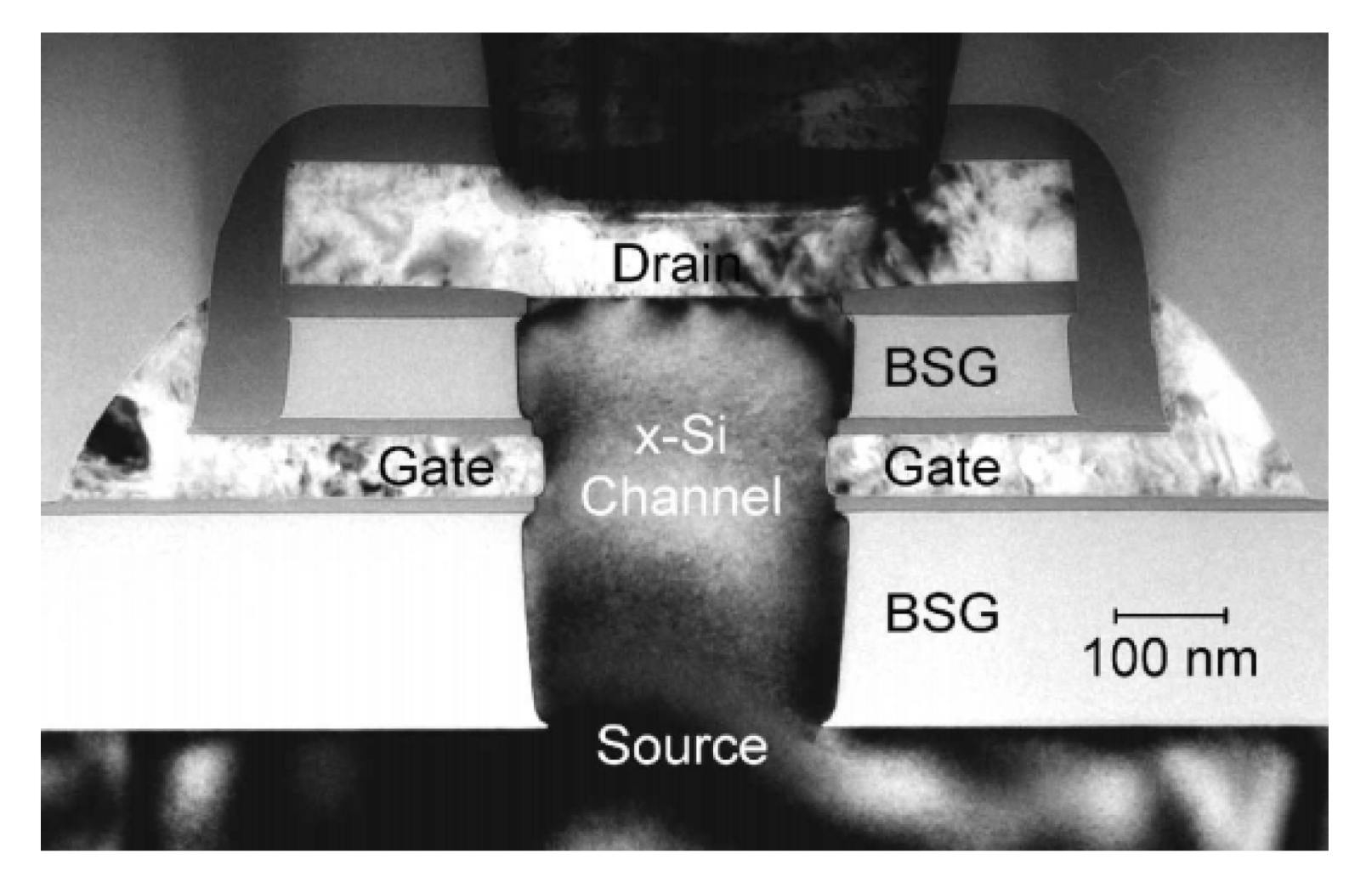
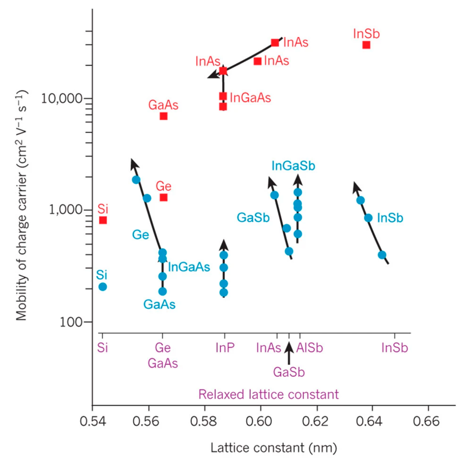
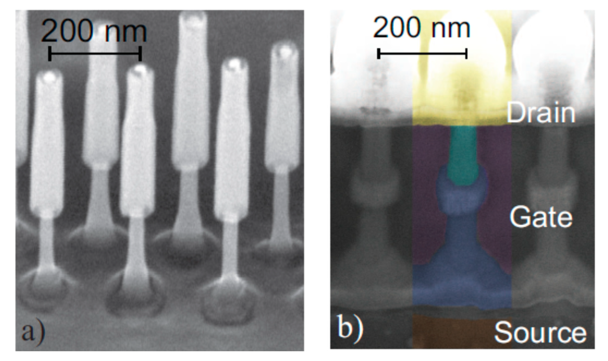
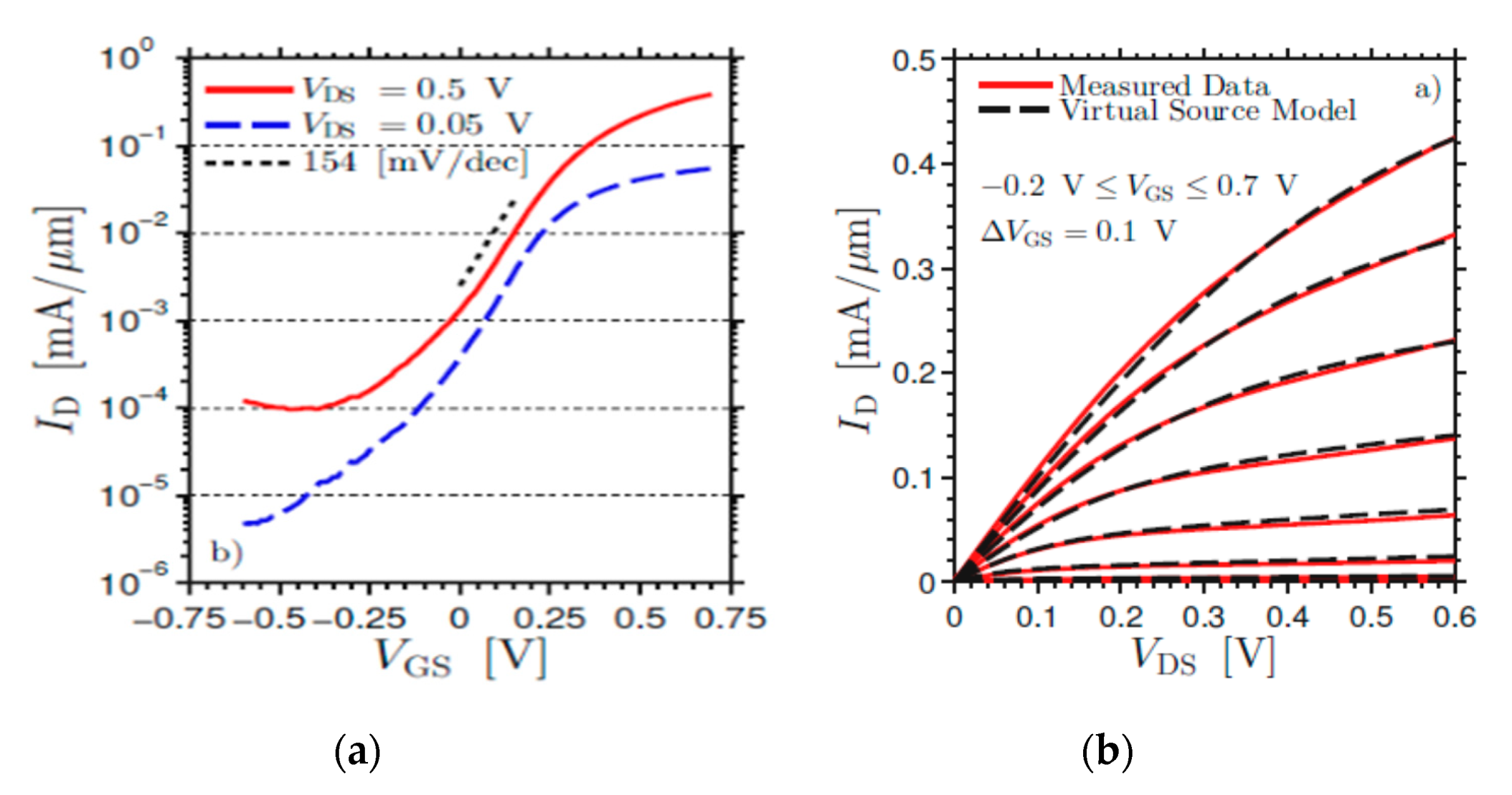
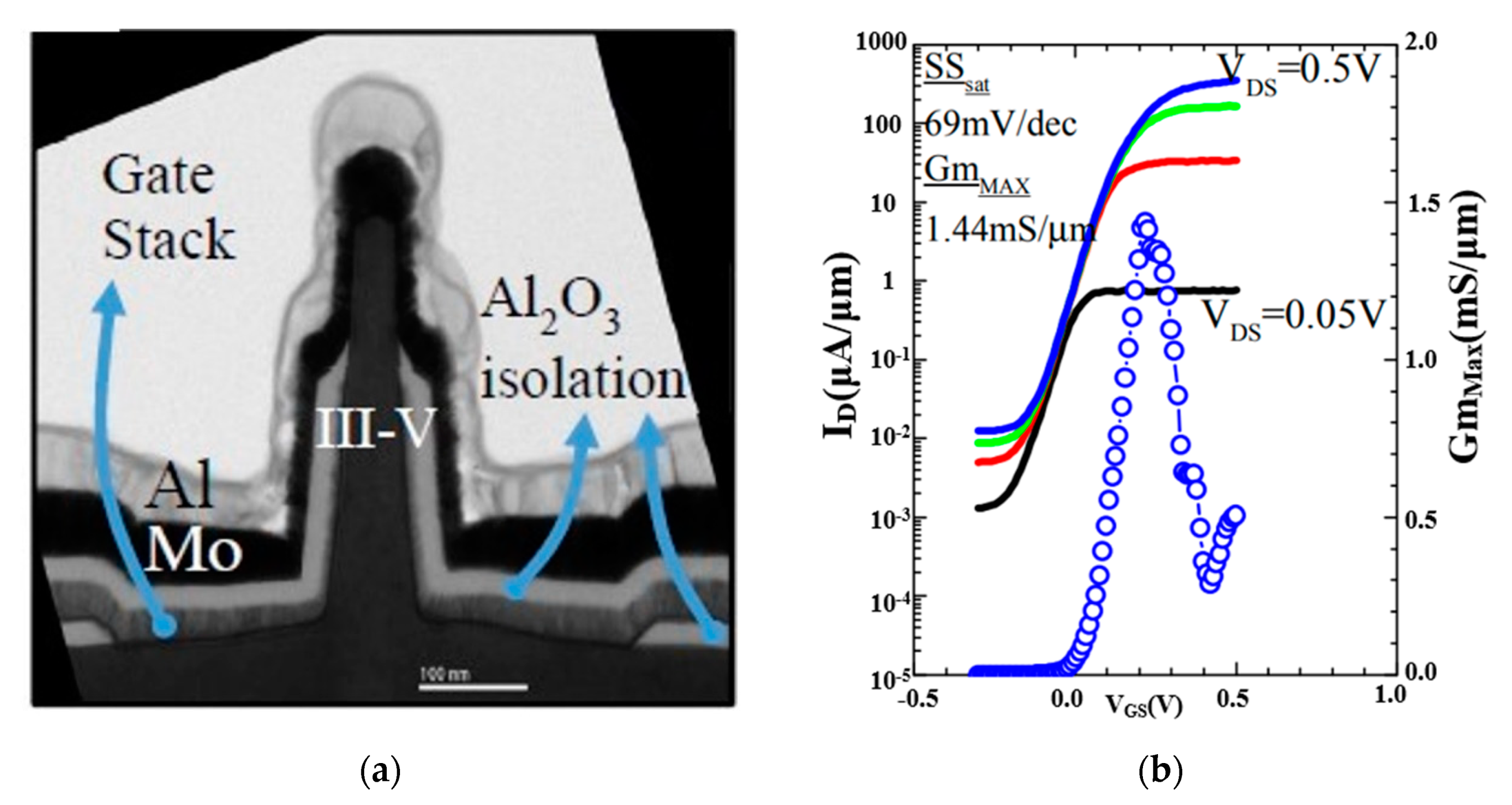
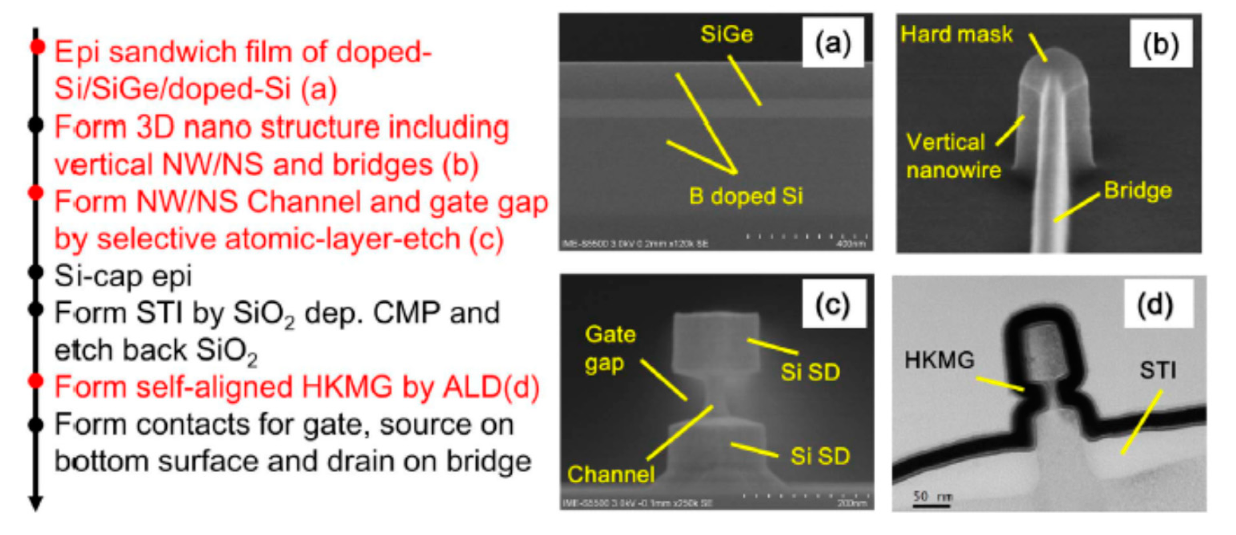
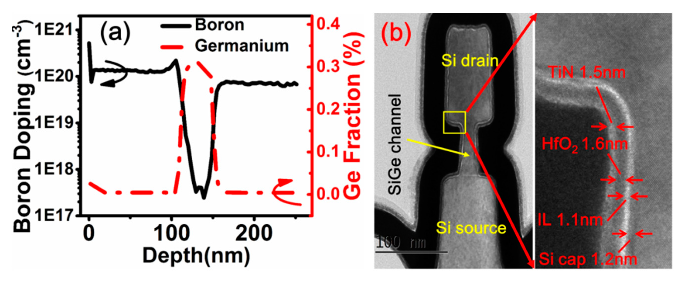
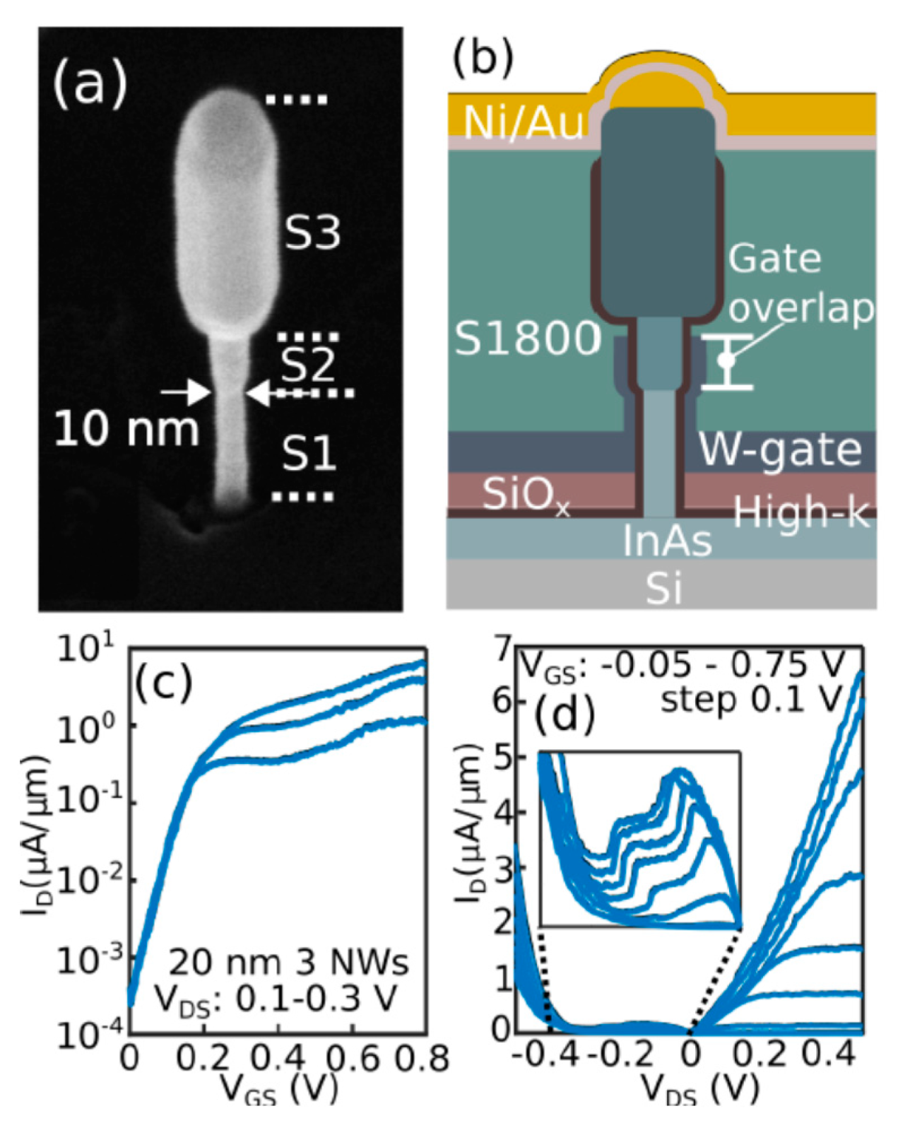
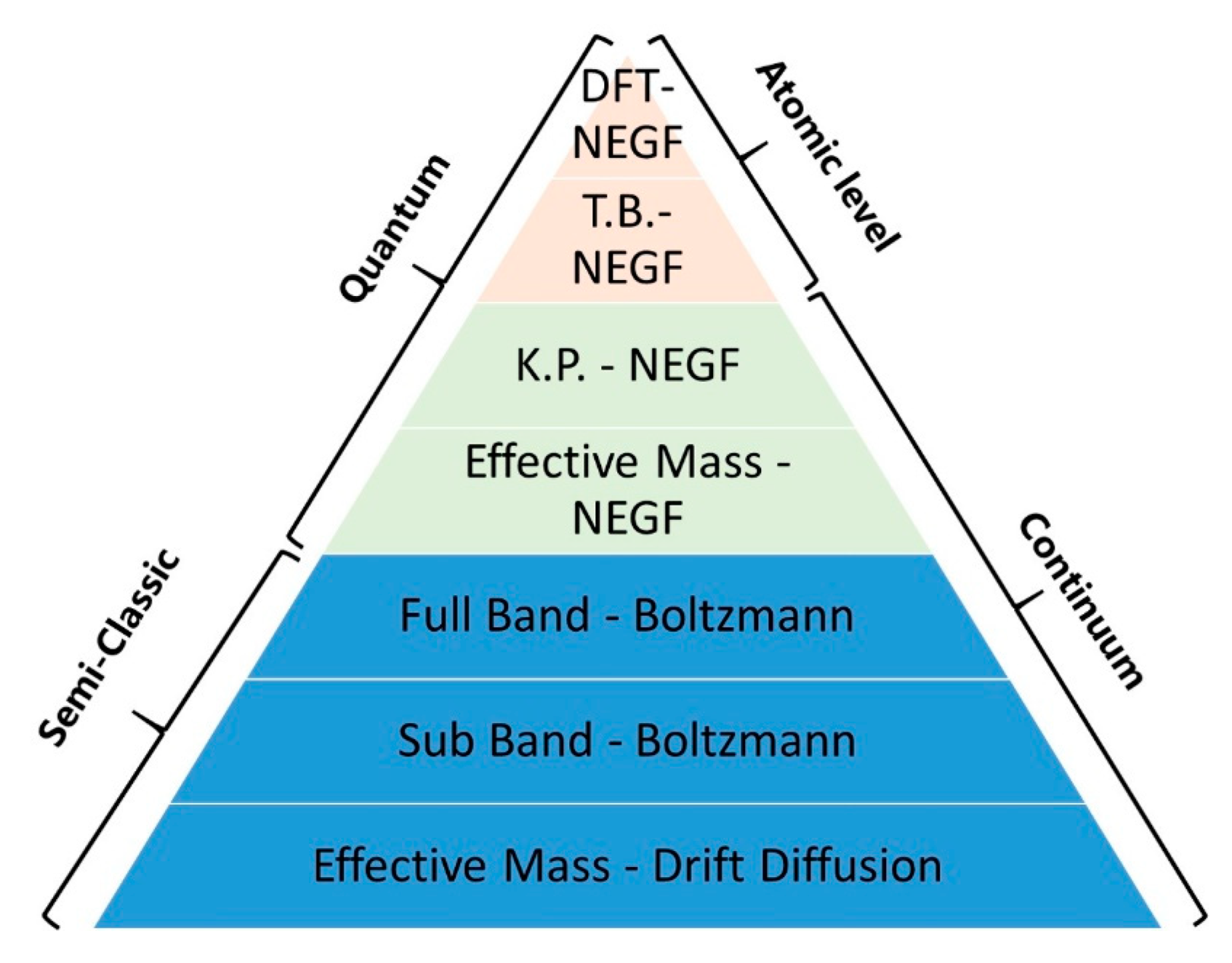
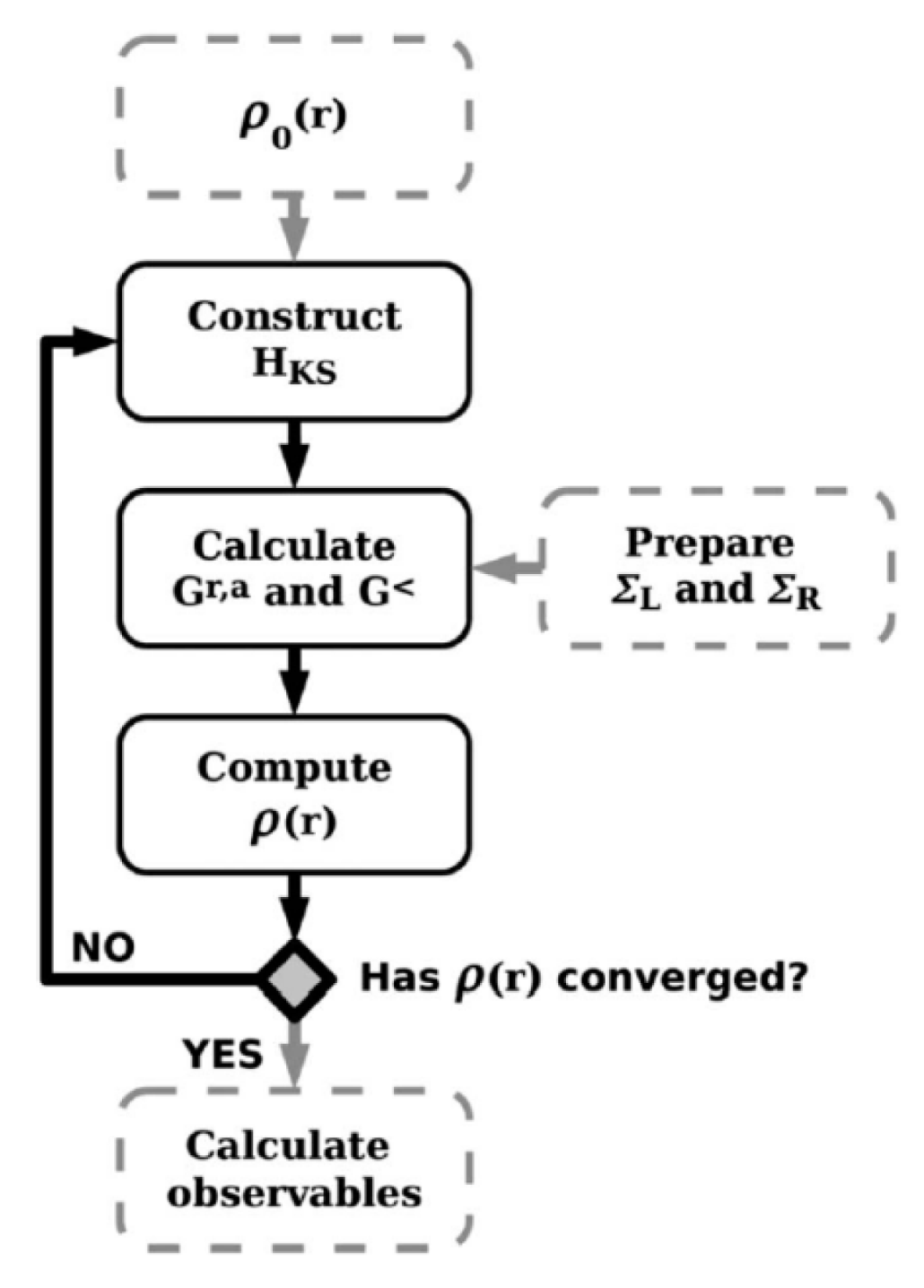
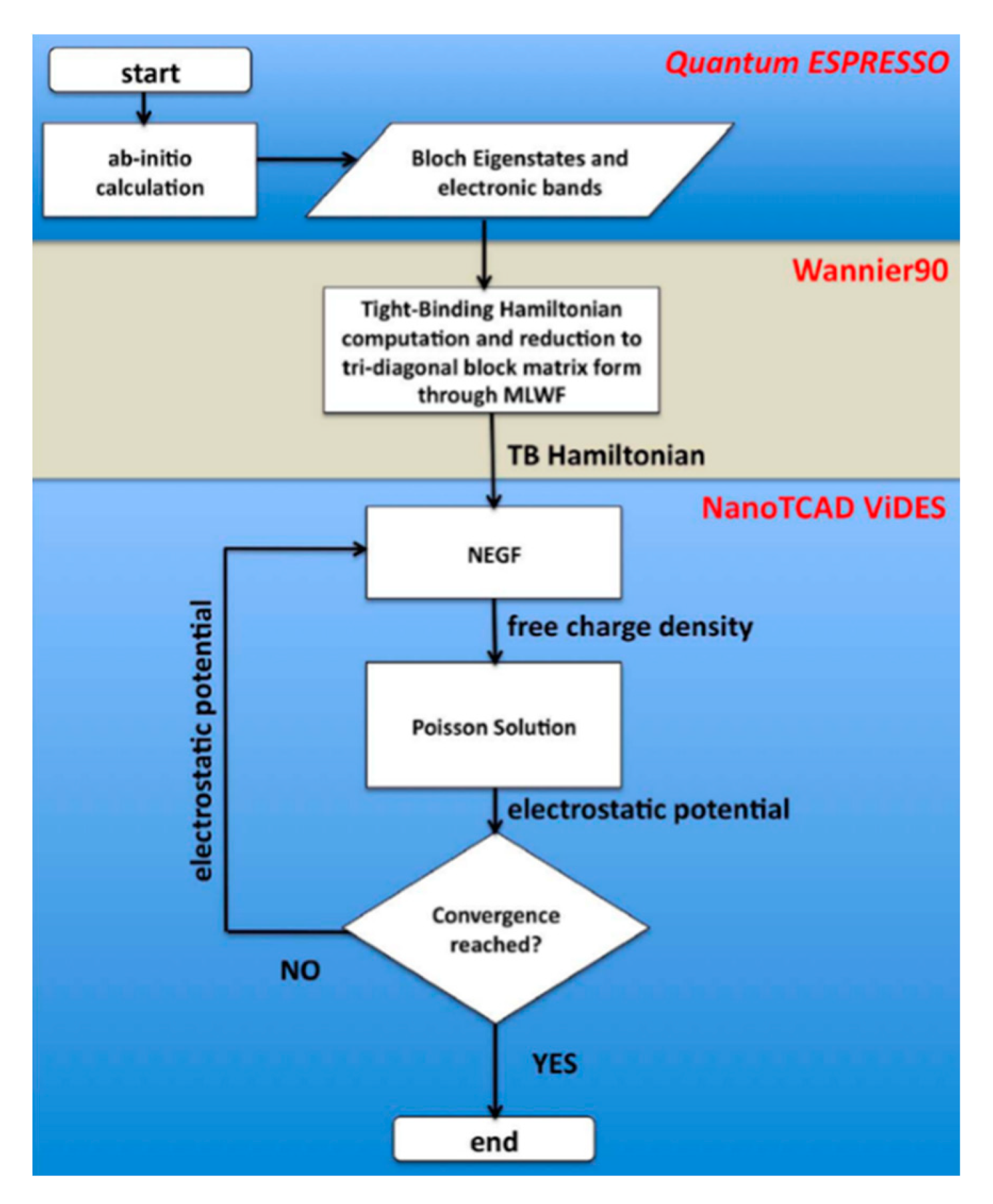
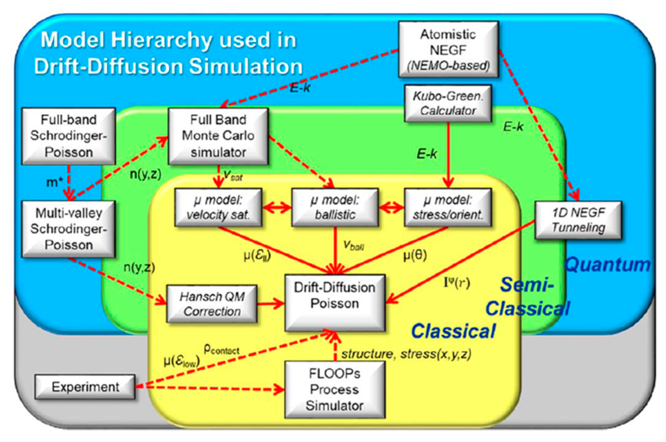
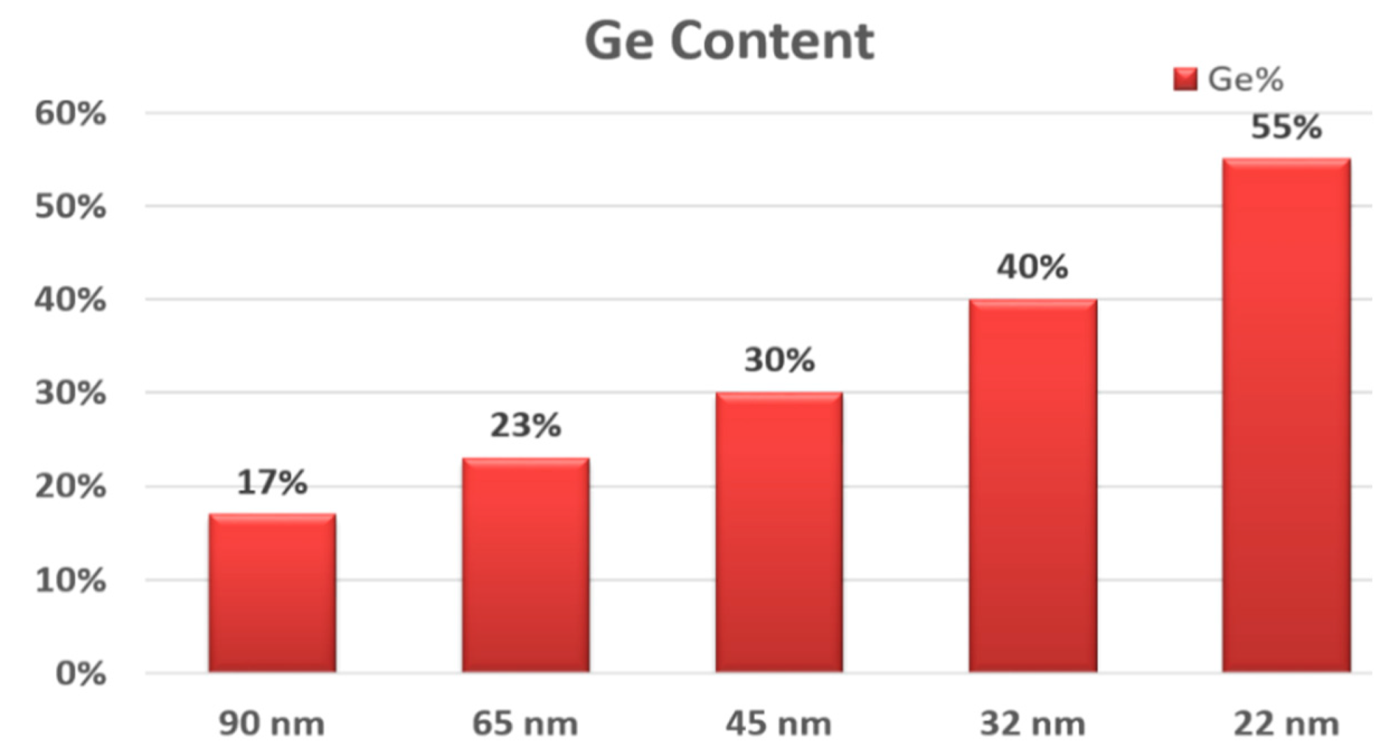
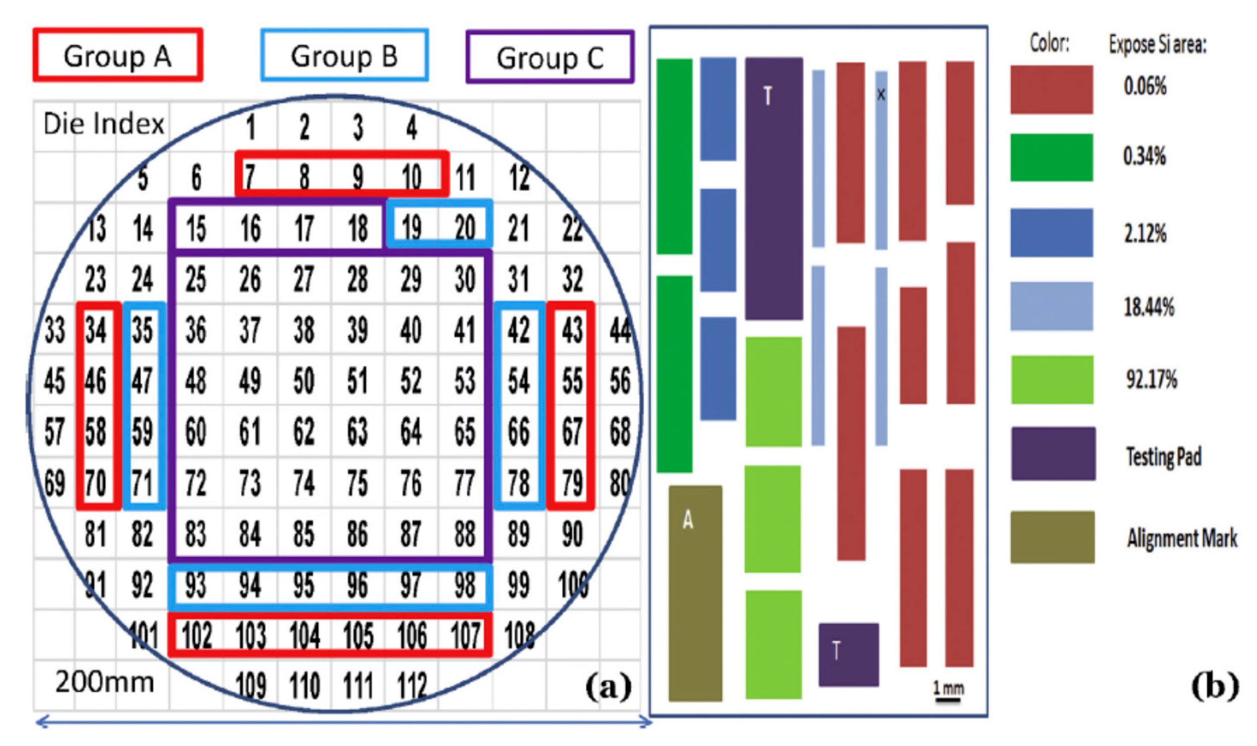
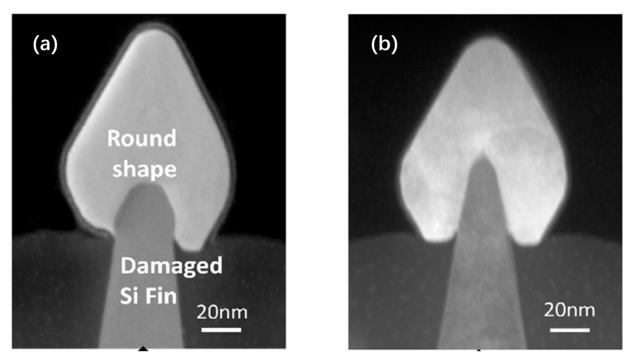
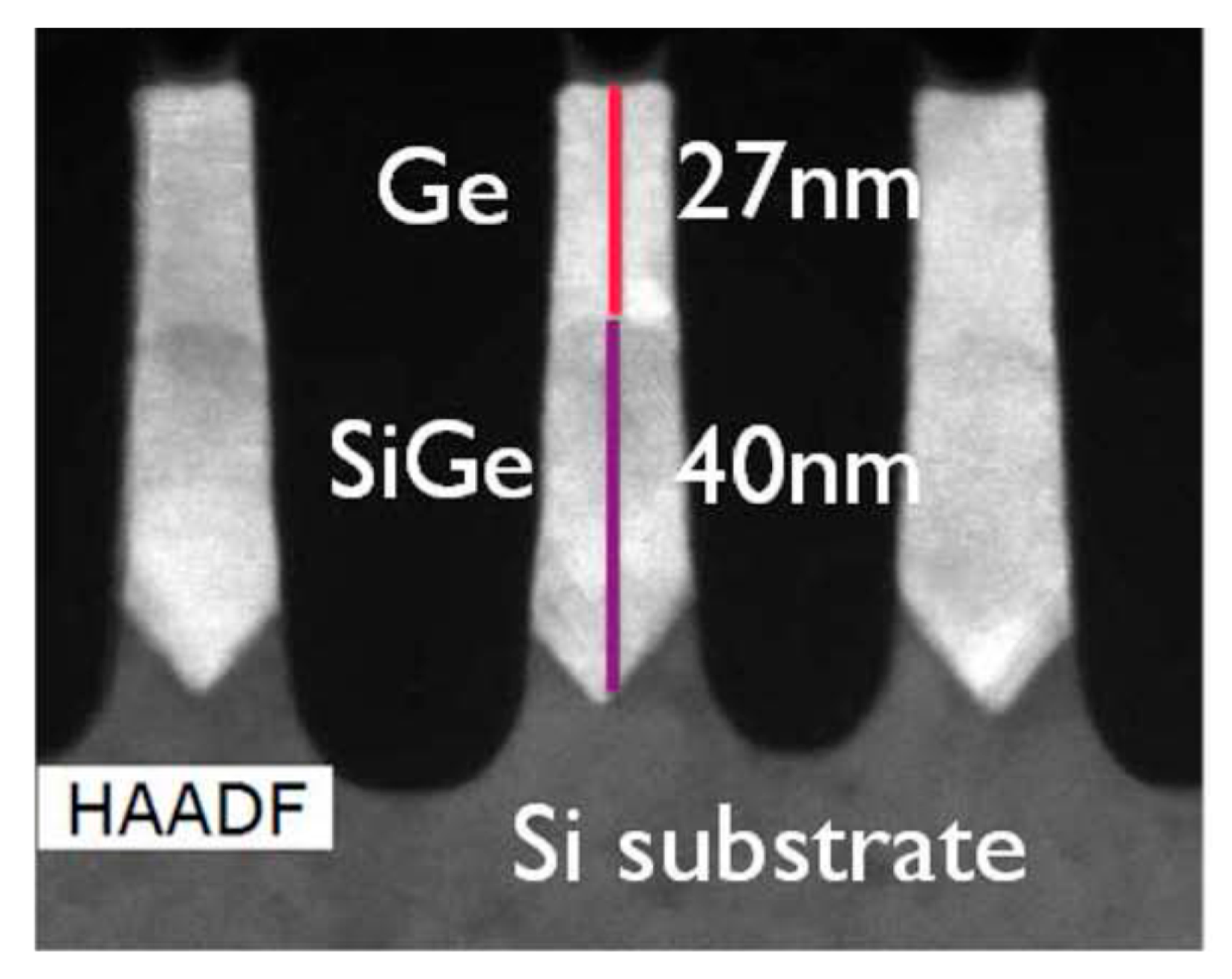
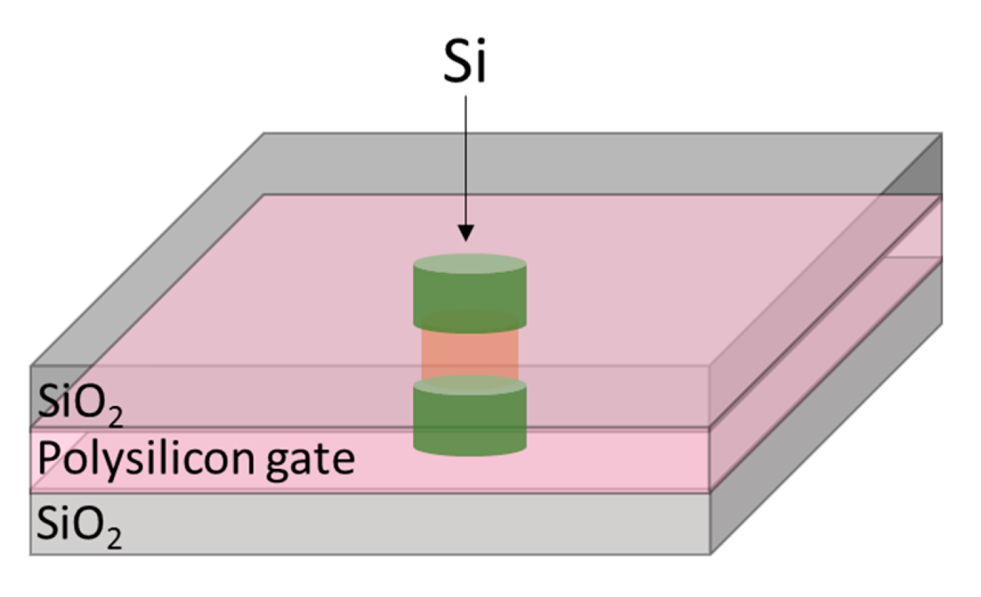
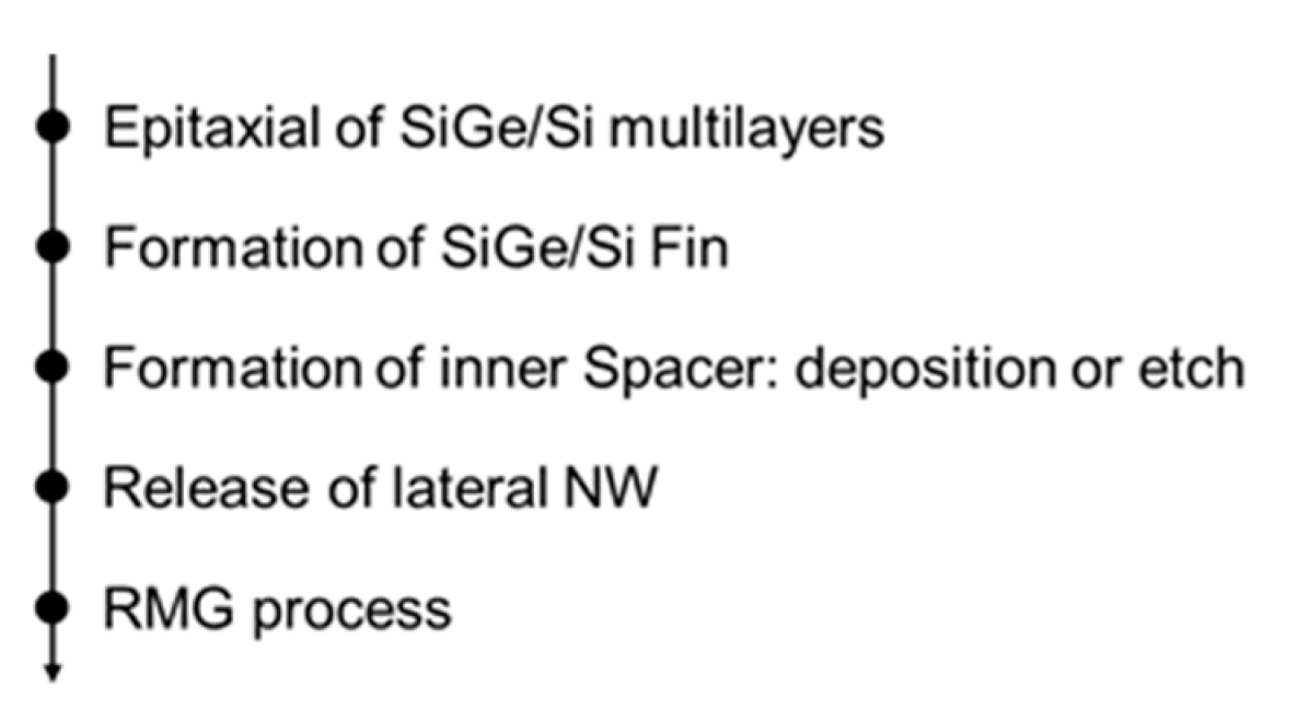
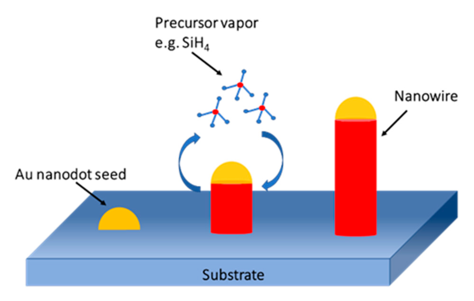
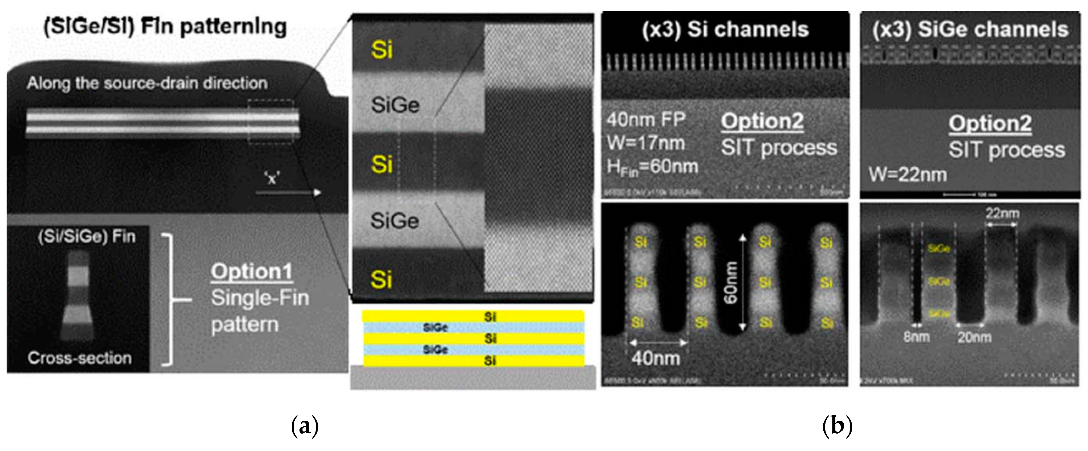
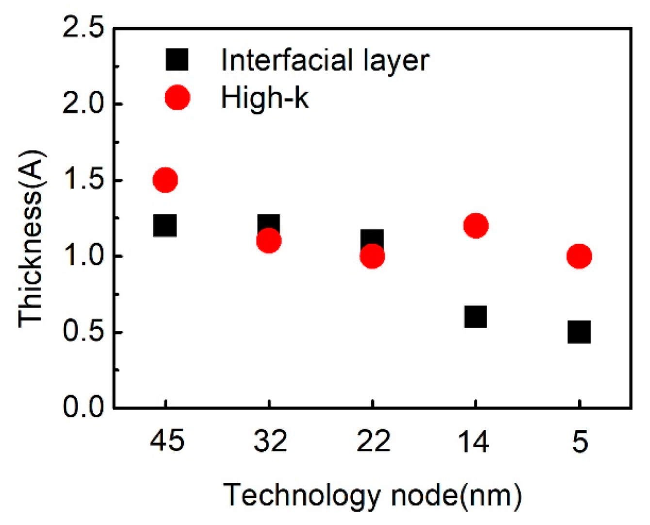
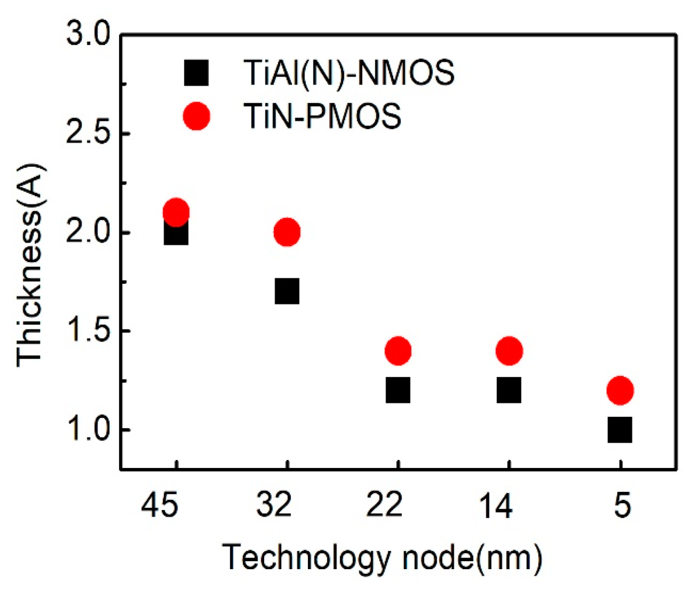
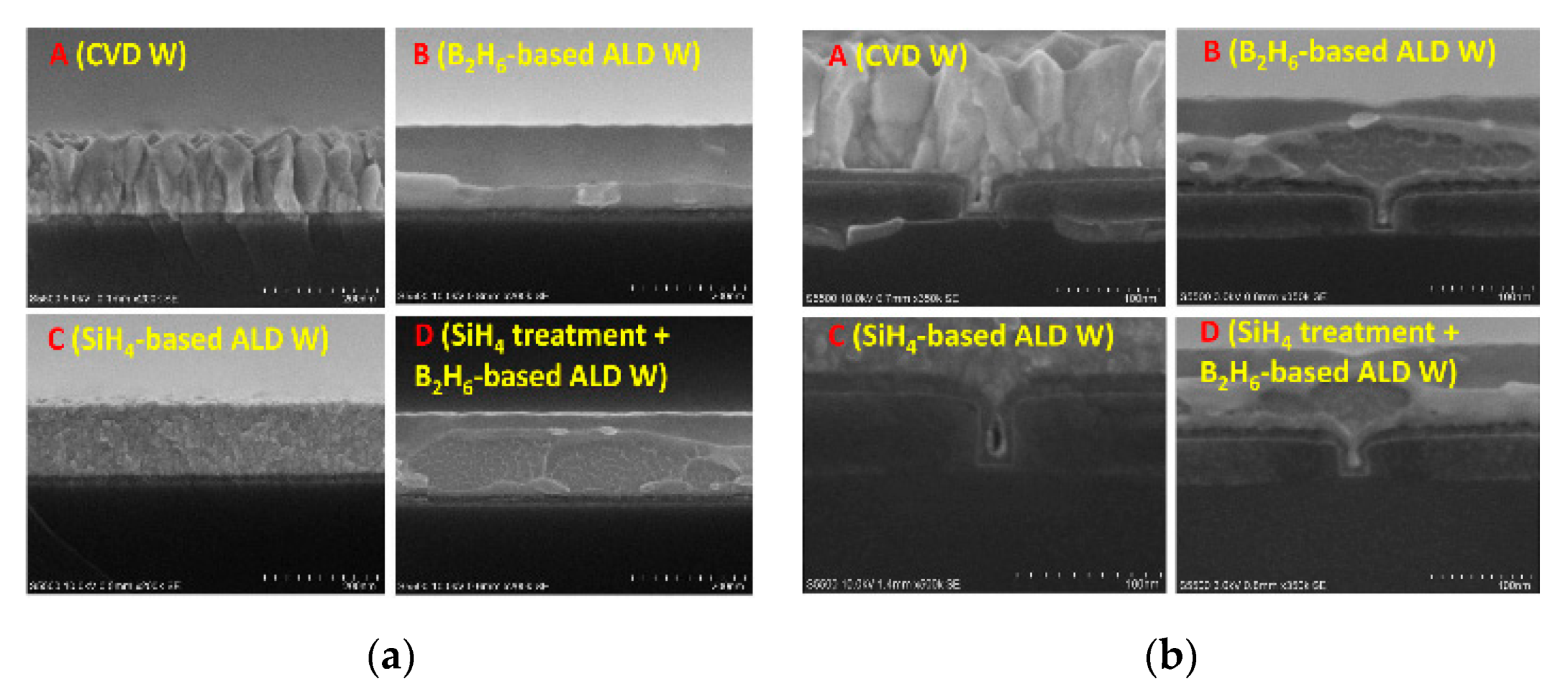
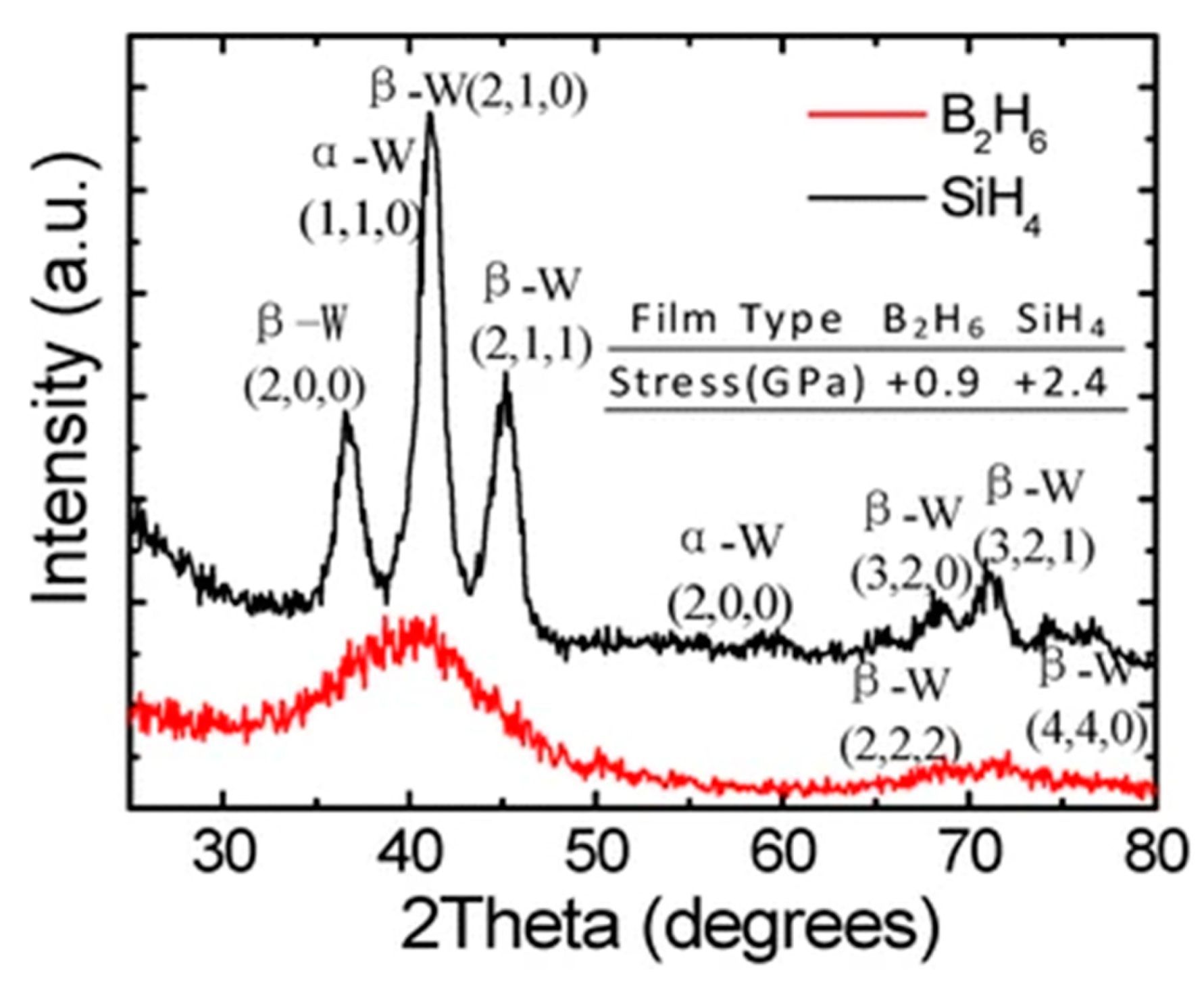
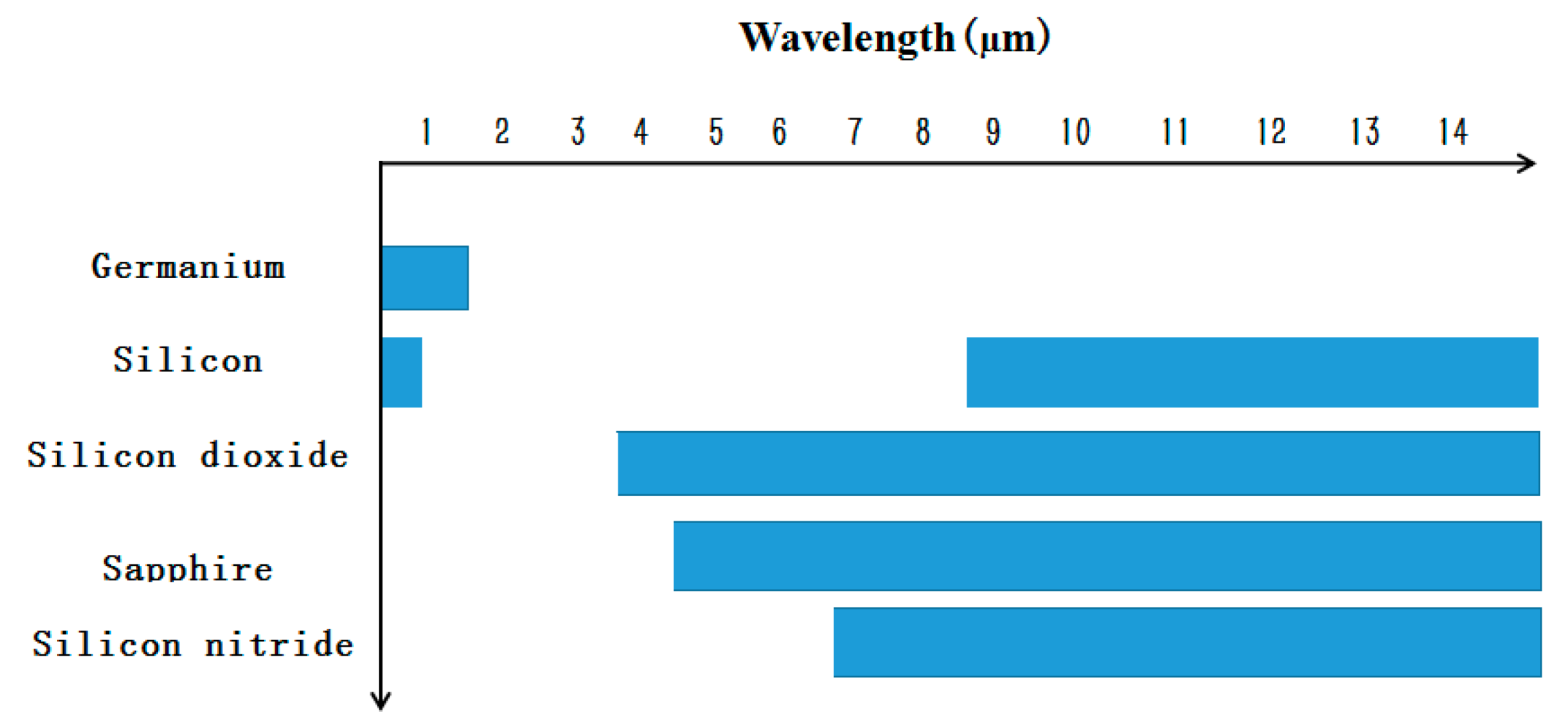
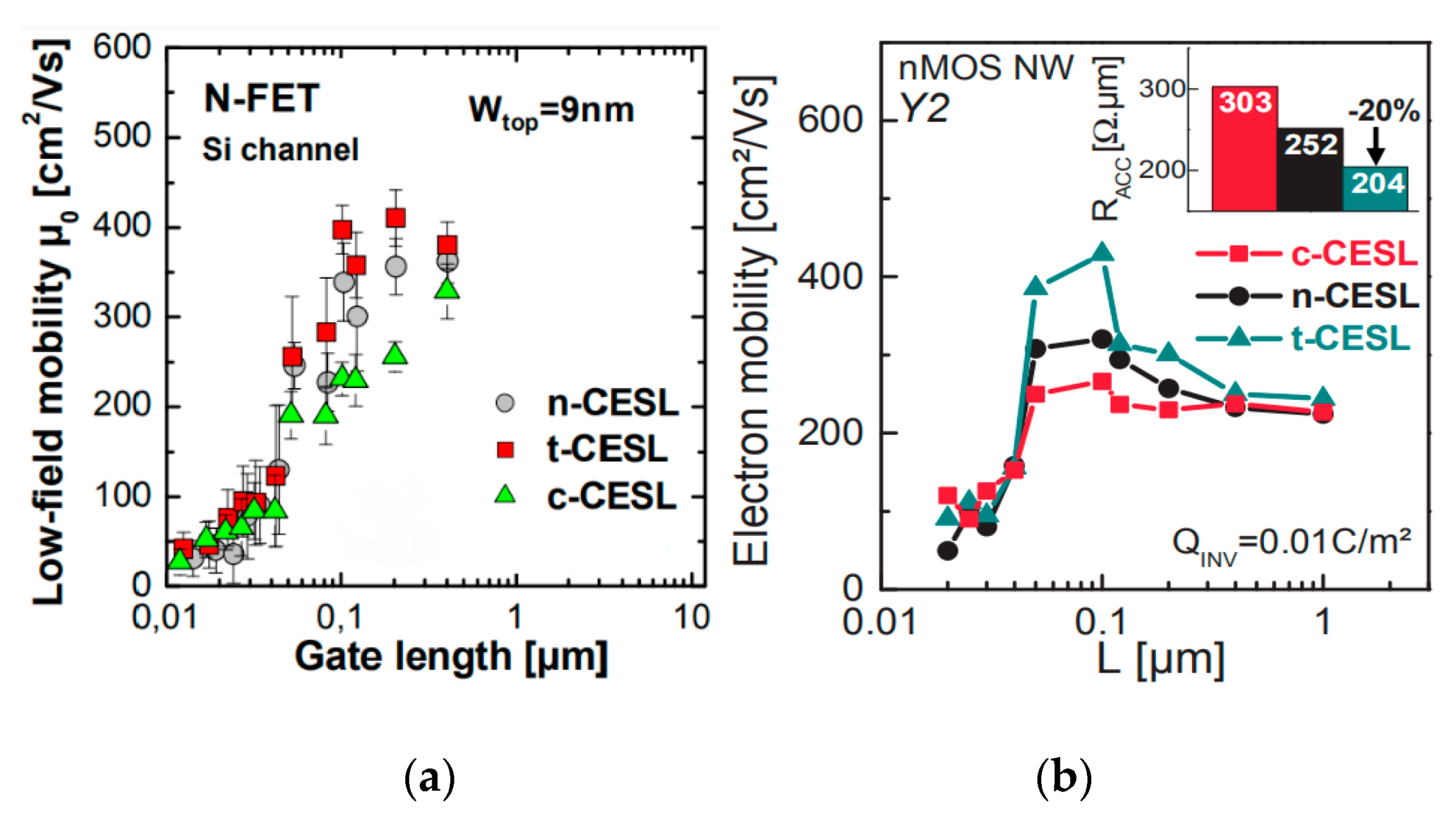
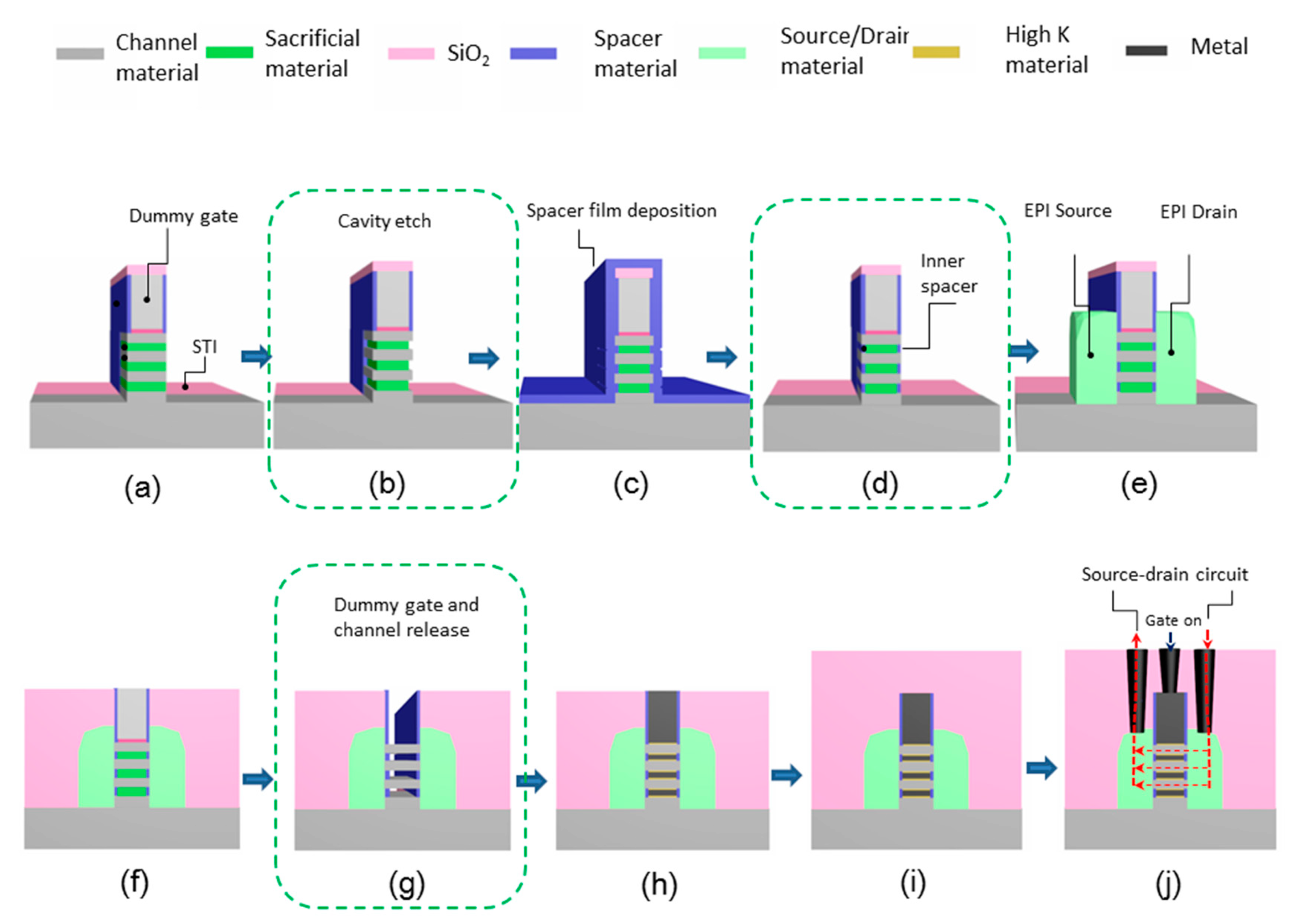
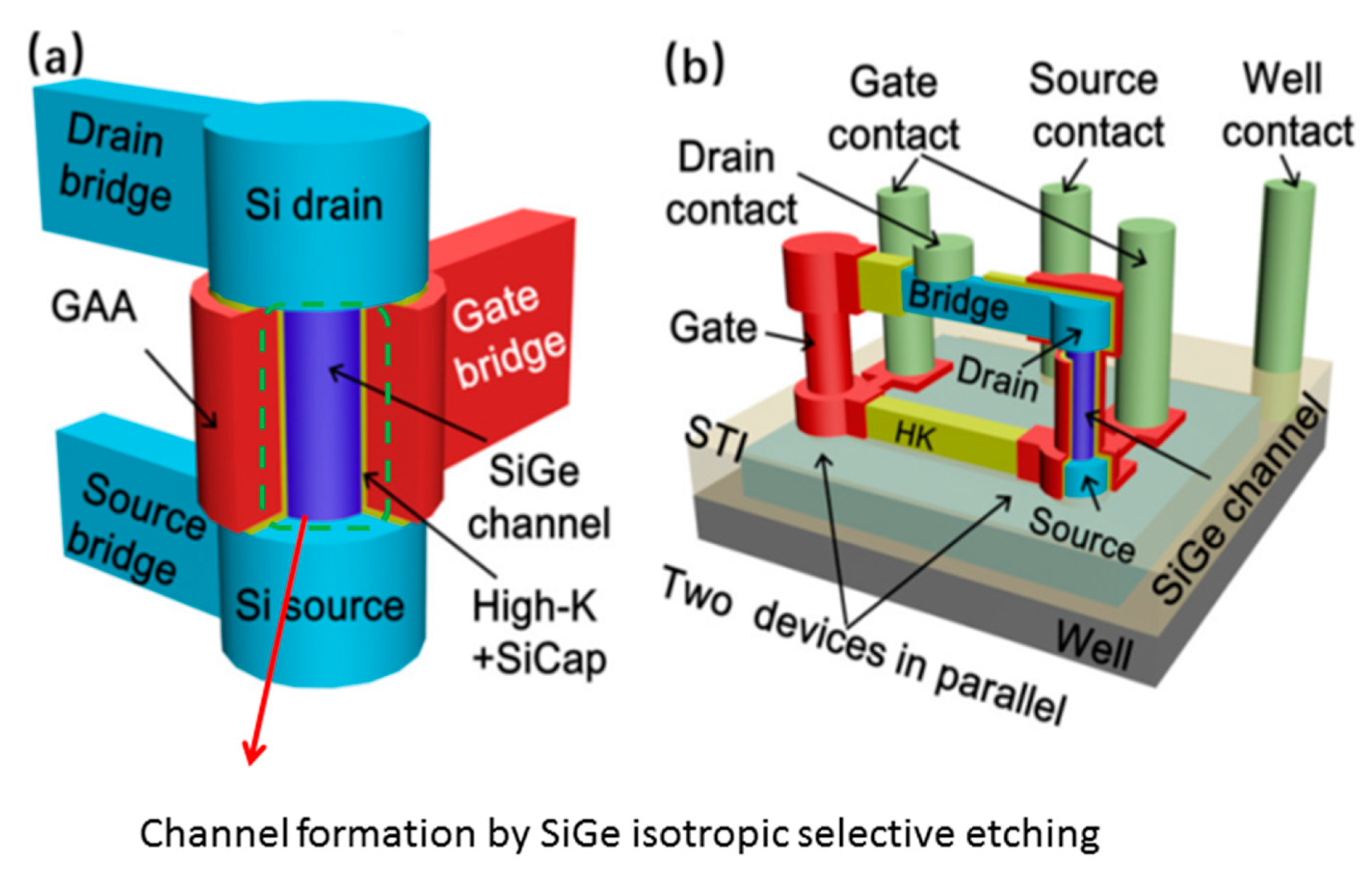
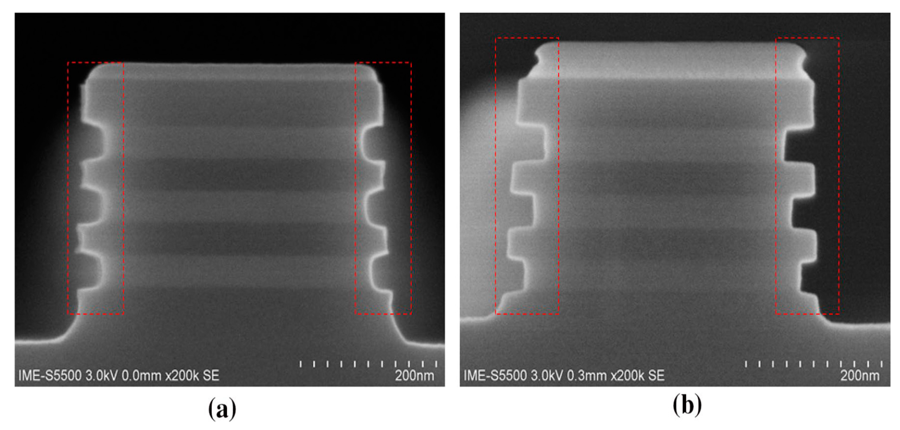
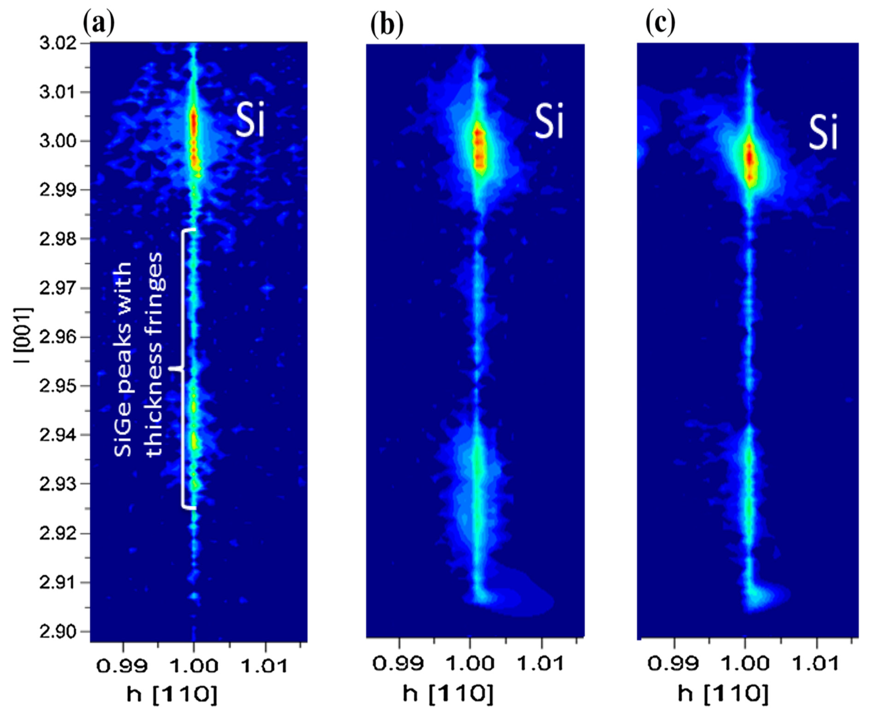
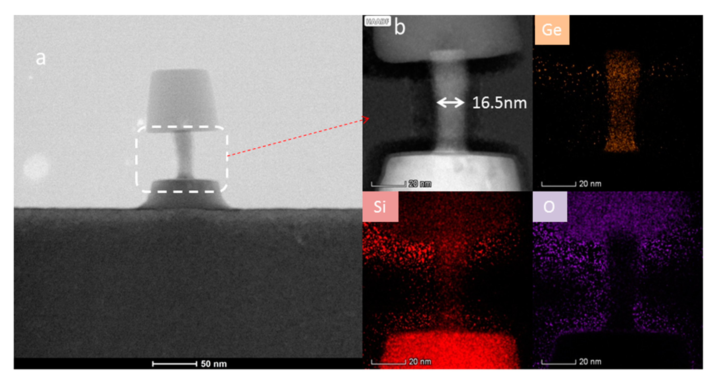
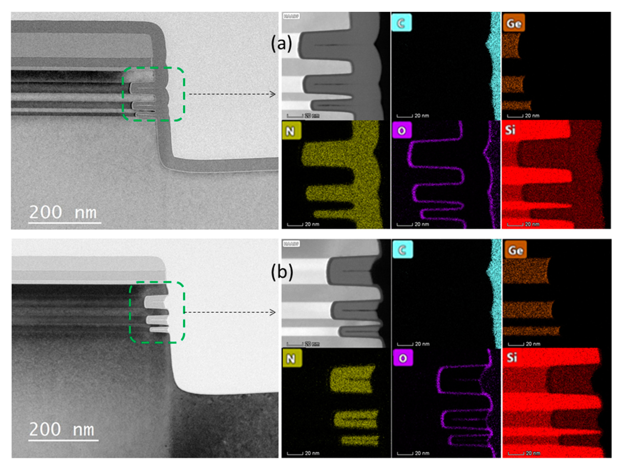
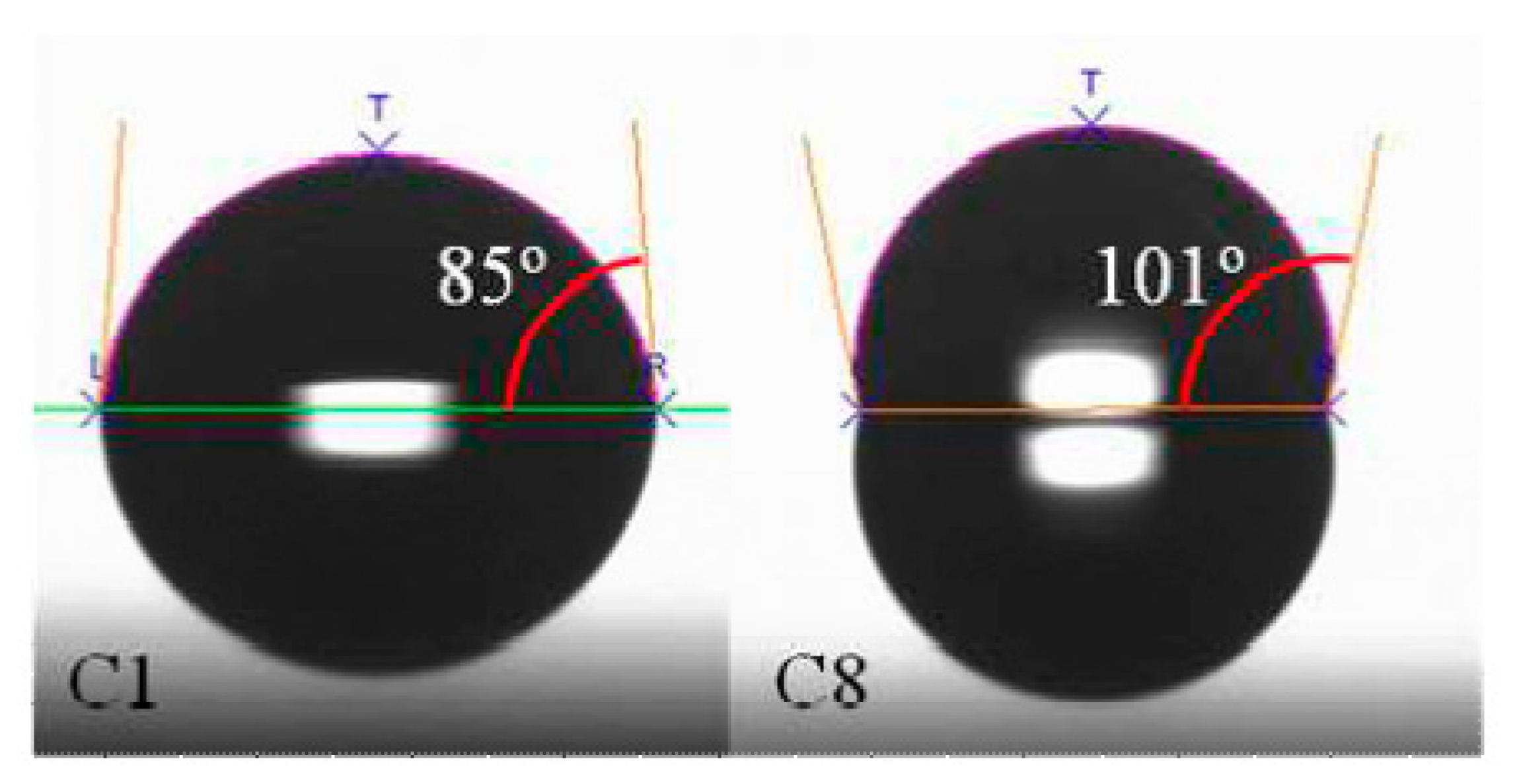
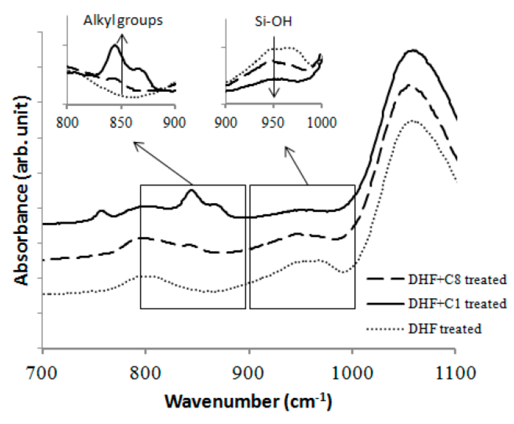
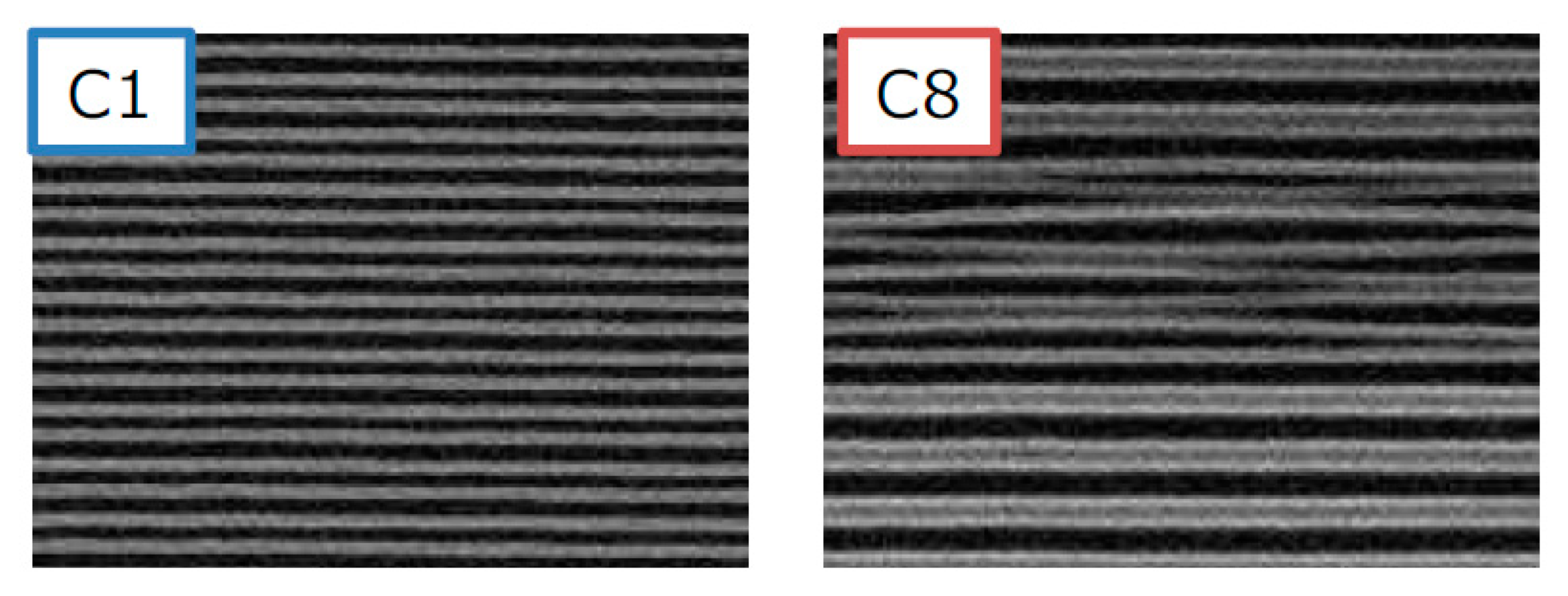
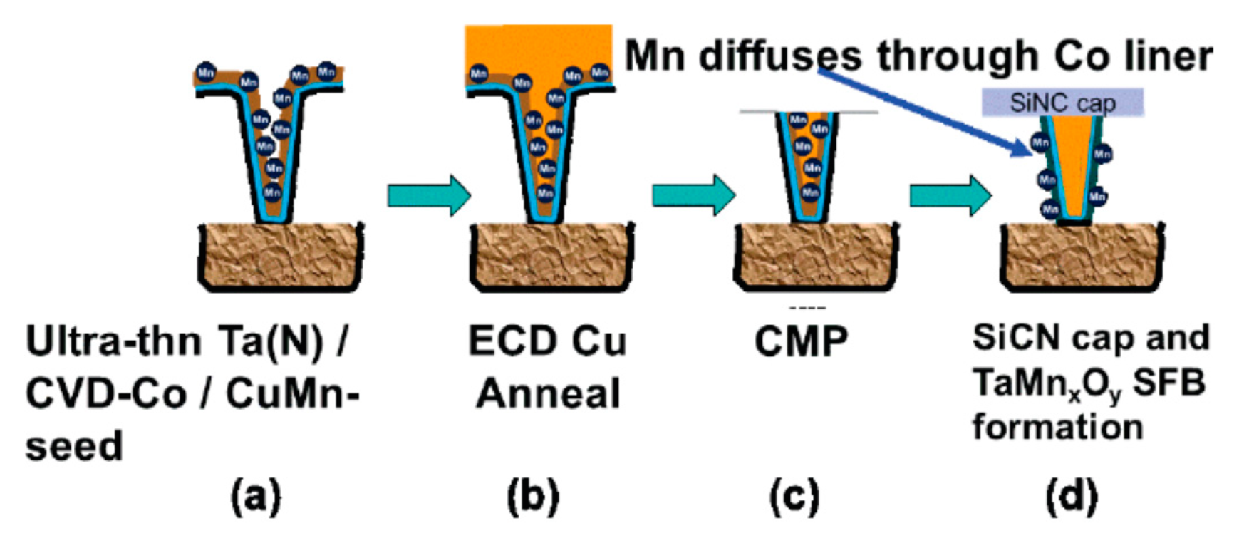
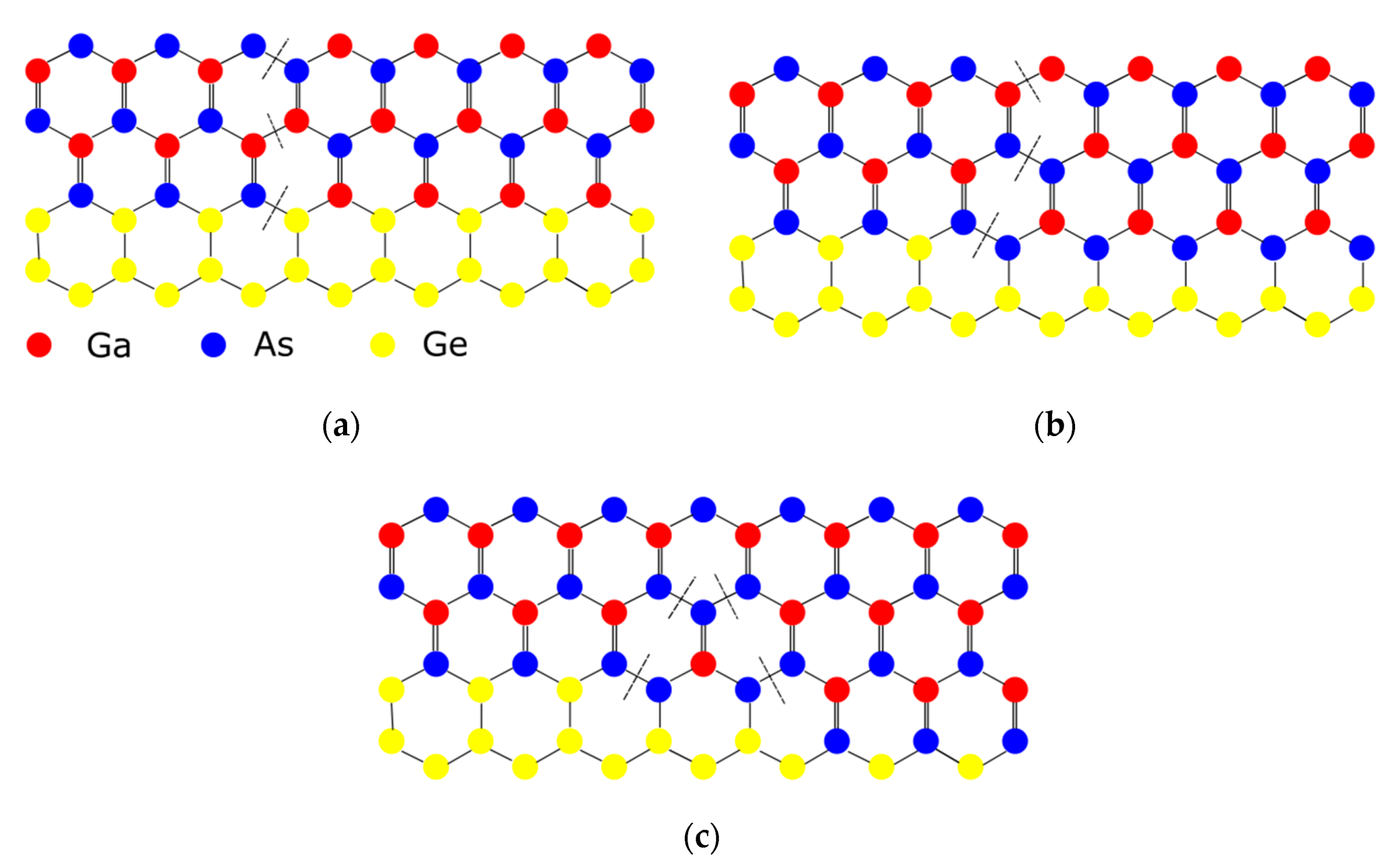
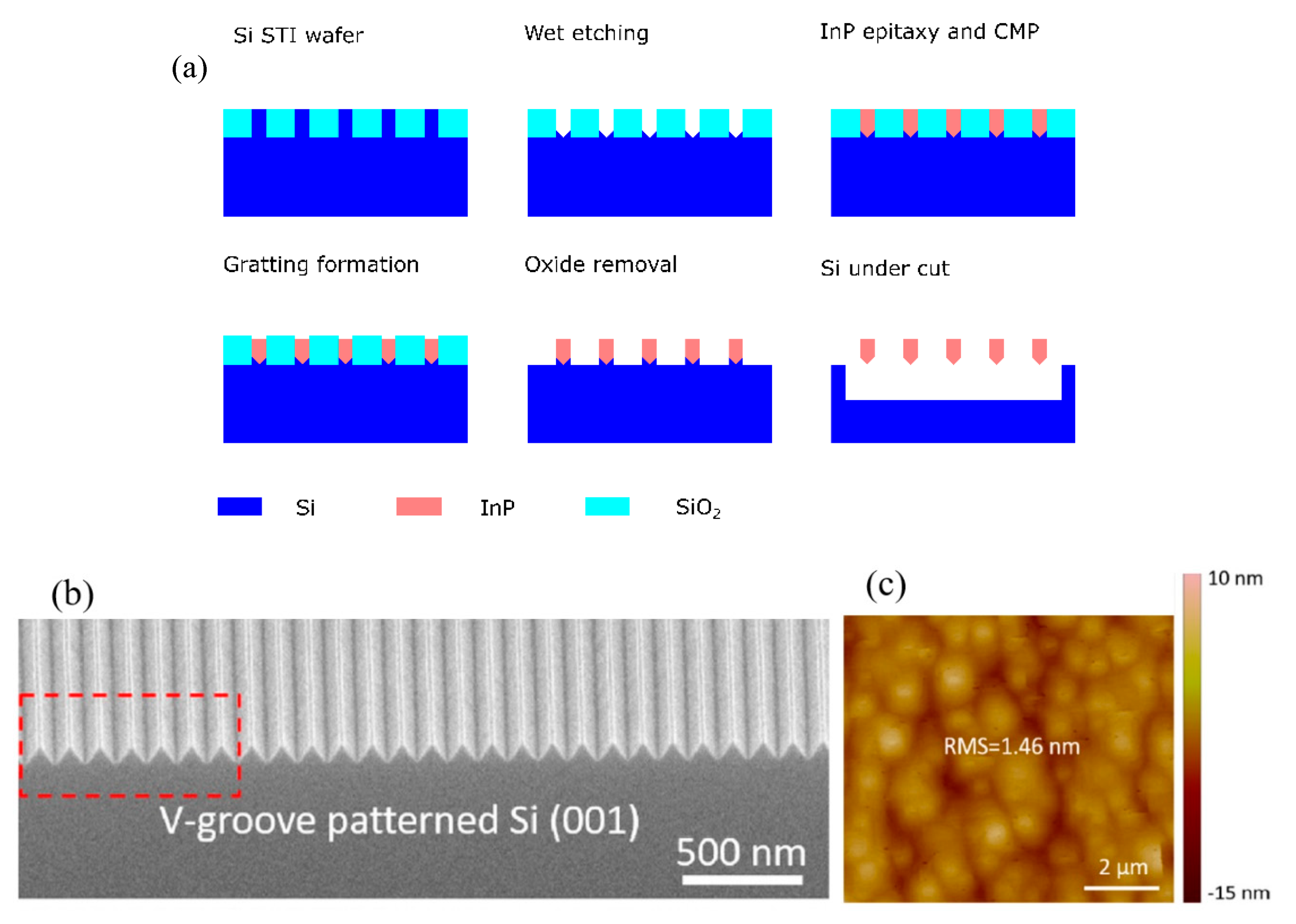
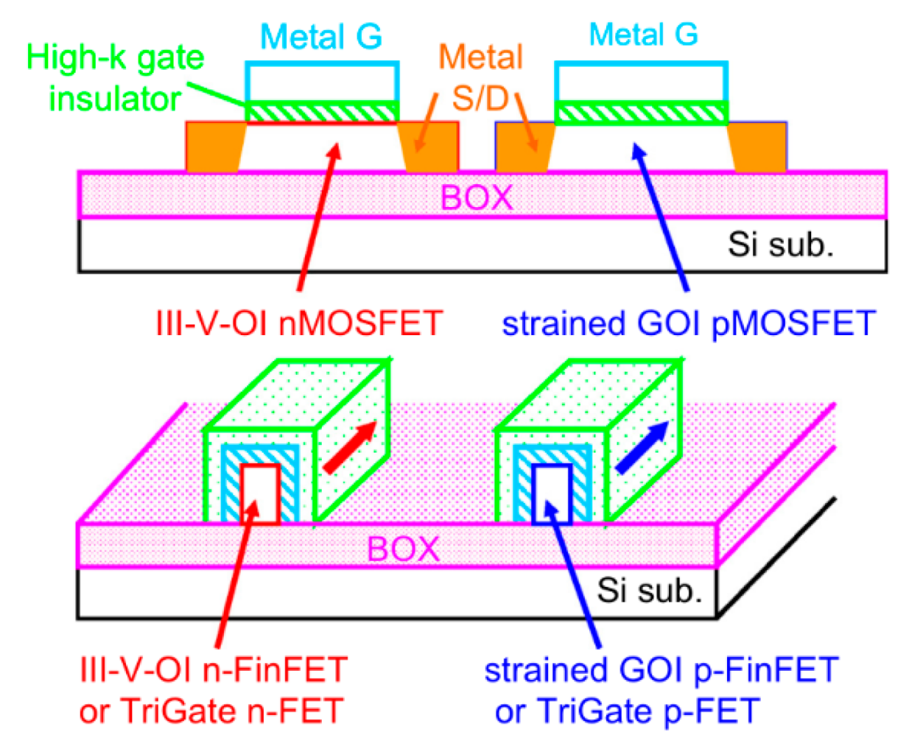
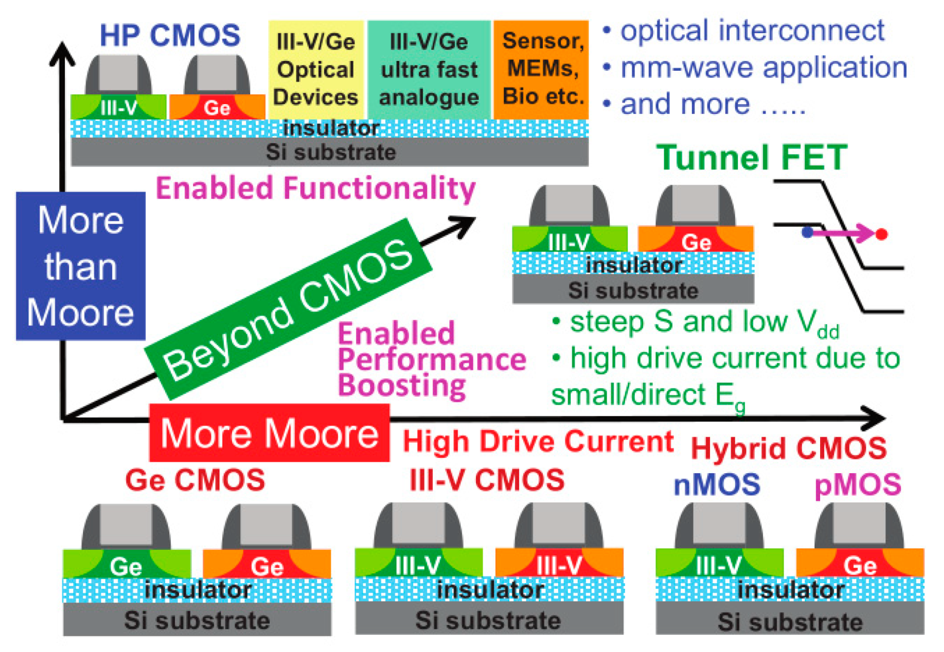
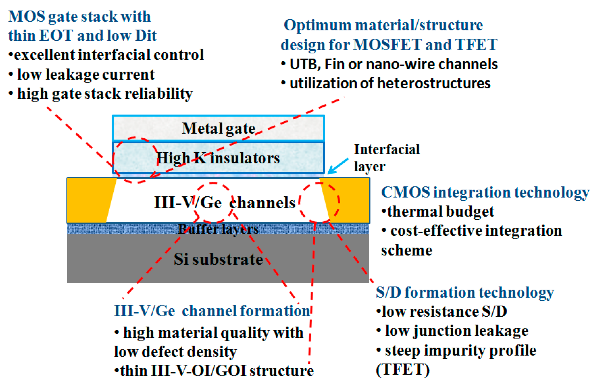
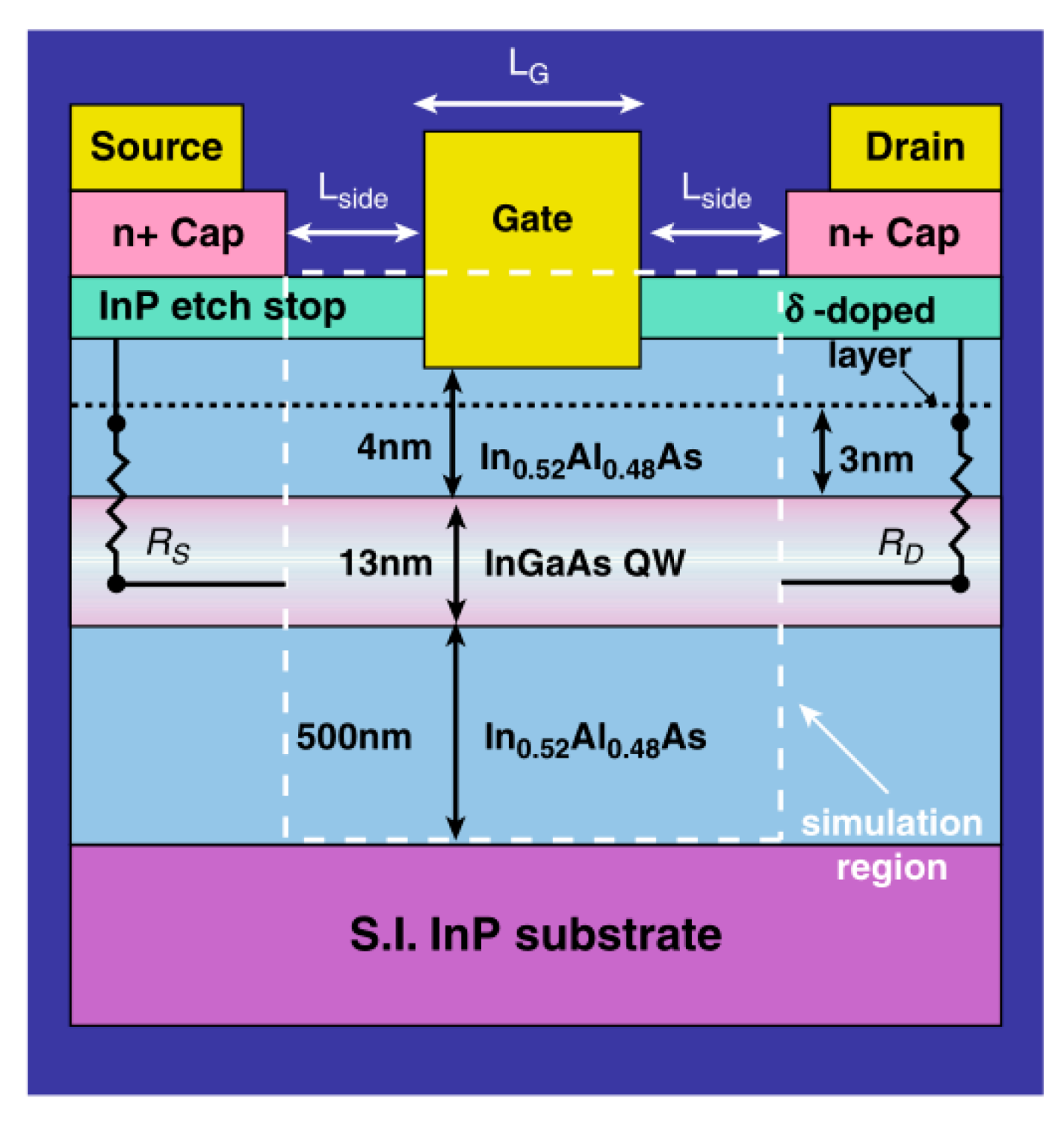
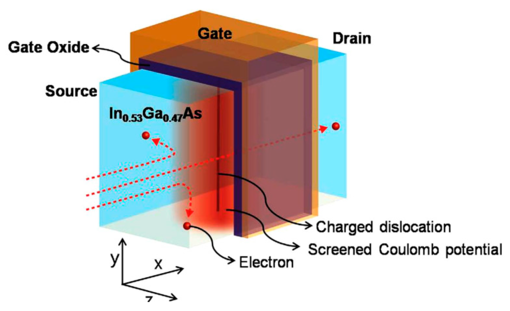
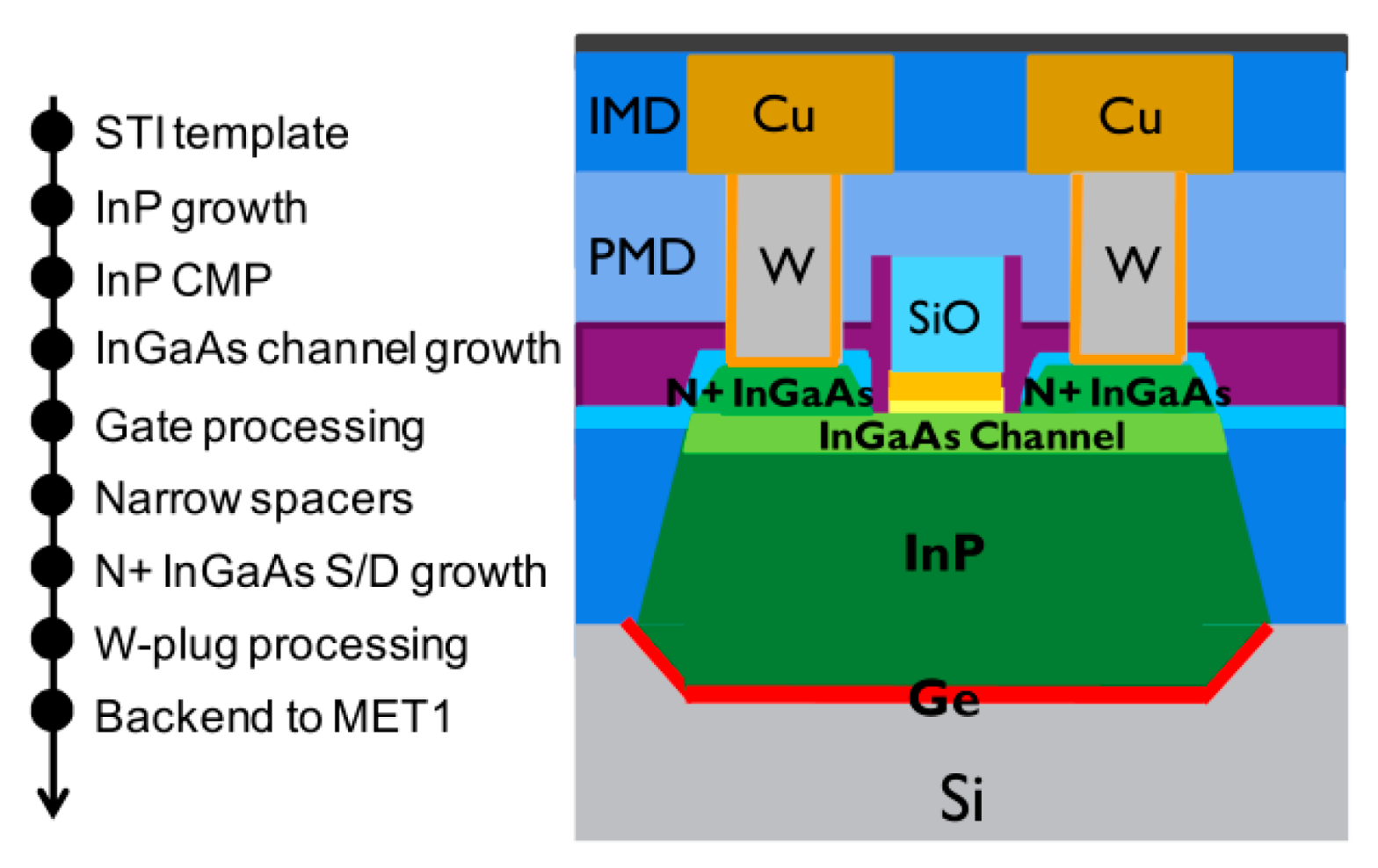
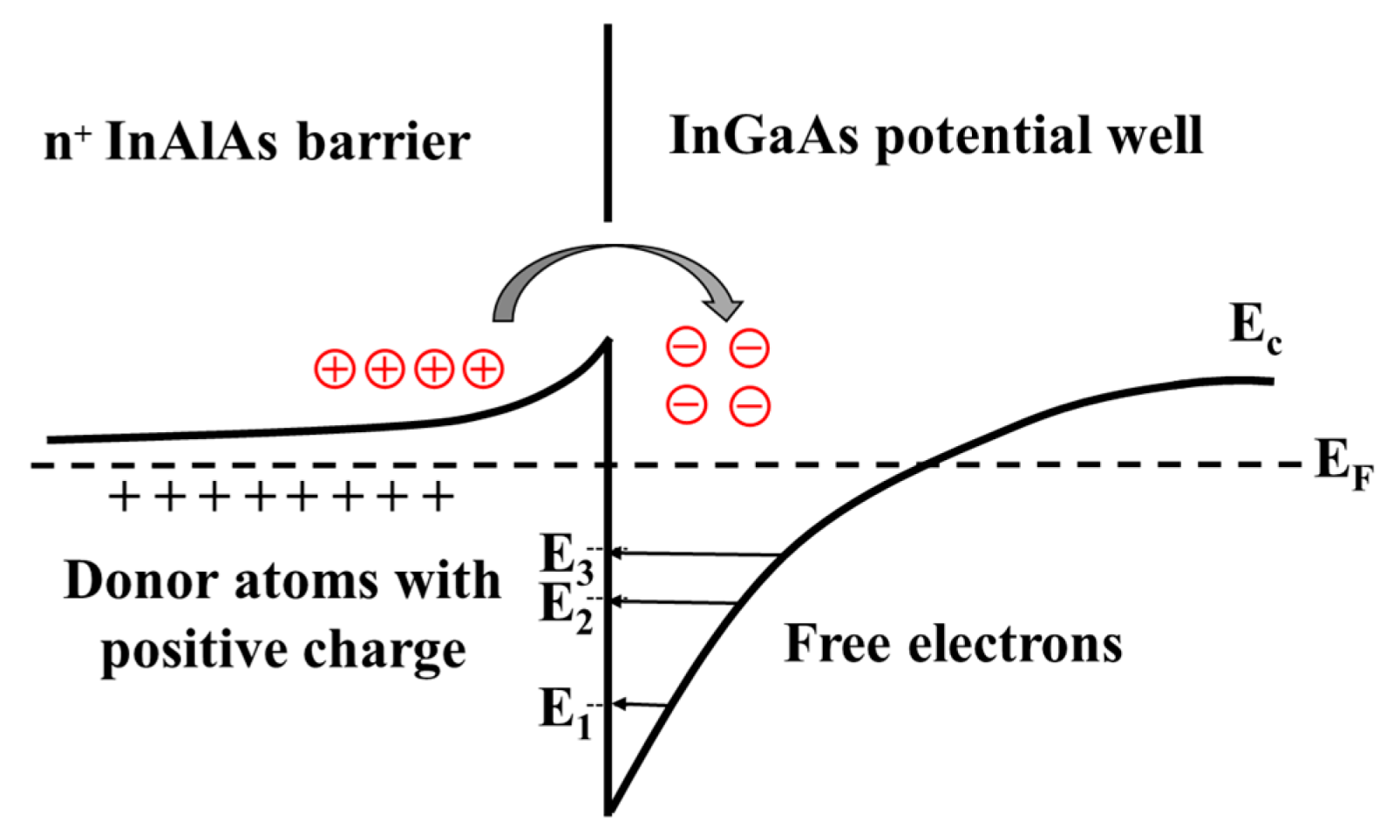
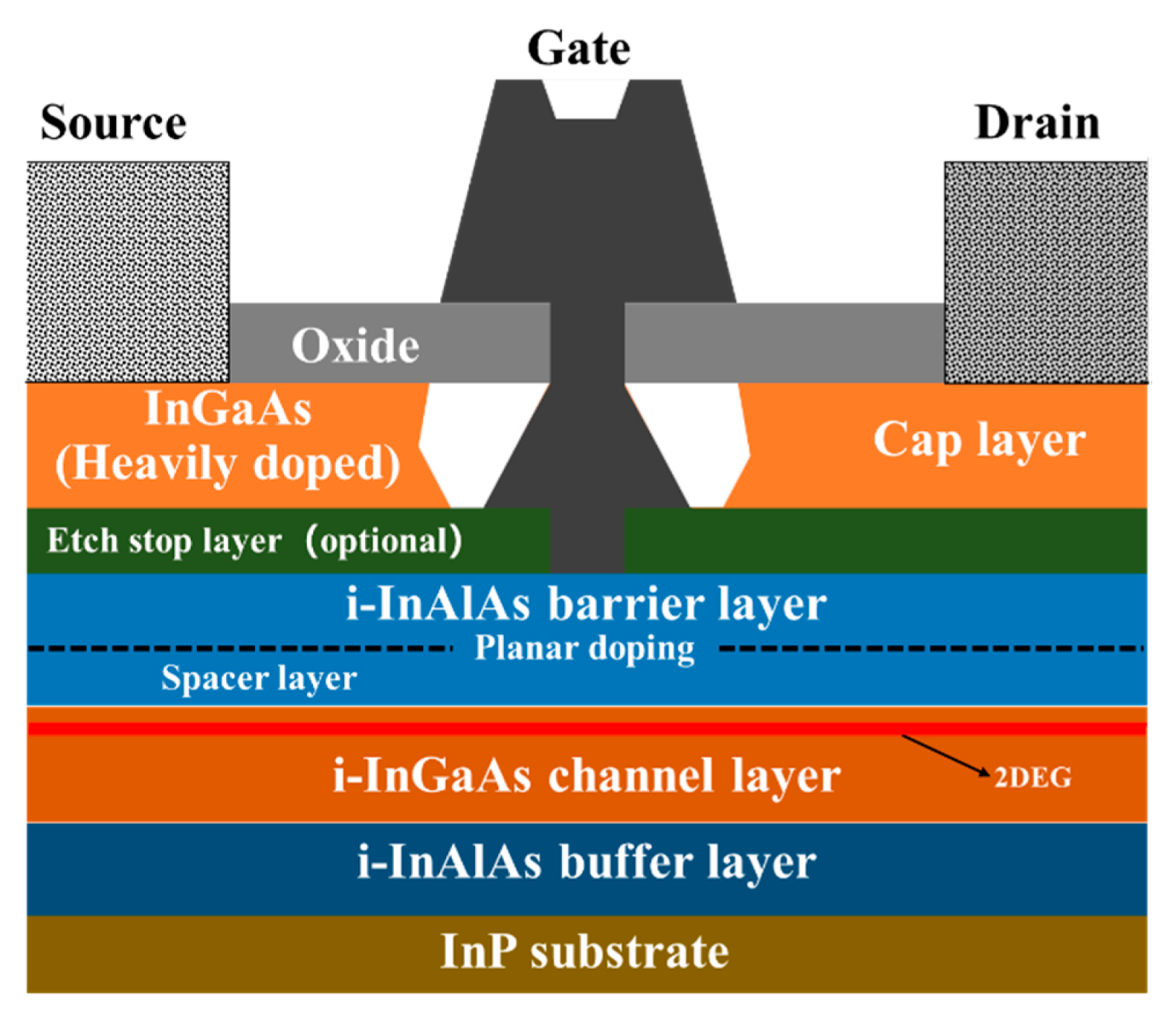
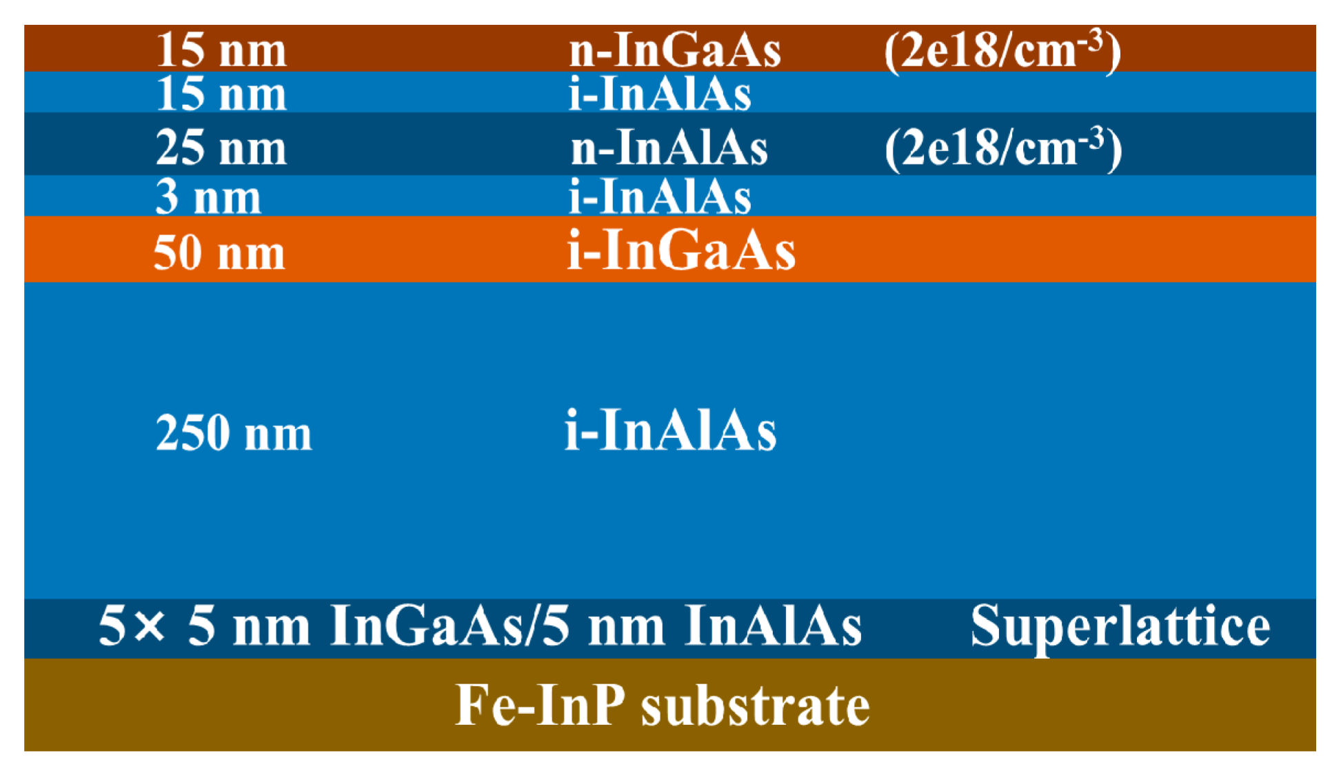
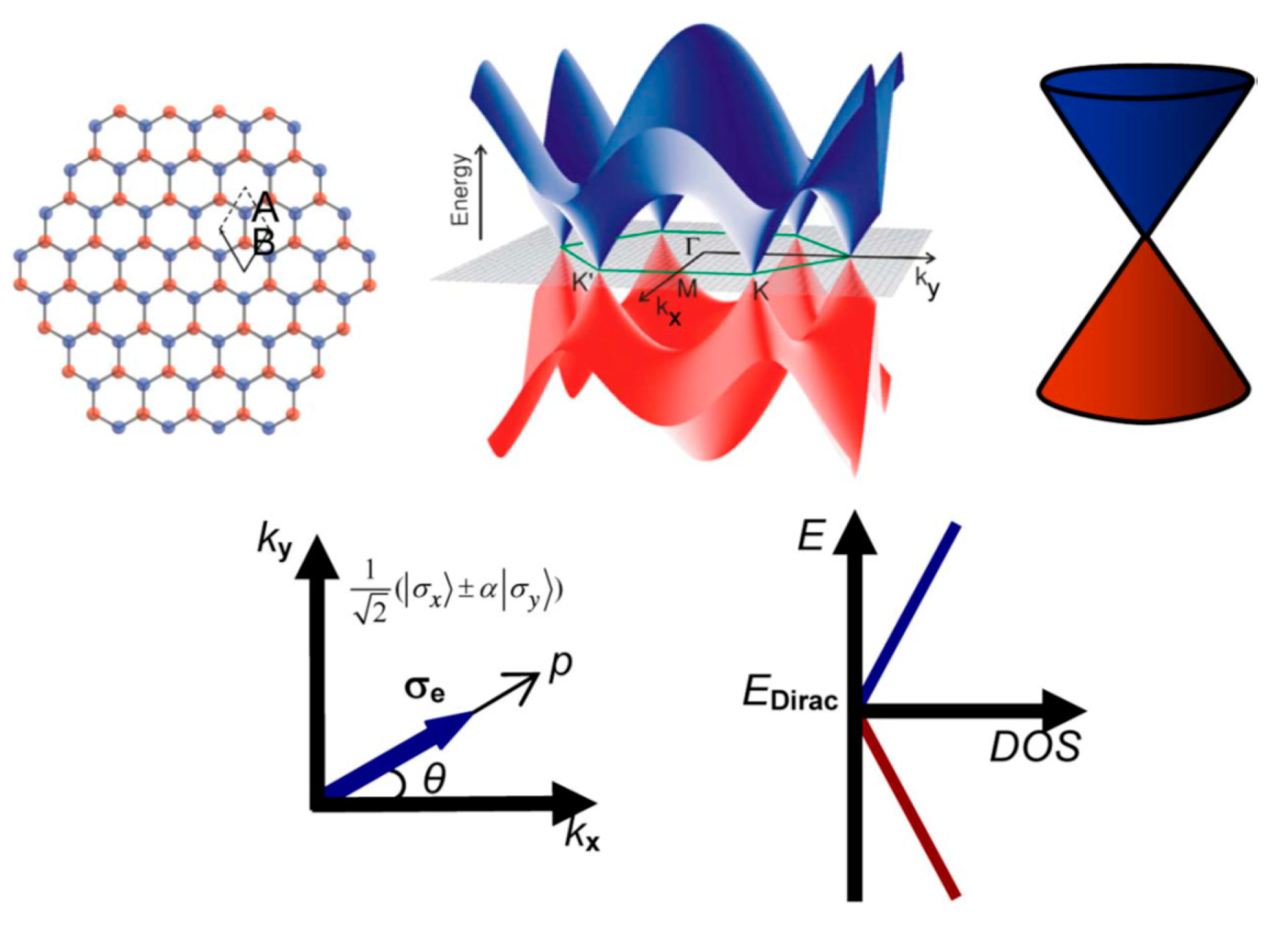
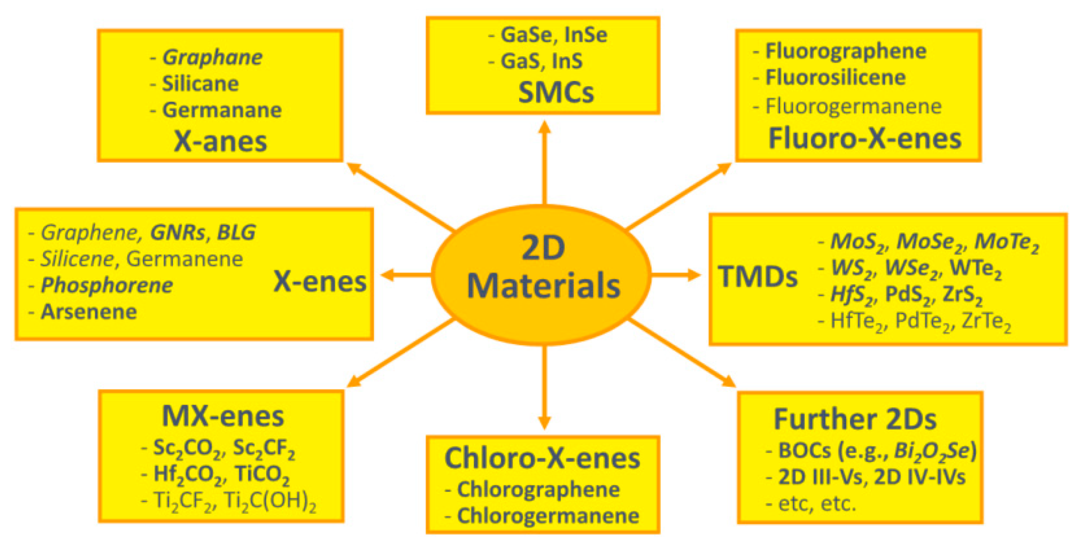
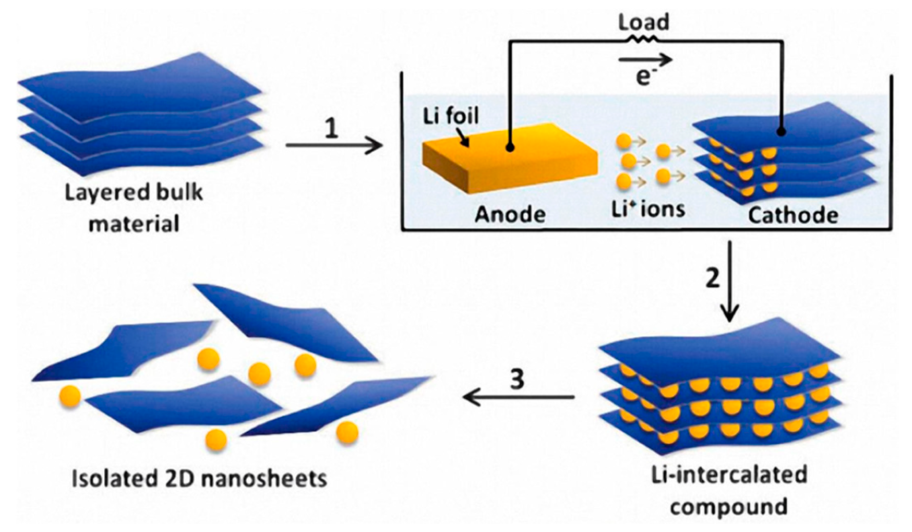
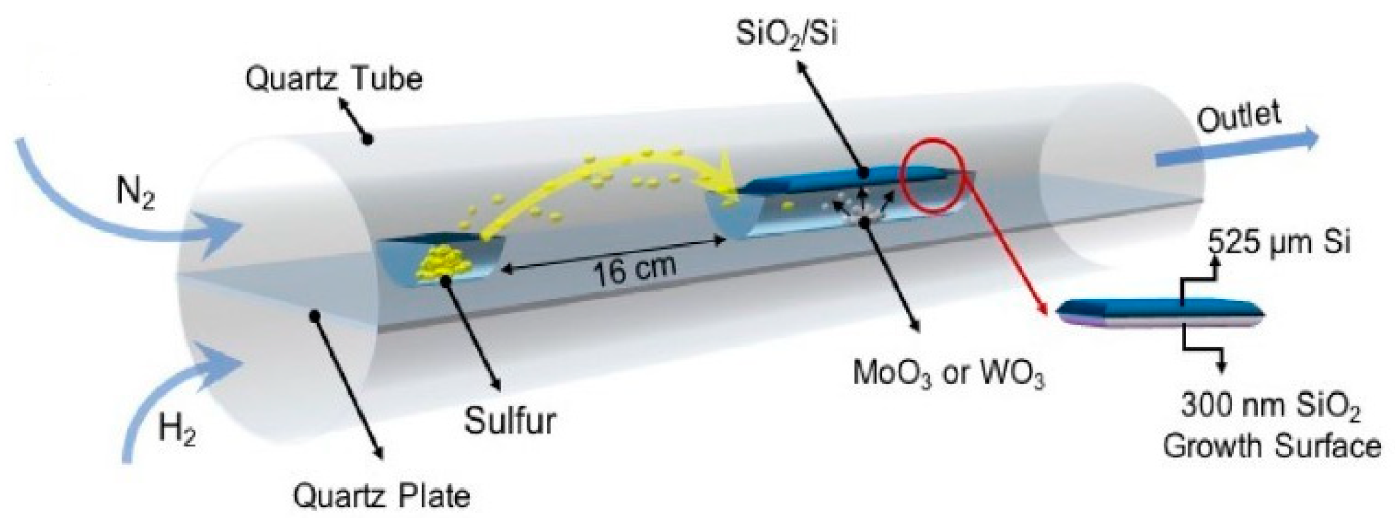
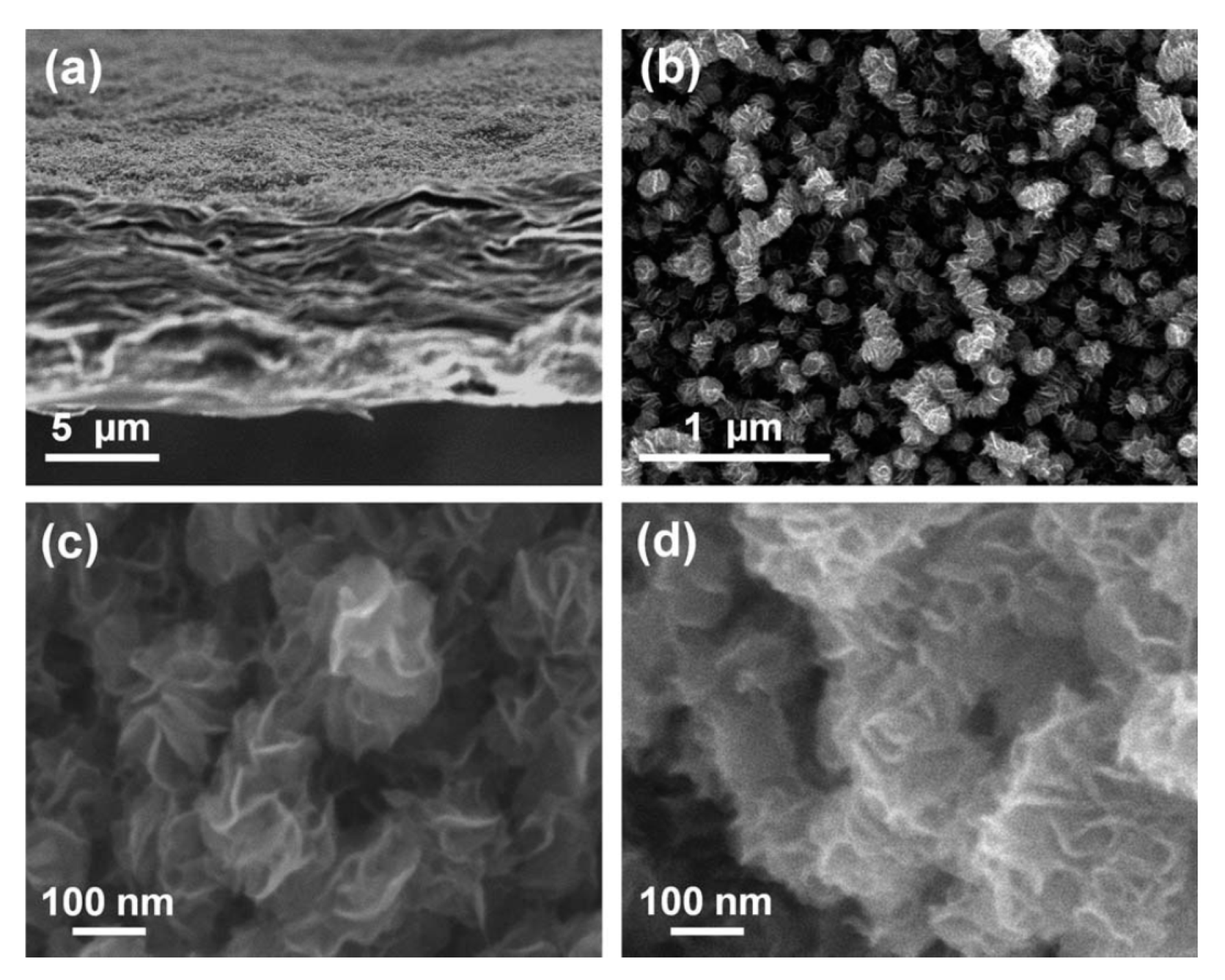
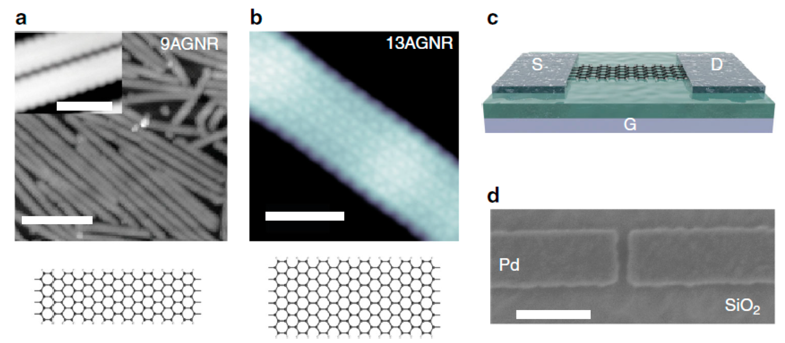
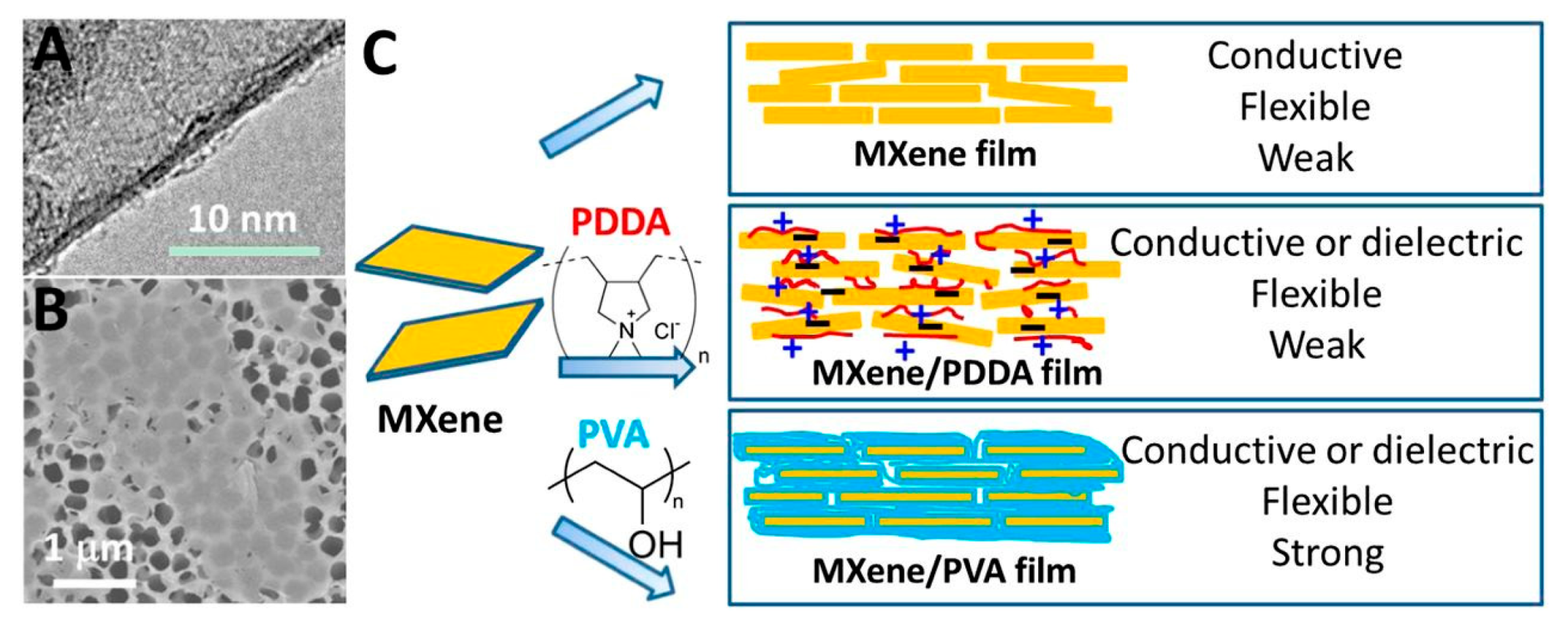
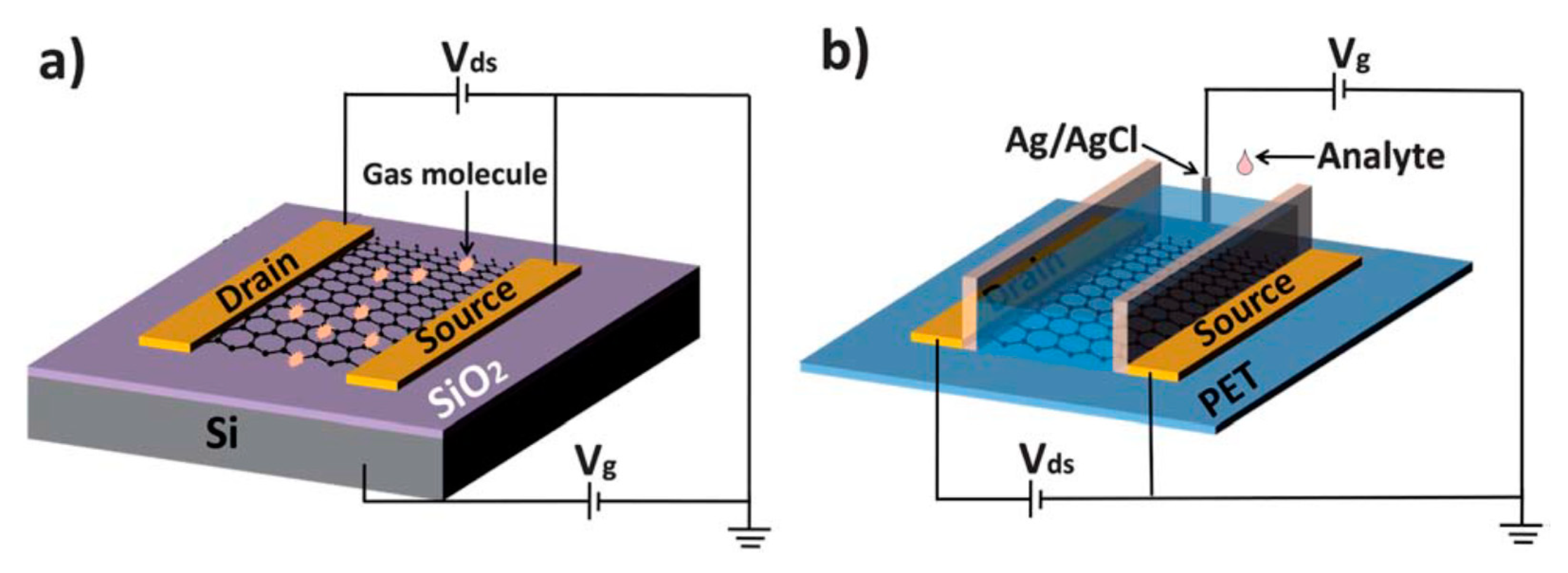
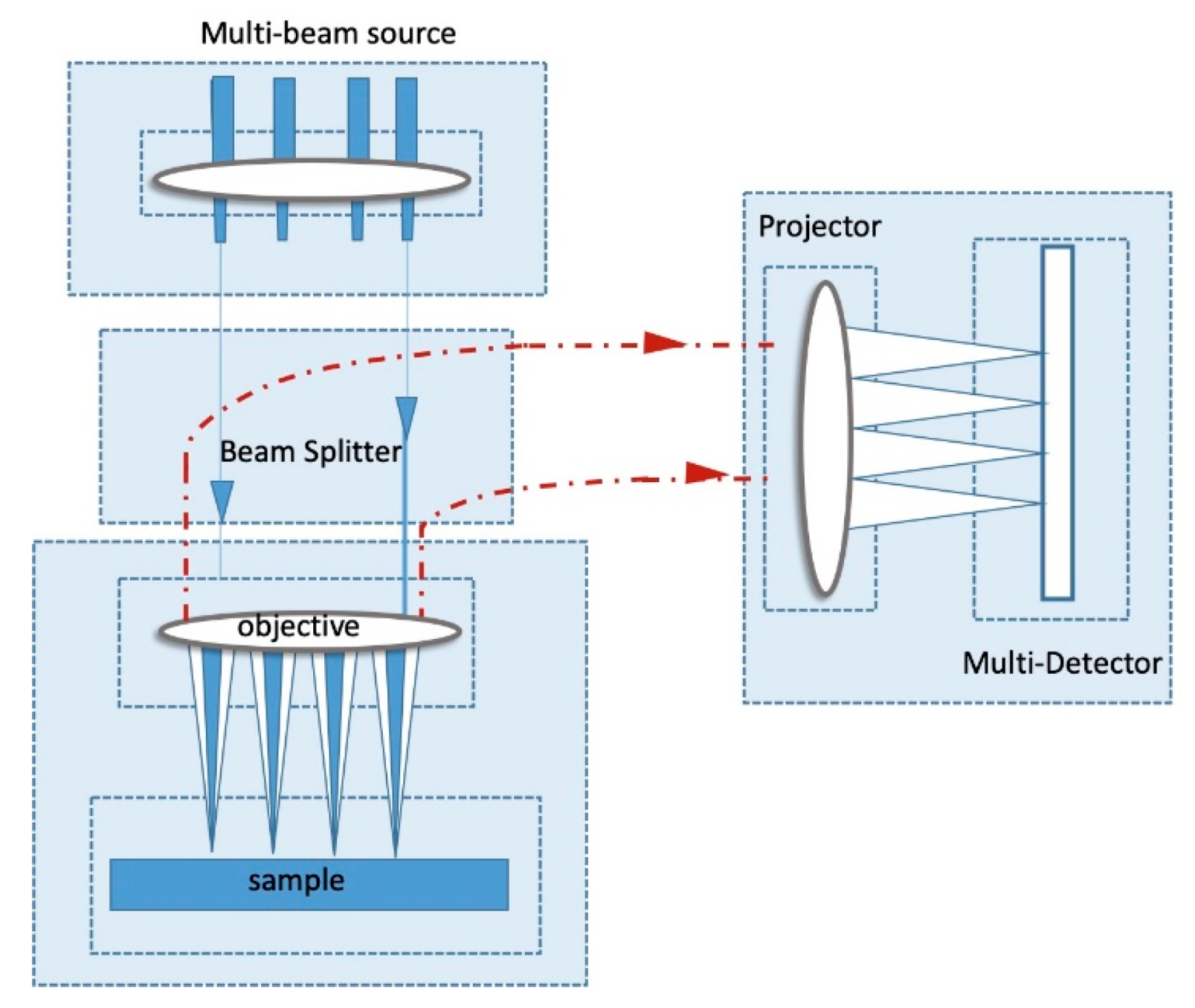
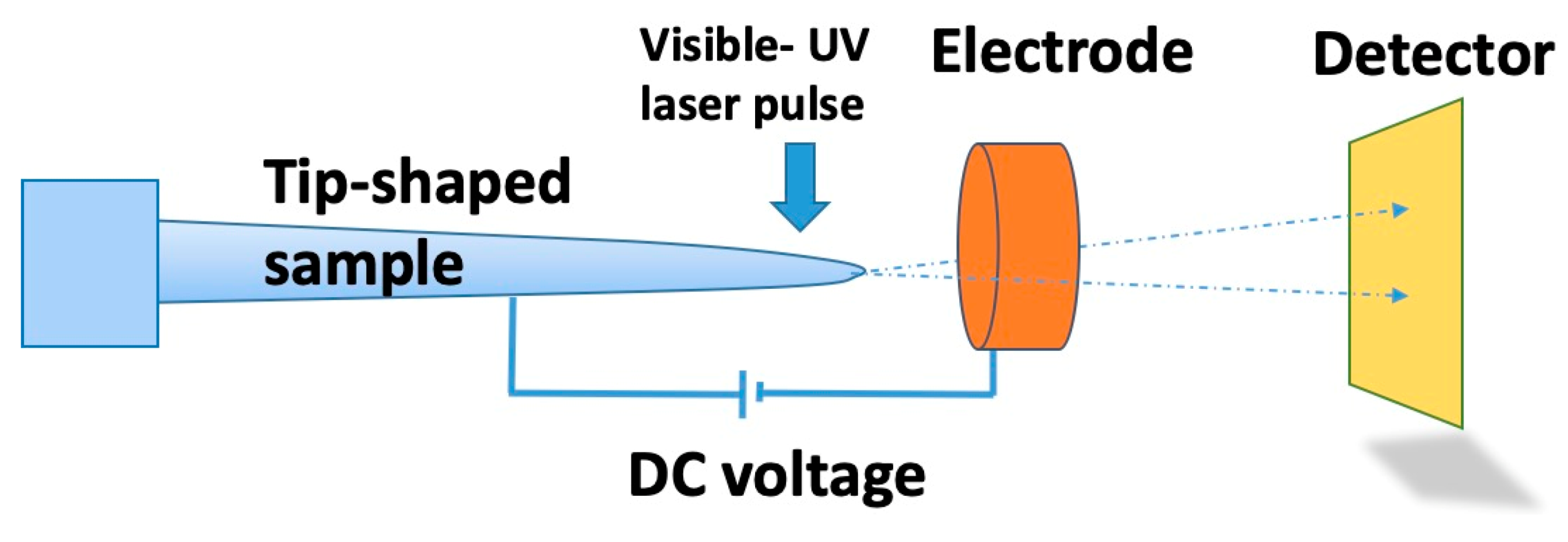
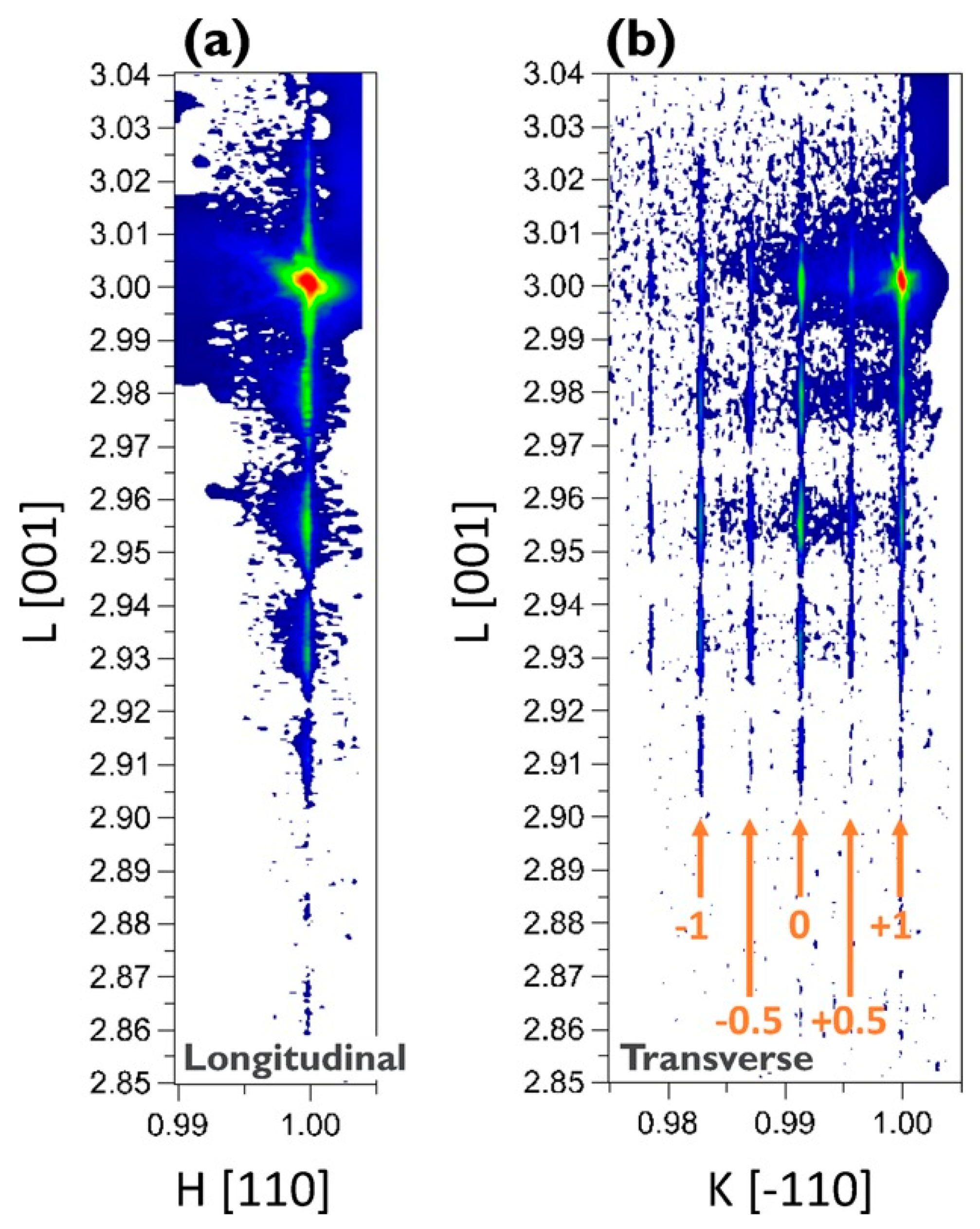
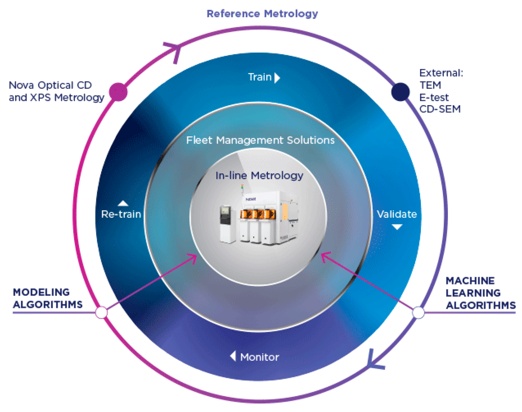
| Metal | Dep. Method | Effective Workfunction | Ref |
|---|---|---|---|
| TiN | thermal ALD | 5.3 eV | [146] |
| Ti1−xAlxN | PEALD | 5.04 eV | [147] |
| TiC-TiN | PEALD | 5.0-4.6 eV | [148] |
| TiCxNy | PEALD | 4.66 eV | [149] |
| TaCy | PEALD | 4.77−4.54 eV | [150] |
| TiC | PEALD | 5.24–4.45 eV | [151] |
| TaCN | PEALD | 4.37 eV | [152] |
| WC0.4 | PEALD | 4.2 ±0.1 eV | [153] |
| TiAlC | thermal ALD | 4.79–4.49 eV | [154] |
| TiAlC | thermal ALD | 4.4 –4.24 eV | [155] |
| TaAlC | thermal ALD | 4.74–4.49 eV | [156] |
| TaAlC | thermal ALD | 4.65–4.26 eV | [157] |
| ErC2 | ALD | 3.9 eV | [158] |
| No. | Application | Performances | Gate Length (nm) | Ref. |
|---|---|---|---|---|
| 1 | Receiver and transmitter front-ends | 850 GHz band 20 dB average receiver noise figure | 25 | [351] |
| 2 | Multiplier Chain | 400 GHz band Peak output power: 6.9 mW | 25 | [352] |
| 3 | Cascode amplifier | 17 dB gain Noise 8.3 dB 300 GHz band | 30 | [353] |
| 4 | Optical repeater | Speed 40 Gbits/s | 100 | [354] |
| 5 | Photo receiver | Speed 40 Gbits/s | 100 | [355] |
| 6 | Ultra wideband impulse Radar | 24 GHz band | 130 | [356] |
| 7 | UP-Converter | Gain of 1 dB at 64.5 GHz for 1.7 dBm LO power | 200 | [357] |
| No. | Gate Length (nm) | (mS/mm) | (mA/mm) | Ref. | ||
|---|---|---|---|---|---|---|
| 1 | 300 | 229 | 116 | 701 | ≈400 | [376] |
| 2 | 120 | 340 | 166 | 1100 | 800 | [377] |
| 3 | 100 | 415 | 249 | 1051 | 724 | [378] |
| 4 | 80 | 330 | 310 | 2630 | 700 | [379] |
| 5 | 60 | 478 | 710 | 2114 | ≈650 | [380] |
| 6 | 40 | 402 | 491 | 2000 | ≈800 | [381] |
| 7 | 30 | 681 | 644 | 1900 | ≈850 | [382] |
| 8 | 25 | 1500 | 610 | 3100 | ≈1180 | [375] |
© 2020 by the authors. Licensee MDPI, Basel, Switzerland. This article is an open access article distributed under the terms and conditions of the Creative Commons Attribution (CC BY) license (http://creativecommons.org/licenses/by/4.0/).
Share and Cite
Radamson, H.H.; Zhu, H.; Wu, Z.; He, X.; Lin, H.; Liu, J.; Xiang, J.; Kong, Z.; Xiong, W.; Li, J.; et al. State of the Art and Future Perspectives in Advanced CMOS Technology. Nanomaterials 2020, 10, 1555. https://doi.org/10.3390/nano10081555
Radamson HH, Zhu H, Wu Z, He X, Lin H, Liu J, Xiang J, Kong Z, Xiong W, Li J, et al. State of the Art and Future Perspectives in Advanced CMOS Technology. Nanomaterials. 2020; 10(8):1555. https://doi.org/10.3390/nano10081555
Chicago/Turabian StyleRadamson, Henry H., Huilong Zhu, Zhenhua Wu, Xiaobin He, Hongxiao Lin, Jinbiao Liu, Jinjuan Xiang, Zhenzhen Kong, Wenjuan Xiong, Junjie Li, and et al. 2020. "State of the Art and Future Perspectives in Advanced CMOS Technology" Nanomaterials 10, no. 8: 1555. https://doi.org/10.3390/nano10081555