
Investigation of High-Q Lithium Niobate-Based Double Ring Resonator Used in RF Signal Modulation
 and
and 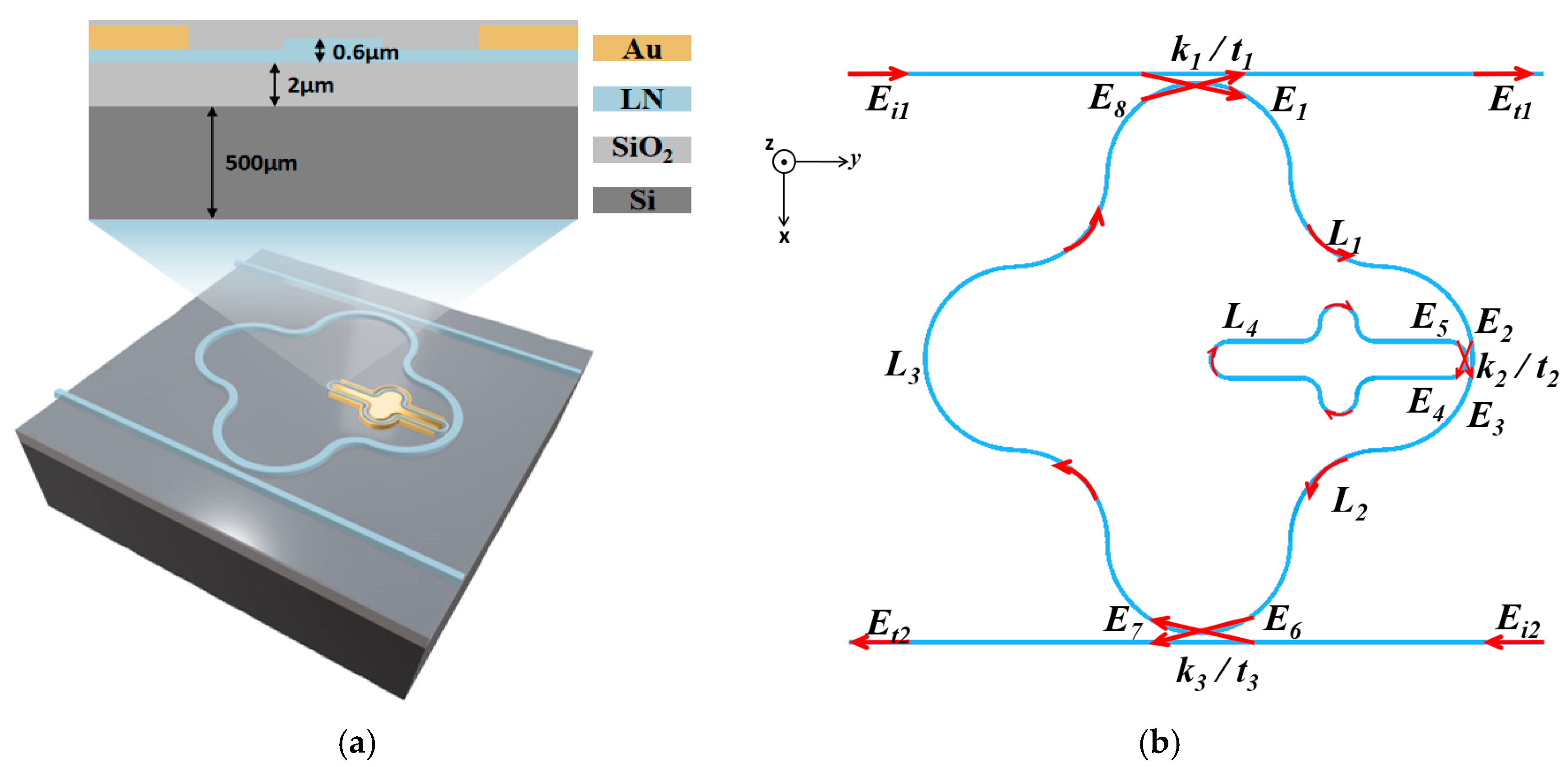
Abstract
:1. Introduction
2. Materials and Methods
3. Results and Discussion
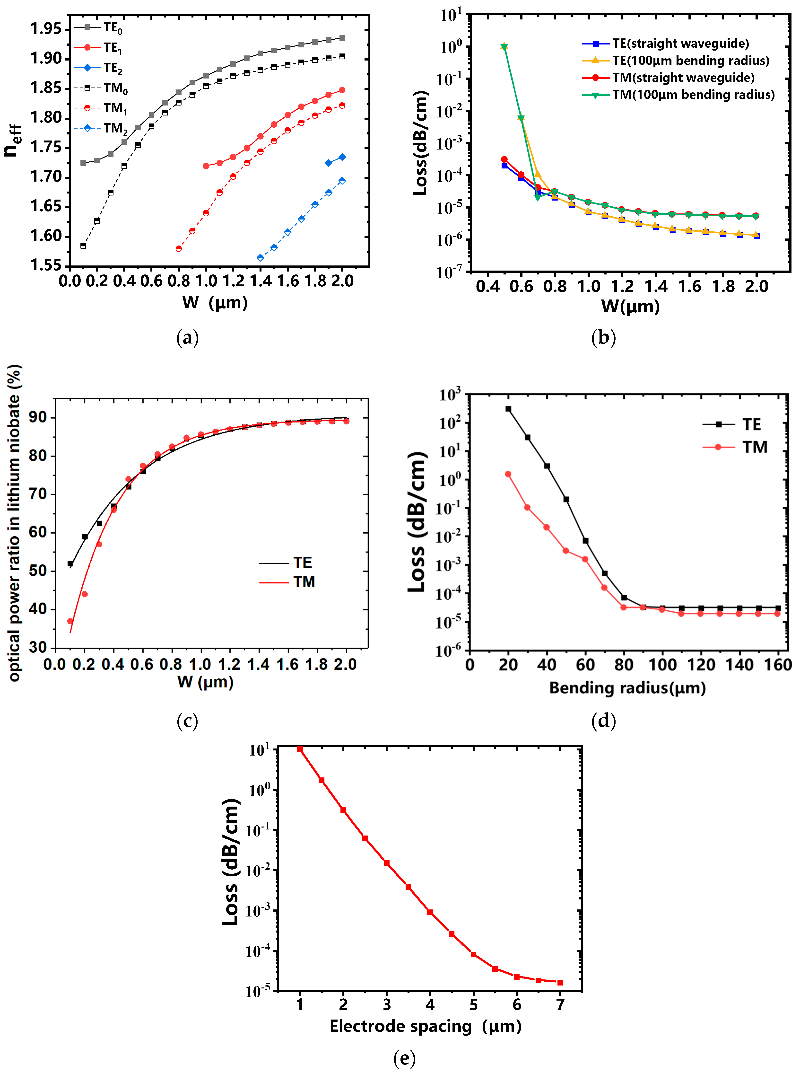
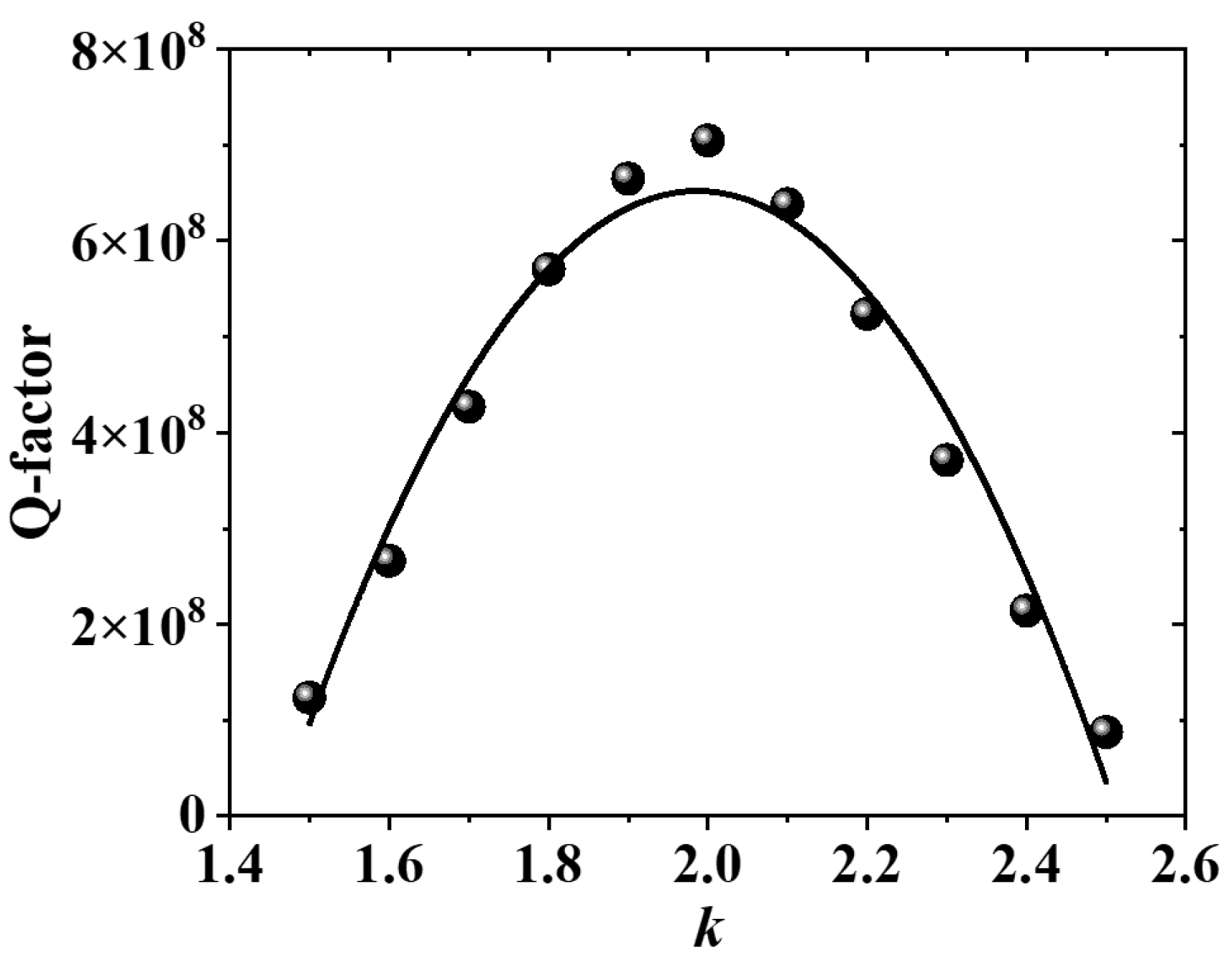
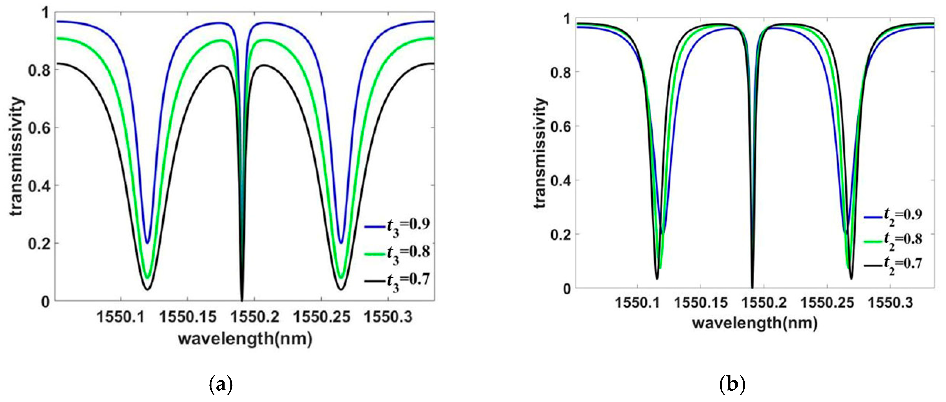
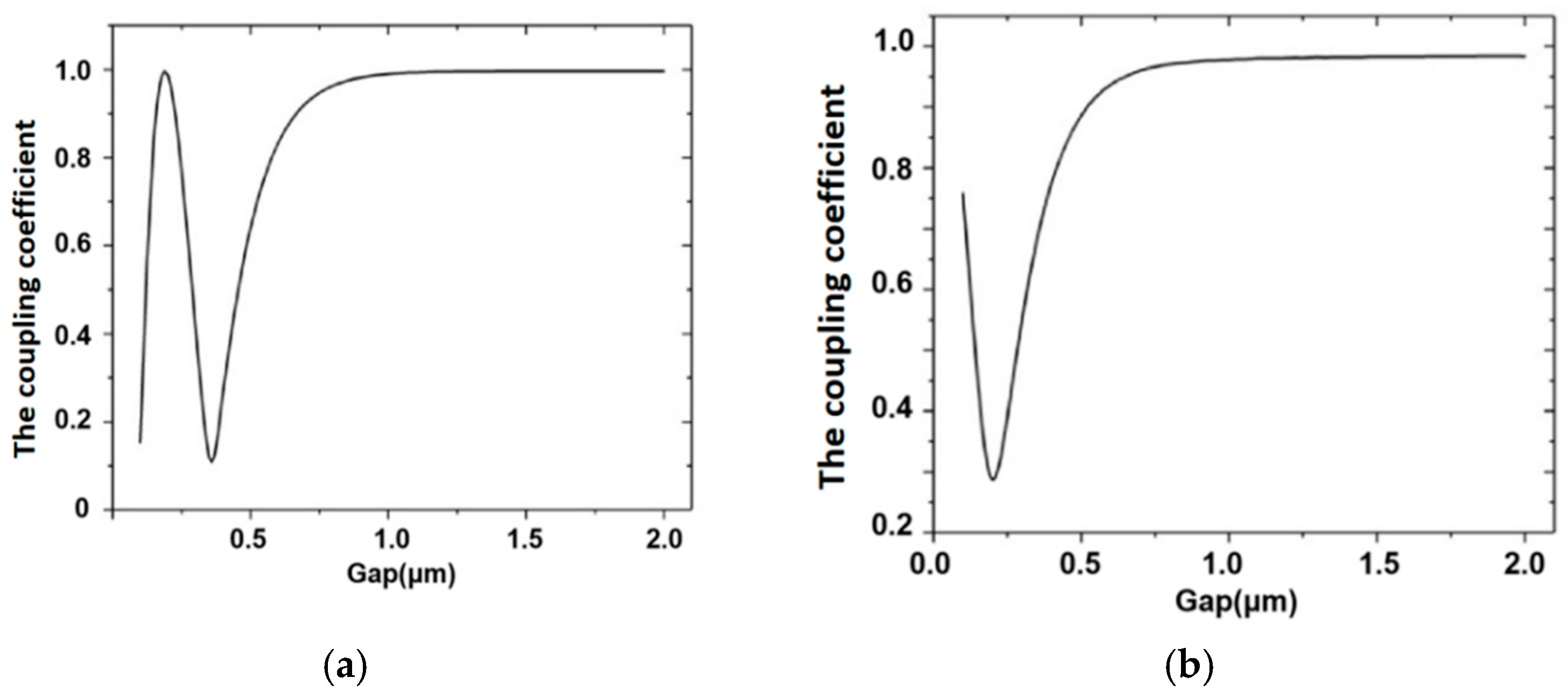
3.1. Optimization Design of the Waveguide Parameters
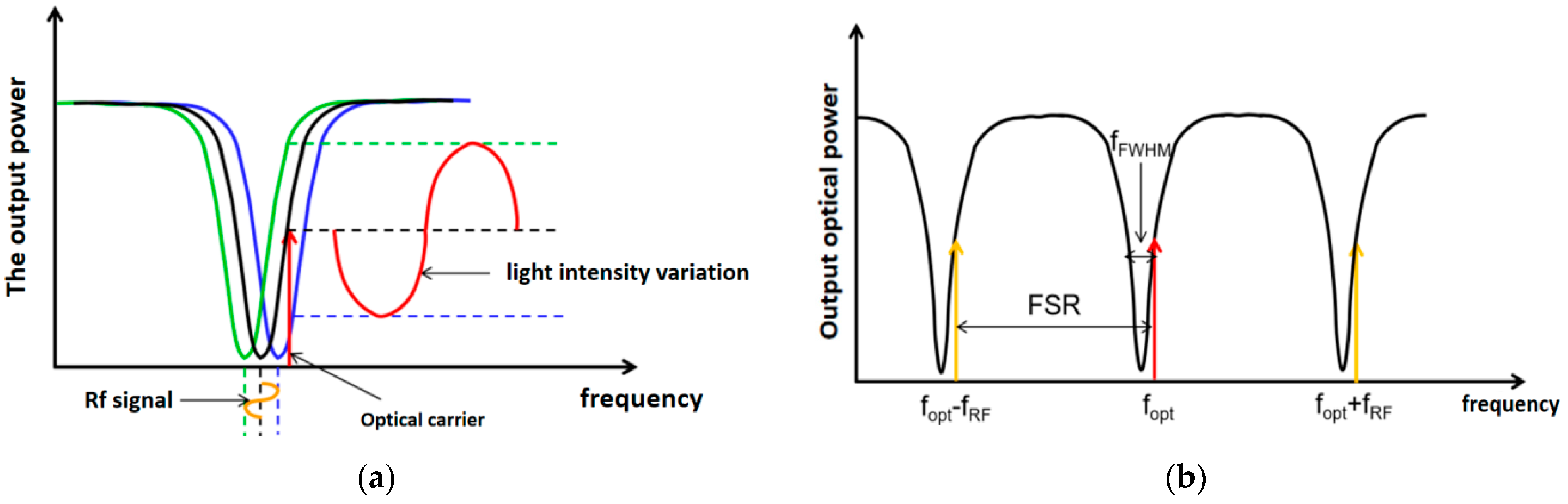
3.2. Modulation Mechanism of the Microring Resonator
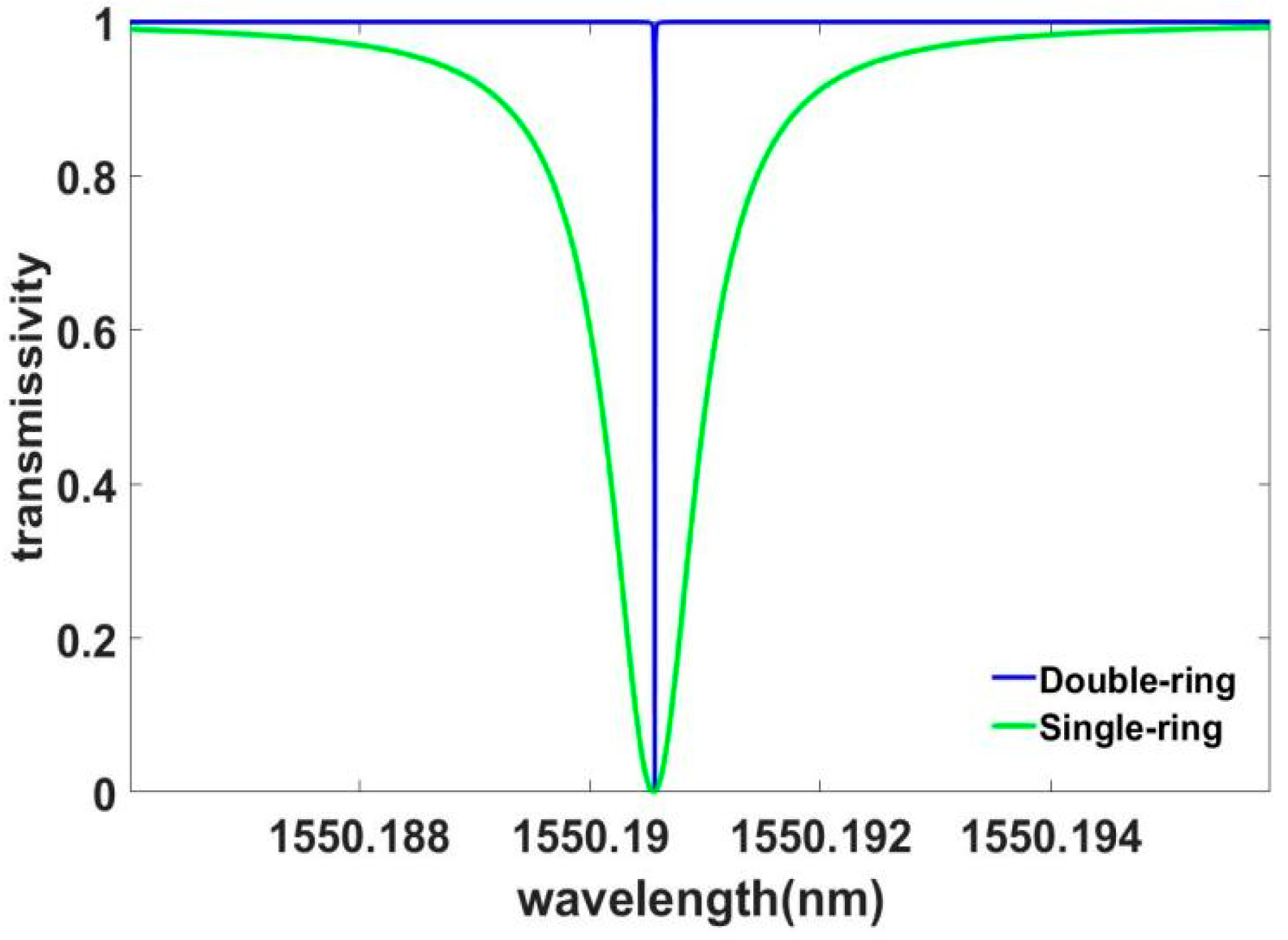
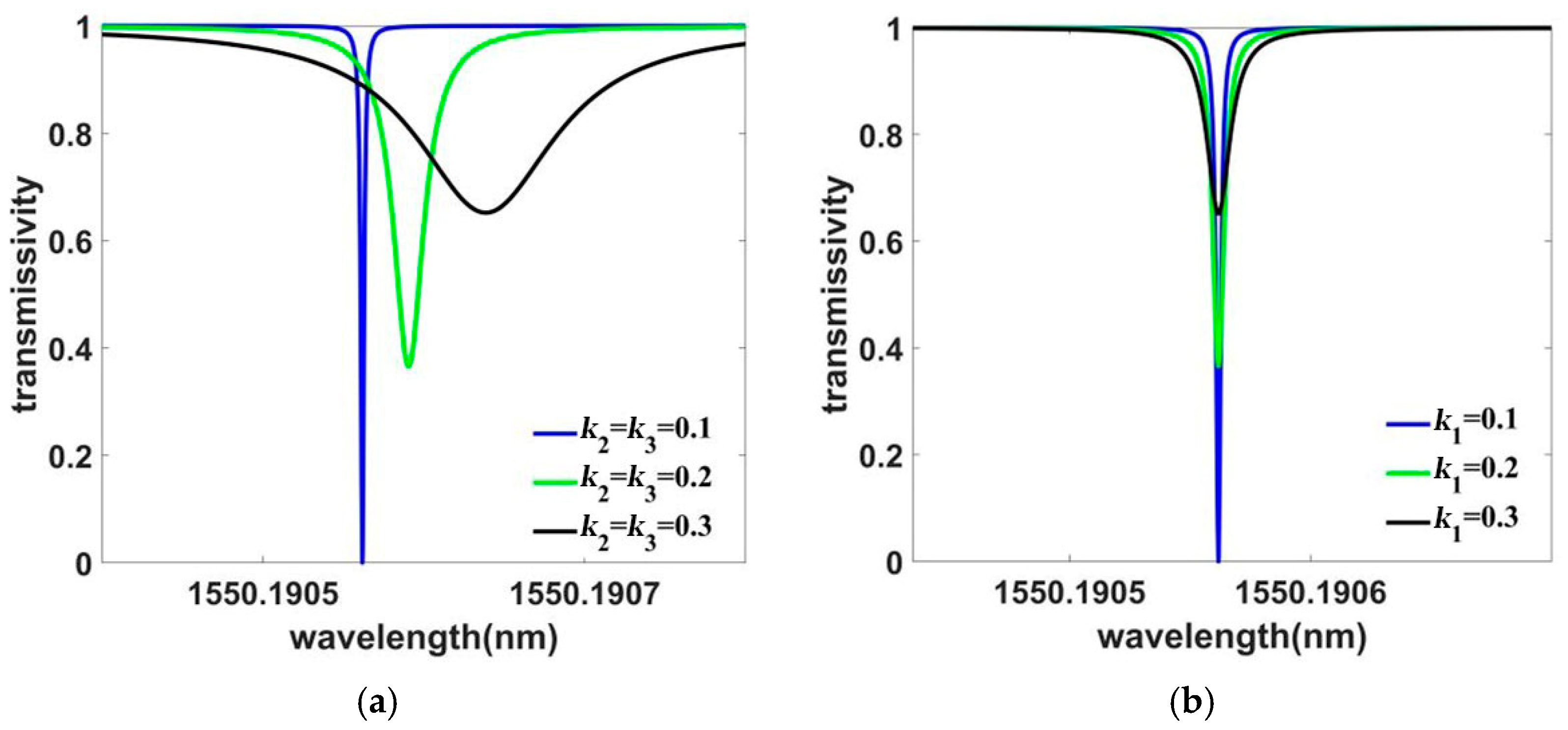
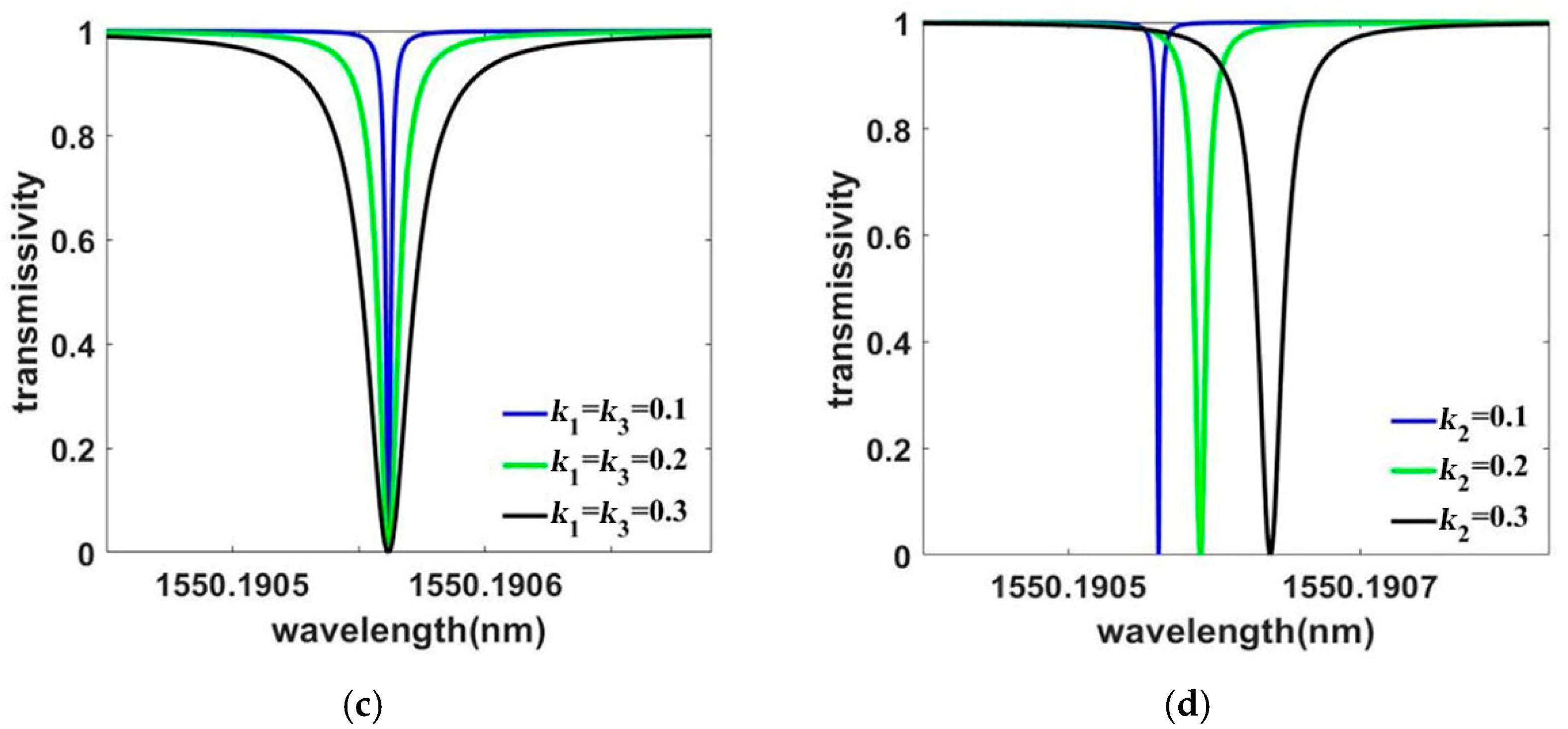
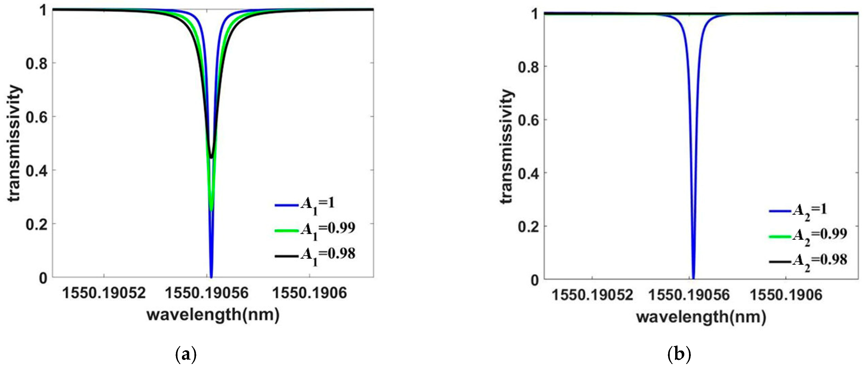
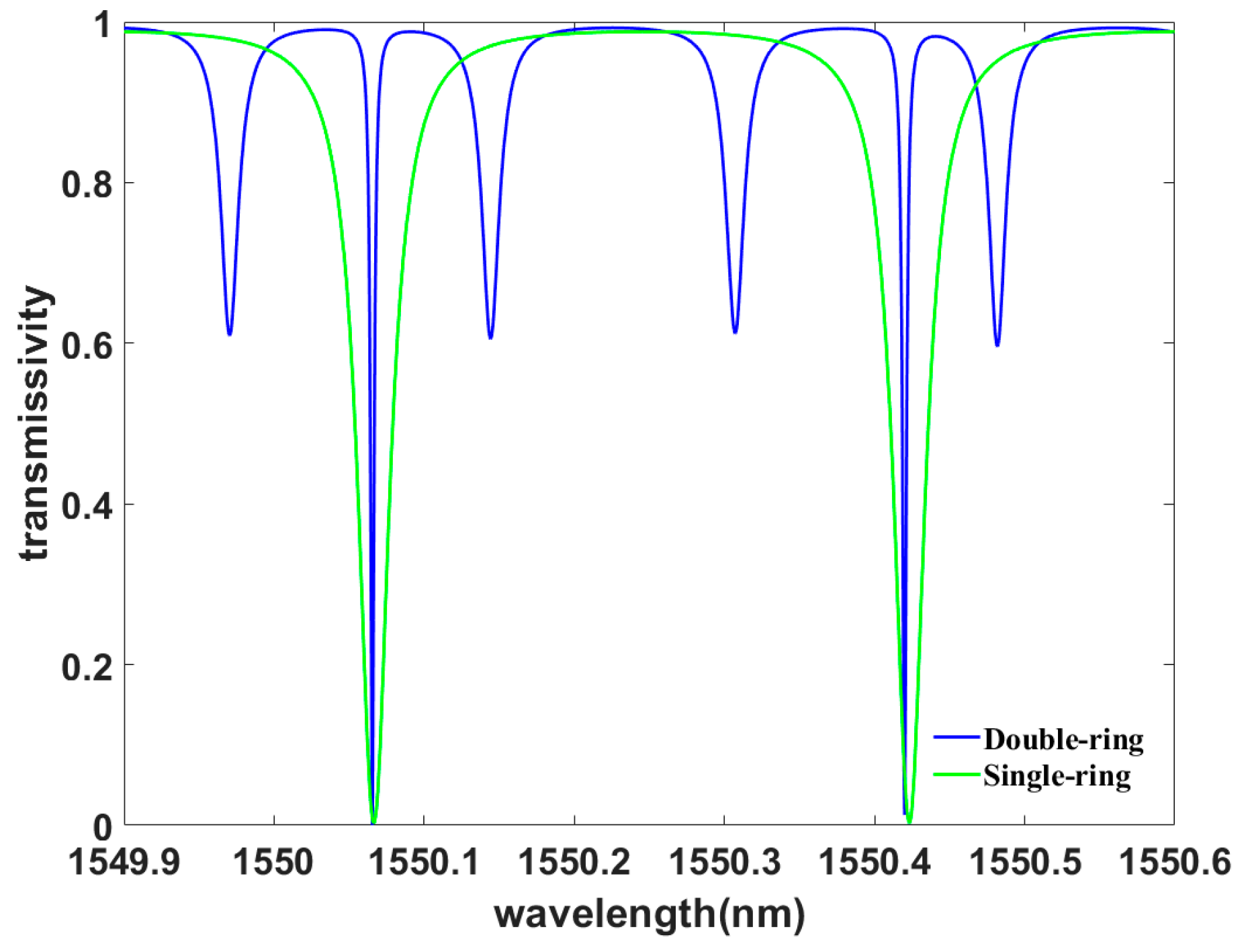
3.3. Analysis of Double Ring Structure
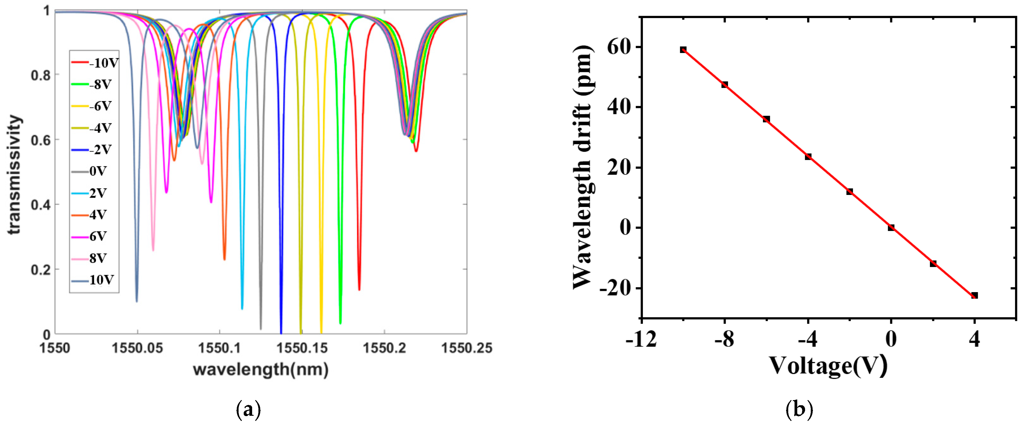
3.4. Double Ring Electro-Optic Modulator
4. Conclusions
Author Contributions
Funding
Institutional Review Board Statement
Informed Consent Statement
Data Availability Statement
Acknowledgments
Conflicts of Interest
References
- Law, F.K.; Uddin, M.R. Digital electro-optic exclusive OR and NOR gates utilizing a single micro-ring resonator. Optik 2020, 200, 163361. [Google Scholar] [CrossRef]
- Pandey, A.; Jeyaselvan, V.; Selvaraja, S.K. Broadband optical single sideband generation using an ultra high shape-factor self coupled ring resonator. Opt. Commun. 2020, 461, 125224. [Google Scholar] [CrossRef]
- Zhu, D.; Shao, L.; Yu, M.; Cheng, R.; Desiatov, B.; Xin, C.; Hu, Y.; Holzgrafe, J.; Ghosh, S.; Shams-Ansari, A. Integrated photonics on thin-film lithium niobate. Adv. Opt. Photonics 2021, 13, 242–352. [Google Scholar] [CrossRef]
- Luan, E.; Yun, H.; Laplatine, L.; Dattner, Y.; Ratner, D.M.; Cheung, K.C.; Chrostowski, L. Enhanced sensitivity of subwavelength multibox waveguide microring resonator label-free biosensors. IEEE J. Sel. Top. Quantum Electron. 2018, 25, 1–11. [Google Scholar] [CrossRef]
- Wan, L.; Chandrahalim, H.; Chen, C.; Chen, Q.; Mei, T.; Oki, Y.; Nishimura, N.; Guo, L.J.; Fan, X. On-chip, high-sensitivity temperature sensors based on dye-doped solid-state polymer microring lasers. Appl. Phys. Lett. 2017, 111, 061109. [Google Scholar] [CrossRef]
- Han, H.; Xiang, B. Integrated electro-optic modulators in x-cut lithium niobate thin film. Optik 2020, 212, 164691. [Google Scholar] [CrossRef]
- Wang, C.; Zhang, M.; Stern, B.; Lipson, M.; Lončar, M. Nanophotonic lithium niobate electro-optic modulators. Opt. Express 2018, 26, 1547–1555. [Google Scholar] [CrossRef] [Green Version]
- Buscaino, B.; Zhang, M.; Lončar, M.; Kahn, J.M. Design of efficient resonator-enhanced electro-optic frequency comb generators. J. Light. Technol. 2020, 38, 1400–1413. [Google Scholar] [CrossRef]
- Dong, P. Silicon photonic integrated circuits for wavelength-division multiplexing applications. IEEE J. Sel. Top. Quantum Electron. 2016, 22, 370–378. [Google Scholar] [CrossRef]
- Wang, S.; Feng, X.; Gao, S.; Shi, Y.; Dai, T.; Yu, H.; Tsang, H.-K.; Dai, D. On-chip reconfigurable optical add-drop multiplexer for hybrid wavelength/mode-division-multiplexing systems. Opt. Lett. 2017, 42, 2802–2805. [Google Scholar] [CrossRef]
- Li, Z.; Guo, Z.; Li, X.; Xie, R.; Xue, H.; Bai, L.; Wang, Z. Graphene light modulator based on dual-ring resonator structure. Opt. Quantum Electron. 2020, 52, 1–12. [Google Scholar] [CrossRef]
- Zhang, C.; Morton, P.A.; Khurgin, J.B.; Peters, J.D.; Bowers, J.E. Ultralinear heterogeneously integrated ring-assisted Mach–Zehnder interferometer modulator on silicon. Optica 2016, 3, 1483–1488. [Google Scholar] [CrossRef] [Green Version]
- Ahmed, A.N.R.; Shi, S.; Zablocki, M.; Yao, P.; Prather, D.W. Tunable hybrid silicon nitride and thin-film lithium niobate electro-optic microresonator. Opt. Lett. 2019, 44, 618–621. [Google Scholar] [CrossRef] [PubMed] [Green Version]
- Zhang, M.; Wang, C.; Cheng, R.; Shams-Ansari, A.; Lončar, M. Monolithic ultra-high-Q lithium niobate microring resonator. Optica 2017, 4, 1536–1537. [Google Scholar] [CrossRef]
- Qiu, F.; Han, Y. Electro-optic polymer ring resonator modulators. Chin. Opt. Lett. 2021, 19, 041301. [Google Scholar] [CrossRef]
- Boes, A.; Corcoran, B.; Chang, L.; Bowers, J.; Mitchell, A. Status and potential of lithium niobate on insulator (LNOI) for photonic integrated circuits. Laser Photonics Rev. 2018, 12, 1700256. [Google Scholar] [CrossRef]
- Bahadori, M.; Yang, Y.; Goddard, L.L.; Gong, S. High performance fully etched isotropic microring resonators in thin-film lithium niobate on insulator platform. Opt. Express 2019, 27, 22025–22039. [Google Scholar] [CrossRef] [Green Version]
- Cai, L.; Kong, R.; Wang, Y.; Hu, H. Channel waveguides and y-junctions in x-cut single-crystal lithium niobate thin film. Opt. Express 2015, 23, 29211–29221. [Google Scholar] [CrossRef]
- Wang, Y.; Chen, Z.; Cai, L.; Jiang, Y.; Zhu, H.; Hu, H. Amorphous silicon-lithium niobate thin film strip-loaded waveguides. Opt. Mater. Express 2017, 7, 4018–4028. [Google Scholar] [CrossRef]
- Jin, S.; Xu, L.; Zhang, H.; Li, Y. LiNbO3 thin-film modulators using silicon nitride surface ridge waveguides. IEEE Photonics Technol. Lett. 2015, 28, 736–739. [Google Scholar] [CrossRef]
- Wu, R.; Wang, M.; Xu, J.; Qi, J.; Chu, W.; Fang, Z.; Zhang, J.; Zhou, J.; Qiao, L.; Chai, Z. Long low-loss-litium niobate on insulator waveguides with sub-nanometer surface roughness. Nanomaterials 2018, 8, 910. [Google Scholar] [CrossRef] [PubMed] [Green Version]
- Zhang, K.; Chen, Z.; Feng, H.; Wong, W.-H.; Pun, E.Y.-B.; Wang, C. High-Q lithium niobate microring resonators using lift-off metallic masks. Chin. Opt. Lett. 2021, 19, 060010. [Google Scholar] [CrossRef]
- Zhou, Z.; Zhang, S. Electro-optically tunable racetrack dual microring resonator with a high quality factor based on a Lithium Niobate-on-insulator. Opt. Commun. 2020, 458, 124718. [Google Scholar] [CrossRef]


Disclaimer/Publisher’s Note: The statements, opinions and data contained in all publications are solely those of the individual author(s) and contributor(s) and not of MDPI and/or the editor(s). MDPI and/or the editor(s) disclaim responsibility for any injury to people or property resulting from any ideas, methods, instructions or products referred to in the content. |
© 2023 by the authors. Licensee MDPI, Basel, Switzerland. This article is an open access article distributed under the terms and conditions of the Creative Commons Attribution (CC BY) license (https://creativecommons.org/licenses/by/4.0/).
Share and Cite
Wu, Z.; Zhang, L.; Han, S.; Lian, D.; Wu, T.; Chu, W.; Li, H.; Guo, L.; Zhao, M.; Yang, X. Investigation of High-Q Lithium Niobate-Based Double Ring Resonator Used in RF Signal Modulation. Appl. Sci. 2023, 13, 4648. https://doi.org/10.3390/app13074648
Wu Z, Zhang L, Han S, Lian D, Wu T, Chu W, Li H, Guo L, Zhao M, Yang X. Investigation of High-Q Lithium Niobate-Based Double Ring Resonator Used in RF Signal Modulation. Applied Sciences. 2023; 13(7):4648. https://doi.org/10.3390/app13074648
Chicago/Turabian StyleWu, Zhenlin, Lin Zhang, Shaoshuai Han, Di Lian, Tongfei Wu, Wenjie Chu, Haoyu Li, Lei Guo, Mingshan Zhao, and Xin Yang. 2023. "Investigation of High-Q Lithium Niobate-Based Double Ring Resonator Used in RF Signal Modulation" Applied Sciences 13, no. 7: 4648. https://doi.org/10.3390/app13074648