Article

Sensorless Current Pulsation Compensation in a Hybrid Energy Storage

Department of Electrical Drives and Machines, Faculty of Electrical Engineering and Computer Science, Lublin University of Technology, 20-618 Lublin, Poland
*
Author to whom correspondence should be addressed.
Appl. Sci. 2023, 13(4), 2252; https://doi.org/10.3390/app13042252
Submission received: 19 November 2022 / Revised: 29 January 2023 / Accepted: 8 February 2023 / Published: 9 February 2023
(This article belongs to the Collection Advanced Power Electronics in Power Networks)

Abstract

:
This paper presents a dual active bridge DC/DC converter used as an AC current compensator in a hybrid energy storage application. The AC current in the DC link appears when a three-phase, four-wire inverter operates with unbalanced output currents—for example, when trying to compensate for grid voltage unbalance. This AC current has adverse effects on the operation of the electrochemical energy storage, and it should be compensated. To achieve this, a compensator is introduced into the DC link circuit of the inverter—a DC/DC converter with a capacitor bank. The DC/DC converter is responsible for compensating the AC pulsation by creating its own pulsation with the opposite phase. In the paper, the genesis of this pulsation is explained, and a compensation circuit is proposed along with a sensorless compensation algorithm. The algorithm is based on symmetrical decomposition and is used to generate a reference signal for the compensator. The numerical analysis of the algorithm is presented, and the operation of the compensator is verified on the laboratory bench.

1. Introduction

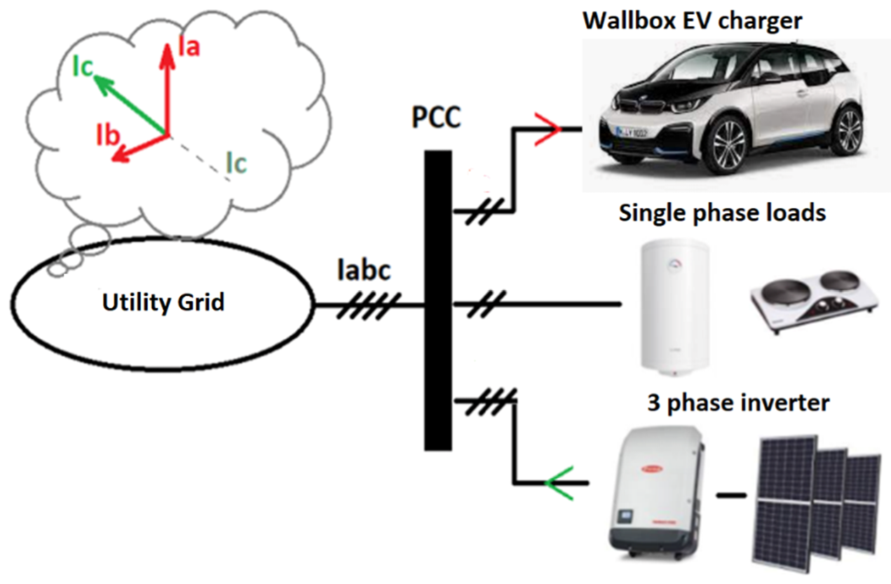
The current trends in renewable energy sources have created a significant change in the operation of the utility grid. Increasing numbers of households with photovoltaic inverters installed are viewed as local energy sources, operating in grid-feed mode. Unfortunately, it is common practice to install a three-phase inverter in the household, and the loads (TVs, household appliances, and air conditioning) are rarely connected in an optimal way—shared evenly across all three phases (Figure 1). This creates a situation where a household with a symmetrical renewable source and an asymmetrical load is seen by the distribution grid as having an asymmetrical load or asymmetrical source [1].
This situation will be much more prominent in rural areas, where the distance to a power source is significant and the household is connected to the so-called, weak grid [2]. In turn, the voltage in the area will become asymmetrical and fluctuate during the day, with negative consequences for both the household and the grid infrastructure. This situation has a negative influence on both the household devices and the grid infrastructure—for example, inverter synchronization issues or reactive power flow. In order to reduce asymmetry, a three-phase, four-wire converter (3p-4w converter) is required, along with energy storage [3,4]. Such a converter, utilizing independent power control in each of the phases, can transfer the excess energy from the underloaded phase into the overloaded one, thus achieving a reduction in the voltage asymmetry [5]. It is also possible to achieve this effect without energy storage, but such a solution would have its compensation ability limited by the DC link capacity.
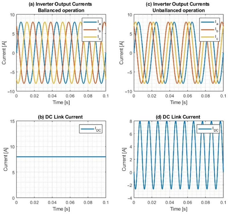
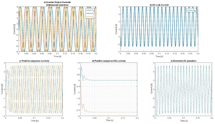
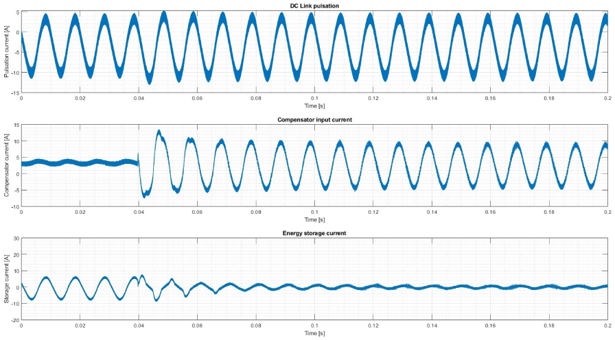
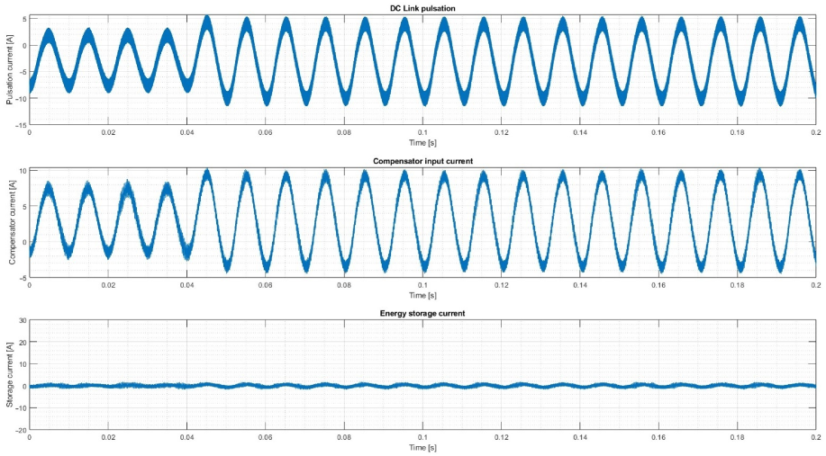
Asymmetric operation of an inverter causes a current flow in the neutral wire and creates current pulsation in the DC link [6]. This pulsation is added to the DC component of the DC link current and has a frequency two times higher than the frequency of the grid (Figure 2). This creates several issues, including increased THDi on the output of the inverter or the generation of losses in the energy storage. Losses in energy storage are turned into heat, and this effect is commonly used, in a controlled manner, to preheat the batteries before rapid charging of an electric vehicle in cold environments [7]. In a grid-tied inverter application, this effect is undesirable: since the pulsation is tied to asymmetrical output currents, it is not directly controlled and can lead to overheating of the storage. Since the energy storage usually limits its current outputs as a function of temperature, the range of operation of the storage is limited as well. Another problem is that this pulsation is often not visible to the energy storage due to the current measurement sampling time and can disrupt the state of charge (SOC) estimation, creating a faulty state in the energy storage.
Operation of the inverter during an asymmetric grid state is usually considered a problem of maintaining symmetric operation during an asymmetric grid state [8]. Another trend is the asymmetric operation of the inverter and the reduction of the voltage asymmetry in the grid. The first approach typically utilizes an inverter driven by Dual-Vector-Current-Control algorithms (DVCC), which are based on symmetrical decomposition and synchronization to the positive sequence to deliver symmetric power to the grid [9]. The approach focused on asymmetrical operation uses independent control loops for each of the phases of the inverter to inject asymmetrical currents into the grid to reduce voltage asymmetry, but it also uses symmetrical decomposition to synchronize with the grid. Commonly, additional switches are introduced to the topology of the inverter to reduce the voltage pulsation in the DC link [10].
In this paper, the approach to compensating the DC link current pulsation during asymmetrical operation of the 3f4p inverter is presented. The presented system is based on a dual-active bridge operating as a pulsation compensator. The proposed solution aims to reduce the pulsation current on the energy storage input by creating the same pulsation current, shifted by π. A similar system was presented by the authors in [11]. In this paper, the work is expanded by implementing a sensorless loop driving the compensator. The sensorless loop aims to extract the AC component of the DC link’s current pulsation without a current sensor in the DC link. Instead, the AC component is calculated based on the symmetrical decomposition of the inverter output currents.
The following section describes the genesis of the DC link pulsation and the mathematical method of its extraction, which later serves as a basis for sensorless operation of the compensator. The pulsation calculation is then numerically verified in MATLAB. Next, the proposed compensation circuit is presented along with the control loop, and the sensorless approach is then discussed. In the next section, the compensation algorithm is implemented on the laboratory bench. The operation of the compensator is then tested. The final section discusses the results achieved and potential applications.

2. DC Link Pulsation in an Energy Storage Application

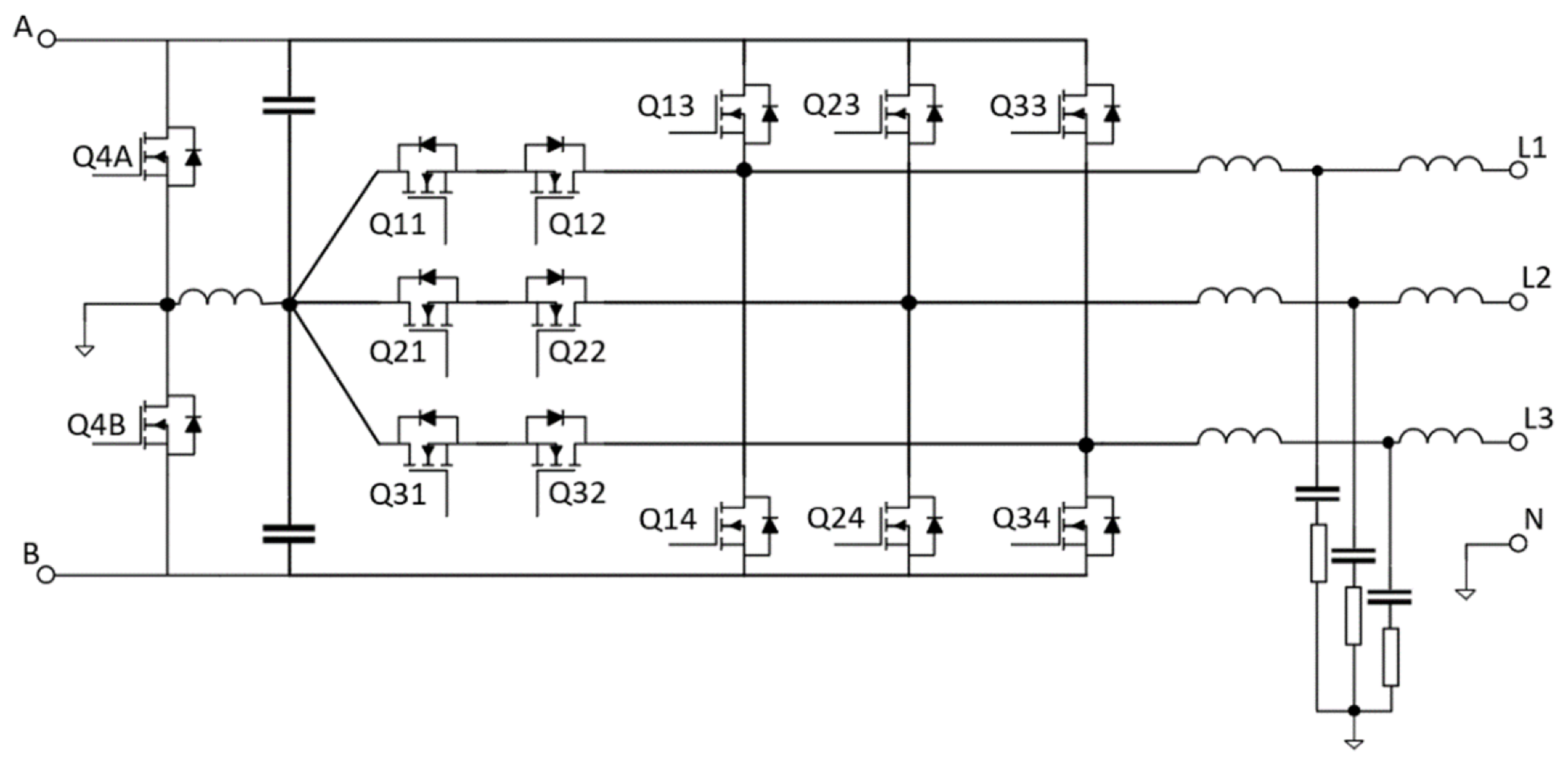
In order to symmetrize the grid, the inverter requires a four-wire structure (3p-4w). The fourth wire works as a neutral wire and can be connected to either a split capacitance of the DC Link or an additional active leg of the inverter (Figure 3). Additionally, independent phase current control needs to be implemented. A common practice for the manufacturers is to use three separate single-phase inverters in a Y-connection to serve as a 3p-4w inverter.
The analysis of such an inverter is similar: from a control standpoint, it is viewed as a trio of single-phase, Y-connected inverters, each driven by a separate control loop, for example by a proportional-resonant controller [12]. However, in order to estimate the pulsation level, the system needs to be treated as a three-phase inverter. In that case, the instantaneous output power of the inverter can be described as the sum of its powers in each of the phases, Equation (1):
p 3 f = k = 1 3 1 2 V k I k cos φ v k φ i k cos 2 ω t + φ v k + φ i k
where Vk—magnitude of the phase voltage, Ik—magnitude of the phase current, φ v k —voltage phase, φ i k —current phase, and ω = 2 π f , with f being the grid frequency.
If inverter efficiency is omitted, then this equation can be used to approximate the power drawn from the DC link. This equation can be split into time-invariant, and time-variant components. During symmetric operation of the inverter, the three time-variant components add up to zero, while during asymmetric operation they do not, which causes the cos 2 ω t + φ v k + φ i k component of the equation to reappear and transfer into the DC link as an AC current pulsation. In order to extract the AC pulsation from the DC link current, the symmetrical decomposition, Clarke and Park transforms are used (Equations (2)–(7)):
i a b c = i a i b i c = I + cos ω t cos ω t 2 π 3 cos ω t + 2 π 3 + + I cos ω t cos ω t 2 π 3 cos ω t + 2 π 3 + I 0 cos ω t cos ω t cos ω t
i α β = i α i β = I + cos ω t + + sin ω t + + + I cos ω t + sin ω t +
where I+, I, and I0 are the magnitudes of the currents of symmetrical components; ∅+ and ∅ are the phases of symmetrical components.
Positive and negative sequences can be derived using two Park transforms with reference frames rotating in opposite directions:
i d q + = i d + i q + = I + cos + sin + + I cos 2 ω t sin 2 ω t sin 2 ω t cos 2 ω t cos sin   ,
i d q = i d i q = I cos + sin + + I + cos 2 ω t ( sin 2 ω t ) sin 2 ω t cos 2 ω t cos + sin + .
These two components can be split into time invariant and time variant components:
i d q + = i d + ¯ i q + ¯ + i d + ˜ i q + ˜ = I + cos + sin + ¯ + I cos cos 2 ω t sin 2 ω t + I sin sin 2 ω t cos 2 ω t ˜
i d q = i d ¯ i q ¯ + i d ˜ i q ˜ = I + cos sin ¯ + I cos + cos 2 ω t sin 2 ω t + I sin + sin 2 ω t cos 2 ω t ˜
the positive sequence, Equation (6) is directly related to DC link pulsation, which is linked by voltage gain of the converter k:
i d c = k i d + ¯ + k i d + ˜ = k I + cos + k I cos cos 2 ω t + k I sin sin 2 ω t
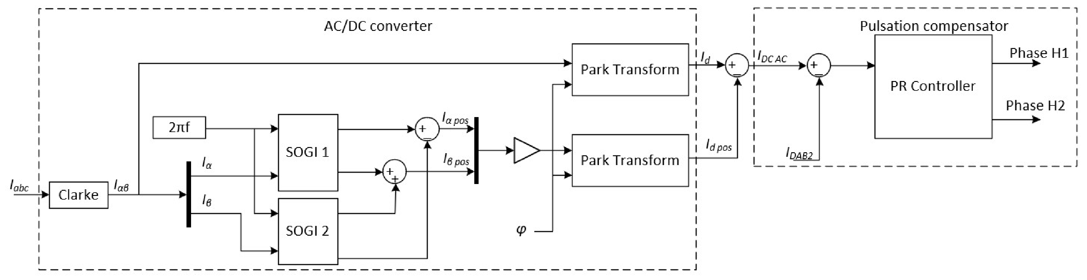
this calculated current is used to extract the pulsation value and is further passed as a current reference signal for the compensator, creating a sensorless compensation loop.
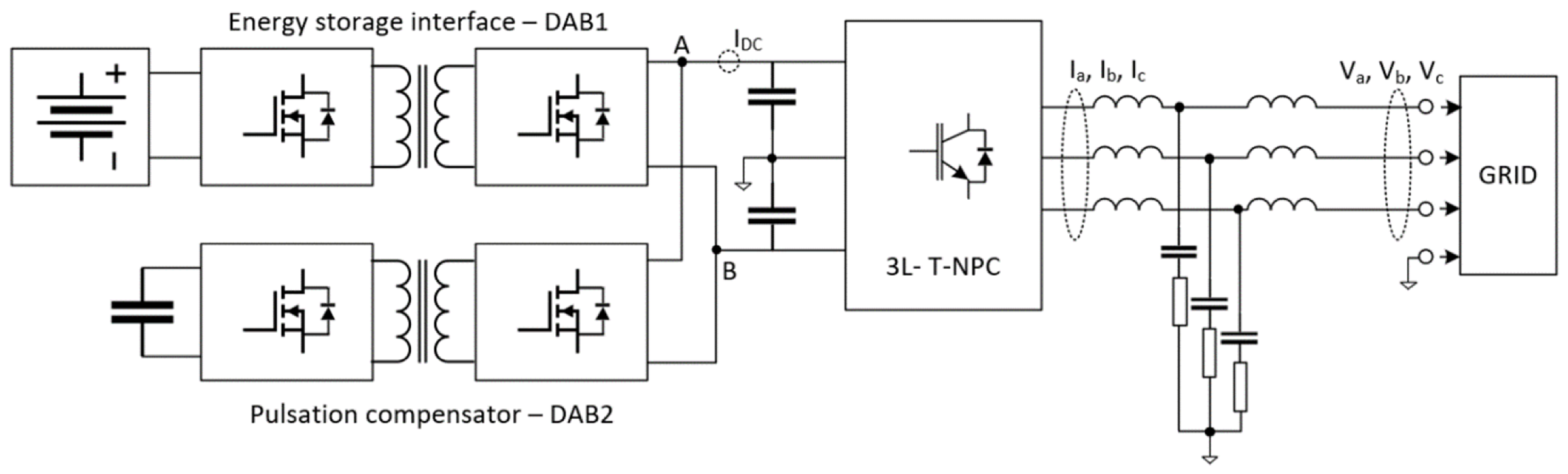
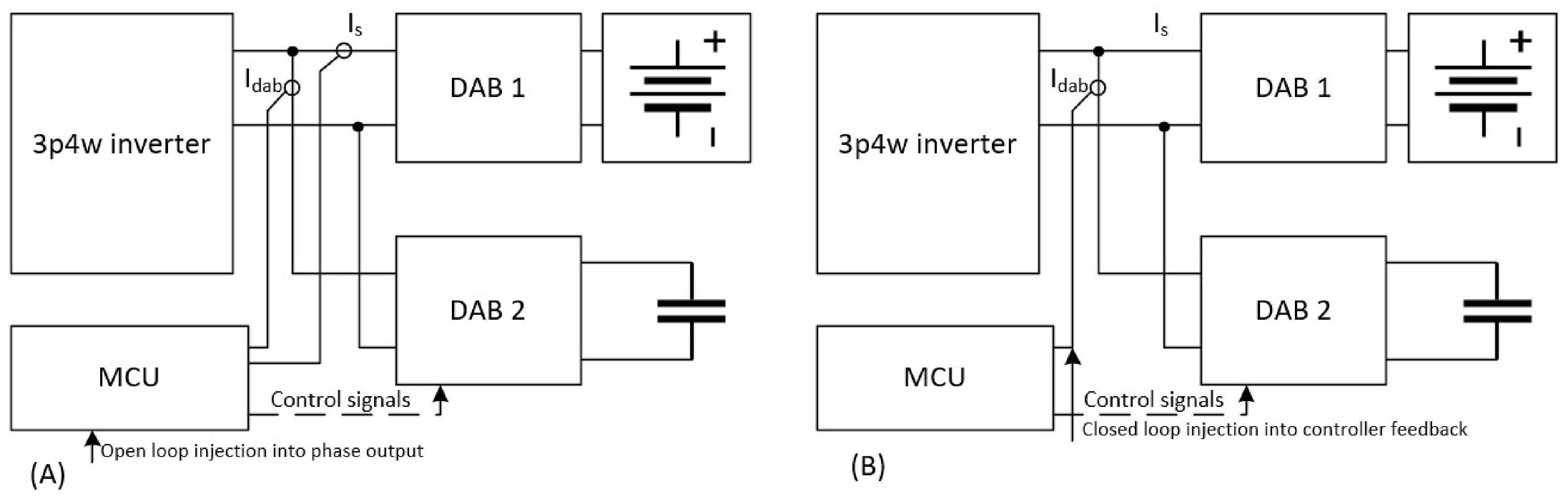
The compensation circuit, which can take over the AC component of the DC link current, is presented in Figure 4. A three-level T-NPC inverter is connected to the grid via an LCL filter. The DC link of the inverter is connected through an isolated DC/DC dual-active bridge converter (DAB1) to a lithium-ion energy storage and to the compensator—another dual-active bridge converter (DAB2), connected to the capacitor bank. The goal is to generate a sinewave with a phase opposite of the DC link pulsation current using the DC/DC converter DAB2. The dual active bridge converter was chosen for this application due to its high dynamics and large voltage gain [13]. The sensorless loop in this application is achieved by replacing the main current measurement (IDC) with calculations based on the symmetrical decomposition of the inverter output currents. Both DAB converters are still operating in sensored mode, with their respective internal current loops based on current sensors, and further reduction of the number of the sensors is possible by implementing a sensorless loop on the internal DC/DC converter level [14,15].
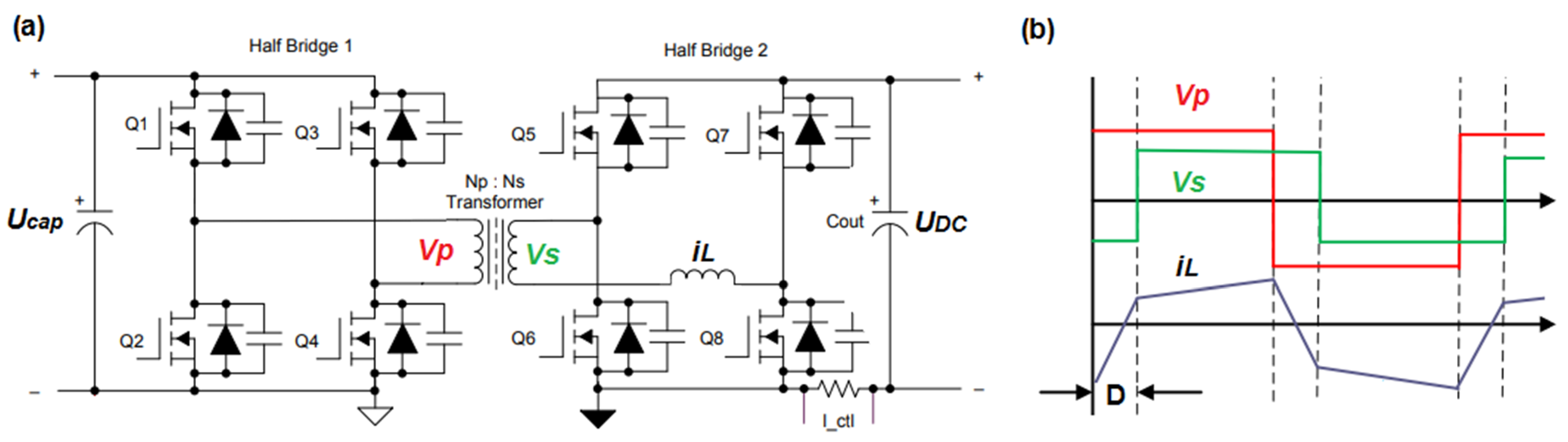
For analysis, the dual active bridge topology can be simplified into two high-frequency voltage sources connected with the leakage inductance Llk, which generate square voltage waves (Vp and Vs). The power flow is controlled by shifting the phase φ between those generated voltages (Figure 5). It is also common to describe phase shift as D, where D = φ/π. When the voltage Vp leads the voltage Vs, the power is transferred from the input to the output of the converter; when the voltage Vp lags the voltage Vs, the power is transferred from the output to the input. There is no need for separate algorithms when changing the direction of the power flow, which is desired for this application.
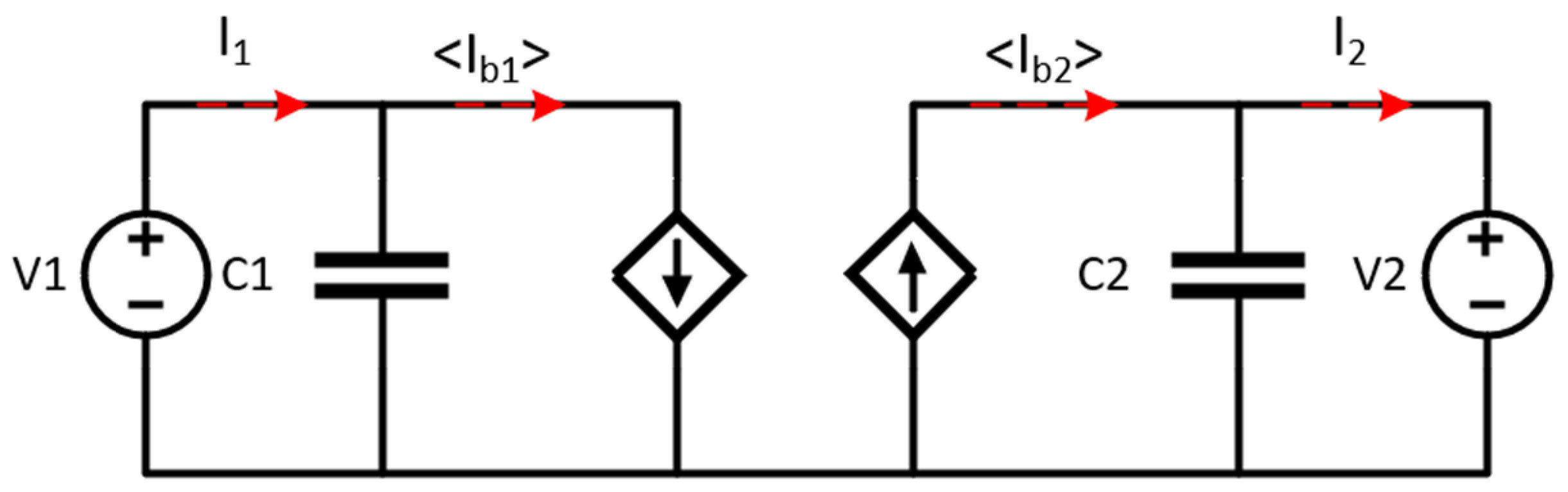
The dynamics of a dual active bridge topology depend mostly on two contributors: input and output filters, and the leakage inductance Llk of the medium frequency transformer. This makes modeling the converter problematic, as the leakage inductance operates with dynamics several orders of magnitude higher than the output filters. In [16], several modeling methods are compared against one another, with negligible differences between results mostly noticeable towards the high-frequency range. Based on those findings, for this application, the reduced order model was selected to describe the dynamics of the DAB converter. This approach ignores the dynamics of leakage inductance and uses the average values of the switching currents. Most of the papers treat the dual active bridge converter as a voltage converter, and derive the transfer function as an output voltage to control phase function. Since the compensator requires that it control the input current of the converter, the input current required to control the phase transfer function must be derived.
For the DAB converter modulation scheme, the single phase shift (SPS) control was used [17]. This scheme can be switched to extended phase shift or, to better handle rapid changes in current, to symmetrical single phase shift [18]. In the case of the SPS, the output power can be described as follows:
P o u t = n V i n V o u t φ 1 2 φ f s L l k
where n—transformer turn ratio, fs—switching frequency, and Vin, Vout—input and output voltages. The equivalent circuit for the reduced-order model is presented in Figure 6. At this stage, the switching cycle average currents are introduced: i b 1 , 𣊚 i b 2 .
Assuming ideal efficiency and symmetry, Pout = Pin, and since Pin = Vin i b 1 , ib1 can be calculated as follows:
i b 1 = n V o u t φ 1 2 φ f s L l k
a small perturbation can be injected into the <ib1>:
i b 1 = I b 1 + i b 1 ^
where I b 1 is the quiescent component and i b 1 ^ is the perturbation. This perturbation would be a response to the phase perturbation:
φ = Φ + φ ^
where Φ is the phase quiescent component and φ ^ is the phase perturbation. The transfer function from phase to input current can be obtained as follows:
G i φ s = i b 1 ^ φ ^ = n V i n 1 4 φ f s L l k
from this standpoint, the transfer function does not introduce any delays. A similar statement is presented in [19], where the transfer function (phase to output voltage) is described as:
G d a b s = V d T s 2 L l k 1 2 D Z o s
where D—phase shift, Vd—input voltage, Ts—switching period, and Zo(s)—transfer function of the output filter. Division by Zo(s) creates a transfer function from the phase to the output current. The cited paper states that in order for this transfer function to be accurate, the control phase must change at frequencies several orders of magnitude lower than the switching frequency of the converter fs.
The proposed solution aims to utilize the dual active bridge converter as a source of AC current to compensate for the AC pulsation in the DC link. As such, the internal converter’s current control loop would require a single-phase phase locked loop (PLL) and a PI-based control loop for effective operation. A more effective approach in this application would be a PR controller, as it would remove the need for a synchronization loop in the DAB converter. In the application, the pulsation is calculated in the AC/DC converter controller and then passed via SPI protocol to the compensator (Figure 7) and used as a reference for the internal PR controller, which then controls the phase between the H1 and H2 bridges of the DAB2 converter.
The transfer function of the proportional-resonant controller can be described as follows:
G D A B r e s s = K H 2 ω r H s s 2 + 2 ω r H s + ω 0 2 s s + ω L P F
where KH—resonant controller gain, ωrH—resonant span parameter, ω0—controller resonant pulsation, and ωLPF—proportional controller gain.
The overall closed-loop transfer function of the compensator would be a product of the GDABres(s) and the G(s), with the former acting as a linear gain in the low frequency range, depending on the converter parameters.

3. Implementation and Experimental Verification

3.1. Verification of the Calculation of the AC Component in the DC Link

The pulsation calculator was implemented as depicted in Figure 7, on a Texas Instruments F28379D Delfino microcontroller, connected to another, identical one, which controlled the pulsation compensator (DAB2). In this approach, the symmetrical decomposition is performed by two second-order general integrator filters (SOGI 1 and SOGI 2), which generate signals shifted by π/2 for both Iα and Iβ calculated by the Clarke transform. Based on the four output signals, the positive sequences Iαpos and Iβpos are calculated. Then, two Park transforms are performed: one for Iα and Iβ calculated directly from the inverter output currents, and the other for Iαpos and Iβpos, calculated by SOGI filters. The difference between the Id results of both transforms is the AC component of the DC link pulsation.
Before implementation, the calculation method was verified using MATLAB. The code was split into two sections: a pulsation calculator based on instantaneous current and voltage values, and a pulsation calculator based on SOGI filtering. The results are presented in Figure 8.
The magnitude of the extracted pulsation (Figure 8e) matches the magnitude of the pulsation in the DC link current (Figure 8b). The positive sequence Id current is used to remove the DC component from the DC link current. Based on the MATLAB code, the C-code for the microcontroller was developed and implemented in the AC/DC converter controller. The extracted AC pulsation value is then sent by the SPI protocol to the DC/DC converter.

3.2. Pulsation Compensator Analysis

The pulsation compensator was designed as an isolated DC/DC dual-active bridge converter, based on the SiC MOSFET transistors Infineon FF11MR12W1M1_B11. The PR compensation algorithm, tuned for 100 Hz pulsation, was implemented on a Texas Instruments F28379D Delfino microcontroller. Both the AC/DC converter controller and the compensator controller were linked by the SPI protocol. All the main parameters of the converter are presented in Table 1.
The resonant controller was implemented in a two-pole, two-zero controller structure, with coefficients calculated as in Equations (16)–(21):
B 0 = 4 K H Δ T ω n H Δ T 2 ω 0 2 + 4 ω n H Δ T + 4
B 1   = 1
B 2 = 4 K H Δ T ω n H Δ T 2 ω 0 2 + 4 ω n H Δ T + 4
A 0   = 1
A 1 = ( 2 Δ T 2 ω 0 2 8 ) Δ T 2 ω 0 2 + 4 ω n H Δ T + 4
A 2 = ( Δ T 2 ω 0 2 4 ω n H Δ T + 4 ) Δ T 2 ω 0 2 + 4 ω n H Δ T + 4
the pulsation compensator was evaluated using disturbance injection to perform frequency domain analysis. Additionally, step responses were recorded. The disturbance injection was performed in three stages: proportional-resonant controller analysis, open loop dual active bridge converter analysis, and closed loop analysis of the compensator (Figure 9).
The Rohde-Schwarz RTB 2004 2.5 Gs/s oscilloscope was used as a disturbance injector for the frequency domain analysis. In the case of the PR controller analysis, the controller was implemented in the microcontroller in a closed loop, with its own output feeding the feedback input. Additionally, the controller output was connected to the microcontroller’s digital-to-analog output and connected back to the oscilloscope as disturbance injector feedback. The reference signal was provided by the disturbance injector. A frequency sweep was performed in the range from 10 Hz to 1 kHz. The results are presented in Figure 10a.
Next, the DAB converter was analyzed in an open loop. To do this, the disturbance injector was connected to the analog-to-digital converter of the microcontroller driving the DAB converter. Then, the analog value was recalculated and fed directly into the phase output of the converter. This time, the input current of the converter (Idab) was used as disturbance injector feedback. A frequency sweep was performed in the range from 10 Hz to 1 kHz. The results are presented in Figure 10b.
Finally, the compensator was tested in the closed loop. The reference signal was passed to the compensator via SPI from the 3p-4w inverter. The input current was connected to the analog-to-digital converter of the microcontroller along with the disturbance injector, and the input current of the converter was used as disturbance injector feedback. A frequency sweep was performed in the range from 10 Hz to 1 kHz. The results are presented in Figure 10c.
It can be observed that in the tested range, the DAB converter has a constant gain and does not introduce any delays, which confirms claims from Equations (13) and (14) for the low-frequency signals. Towards the 1 kHz frequency, the phase shift increases—this is caused by the test frequency approaching the ADC conversion sampling frequency, and the controller execution frequency (both at 10 kHz).
In addition to the frequency domain analysis, step responses of the compensator were observed. In this test, two cases were considered: a cold start of the compensator—a startup with stable DC link pulsation—and a reference change during stable operation of the compensator. The results are presented in Figure 11 and Figure 12.
During the cold start test, the compensator was started in a state where the four-wire inverter was already operating in asymmetric mode and the pulsation was present in the DC link (Figure 10). At t = 0.04 s, the compensator starts generating the current, with a slight overshoot in the first two cycles, which stabilizes after five cycles. The peak energy storage current value is reduced from 8 to 1.5 A. In the pulsation step test (Figure 11), the inverter dynamically changes the pulsation by 31% (from 11 to 16 App), at t = 0.04 s. The pulsation takes over instantly, without any overshoots. The change in the storage current is visible: the pulsation slightly increases and is more visible compared to the noise; however, it is still effectively reduced when compared to the case with the compensator turned off (Figure 10, before t = 0.04 s).

4. Conclusions

The solution presented in the paper enhanced the capabilities of a hybrid energy storage application by reducing the pulsation of the current in the DC link and, as a consequence, preventing undesired heating of the electrochemical storage. The addition of a capacitor bank with an active DC/DC converter in parallel with the electrochemical energy storage creates a protection circuit for unbalanced operation of the inverter. The unbalanced state of operation of the inverter is undesirable for the electrochemical energy storage but desired by the grid operator as a means to reduce grid voltage asymmetry, created by renewable energy sources and asymmetrical loads.
The presented solution is based on a dual-active bridge topology, which possesses the desired dynamics for this application as it does not introduce any delays in the current control loop. The dual active bridge is controlled by a proportional-resonant controller, and it aims to generate sinusoidal current with a phase opposite that of the DC link pulsation. By doing so, it significantly reduces pulsation during energy storage.
The reference signal for the compensator is calculated instead of measured, removing the need for an additional current sensor in the DC link of the converter. The calculation is done by the four-wire inverter controller and is based on the measured output currents of the converter. The reference is passed to the compensator by a communication protocol (in this case, the SPI protocol was used). The compensator presented in the paper managed to reduce the pulsation of the energy storage current by more than 80%—reducing it from 8 to less than 1.5 A. It has to be pointed out that dynamic changes in the pulsation are compensated instantly, and the start of the compensator takes less than 5 pulsation cycles. The dynamics of the dual-active bridge converter driven by the sinewave confirmed claims of zero delay in phase to the input current control loop. It must be pointed out that the execution rate of the PR controller affects delays in the control loop, and at the same time it cannot be too high, as that would require controller coefficients to become small values (in the 10−9 range), which would make the control loop inaccurate. This creates an issue if the compensator is required to suppress the higher harmonics, which can also appear in the DC link during unbalanced operation of the four-wire inverter, and would require a multi-rate control loop with separate execution rates for each of the PR controllers.
Further research in this application should include compensation of higher harmonics based on a multi-rate parallel PR controller connection. Additional research could also investigate a dual active bridge with two outputs on the secondary side: one connected to the energy storage and operating with DC current, and the other working as a pulsation compensation circuit that would operate with AC current. The solution could be based on a transformer with two secondary windings, which would reduce the number of H-bridges in the application by one and thus increase power density. The proposed compensator could also be used in applications with three-phase, four-wire inverters with unidirectional power sources, like solar panels or fuel cells, since inverters fed by those sources have strictly limited asymmetrical operation capabilities due to current pulsation in the DC link. Adding the compensator to the DC links of those applications would be a cost-effective way of expanding the range of asymmetric operation of those inverters.

Author Contributions

Conceptualization, K.F.; methodology, D.Z.; software, K.F.; validation, D.Z. and K.F.; formal analysis, D.Z.; investigation, D.Z. and K.F.; resources, D.Z.; data curation, D.Z. and K.F.; writing—original draft preparation, K.F.; writing—review and editing, D.Z. and K.F.; visualization, K.F.; supervision, D.Z.; funding acquisition, D.Z. All authors have read and agreed to the published version of the manuscript.

Funding

This research received no external funding.

Institutional Review Board Statement

Not applicable.

Informed Consent Statement

Not applicable.

Data Availability Statement

Not applicable.

Conflicts of Interest

The authors declare no conflict of interest.

References

  1. Mishra, M.K.; Ghosh, A.A.; Joshi, A.; Suryawanshi, H.M. A Novel Method of Load Compensation under Unbalanced and Distorted Voltages. IEEE Trans. Power Deliv. 2007, 22, 288–295. [Google Scholar] [CrossRef]
  2. Adib, A.; Mirafzal, B.B.; Wang, X.; Blaabjerg, F. On Stability of Voltage Source Inverters in Weak Grids. IEEE Access 2018, 6, 4427–4439. [Google Scholar] [CrossRef]
  3. Awad, F.H.; Mansour, A.A.; Marei, M.I.; Sattar, A.A. Compensation the Unbalance of Non-Linear Load Based on Three-Leg Center-Split Inverter Four Wire. In Proceedings of the 6th International Conference on Advanced Control Circuits and Systems (ACCS) & 5th International Conference on New Paradigms in Electronics & Information Technology (PEIT), Hurgada, Egypt, 17–20 November 2019; pp. 229–236. [Google Scholar]
  4. Meersman, B.; Renders, B.; Degroote, L.; Vandoorn, T.; Vandevelde, L. Control design of grid-connected three-phase inverters for voltage unbalance correction. In Proceedings of the 44th International Universities Power Engineering Conference (UPEC), Glasgow, UK, 1–4 September 2009; pp. 1–5. [Google Scholar]
  5. Vechiu, I.; Curea, O.; Camblong, H. Transient operation of a four-leg inverter for autonomous applications with unbalanced load. IEEE Trans. Power Electron. 2010, 25, 399–407. [Google Scholar] [CrossRef]
  6. Zieliński, D.; Stefańczak, B.; Jędrys, K. Phase-Independent Reactive Power Compensation Based on Four-Wire Power Converter in the Presence of Angular Asymmetry between Voltage Vectors. Energies 2022, 15, 497. [Google Scholar] [CrossRef]
  7. Shang, Y.; Liu, K.; Cui, N.; Wang, N.; Li, K.; Zhang, C. A Compact Resonant Switched-Capacitor Heater for Lithium-Ion Battery Self-Heating at Low Temperatures. IEEE Trans. Power Electron. 2020, 35, 7134–7144. [Google Scholar] [CrossRef]
  8. Narayanan, N.; Shan, S.; Umanand, L. Stability Analysis of Phase Locked Loop Controllers for Grid Tied Inverters in Weak Microgrids. In Proceedings of the 2018 IEEE International Conference on Power Electronics, Drives and Energy Systems (PEDES), Chennai, India, 18–21 December 2018; pp. 1–5. [Google Scholar]
  9. Kot, R.; Stynski, S.; Stepien, K.; Zaleski, J.; Malinowski, M. Simple Technique Reducing Leakage Current in H-Bridge Converter dedicated to Transformerless PV Generation. J. Power Electron. 2015, 16, 1–9. [Google Scholar]
  10. Choi, W.-H.; Lam, C.S.; Wong, M.C.; Han, Y.-D. Analysis of DC-Link Voltage Controls in Three-Phase Four-Wire Hybrid Active Power Filters. IEEE Trans. Power Electron. 2013, 28, 2180–2191. [Google Scholar] [CrossRef]
  11. Zieliński, D.; Fatyga, K. Dual Active Bridge as a DC Link Current Pulsation Compensator in Energy Storage Applications. Energies 2021, 14, 6141. [Google Scholar] [CrossRef]
  12. Teodorescu, R.; Blaabjerg, F.; Liserre, M. Proportional-Resonant Controllers. A New Breed of Controllers Suitable for Grid-Connected Voltage-Source Converters. J. Electr. Enginnering 2006, 6, 6. [Google Scholar]
  13. Innoue, S.; Akagi, H.A. Bidirectional DC-DC Converter for an Energy Storage System with Galvanic Isolation. IEEE Trans. Power Electron. 2007, 22, 2299–2306. [Google Scholar] [CrossRef]
  14. Xiong, F.; Wu, J.; Liu, Z.; Hao, L. Current Sensorless Control for Dual Active Bridge DC-DC Converter with Estimated Load-Current Feedforward. IEEE Trans. Power Electron. 2017, 33, 3552–3566. [Google Scholar] [CrossRef]
  15. Nguyen, D.-D.; Nguyen, D.-H.; Funabashi, T.; Fujita, G. Sensorless Control of Dual-Active-Bridge Converter with Reduced-Order Proportional-Integral Observer. Energies 2018, 11, 931. [Google Scholar] [CrossRef] [Green Version]
  16. Shao, S.; Chen, L.; Shan, Z.; Gao, F.; Chen, H.; Sha, D.; Dargicevic, T. Modeling and Advanced Control of Dual-Active-Bridge DC–DC Converters: A Review. IEEE Trans. Power Electron. 2022, 37, 1524–1547. [Google Scholar] [CrossRef]
  17. Wei, S.; Zhao, Z.; Li, K.; Yuan, L.; Wen, W. Deadbeat Current Controller for Bidirectional Dual-Active-Bridge Converter Using an Enhanced SPS Modulation Method. IEEE Trans. Power Electron. 2021, 36, 1274–1279. [Google Scholar] [CrossRef]
  18. Gierczynski, M.; Grzesiak, L.M.; Kaszewski, A. A Dual Rising Edge Shift Algorithm for Eliminating the Transient DC-Bias Current in Transformer for a Dual Active Bridge Converter. Energies 2021, 14, 4264. [Google Scholar] [CrossRef]
  19. Krishnamurthy, H.K.; Ayyanar, R. Building Block Converter Module for Universal (AC-DC, DC-AC, DC-DC) Fully Modular Power Conversion Architecture. In Proceedings of the 2007 IEEE Power Electronics Specialists Conference, Orlando, FL, USA, 17–21 June 2007; pp. 483–489. [Google Scholar] [CrossRef]
Figure 1. A case of a household treated as an asymmetrical load.
Applsci 13 02252 g001
Figure 2. DC link current in the case of balanced (a,b) and unbalanced (c,d) operation of the four-wire inverter.
Applsci 13 02252 g002
Figure 3. A three-level, three-phase, four-wire inverter with a split DC link and an active balancer.
Applsci 13 02252 g003
Figure 4. A four-wire inverter with energy storage and a pulsation compensator.
Applsci 13 02252 g004
Figure 5. Dual active bridge topology (a), high-frequency voltage waves, and resulting current (b).
Applsci 13 02252 g005
Figure 6. Equivalent circuit of the dual active bridge converter.
Applsci 13 02252 g006
Figure 7. Control algorithm with DC link pulsation estimation algorithm.
Applsci 13 02252 g007
Figure 8. Evaluation of the implementation of the current pulsation extraction.
Applsci 13 02252 g008
Figure 9. Laboratory bench diagrams for frequency domain evaluation of the compensator system—(A) setup for open loop evaluation of the compensator, (B) setup for closed loop evaluation of the compensator.
Applsci 13 02252 g009
Figure 10. Frequency domain analysis of the dual active bridge converter in open loop (a), the PR controller (b), and the PR-driven dual active bridge converter in closed loop (c).
Applsci 13 02252 g010
Figure 11. Cold start of the compensator.
Applsci 13 02252 g011
Figure 12. Step change of the pulsation in the DC link current.
Applsci 13 02252 g012
Table 1. Key compensator parameters.
ParameterValue
Compensator power10.0 kW
Switching frequency100 kHz
Control loop frequency10 kHz
Resonant frequency100 Hz
Resonant gain14.5 [-]
Input voltage750 V
Output voltage70 V
Compensator output capacitance90 mF
Disclaimer/Publisher’s Note: The statements, opinions and data contained in all publications are solely those of the individual author(s) and contributor(s) and not of MDPI and/or the editor(s). MDPI and/or the editor(s) disclaim responsibility for any injury to people or property resulting from any ideas, methods, instructions or products referred to in the content.

