1. Introduction
With the growth of the worldwide semiconductor market value, the design, manufacturing, and distribution of integrated circuits (ICs) have evolved into a complex globalized supply chain. As electronic parts come from a diverse set of suppliers, the problem of recycled and counterfeit electronic components in the semiconductor supply chain has become an increasing security threat over the past few years [
1,
2]. The performance of an IC continuously degrades during its lifetime due to different wear-out and aging mechanisms, such as time-dependent dielectric breakdown (TDDB), bias temperature instability (BTI), hot carrier injection (HCI), ionizing radiation, etc. The inclusion of the degraded counterfeit components into the global semiconductor supply chain poses severe security threats to personal and national privacy, critical infrastructures due to their reduced lifespan, inferior quality, and lower performance [
1,
3]. Using counterfeit and recycled ICs in critical infrastructure such as defense, aerospace, transportation, medical, smart-grid, etc., can result in potential system malfunction and health or safety concerns [
4].
The system’s reliability and security can be significantly compromised as counterfeit chips may fail any time after being deployed. Moreover, adversaries may exploit counterfeit ICs to bypass security mechanisms and gain remote access or leak sensitive data. Various invasive or non-invasive attacks can endanger the confidentiality, integrity, and availability of a system [
5,
6]. Recent studies report that modern DRAM memories are vulnerable to row-hammer attacks that can induce disturbance error in a row without accessing it. A row’s restricted data are altered by the continuous activation of its neighboring rows [
5] due to the cells’ coupling effects, noise, and interference. Data analysis of early failure rate (EFR) leverages the impacts of aging phenomena to distinguish recycled counterfeit chips [
1]. Huang et al. [
7] discussed a low-cost statistical method based on typical test results from production early failure rate (EFR) analysis, such as
,
, and
to train a one-class classifier using brand-new devices only.
It is crucial to use trusted memory chips in order to ensure security in critical applications. Although there are a few works on detecting different recycled memory chips such as SRAM [
8] or flash memory [
9], no such experiment on DRAM aging is available. Tehranipoor et al. [
10] discuss the aging effects that degrade DRAM chips and explore its impact reliability of DRAM-based PUF but do not address its use in recycled chip detection. In [
11], a technique to identify DRAM origin is presented that discusses a non-invasive scheme to verify individual DRAM specification by exploiting the DRAM latency variations. In [
12,
13], effects of Bias Temperature Instability (BTI) and Hot Carrier Injection (HCI) are analyzed with SPICE simulation to show the increase in retention time as the device ages. This research is motivated by the desire to investigate DRAM reliability, name retention behavior with device aging, and develop a practical and effective technique to detect recycled DRAM memory.
The main contributions of this article are as follows.
We experimentally demonstrate the retention-based error by violating the minimum retention time during the refresh operation on DRAM rows. We assess the reduced refresh rate’s effects as increased soft errors on multiple DRAM memory modules for different patterns and timing parameters.
We utilize the design-induced variation of true cells and anti-cells on different modules to develop a scheme to ensure the maximum stress and wear-out effects during the accelerated aging test.
We highlight the significant observations in retention behavior with the accelerated aging process.
We examine the statistical distributions of retention error with aging and analyze its application to detect recycled DRAM chips.
The rest of the paper is organized as follows. In
Section 2, we briefly present the DRAM organization and operations as well as common wear-out mechanisms. In
Section 3, we discuss the testing methodology for the DRAM retention test and accelerated aging. We describe the experimental setup and present the experimental results in
Section 4. Finally, in
Section 5, we discuss the roles of latency-based and retention-based signatures in DRAM aging and the impacts of aging on row-hammer error. We conclude our work with future research directions in
Section 6.
2. Background and Motivations
In this section, we describe the backgrounds on DRAM organization and operation principles, DRAM retention behaviors, and wear-out mechanisms that causes degradation during the lifetime of a device.
2.1. DRAM Organization and Operation
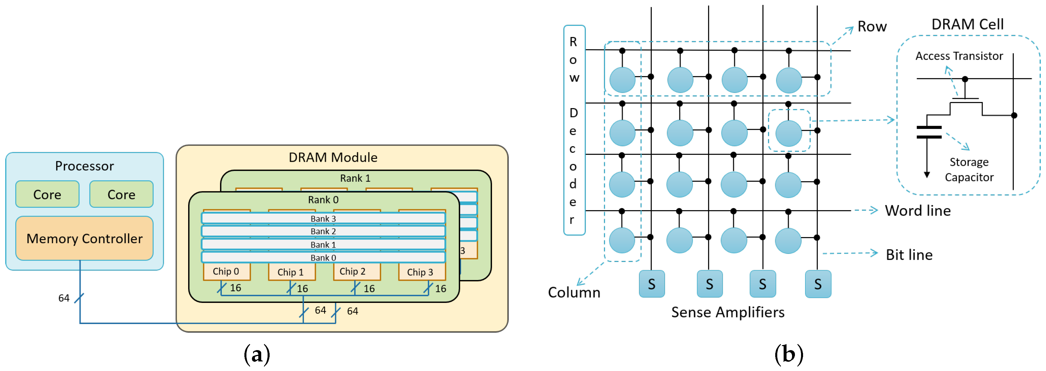
A modern DRAM system is organized into a hierarchy of channel, rank, bank, DRAM chips, DRAM cells, and memory controller, as illustrated in
Figure 1. Memory commands, address space, and data are driven between the memory controller and DRAM modules by the memory channel. Depending on the memory requirement, there might be one or multiple DRAM modules. DRAM modules are divided into one or multiple ranks. A rank consists of several DRAM chips (generally 4/8/16) and provides a wide data-bus (usually 64 bits) together.
To support the parallelism, each DRAM chip consists of multiple banks. In a memory bank, the DRAM cells are placed in a two-dimensional array. The memory address is divided into a row address and column address, which are decoded by a row and a column decoder during a read or write operation to find the corresponding cell. The rows of the DRAM are known as wordlines (or pages). The columns are known as bitlines, and the chip density determines the total number of rows. The bitlines are connected to the row-buffer, which is a row of sense-amplifier. A DRAM cell consists of two components: an access transistor and capacitor to hold a charge. The charging state of the capacitor determines the stored value. The access transistor is used to access the stored value. A fully charged capacitor represents logic ‘1’, and an empty capacitor represents logic ‘0’. The access transistor connects the capacitor with a bitline and is controlled by the wordline. The DRAM content (i.e., the state of charge in the capacitor) is read or overwritten by activating a wordline. A to the wordline makes a path between the capacitor and bitline. The bitlines also connect the DRAM cell to the sense amplifier (i.e., row-buffer).
Initially, in the precharge state, all bitlines are precharged to . In the next state, the wordline is activated by raising the value of the wordline to . Once the pass-transistor of the DRAM cell is ON, the charge flows between the capacitor and the respective bitline. The charge moves from the bitline to the capacitor if the stored value is ‘0’ and vice-versa. In the last stage, the sense-amplifier attached to the bitline amplifies the bitline voltage to strong logic ‘1’ (or ‘0’). Cell data are then read or written by sensing or driving the voltage of the corresponding bitlines. DRAM cells lose data over time as the cell capacitors discharge gradually and need to be replenished periodically. This operation is known as refresh operation, and the time required is the retention time (). The voltage change due to capacitor discharge is known as voltage perturbation. The data stored on the DRAM cell are lost when the sense amplifiers cannot reliably differentiate the perturbation from noise. Traditionally, DRAM cells are required to have a retention time equal to or greater than 64 ms to preserve data integrity. Recall that sense amplifiers drive each bitline fully to or 0 V when a row is activated. Consequently, the activated row’s cell capacitor is fully charged to or 0 V.
2.2. Retention-Based Error
A retention error occurs when a DRAM cell loses its data due to charge leakage in the cell capacitor. The leakage current differs between cells depending on the manufacturing variation of the capacitor and the access transistor [
15]. Studies show that the retention time in DRAM varies following a bi-modal distribution [
16,
17]. Over 99% of the cells in a DRAM chip can hold the data for a much higher retention time (main distribution). The remaining 1% of cells have high leakage current and exhibit a very low retention property (tail distribution). In order to ensure the reliability of the DRAM cells across the whole population, the standard retention time is determined by the leaky cells of the tail distribution as it consists of the weakest cells of the device. Prior studies have introduced mechanisms to profile the cells’ retention time and refresh DRAM cells intelligently to alleviate substantial energy and performance overhead caused by the refresh operations [
15,
18,
19]. These methods accumulate cell retention times into different bins based on varying retention times and apply different refresh rates to different bins in order to avoid unnecessary refresh operations.
2.3. Disturbance Error
Disturbance errors are caused by a strong interaction between two circuit components, such as capacitors and transistors. In [
5], one specific disturbance error is identified as a row-hammer error when the voltage of the wordline is toggled continuously to cause the nearby rows’ weak cell to leak charge at a higher rate. These disturbance errors are attributed to a cumulative interference of different device-level interactions such as electromagnetic coupling, hot-carrier injection, bridge faults, etc. [
5].
2.4. True Cells and Anti-Cells
In DRAM cell architecture, a true cell refers to a cell that is a logical 1 with the charged state and an anti-cell represents a logical 1 with the discharged state [
5]. Typically, DRAM modules comprise a combination of true cells and anti-cells. Consequently, the retention error probability may be applied to true cells and anti-cell regions independently. For the true cells, retention error will occur only when the stored value is ‘1’ and the capacitor is charged. Thus, the capacitor can be leaked in this state and cause a retention error, but no error will occur when the stored value is ‘0’. In contrast, the logic values ‘0’ and ‘1’ are treated as the opposite in the inverted anti-cells. The anti-cells will exhibit a retention error when the stored logic value is ‘0’ and the capacitor is in a charged state. Similarly, no error will occur when a logic value of ‘1’ is stored in the anti-cells.
2.5. Wear-Out Mechanisms in DRAM
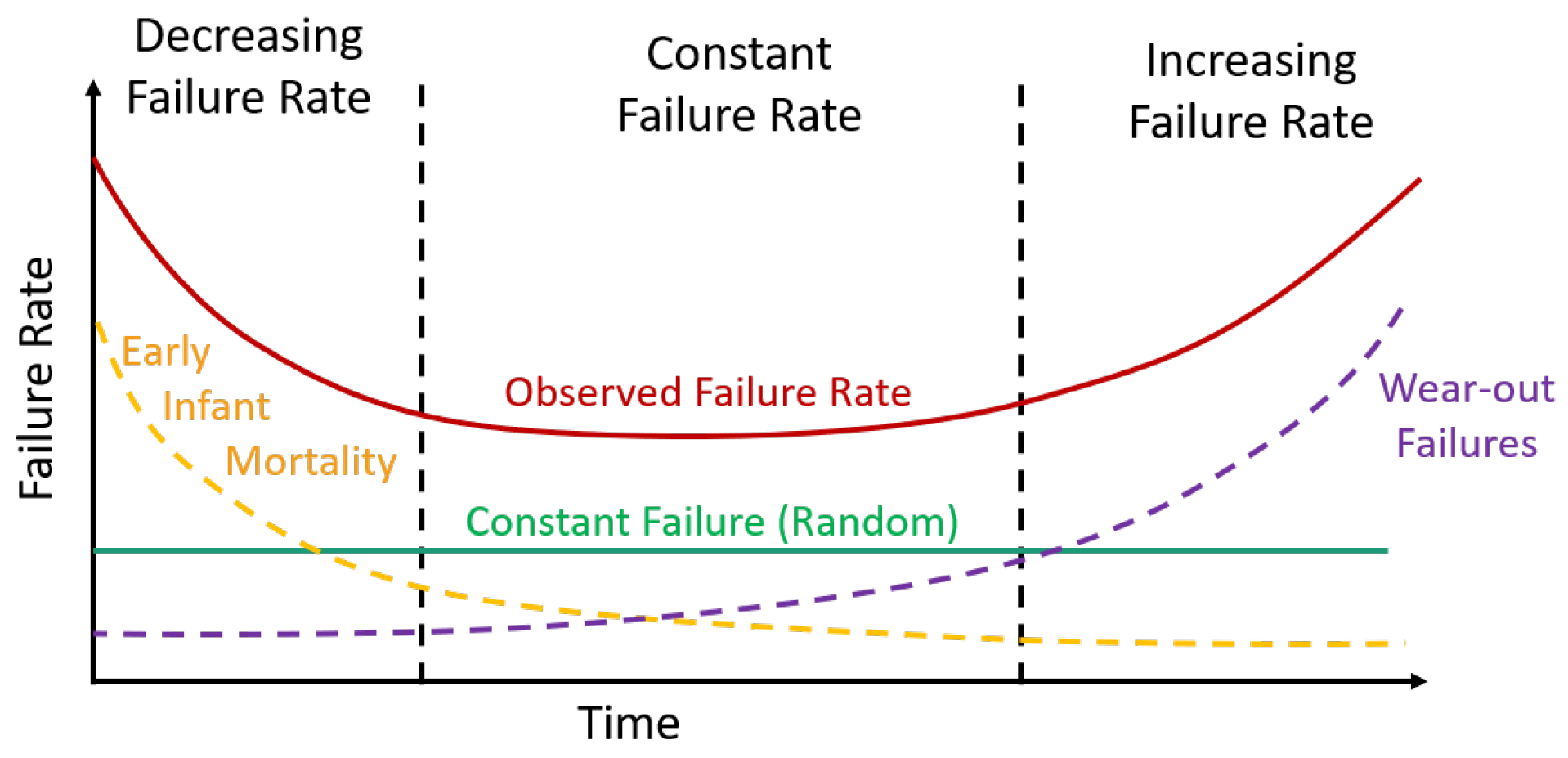
As process technology scales down to smaller nodes aggressively, integrated circuits suffer from increasing performance variation and concerns about the reliability of operation, leading to a fabricated chip’s failure. Failures can occur at various stages in the lifetime of an integrated circuit. ICs can fail during production due to disproportionately high process variations, weak design, or local defects. Electronic devices also suffer from a high failure rate known as infant mortality during the early life in operation [
1]. Integrated circuits can also fail during their lifetime because of wear and tear, aging, harsh environments, overuse, etc.
Figure 2 presents the typical bathtub curve, which is often used to illustrate electronic device failure characteristics [
1].
Recycled or aged electronic devices often exhibit weaker performance and a shorter time to failure. The fundamental wear-out mechanisms are essential to understand the factors influencing transistor and capacitor degradation with aging. Commonly found wear-out failure mechanisms, such as bias temperature instability (BTI), hot carrier injection (HCI), time-dependent dielectric breakdown (TDDB), etc. are discussed in this section.
2.5.1. Bias Temperature Instability (BTI)
Bias Temperature Instability (BTI) is the phenomenon in which the transistor threshold voltage shifts because of the trapped charges at the Si–SiO
2 interface. Dangling bonds at the substrate–oxide interface act as trapped charges, increasing the donor concentration and threshold voltage [
20]. NMOS cell transistors are affected by Positive Bias Temperature Instability (PBTI) when their gate bias voltages are positive. Generally, they experience less BTI impact than PMOS transistors [
10]. The long-term impact of BTI depends on the transistor’s duty factor as the cell transistors are stressed out only during the active mode of DRAM operations.
2.5.2. Hot Carrier Injection (HCI)
HCI is the adverse effect where a charge carrier gains enough kinetic energy and a potential barrier to break from an interface state. The hot carriers create trap states in the gate oxide by breaking the silicon–hydrogen bonds. Most of the degradation occurs near the end of the channel as the charge carriers have high kinetic energy in this region [
21]. The switching characteristics may be permanently altered because of the trapped charge carriers at the gate dielectric. NMOS circuits suffer more from the HCI effect than PMOS circuits as the electrons in the n-type device have a smaller energy barrier than holes in p-type devices.
2.5.3. Time-Dependent Dielectric Breakdown (TDDB)
In the TDDB failure mechanism, the gate oxide breaks down due to a relatively low electric field’s long-time application. When MOSFETs are operated at a voltage close to or beyond their specified operating voltages, trapped charges may form a conducting path through the dielectric gate oxide to the substrate. Defects occupied by electrons or holes will generate a tunneling current through this conductive path once the trap density reaches a threshold point. Thus, it will result in a large current flow through the gate, heating the oxide layer and finally breaking down the dielectric completely [
22].
2.5.4. Radiation Failure
Ionizing radiation from natural or artificial sources may create hundreds of electron–hole pairs in the gate oxide, which can degrade the transistor and even disrupt performance [
23]. The electrons get swept away out of the gate oxide due to high mobility, leaving trapped positive charge at the Si–SiO
2 interface. Consequently, it results in a shift of threshold voltage and increases the channel leakage current [
20,
24]. Over an extended period of time, trapped charges at the interface and oxide may cause the TDDB effect and a complete breakdown of the dielectric oxide.
An integrated circuit’s performance slowly but gradually degrades over time due to such wear-out phenomena. The degradation rate might depend on the switching activity, the gate voltage, the content of the DRAM cell, and several other factors [
25,
26].
3. Testing Methodology
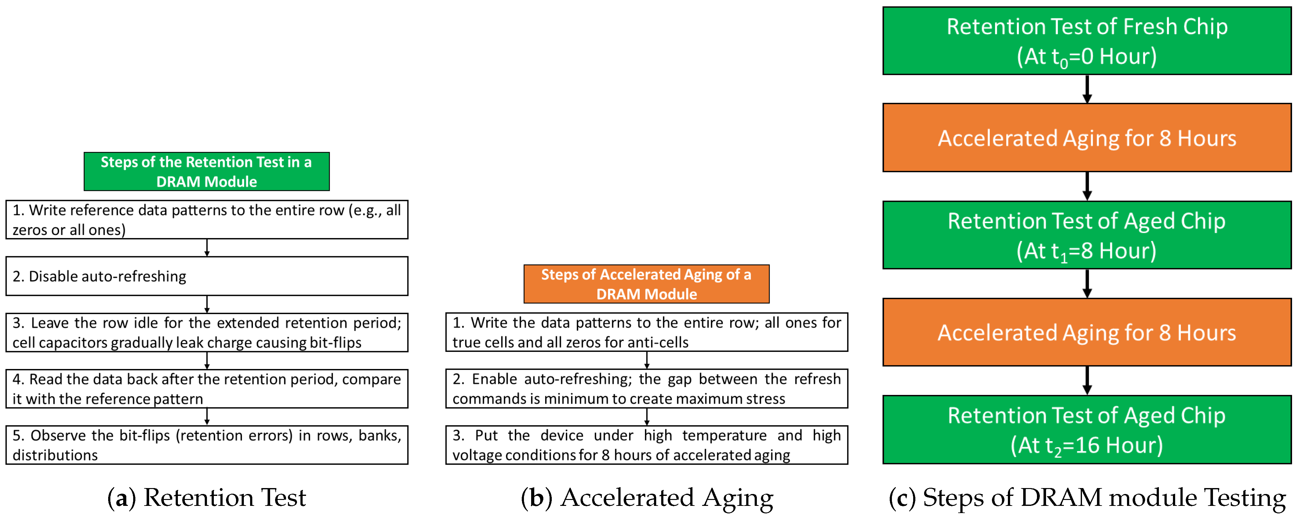
This section presents a brief description of the testing methodology and the steps involved for the experimental study. The testing methodology can be divided into two parts: DRAM retention test and accelerated aging. In a retention test, the cell capacitors in a DRAM module are allowed to leak charge for an extended retention period to induce error in the written data. In accelerated aging, the module is taken through a burn-in test at a high temperature and voltage for a long time. At the stress condition, the wear-out mechanisms affect the cells.
Initially, a DRAM retention test is carried out to analyze the induced errors in the cells at a lower refresh rate for fresh modules. Then, the DRAM module is taken through an accelerated aging process for 8 h. The retention test and accelerated aging process is repeated several times to observe the effects on retention error. In our experiment, the retention error measurement is performed for each bank at three different time points:
h,
h,
h. The tests for the same devices are performed under the same condition to mimic the effects of aging degradation with time. While devices at
are referred to as fresh or brand new, devices at
are presented as aged or recycled or counterfeit devices. Now, the induced retention errors can be compared for the fresh chips and aged chips at two different aging points.
Figure 3 illustrates an overview of the testing methodology and steps required to find the retention-induced error and the effects of accelerated aging.
3.1. DRAM Retention Test
A DRAM retention test is performed by increasing the time to refresh the DRAM cells and observing the errors induced due to cell capacitor leakage. In our experiment, retention-based errors are induced by refreshing the rows with a much higher retention time than the standard retention period of 64 ms. This allows the cell capacitors to leak for an extended period of time, causing bit flips to a significant number of cells. The retention test involves the following steps:
A reference data pattern is written to a complete row. We use all zeros (0x00) and all ones (0xFF) patterns in our experiments.
Auto-refreshing is disabled because we want the cells to leak charge for an extended retention period without being refreshed.
The rows are left idle for the specified retention time (10 s, 20 s, etc.). The cell capacitors gradually leak charge, causing bit flips in the cell data.
The data are read back from the rows after the retention period and sent back to the host machine. The read data are compared with the written data to detect the cells that could not hold the data for that duration as the bits are flipped.
The raw data are analyzed to observe the bit flips/retention errors of a DRAM module in the rows, banks, and their distributions.
These steps are performed for all the rows in a DRAM bank and for all the banks in a module at time. To ensure that only the refresh or retention time affects the cell leakage in this test, we perform the read and write operations with the standard timing parameters. In our experiment, we perform the retention test for three different retention times: at = 10 s, 20 s, 50 s.
3.2. True and Anti-Cell Detection
After collecting and analyzing the new DRAM modules’ retention errors for different patterns and retention times, the errors are attributed to process and architectural variation. From the retention test results, the phenomenon of design-induced variation is observed in two forms: (i) true cells and anti-cells due to architectural variation of the cells and (ii) variation across local parts of the bank due to relative distance from the peripherals [
27]. True cells induce error only for logic ‘1’ as the cell capacitor discharges from HIGH to LOW state, and they do not induce any error for logic ‘0’ as the capacitor remains at the LOW state. On the other hand, anti-cells discharge for logic value ‘0’ and induce error and show no error for logic value ‘1’.
In order to identify the true cells and anti-cells, the follwing steps are required:
The retention test is performed separately with all-zeros (0x00) and all-ones (0xFF) patterns in a module.
The retention errors in bank are aggregated for each row.
The rows that induce error only for the 0xFF pattern and show no error for the 0x00 pattern are identified as true cells. The rows inducing error only for the 0x00 pattern are identified as anti-cells. The rows that show errors for both patterns have a mixture of true and anti-cell configuration.
Identifying true cells and anti-cells is important for the aging process. In the aging process, our goal is ensure maximum stress to the storage capacitors. In order to achieve that, data pattern 0xFF is written to the true cells and pattern 0x00 is written to the anti-cells to ensure uniform aging across the DRAM array. In the modules with a mixture of both true cells and anti-cells, the 0xFF pattern is written to all the rows during the aging process.
3.3. Accelerated Aging of DRAM Modules
In order to observe the wear-out effects on the DRAM chips, a test similar to the burn-in test is performed on the DRAM modules. The module is exposed at an elevated temperate and DC voltage for a prolonged period of time to simulate a stress condition. This stress condition accelerates the aging process in the cell transistors. When DC stress is applied to the DRAM node, the leakage current increases due to trapped emission electrons, and the DRAM cell capacitors suffer from asymmetric damage, degrading the retention behavior [
28]. Evaluating the retention error at this accelerated aging condition can be used to identify the impacts of wear-out mechanisms (e.g., BTI, HCI, electromigration) and detect the aged device as well as the infant mortality failures and unexpected failures [
2].
The following steps are involved in the accelerated aging process:
Initially, a data pattern is written to the entire row using standard timing parameters. In order to ensure maximum stress, all ones (0xFF) are written to the true cells, and all zeros (0x00) are written to the anti-cells.
Auto-refresh is enabled. The timing parameter (the gap between refresh command) is set to 0, a minimum value (one clock cycle), so that DRAM cells are refreshed more frequently and create maximum stress on the storage capacitor.
The DRAM module is placed under the thermostream device at a high temperature of 70 °C and a high-voltage condition ( 1.55 V instead of standard 1.5 V. At this stressed condition, wear-out effects are accelerated in the DRAM cells. The module is left in this condition for 8 h for wear-out mechanisms to affect the DRAM cells.
After the aging process in stress conditions, the module is cooled down to room temperature, and the retention test is performed to evaluate the bit flips. The retention errors are compared with the fresh chips and the additional errors are attributed to various aging mechanisms.
4. Experimental Results and Analysis
We describe the experimental framework and retention test results for the fresh and aged DRAM modules in this section. We observe the retention test results for new modules and determine how the number of retention errors in DRAM modules varies depending on the data pattern, timing parameter, and architectural variation. Then, we observe the retention results of the aged modules to characterize the effects of wear-out mechanisms.
4.1. Experimental Framework
A DRAM testing framework based on Xilinx ML605 FPGA, and a DDR3 memory controller called SoftMC [
29] is used to test the DDR3 modules in our experiments. Retention error data are collected from nine commercially available off-the-shelf single rank DDR3 SODIMMs modules (small outline dual in-line memory module) covering all three major DRAM vendors. We used a Micron 1 GB DDR3 module, Hynix 2 GB module, and Samsung 2 GB modules in our tests. Each memory module contains four or eight ICs with eight banks spreading across the whole module, and each bank consists of 16 k or 32 k rows (1 GB or 2 GB).
SoftMC is an FPGA-based open-source experimental memory testing infrastructure that implements all low-level DRAM commands in a programmable memory controller. This programmable memory controller is introduced to the user with an easy-to-use and flexible interface. This interface can be programmed in C++ with customized library files to generate bit files. The user can generate a sequence of DDR3 operations by calling the SoftMC API functions [
29]. DRAM cell data can be written or read from each memory bank using the testing platform implemented on a Xilinx Virtex ML605 evaluation board with SoftMC.
The experimental framework provides the ability to:
Generate different timing parameters and test patterns for various latency-based tests of the DRAM module.
Facilitate with an interface to connect the host machine with the Xilinx FPGA board.
Enable precise and accurate control of the temperature of the DRAM module during the test.
In order to sustain a stable operating temperature for the DIMMs during the DRAM aging process, the modules are placed on the FPGA board under an ATS Series Thermostream device [
30]. The Thermostream device allows for fast and precise thermal conditioning with a temperature range of −20 to +225 °C.
4.2. Retention Error in Fresh DRAM Modules
For standard DRAM operations, each row is refreshed periodically after 64 ms. If the DRAM cell capacitors are refreshed after a longer interval, the cells lose charges and cause a bit flip. The number of retention errors for a fresh DRAM module depends on the retention time, data pattern, and architectural variations.
4.2.1. Dependence on Retention Time
Since the standard retention time is chosen with a high reliability margin [
16], the number of retention errors is nonexistent or very few in a retention test with standard retention time. In our experiment, we increase the retention time to
= 10 s, 20 s, and 50 s to induce a significant number of bit flips in the cells. We observe that the number of erroneous cells increases by over 100 times when the
is increased from 10 to 20 s and by over 1000 times when the retention time is increased to 50 s, as shown in
Table 1. It is the extreme case scenario, as
values are picked carefully from hands-on experience to result in the maximum transition in the number of retention errors. However, it is expected to see a sharp increase in error at higher retention times as more and more cells lose their charge due to increased leakage.
4.2.2. Dependence on Data Patterns
We collected retention data for the fixed patterns 0x00 and 0xFF, as previous work suggests that this testing is sufficient [
31]. Consecutive alternate bits of 1 and 0 (checkerboard patterns) increase the coupling noise with a voltage difference between the neighboring bitlines, which may induce the worst-case data pattern [
31].
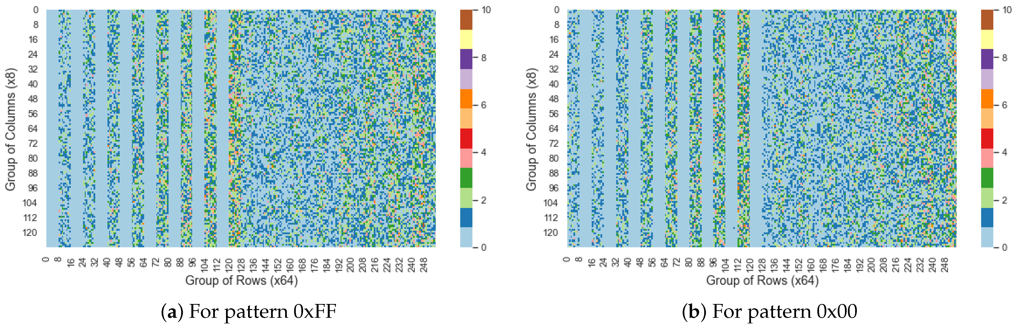
From the retention error results for 0x00 and 0xFF, the true cells and anti-cells can be identified.
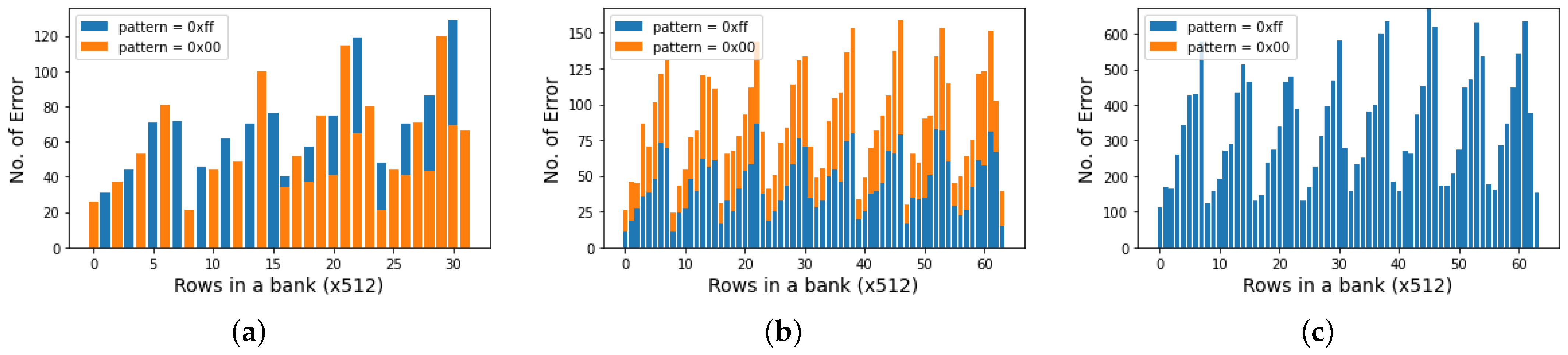
Figure 4a,b present the heatmap of retention errors across the rows and columns in a Micron module for patterns 0xFF and 0x00. The x-axis represents the 16,384 rows divided into 256 groups and the y-axis represents 1024 columns divided into 128 groups. Aggregated number of errors for 64 consecutive rows and 8 columns is represented by each color-coded block. We observe the number of errors increase from left to right, and there are intermittent gaps after every 512 rows. This can be explained by the true and anti-cell architecture of the module. Some rows show a retention error for the 0xFF pattern but not for the 0x00 pattern, which are identified as the true cells. Similarly, the rows that induce error only for pattern 0x00 are identified as anti-cells. The rows that induce error for both cases have a mixture of true-cell and anti-cell architecture.
4.2.3. Design-Induced Variations
There exists variation in access latency among different regions in a DRAM chip due to the relative distances of different components from the peripheral structures. Cells located closer to the sense amplifiers can be accessed faster as they experience smaller RC delays [
27]. Design-induced variation is static and depends on the physical organization, i.e., it is always determined by the cell’s location. DRAMs with the same internal design demonstrate a similar pattern in failure distribution [
27].
In
Figure 5, we observe the design-induced variation for different DRAM vendors. The x-axis represents the bins of row numbers where every 512 consecutive rows are grouped together. The y-axis represents the aggregated number of bit flips in a group of 512 consecutive rows for patterns 0xFF and 0x00. We observe that the number of failures in the rows gradually increases with increased distance from the peripherals, and this pattern periodically repeats. In addition, the design-induced variation pattern repeats every 4096 pages (eight groups of 512 pages). The repetition is caused by the introduction of a new global sense amplifier and completely dependent on a specific array architecture. We observe two different regions in the Micron design, which is explained in detail in
Section 4.2.4.
4.2.4. Impact of True Cells and Anti-Cells
We observe the impact of previously discussed architectural variation as true cell and anti-cell for Micron and Hynix DRAM modules in
Figure 5a,b. For the Micron 1 GB module, we observe two different architectural variations inside a bank. Each bank consists of 16,000 rows or pages, and each page holds 1000 columns, each with a 64 bit length. We observe a spatial locality of 512 pages in the first half of the bank. In this portion, the first 512 pages induce error for pattern 0x00 and are characterized as anti-cells, and the next 512 consecutive pages are characterized as true cells. On the second half of the pages, we could not find any large-scale granularity, which means that either one or very few consecutive pages are true cells or the next page or a few are anti-cells. On a different note, one or more individual bits in a column could be true cells, and the next one or more could be anti-cells, which is the most likely case to maintain uniformity across the 3D stack of a DDR3 memory module. The Hynix module follows the same architecture as the second half of the Micron module across the whole module (
Figure 5b).
Figure 5c illustrates the retention error across rows in the case of the Samsung modules. It shows that all the cells are designed with true cells, which explains the errors found only for data pattern 0xFF.
4.3. Aging Effects on Retention Error
From the silicon results, we find that the retention errors are vulnerable to aging; as the devices age, retention errors increase. We present the summary of total retention error and their pattern dependency, retention time dependency, and the impact of accelerated aging for sample DRAM modules from three different vendors in
Table 1. The noteworthy observations from the experimental results are highlighted below.
4.3.1. Increase in Retention Error with Aging
The number of total erroneous cells (retention errors) for all three different retention times (
10 s, 20 s, 50 s) increases drastically as the devices age (
Table 1). We observe about a 5–10% increase in retention error after 8 h of aging and about 15–30% after 16 h of aging for Micron and Hynix DDR3 modules. When deployed in the field for several months or years, the change in retention error will be significant enough to distinguish an aged module from a new one. In the case of the Samsung modules, we observe a deviation of aging behavior as very few errors are induced for data pattern 0x00 because of design variation. The errors induced for data pattern 0xFF are clustered in a few rows and decrease with aging. In this case, the design-induced variations dominate over aging impacts.
Moreover, for our chosen data patterns, we observe that the 0x00 pattern induces a slightly higher retention error than the 0xFF pattern, as shown in
Table 1. Even though there are some variations in retention error due to input patterns, they are in the same range, which illustrates that the number of true cells and anti-cells is almost equal in Micron and Hynix manufactured DRAM chips. On the other hand, the Samsung modules do not show any error for the input pattern 0x00, which indicates that the Samsung chips do not have the architecture of true cells and anti-cells; instead, all the cells are designed following the same true-cell architecture.
4.3.2. Error Distribution with Aging
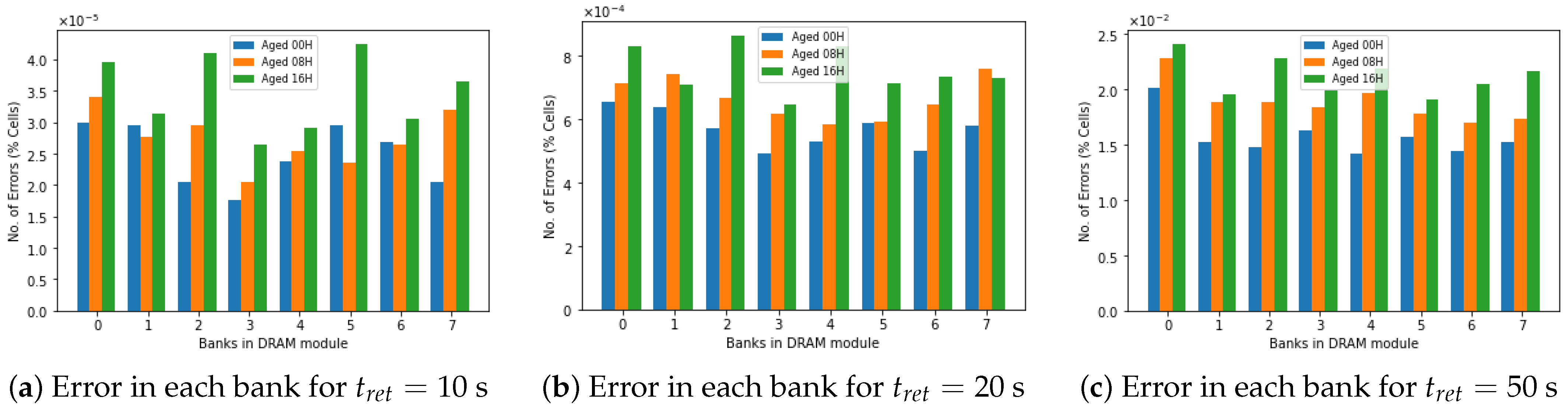
In order to illustrate the aging effects on the retention behavior of DRAM modules, we explore the distribution of error across the banks and group of rows.
Figure 6 illustrates the retention errors for pattern 0x00 in each bank of a Hynix 2 GB DRAM module and their corresponding distribution curve. In
Figure 6a–c, the number of total retention errors across the banks is plotted at three aging points. We observe that the total retention errors in each bank increases consistently with aging as the wear-out effects occur. This phenomena is consistent for different retention times, as shown in
Figure 6a–c.
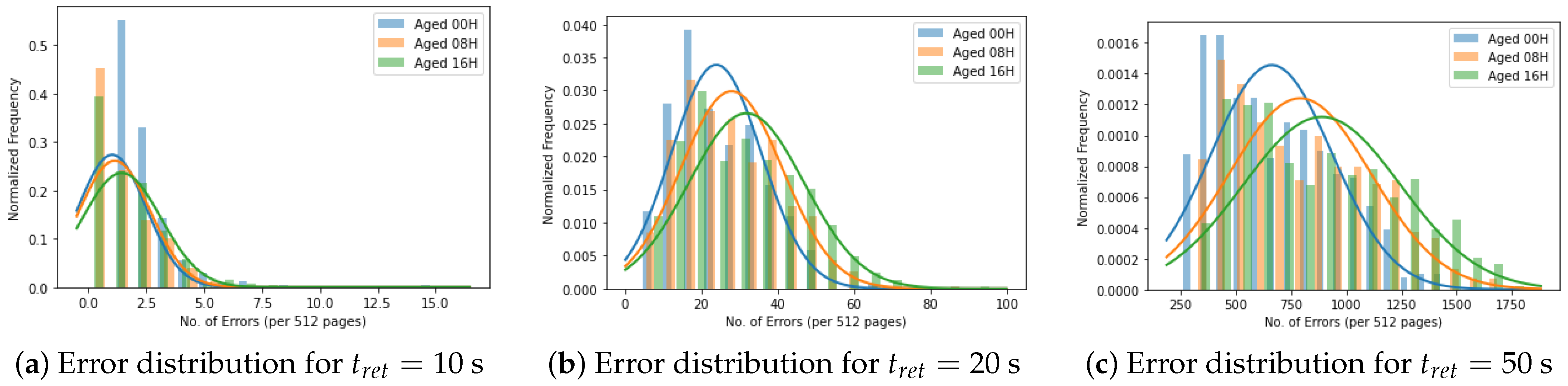
Retention errors for consecutive 512 rows are aggregated in a group in order to observe the changes across the rows.
Figure 7a–c show the histogram and the approximate normal distribution curve of errors in a group of rows. Additionally,
Table 2 presents the corresponding mean and standard deviation of the retention error distribution curves. We observe that as the device ages, the mean of the distribution curve shifts rightward. Moreover, the standard deviation of the distribution increases as the variation in total errors in a row across the bank is higher as the device ages. In these figures, we notice that the error distribution of higher retention times is more useful as they induce a high number of errors, and the difference between the new and aged/recycled modules is very evident. These retention-based signatures can be utilized to observe the evidence of device aging and classify the recycled devices by comparing them with the signatures of a new device.
6. Conclusions
This paper presents an experimental study to characterize DRAM aging behavior by analyzing the retention error. From real-time silicon measurements of DRAM devices from multiple vendors, it is concluded that retention-based error can be used as an effective device signature to observe aging effects in DRAM cells. The architectural variation results in true-cell and anti-cell configurations among cells in a DRAM module. These variations can be utilized to speed up the aging process by a factor of two. There are other design-induced variations, such as local variations among pages in a bank that depend on the distance of the cells from the peripheral structures. A considerable increase in retention error and a shift in the distribution curve are found with accelerated aging. It is concluded that an extensive study of the error statistics can be used to classify recycled chips with a threshold value of the average increase in retention error. However, the recycled DRAM detection is challenging because of the slow aging process of DRAM cells and a lack of available resources on the specifications of the modules available. The DRAM memory controller is also limited in many aspects because DDR4, and higher generations of modules, cannot be tested with the platform. Moreover, the testing process is very time consuming, and many memory modules working in the field do not behave as expected from the literature. In the future, the findings of this research can be utilized to develop an independent, non-invasive method to detect recycled DRAM chips without any additional circuitry or cost. The impacts of individual aging mechanisms can be evaluated, and the inconsistent behavior of a few DRAM modules can be explained with the reliability prediction model.


