1. Introduction
The piezotronic and piezo-phototronic effects of non-centrosymmetric semiconductors, such as ZnO, GaN, and InN, have received tremendous attention because of their ability to enhance the electrical and optoelectrical performance of devices, such as field-effect transistors, photodetectors, light-emitting diodes, and solar cells [
1,
2,
3,
4,
5,
6]. To date, among the non-centrosymmetric wurtzite semiconductors, ZnO has been regarded as the most potential candidate owing to its attractive advantages: facile preparation for a variety of nanostructures with different shapes, outstanding semiconducting characteristics, [
7,
8] and the ease of hybridization with other materials to utilize its extraordinary physical properties in various applications [
9,
10]. In particular, a one-dimensional (1D) ZnO NW array architecture, compared to single-nanowire (NW)-based devices and 2D thin films, exhibits additional advantages because of its ability to withstand a relatively large external mechanical strain within a large surface area, its excellent multichannel charge transport, and its enhanced light absorption [
11,
12,
13,
14].
Nonetheless, the presence of a large number of surface states within ZnO NWs limits the performance of electronic and optoelectronic devices, and it affects their stability [
12,
15]. Accordingly, to improve the performance of ZnO NW arrays, surface and/or interface modification engineering has been proposed as an effective strategy, such as the fabrication of core/shell NWs by the deposition of a shell layer on the ZnO NWs [
16,
17,
18,
19].
Among various composite structures for ZnO-based core/shell NWs, a heterojunction with a type-II band alignment, where the valence and conduction band of the ZnO core are lower than those of the shell, can separate the electrons and holes into different spatial regions [
16,
17,
20]. This type-II core/shell structure not only enables the reduced surface states of the intrinsic ZnO core but also improves the charge carrier transport caused by the spatial separation of electrons and holes in different conducting channels. Thus, numerous studies have reported the application of a type-II band structure to various optoelectronic devices by coating the ZnO NW array with shells, such as ZnS, ZnSe, and CdS [
20,
21,
22,
23]. Above all, the type-II band alignment of ZnO/ZnS core/shell NWs has become the focus of intensive research with respect to the fast separation of photogenerated carriers due to the remarkable application potential for not only photovoltaic devices but also solar-driven photoelectrochemical water splitting, photocatalytic hydrogen production, and gas sensors [
24,
25,
26,
27].
To date, by applying external strain to various core/shell NWs with such a unique type-II band structure, numerous studies have reported on the piezotronic, piezo-phototronic, and piezo-photocatalytic effects [
28,
29]. Related core/shell NW devices have emerged for a broad range of applications, producing eco-friendly hydrogen fuel or detecting different sources in the environment, such as human motion/pressure and light. However, an in-depth discussion of the influence of the piezoelectric and piezo-phototronic effect of these NWs on the performance of each device through the quantitative calculation of Schottky barrier height (SBH) changes has not been reported. The core of piezotronics and piezo-phototronics is based on the use of the strain-induced piezoelectric potential generated inside non-centrosymmetric semiconductors that are in contact with the metal contact interface [
30]. Therefore, it is essential to understand how the strain-induced piezoelectric potential affects the SBH of the devices and how it modulates the charge transport, separation, and recombination processes at the junction.
Here, we fabricated ZnO and ZnO/ZnS core/shell NWs and evaluated the electrical and optoelectrical properties of these two devices on flexible substrates under applied external strain and under UV irradiation. In addition, we compared the dependence of SBH changes and the strain of the ZnO/ZnS core/shell NWs and ZnO NWs to understand the physical modulation mechanism of the two- and three-way coupling of piezoelectric, semiconducting, and optical excitation properties.
2. Results and Discussion
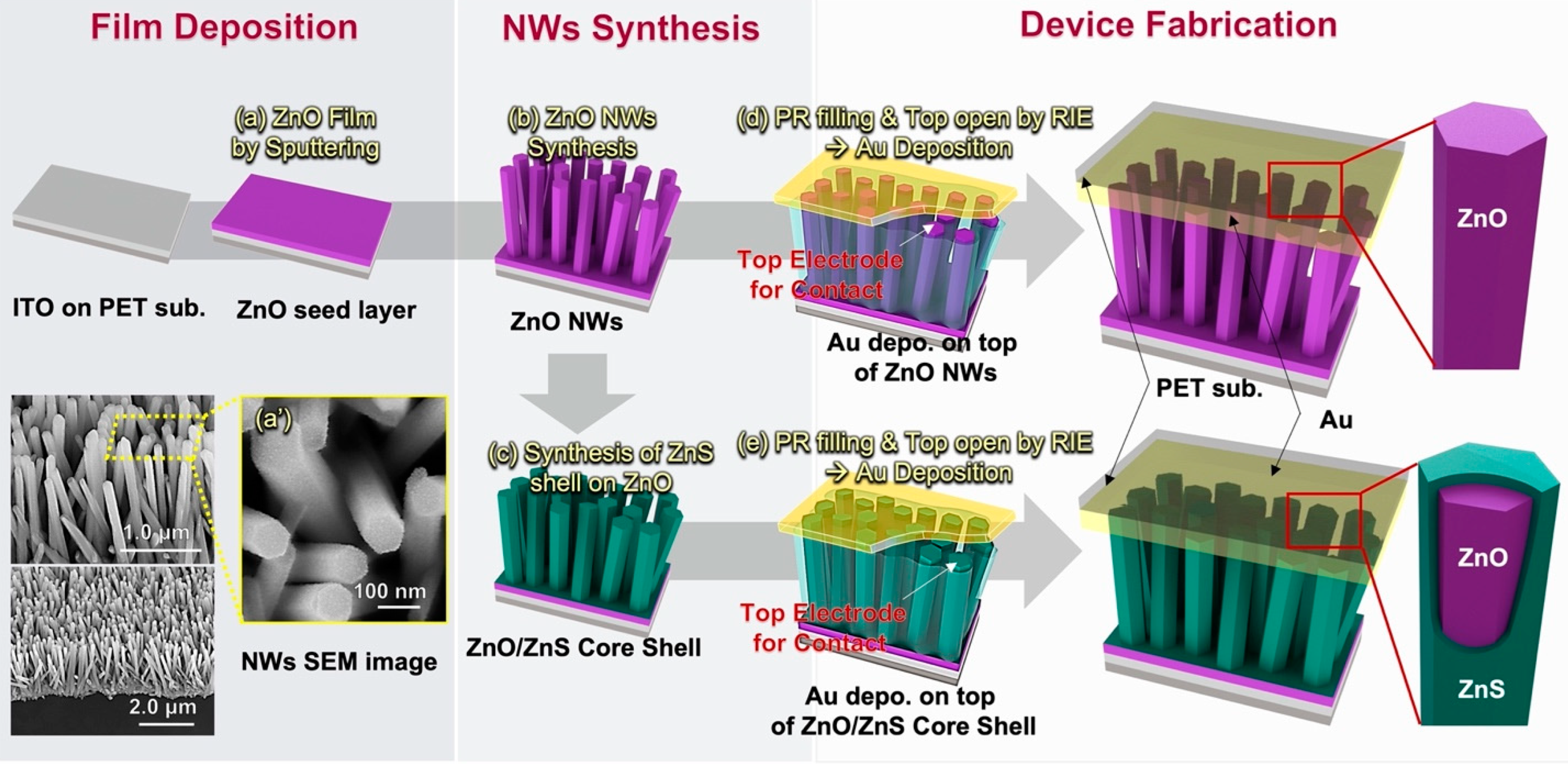
Figure 1 shows a schematic image of the fabrication process of the ZnO and ZnO/ZnS core/shell NW devices. For the fabrication, first, we deposited a ZnO seed layer on a flexible poly(ethylene terephthalate) (PET) substrate with indium tin oxide (ITO) as the bottom electrode using radio-frequency magnetron sputtering (
Figure 1a). Subsequently, the ZnO NWs were grown using a hydrothermal method by dipping the substrate into a solution of zinc nitrate hexahydrate (Zn(NO
3)
2·6H
2O) and hexamethylenetetramine ((CH
2)
6N
4) with a concentration of 0.25 mol/L at 95 °C for 2 h (
Figure 1b). The tilted cross-sectional and top-view field-emission scanning electron microscope (FESEM) images and the low-magnification bright-field and high-resolution transmission electron microscope (TEM) images of the vertically grown ZnO NWs with a diameter of about 50~100 nm are shown in
Figure 1a′ and
Figure S1, respectively.
Thereafter, the ZnS shell was then deposited by immersing the ZnO NWs grown on the substrate in a 0.1 M thioacetamide solution at 90 °C for 50 min (
Figure 1c). To apply strain to the NWs more effectively and to prevent the fracture of the NWs, the NWs were coated with an AZ1512 photoresist film using a spin-coating method. The top layer of the photoresist film was opened using reactive ion etch (RIE) processing, and Au was deposited as the top electrode via e-beam evaporation (
Figure 1d).
Figure S2 in Supporting Information shows the exposed tips of the polymer-embedded ZnO NW arrays depending on the RIE processing time. Lastly, PET film was positioned on the top of the NW arrays to ensure optimal compression under applied strain. These facile and simple synthesis methods at low processing temperatures enable the use of flexible substrates for the fabrication of devices. The details of the complete fabrication process can be found in the Experimental Section.
Figure 2a,b show the tilted FESEM images of the as-grown ZnO and ZnO/ZnS core/shell NWs on the ITO-coated PET substrate, and their corresponding illustrations are schematically shown in the inset of
Figure 2a,b, respectively. Most of the ZnO NWs with rational density exhibited a regular hexagonal shape with a smooth surface, whereas the ZnS shell deposited on the tips of the ZnO/ZnS core/shell NWs exhibited a slightly rough surface after the hydrothermal deposition of ZnS.
To investigate the structure and composition of the ZnO/ZnS core/shell NWs, we performed the high-angle annular dark field scanning transmission electron microscope energy-dispersive X-ray spectroscopy (HAADF STEM-EDS) analysis.
Figure 2c shows the compositional maps collected from the white-boxed area of the HAADF STEM image for Zn, S, and O elements. The core/shell elemental distribution results revealed that a relatively high concentration of S was present at the edge of the NW compared to the core region, confirming the successful synthesis of ZnO/ZnS core/shell NWs.
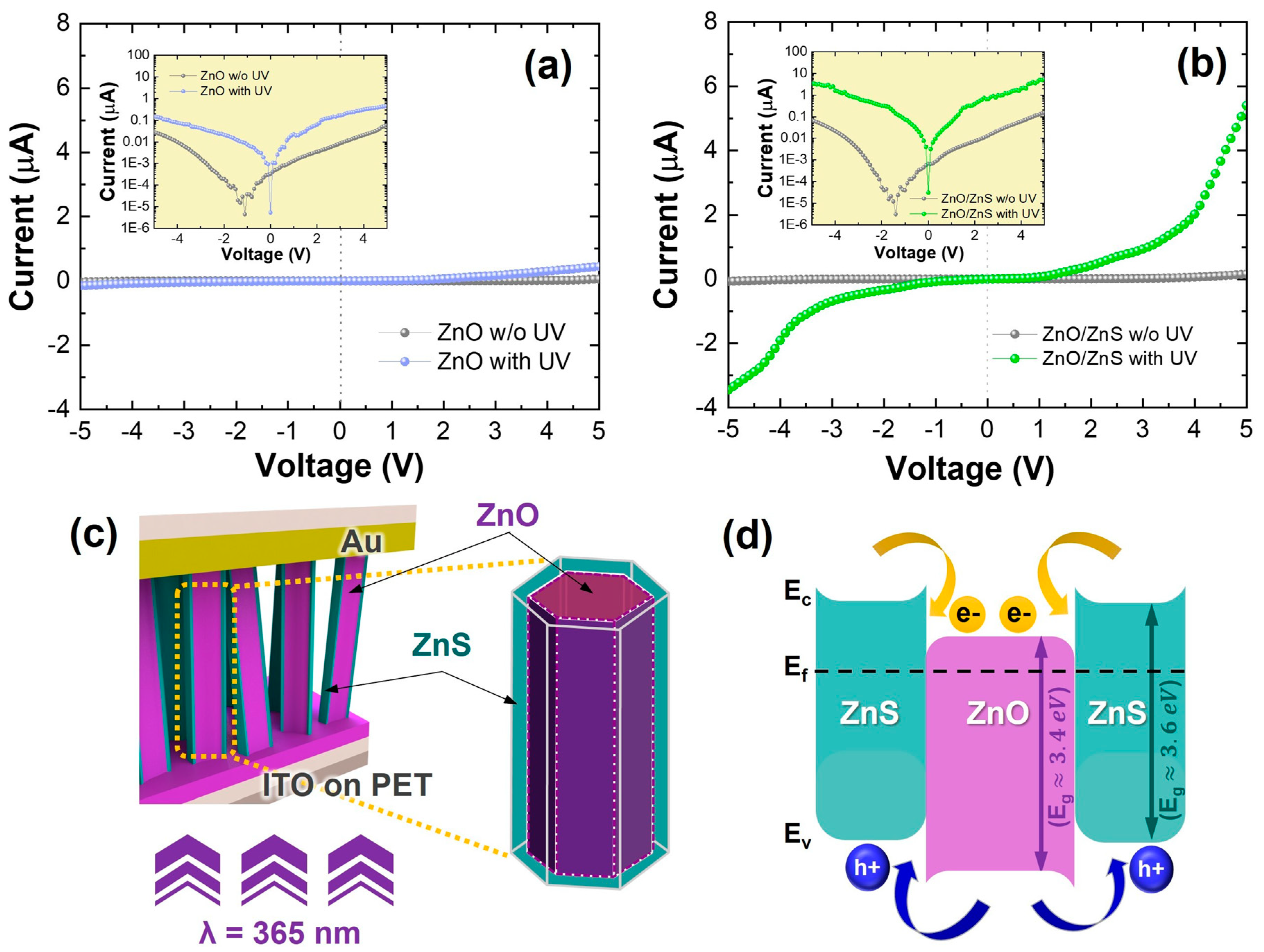
The performance of the ZnO and ZnO/ZnS core/shell NWs under UV illumination is shown in
Figure 3.
Figure 3a,b show the current–voltage (
I–
V) curves of the vertically grown ZnO and ZnO/ZnS core/shell NWs in the dark and under UV LED illumination (365 nm) with a light intensity of 0.78 mW/cm
2. It is important to note that ln
I is linearly correlated with
V in the intermediate bias range for both positive and negative currents under dark and illumination conditions, as shown in the inset of
Figure 3a,b, which corresponds to the typical
I–V characteristic of a back-to-back Schottky barrier structure [
31].
After the devices were irradiated with a UV light of 365 nm from the bottom of the device, as illustrated in
Figure 3c, the photocurrents of both devices increased. For example, at an applied voltage of 5 V, the dark current and photocurrent of the ZnO NWs were 58.4 nA and 0.45 µA, respectively, whereas those of the ZnO/ZnS core/shell NW arrays were 154 nA and 5.4 µA, respectively. This indicates that the photocurrent of the ZnO/ZnS core/shell NWs was 35 times larger than the dark current, whereas the photocurrent of the ZnO NWs was 8 times larger than the dark current, implying that the photoconductivity of the ZnO NWs can be significantly enhanced by forming a shell layer on the core NWs.
The larger enhancement in the output current of the ZnO/ZnS core/shell NWs compared to that of the ZnO NWs can be ascribed to the type-II band alignment of the ZnO/ZnS core/shell NWs, as shown in
Figure 3d. It is well known that a number of surface states exist on the surface of ZnO NWs, facilitating the recombination of the photogenerated electrons with the photogenerated holes [
12]. By coating ZnO NWs with a ZnS shell to form a core/shell structure, the surface state density of the NWs can be modified, and the charge separation of the photogenerated electrons and holes can occur owing to the formation of the type-II band alignment. The type-II band induced the spatial separation and confinement of electrons and holes into the ZnO core and ZnS shell, respectively, and it suppressed the recombination of photogenerated electron–hole pairs under UV illumination [
17]. Hence, the charge carriers contributing to the photocurrent in the ZnO/ZnS core/shell NWs were significantly higher than those in the ZnO NWs. Furthermore, the type-II band alignment enabled the generation of electron–hole pairs not only via the direct band-to-band absorption in ZnO but also via the indirect type-II transition from the valence band maximum of ZnS to the conduction band minimum of ZnO under UV irradiation, which is a wavelength below the bandgap of ZnS, thus resulting in the enhanced photocurrent.
To compare the piezotronic and piezo-phototronic effects of the ZnO and ZnO/ZnS core/shell NW devices, the current–voltage (
I–
V) curves were systematically measured by applying external compressive strains under a UV illumination with a wavelength of 365 nm with a power intensity of 0.78 mW/cm
2. With an increase in the applied external compressive strain from 0 to −0.15%, the output current of both the ZnO and ZnO/Zns core/shell NWs increased cumulatively (
Figure 4a,b).
In particular, the change in the output current with a change in the compressive strain plotted (
Figure 4c,d) indicates that the increase in the current levels of the ZnO/ZnS core/shell NWs (red dots) was higher than that in the current levels of the ZnO NWs (magenta dots) when increasing the compressive strain at biases of −5 V and 5 V. To compare the output currents of the ZnO and ZnO/ZnS core/shell NWs under external compressive strain, we calculated the relative increase in the output current, defined as
, where
Istrain and
I0 are the current with and without a certain external strain, respectively [
32]. The
/
value of the ZnO/ZnS core/shell NWs under a compressive strain of −0.15% at 5 V was 91.1%, whereas that of the ZnO NWs was 42.7% under the same condition. These results can be attributed to the distribution of electrons and holes arising from the type-II band structure of the ZnO/ZnS core/shell NWs, as well as the piezopotential changes across the junction interfaces. Generally, the piezopotential is generated in ZnO NWs when external strain is applied by bending the substrate. In the case of the ZnO/ZnS core/shell NWs, changes in the piezopotential caused by the application of strain can modulate the charge transport across the junction interface not only between ZnO NWs and electrodes but also at the heterojunction interface between the ZnO core and the ZnS shell. That is, electrons in ZnO/ZnS core/shell NWs can be transported more easily owing to the synergy effect of charge separation caused by the type-II band alignment, as well as the piezopotential changes at the heterojunction interface of core/shell NWs by external strain.
To further investigate the piezo-phototronic effect in the ZnO and ZnO/ZnS core/shell NW devices, we measured the strain-dependent photocurrent of both devices under UV illumination (365 nm and 0.78 mW/cm
2). Compared with the
I–
V curves under the dark condition, the
I–
V curves under UV irradiation revealed that the photocurrents of both devices increased with an increase in the external compressive strain in a range from 0 to −0.15% (
Figure 4a,b).
At applied voltages of −5 V and 5 V, the photocurrents of the ZnO/ZnS core/shell NWs (−21.3 µA and 68.4 µA) under a compressive strain of −0.15% were 2.47 and 4.53 times higher than those of the ZnO NWs (−8.63 µA and 15.1 µA) (
Figure 4c,d). To compare the performance of both ZnO NWs and ZnO/ZnS core/shell NWs as a photodetector, we calculated the responsivity and external quantum efficiency (EQE) of the devices under varying compressive strains using previously reported equations [
21]. The responsivity and EQE of the ZnO/ZnS core/shell NWs under −0.15% of compressive strain at 5 V were 1.95 A/W and 6.65%, respectively, whereas those of the ZnO NWs under the same conditions were 0.4 A/W and 1.44%, respectively. The higher photoresponsivity and EQE values of the ZnO/ZnS core/shell NWs compared to those of the ZnO NWs under compressive strain were attributed to the separation of the photogenerated charge carriers due to the type-II band alignment, as well as strain-induced piezopolarization charges at the junction interfaces. These piezoelectric charges can effectively modulate the barrier height at the junction between ZnO NWs and the metal electrode, and they can induce the enhanced transport of photogenerated electrons and holes and a reduced recombination probability for the charge carriers. These results verify that the ZnO/ZnS core/shell NWs exhibited excellent optical sensing properties with more than a 4-fold increase in the absolute photocurrent and responsivity under external compressive strain owing to the piezo-phototronic effect and their type-II band structure.
Furthermore, we calculated the relative increase in the photocurrent under an external strain condition, defined as
, where
Ip,s and
Ip,0 are the photocurrent (indicated by subscript “
p”) with and without a certain external strain under UV light, respectively. The
values of the ZnO/ZnS core/shell NWs and ZnO NWs under a compressive strain of −0.15% at 5 V were 11.7 and 32.3%, respectively. In addition, the
values were lower than the
/
values without UV irradiation. These results can be understood as a piezoelectric screening effect, wherein the piezopotential generated in the NWs wanes owing to the photogenerated charge carriers [
33]. In particular, in the case of the ZnO/ZnS core/shell NWs, we can infer that the piezoelectric screening effect was further increased under UV illumination owing to the type-II band alignment. Thus, while the absolute photocurrent of the ZnO/ZnS core/shell NWs was 4.5 times higher than that of the ZnO NWs, the relative increase in the ZnO/ZnS core/shell NWs by strain was smaller than that in the ZnO NWs.
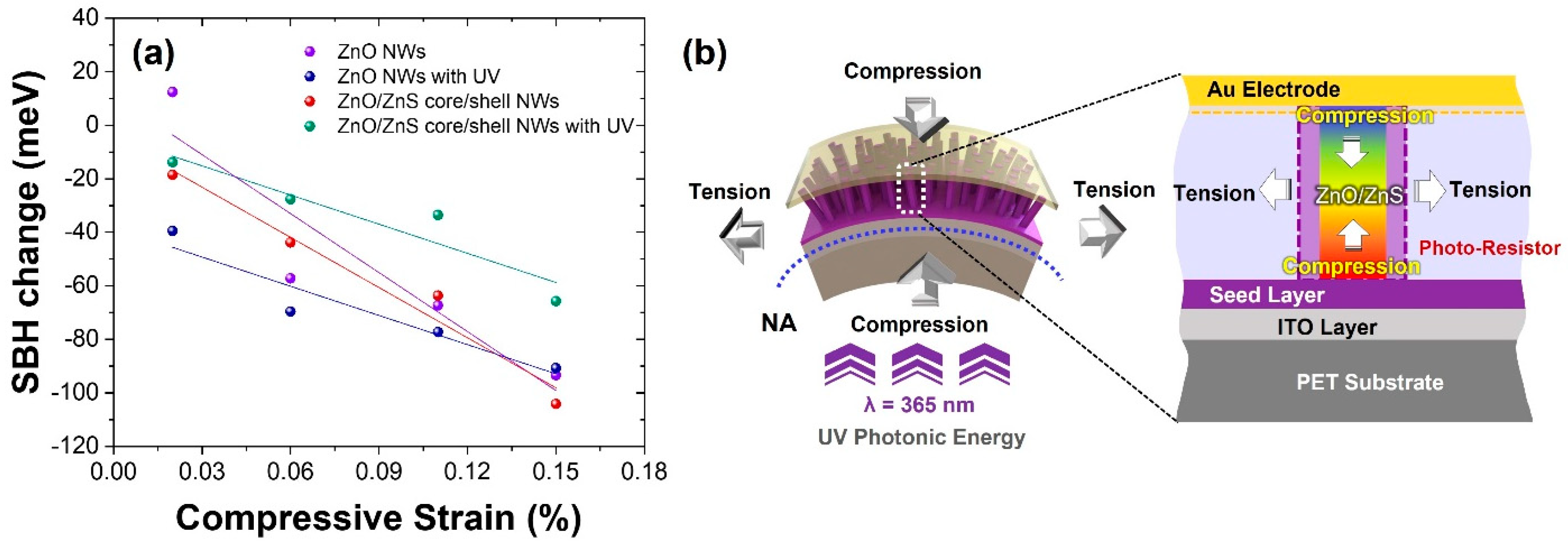
To further understand the physical modulation mechanism, we derived the piezo-induced Schottky barrier height (
SBH) changes from the
I–
V curves using the classic Schottky formular ΔSBH = −
kTln(
Istrain/
Ifree) [
34,
35].
Figure 5a reveals that the calculated
SBH was linearly correlated with the applied strain, indicating that the strain-induced piezopotential can effectively modulate the SBH. When the substrate was bent into a convex configuration by mechanical deformation, as shown in the schematic in
Figure 5b, compressive strain was applied in the growth direction of the
c-axis of the ZnO NWs. Consequently, the NWs undergoing stress generated a piezoelectric potential difference along the ZnO NWs under axial strain, and this localized piezopotential modified the SBH at the metal–junction interfaces, thus adjusting the charge transport and separation at the interface through piezotronic and piezo-phototronic effects under UV irradiation [
32].
As shown in
Figure 5a, the obtained
SBH of both ZnO NWs and ZnO/ZnS core/shell NWs increases monotonously with an increase in the external compressive strain from 0 to −0.15%. These results demonstrate that positive piezoelectric polarization charges were generated at the interface of Schottky contact and that they can effectively reduce the Schottky barrier, resulting in an increase in the current flow. In particular, it was observed that the
SBH slope of both devices under UV irradiation decreased compared to that under the dark condition, which could be attributed to the reduction in the piezopotential generated in the ZnO NWs by the screening effect of the photogenerated charge carriers [
34]. In addition, although the
SBH slopes of the ZnO NWs and the ZnO/ZnS core/shell NWs under UV irradiation were similar, we observed a significant increase in the absolute photocurrent of the ZnO/ZnS core/shell NWs with an increase in the applied strain.
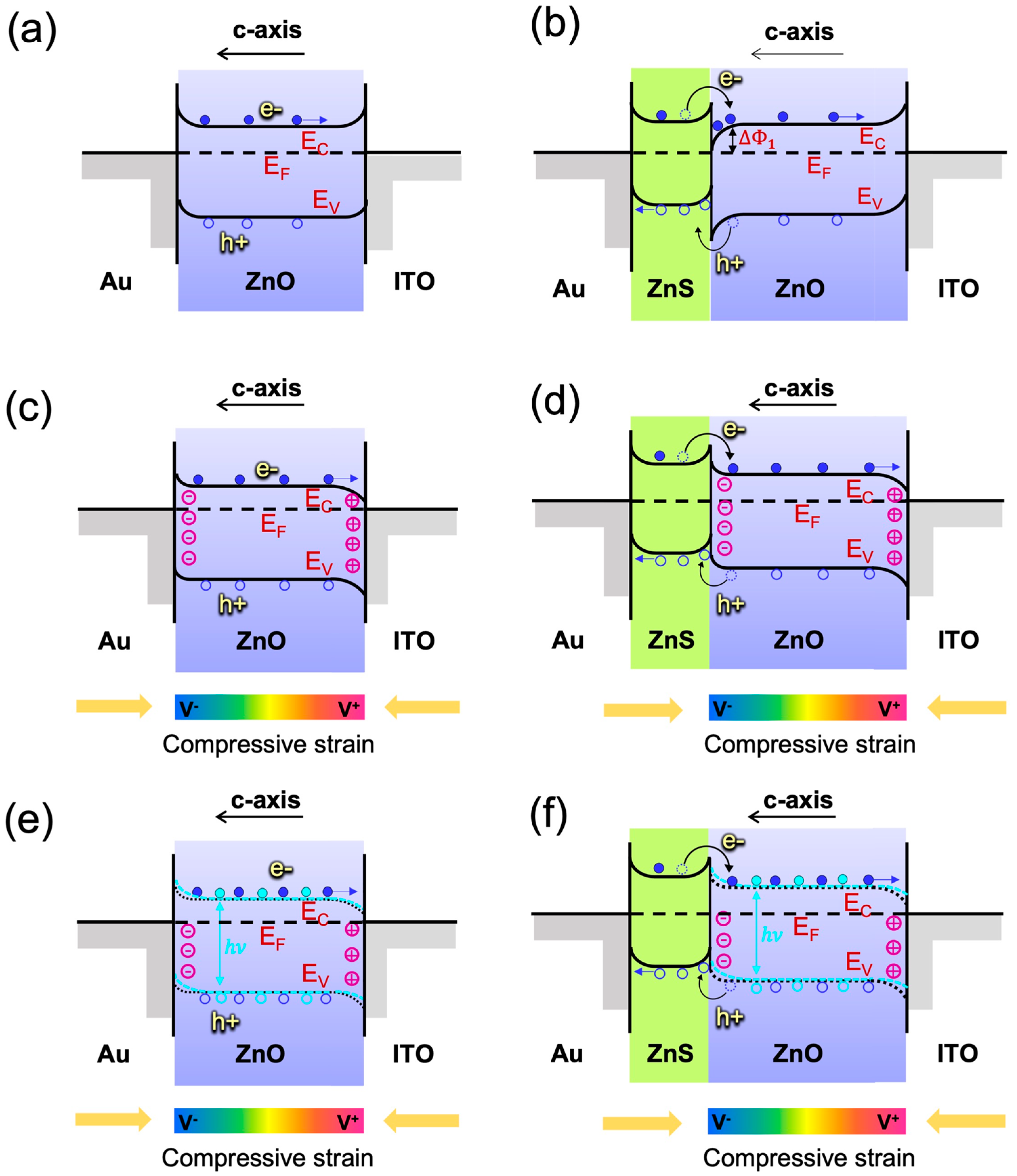
To elucidate the piezotronic and piezo-phototronic behavior of the ZnO and ZnO/ZnS core/shell NWs, energy-band diagrams with the corresponding realignment of the band position under compressive strain are illustrated in
Figure 6.
Figure 6a,b show the energy-band diagram of the unstrained ZnO and ZnO/ZnS core/shell NWs with back-to-back Schottky contact at the external bias. The Schottky junctions can be formed at the interface regions between metals and semiconductors, such as ZnO/ITO, ZnO/Au, and ZnS/Au, because the work functions of ITO
and Au
are larger than those of ZnO
and ZnS
[
36,
37].
In particular, the energy-band diagram of the ZnO/ZnS core/shell NWs with a type-II band structure exhibited potential energy gradients with a staggered alignment at the heterojunction interface between ZnO and ZnS (
Figure 6b). These potential energy gradients can induce the separate confinement of the electrons and holes in the conduction band of ZnO core and the valence band of ZnS, respectively. Thus, this ideal distribution of charge carriers, where the electrons were confined in the ZnO NWs and the holes were confined in the ZnS shell, contributed to the enhanced charge transport. In addition, upon exposure to UV light, the recombination probability of the ZnO/ZnS core/shell NWs reduced because of the spatial separation of the photogenerated electrons and holes due to the type-II band alignment. In contrast, the recombination probability of the photogenerated carriers of the ZnO NWs increased because of their large number of surface states, which resulted in a low photocurrent.
When the substrate was bent into a convex configuration, the compressive strain was introduced along the
c-axis direction of the ZnO NWs, and the corresponding piezopotential distribution was also induced.
Figure 6c,d show that the positive piezoelectric charges were generated at the bottom of the tip of the ZnO NWs, and they induced the downward bending of the conduction and valence bands of the ZnO near the ITO. This indicates that the positive piezopotential modified the local SBH at the ZnO/ITO interfaces of both the ZnO and ZnO/ZnS core/shell NWs, thus facilitating the electrical transport. These features indicate that the piezoelectric charges and potential generated along the ZnO NWs play a crucial role in determining the movements of the electrons, which affects the properties of the device. In particular, in the case of the ZnO/ZnS core/shell NWs, a negative piezopotential at the heterojunction interfaces between ZnO and ZnS can eliminate the electron trap state barrier
, which is unfavorable for charge transport (
Figure 6d). This indicates that the electrical transport properties of ZnO/ZnS core/shell NWs can be further improved by applying an external strain.
Figure 6e,f show the change in the energy-band diagrams after UV light irradiation under applied strain. Similarly, strain-induced positive piezoelectric charges under UV irradiation reduced the SBH at the interfacial region between the ZnO and ITO. Consequently, more photogenerated electrons can be transferred from ZnO to ITO electrodes, resulting in an increase in the photocurrent and responsivity. The charge carrier transport of the ZnO/ZnS core/shell NWs was significantly enhanced in the type-II alignment due to the combined effect of the piezopotential and photo-excitation, thereby resulting in a higher current and responsivity change when the NWs were simultaneously subjected to strain and illumination. However, it is important to note that the photogenerated electrons that reside in the conduction band of ZnO are attracted to a positive piezopotential, resulting in a partially weakened piezopotential [
34]. Thus, the dependence on strain becomes less sensitive under UV irradiation because the piezopotential is weakened by the screening effect induced by the photoexcited electrons and holes [
33]. If the illumination power density is sufficiently high, the piezopotential can be completely eliminated by the screening effect [
33]. Nonetheless, both strain and light act synergistically to increase the conductance, resulting in a higher current at the same bias and illumination than that in the “no strain” condition.


