Article

Skin-Compatible Amorphous Oxide Thin-Film-Transistors with a Stress-Released Elastic Architecture

1
School of Electrical and Electronics Engineering, Chung-Ang University, Seoul 06974, Korea
2
Department of Electrical Engineering, University of Cambridge, Cambridge CB2 1TN, UK
3
School of Advanced Materials Science and Engineering, Sungkyunkwan University, Suwon 16419, Korea
*
Authors to whom correspondence should be addressed.
Appl. Sci. 2021, 11(12), 5501; https://doi.org/10.3390/app11125501
Submission received: 30 May 2021 / Revised: 8 June 2021 / Accepted: 11 June 2021 / Published: 14 June 2021
(This article belongs to the Special Issue Applications of Nano-Electronic Devices)

Abstract

:
A highly reliable reverse-trapezoid-structured polydimethylsiloxane (PDMS) is demonstrated to achieve mechanically enhanced amorphous indium-gallium-zinc oxide (a-IGZO) thin-film-transistors (TFTs) for skin-compatible electronics. Finite element analysis (FEA) simulation reveals that the stress within a-IGZO TFTs can be efficiently reduced compared to conventional substrates. Based on the results, a conventional photolithography process was employed to implement the reverse-trapezoid homogeneous structures using a negative photoresist (NPR). Simply accessible photolithography using NPR enabled high-resolution patterning and thus large-area scalable device architectures could be obtained. The a-IGZO TFTs on the reverse-trapezoid-structured PDMS exhibited a maximum saturation mobility of 6.06 cm2V−1s−1 under a drain bias voltage of 10 V with minimal strain stress. As a result, the proposed a-IGZO TFTs, including stress-released architecture, exhibited highly enhanced mechanical properties, showing saturation mobility variation within 12% under a strain of 15%, whereas conventional planar a-IGZO TFTs on PDMS showed mobility variation over 10% even under a 1% strain and failed to operate beyond a 2% strain.

1. Introduction

Mechanically stretchable electronic devices are attracting great attention due to their conformable adaptability to the human body [1,2,3]. The advantage of being conformable devices leads to the creation of utilization of wearable s and healthcare monitoring systems, as well as human-machine interfaces, smart skin, and robotics applications [4,5,6,7,8]. In addition to the above promise, the capability of resisting various deformations may enable the realization of rollable and stretchable displays [9]. The meaningful realization of skin-compatible electronic devices requires achievement of physical parameters that approximate those of the human epidermis to be properly compliant and contact with the skin. To do this, the skin-compatible electronic applications should not only be bent to conform to the skin topography but also to be stretchable to accommodate strain from various body motions. Thus, skin-compatible devices can elastically deform with a minimum 15% strain of the epidermis [2]. To meet these needs, one of the most commonly used elastomeric materials is polydimethylsiloxane (PDMS), which has an elastic modulus similar to that of human skin, shows optimal conformability and good contact and adhesion to the skin [2,10].
The achievement of practical skin-compatible electronic applications requires progress in the robustness of stretchable thin film transistors (TFTs) as the indispensable basic components of various systems. Among a variety of semiconductor materials, amorphous indium-gallium-zinc oxide (a-IGZO) thin films have been extensively employed in switching components in large area displays, sensors and functional circuits because of their outstanding electrical performance and excellent features such as low off current, high mobility, good transparency, and easy fabrication from inexpensive precursors [1,11,12,13,14]. However, the oxide materials have inherent limitations in mechanical properties, such as high brittleness and fragileness [15]. Therefore, it has been a significant challenge to implement highly reliable and robust oxide thin films onto complaint and ultraflexible substrates, allowing tolerance of large strains without significant degradation of electrical properties and the fracture of a-IGZO TFTs and their integrated circuits.
To implement stretchable amorphous metal-oxide electronics with high mechanical stability, diverse unique structures have been suggested such as transferred device architectures on heterogeneous rigid island substrates, and strain-minimized device structures on dome-like deformable substrates [16,17]. For example, prestrained wavy geometry of ZnO TFTs [18] and integrated a-IGZO TFTs on a strain-relief rigid island to protect the electronic devices from severe cracking [19,20] have been demonstrated. Although previous advances are noteworthy, heterogeneous structures including stiff islands located under TFT devices often exhibit operational failures possibly due to the delamination between elastomeric parts and rigid islands in the substrates, which may be caused by enhanced strain from remaining portion of the stiff islands [17,21].
Despite these advances, more versatility and feasibility of stretchable electronic devices, it is highly desirable to achieve enhanced mechanical properties along with high density of device integration for simple process. Thus, to realize skin-compatible electronics, we propose reverse-trapezoid-structured a-IGZO TFTs in a stretchable matrix by employing a complementary metal–oxide semiconductor-compatible photolithography process with commercialized homogeneous elastomeric materials.

2. Materials and Methods

For the sacrificial layer, 15 wt% polyimide (PI) varnish (Polyzen 150, Picomax) was coated on a carrier glass at a spin speed of 4000 rpm for 60 s and was thermally cured at 300 °C for 1 h in air, resulting in a thickness of <3 μm.
For the solution-processed a-IGZO TFTs, a thermal evaporator system was utilized to deposit a 5 nm Cr and a 45 nm Au gate electrode at a 0.1 Åsec−1 deposition rate on the sacrificial PI substrate. By using photolithography with an AZ GXR-601 photoresist (Merck) and wet-etching process, the gate electrode and the following thin film layers were patterned. After patterning the gate electrode, an atomic-layer-deposition system (ALD) was used to deposit a 50 nm Al2O3 gate dielectric layer at 150 °C using trimethylaluminum as the Al precursor and deionized water as the oxygen source. Before patterning the gate dielectric layer, combustive a-IGZO solutions were coated at a spin speed of 2000 rpm for 20 s and a deep ultra-violet (DUV) process was carried out to obtain a 10 nm-thick a-IGZO active layer. The combustion a-IGZO solution was prepared by dissolving metal precursors in anhydrous 2-methoxyethnaol and sequentially adding acetylacetone and ammonium hydroxide. The metal precursors included indium nitrate hydrate (In(NO3)3·xH2O), gallium nitrate hydrate (Ga(NO3)3·xH2O) and zinc nitrate hydrate (Zn(NO3)3·xH2O) [11,14]. After the DUV annealing process, the a-IGZO active layer and Al2O3 gate dielectric layer were sequentially patterned. For the formation of source/drain electrodes, an RF sputtering system was used to deposit a 100 nm-thick IZO layer (power: 150 W, pressure: 1.5 mTorr, time: 3 min). The IZO source/drain electrodes were patterned by a lift-off process using a negative photoresist (NPR) (NR9-300PY, Futurrex, Franklin, NJ, USA).
For the formation of the reverse-trapezoid structure, the NPR was spin-coated at a spin speed of 500 rpm for 20 s onto the fully fabricated a-IGZO TFTs on a sacrificial PI substrate and patterned by a photolithography process to obtain undercut structures which act as pivotal molds to generate the reverse-trapezoid structure for skin-compatible and stretchable PDMS (Sylgard 184, Dow Corning, Midland, MI, USA). The thickness and undercut structures were controlled by the spin speed and development time, respectively. The PDMS solution was then coated at a spin speed of 200 rpm for 60 s and thermally cured at 80 °C for 12 h in air. The PDMS solution was mixed with 10:1 weight ratio of base agent to curing agent and was degassed in a vacuum chamber for 20 min to eliminate air bubbles. Finally, the fabricated devices were mechanically detached from the carrier glass, and the sacrificial PI layer was eliminated by O2 plasma treatment at 200 W for 13 min [22]. The remaining NPR layers and by-products were removed by dipping in acetone as shown in Figure S1.
For finite element analysis (FEA) simulation, a numerical model was validated by commercial COMSOL Multiphysics 5.3. Each thin film layer was modeled by the linear elastic material properties listed in Table 1. The simulated models of conventional and proposed structures resulted in calculation of 2-D planes for simplicity and the uniaxial stretching experiment.
All the electrical measurements in the experiments were carried out in air ambient darkness. A semiconductor parameter analyzer (4156C, Agilent) was used to characterize the electrical properties of a-IGZO TFTs.
For scanning electron microscopy (SEM), a cross-section view was analyzed by a JSM-7055F Prime (JEOL Ltd.) at an operation voltage of 15 kV. The elastomeric samples were polished by LaboPol-30 (Struers) before the SEM analysis.

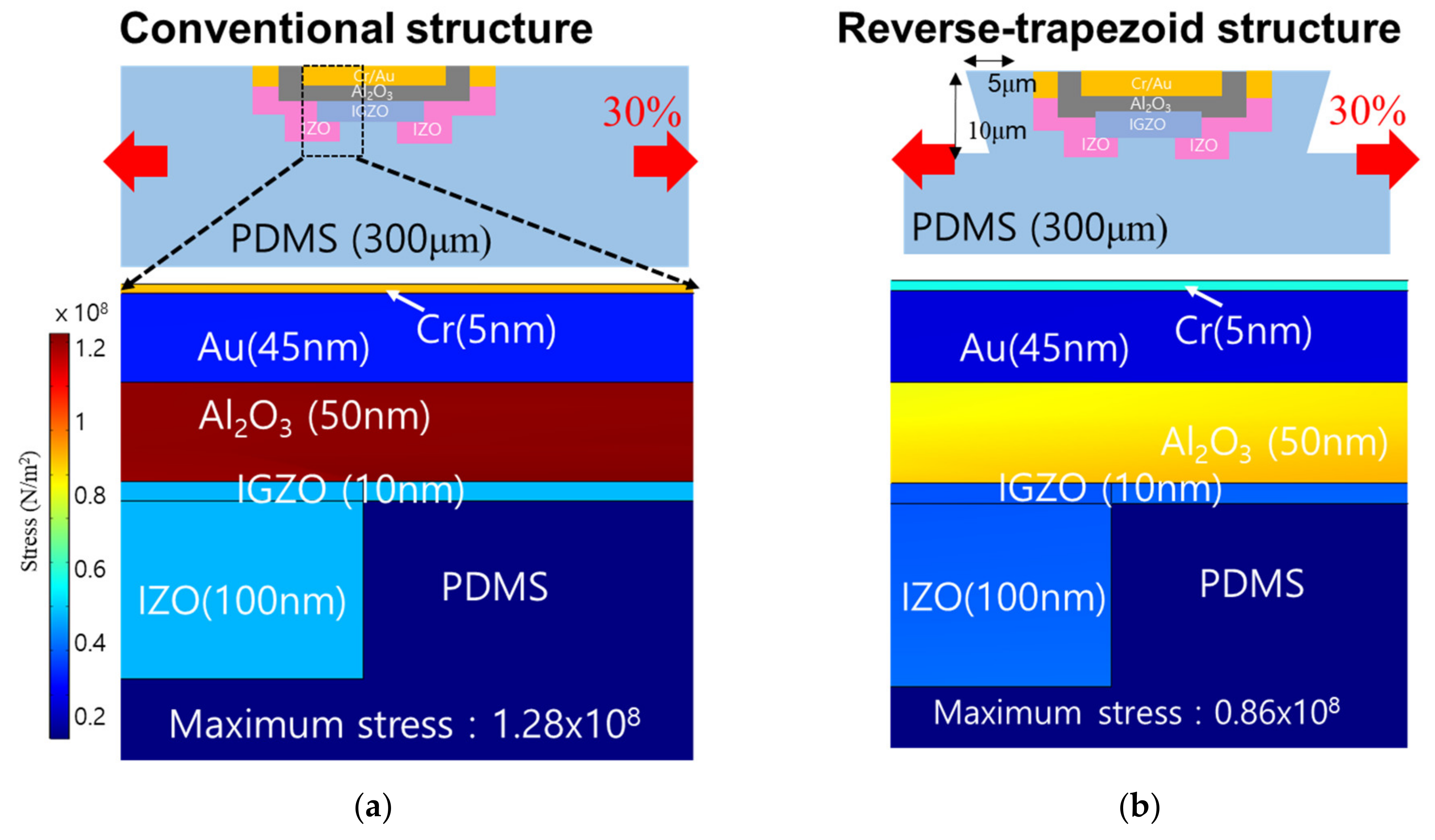
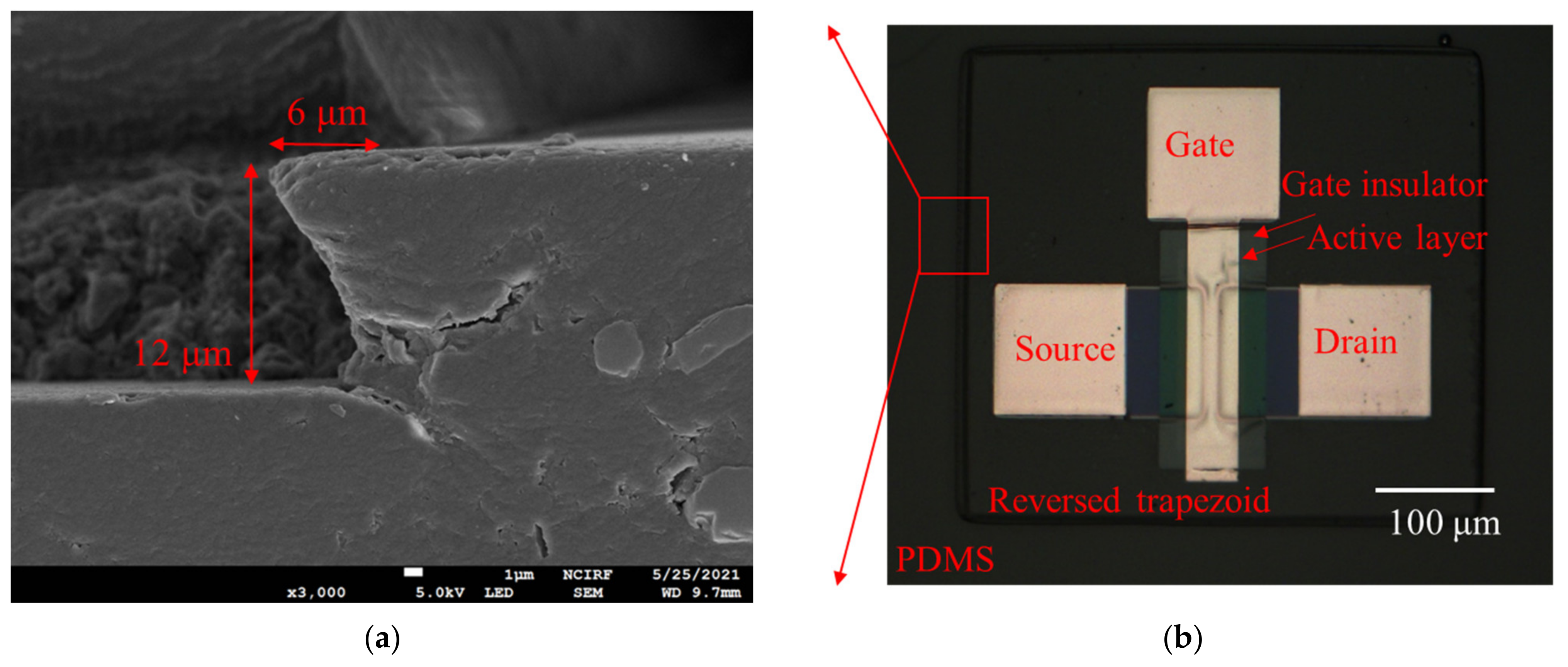
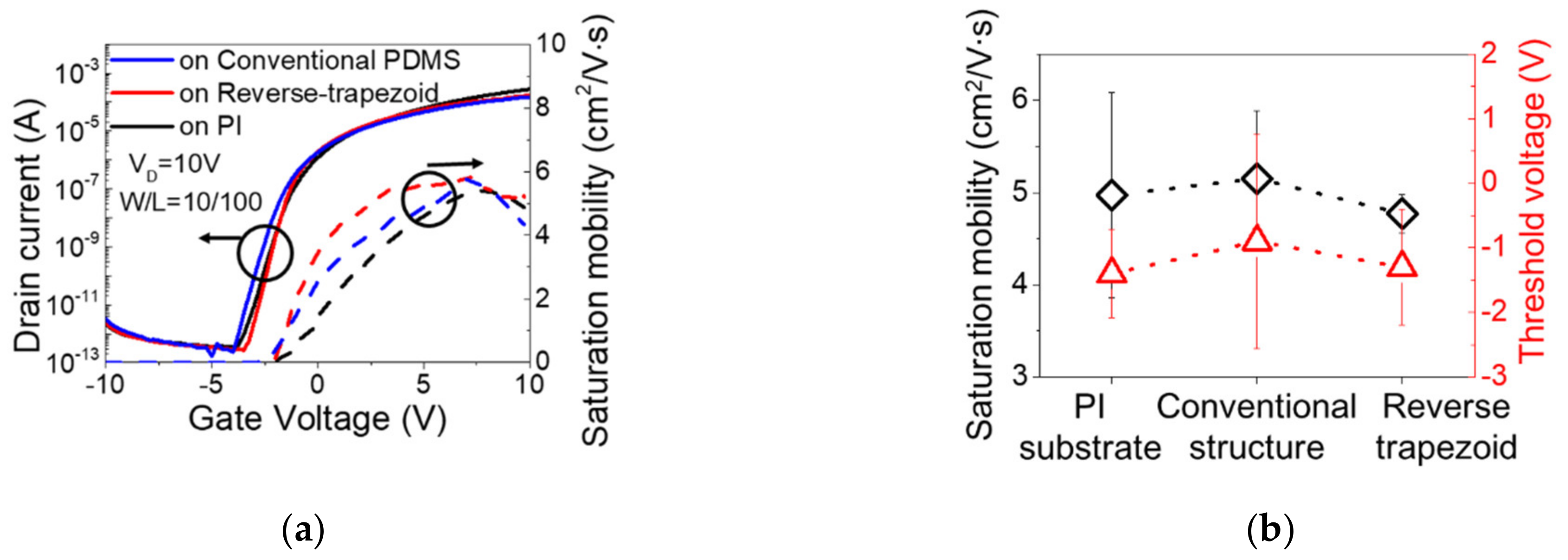
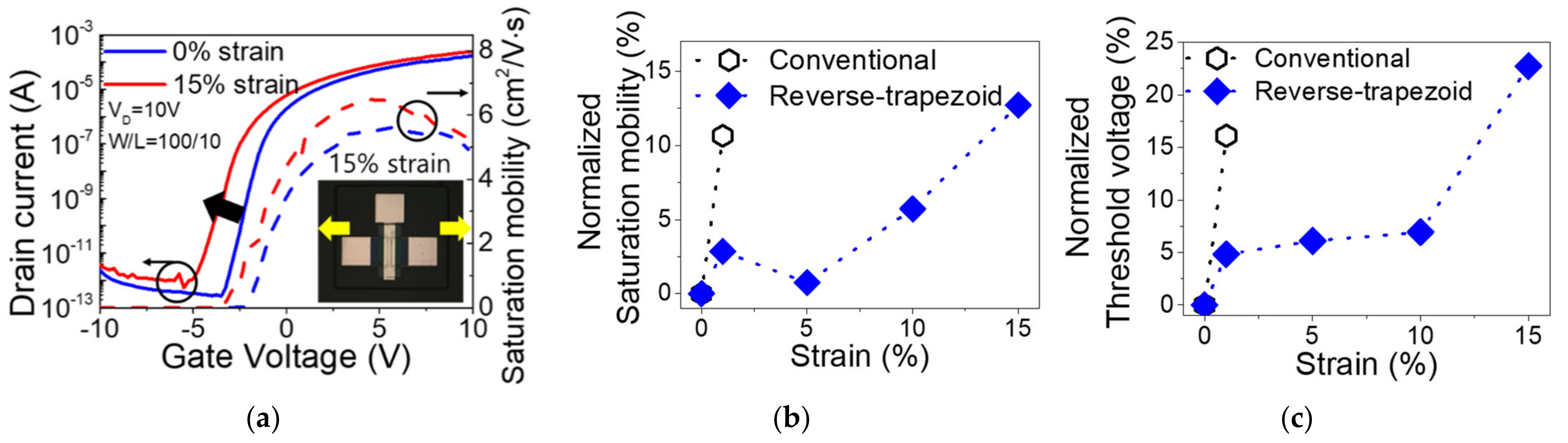
3. Results and Discussion

To investigate the effect of the proposed reverse-trapezoid architecture on mechanical stress distributions in stretchable a-IGZO TFTs, FEA simulations were performed on conventional and reverse-trapezoid-structured PDMS substrates by using COMSOL Multiphysics. The corresponding models for a-IGZO TFTs on elastomeric PDMS are shown in Figure 1. In this modelling, a 30% lateral strain was applied to the a-IGZO TFT by considering the maximum strain of the epidermis [23,24]. As shown in Figure 1, the highest stress was induced in the gate dielectric layer for the conventional PDMS substrate because of the large Young’s modulus of Al2O3 (Table 1) [25]. Importantly, this simulation suggests that the reverse-trapezoid structure can efficiently lower the stress distributions in the whole region of the stretchable a-IGZO TFTs compared to conventional PDMS, as shown in Figure 1a,b. In particular, the maximum stress induced in the a-IGZO TFT on a reverse-trapezoid PDMS substrate was 0.86 × 10⁸ Nm−2, which is lower than that on a conventional planar PDMS substrate (1.28 × 10⁸ Nm−2). For the reverse-trapezoid structure, the thickness and the undercut depth were varied to achieve the most effective architecture in FEA simulation. We assumed that the underlying mechanism of stress relaxation was the presence of the undercut, transforming the lateral force of strain to a vertical direction without a deteriorative effect on the a-IGZO TFTs. As a result, the reverse-trapezoid structure for stretchable a-IGZO TFTs had the effect of releasing the stress induced by the strain. Additionally, undercut depths over the specific value prevented most advantages of the reverse-trapezoid structure, as shown in Figure S2.
Based on the FEA simulation results, the reverse-trapezoid architecture was utilized to fabricate solution-processed a-IGZO TFTs by a simple route using a photolithography process. As shown in Figure 2a, the cross-sectional view of the SEM image confirms that pouring onto the mold generated a trapezoidal edge as a copy of the NPR undercut by fully filling the undercut space. Here, we used an epoxy material instead of PDMS to prepare the SEM sample because the PDMS was sheered and squashed during the polishing process, providing a distorted cross-sectional view. The thickness and undercut depth of the fabricated architecture were set to values almost identical to the simulation data, where the thickness was 12 μm and the undercut was 6 μm. The optical microscope image of the stretchable a-IGZO TFTs is shown in Figure 2b. In contrast with the device on a PI substrate, the a-IGZO TFTs on a stretchable PDMS had top-gate, bottom-contact, and self-passivated structures after the mechanical transference and O2 plasma processes.
The effect of mechanical transference and O2 plasma processes on the electrical characteristics of a-IGZO TFTs was investigated as shown in Figure 3a,b. Because the a-IGZO TFTs were mechanically detached from a carrier glass and exposed to O2 plasma to etch the sacrificial PI layer, there were concerns about the harmful effects on a-IGZO TFT devices by mechanical stress and plasma bombardment during the fabrication. The stretchable a-IGZO TFTs on a reverse-trapezoid PDMS had an average saturation mobility of 4.77 cm2 V−1s−1 and threshold voltage of −1.3 V. After fully transferring to the PDMS, the variation of saturation mobility was less than 4%, and negligible changes of threshold voltage were observed for both a-IGZO TFTs on conventional and reverse-trapezoid structures. Therefore, it can be suggested that the mechanical transference technique and the O2 plasma treatment barely affected the electrical performance, possibly assisted by the top-gate, bottom-contact, and self-passivated structure of the device.
As shown in Figure 4a, the a-IGZO TFTs showed proper switching behaviors with an on/off ratio of >108 under 15% strain. The stretchable a-IGZO TFTs on conventional PDMS showed a variation of >10% for both saturation mobility and threshold voltage even under 1% strain, as shown in Figure 4b,c and Figure S3. On the contrary, the a-IGZO TFTs on the reverse-trapezoid PDMS showed about 5% variation of saturation mobility and threshold voltage under 10% strain. These variations in the electrical properties might be related to the generation of oxygen vacancy in a-IGZO thin-films by the mechanical stress, leading to a negative threshold voltage shift and increased saturation mobility of a-IGZO TFTs [25,26,27]. Although the electrical changes abruptly increased over 10% under 15% strain, importantly, the stretchable a-IGZO TFTs on the reverse-trapezoid PDMS exhibited appropriate operation as switching devices to realize stretchable TFT-based skin-compatible applications.

4. Conclusions

In this study, with mechanical FEA simulation of stretchable device modelling, we were able to create a stress-released substrate for solution-processed a-IGZO TFTs by adopting a reverse-trapezoid structure. In particular, electrical analysis showed that the proposed process for the formation of the structure rarely affected the electrical properties of the device. Moreover, the electrical characteristics of stretchable a-IGZO TFTs were investigated under various strain elongations up to 15%, proving that the reverse-trapezoid structure successfully enhanced the mechanical robustness of a-IGZO TFTs for skin-compatible applications.

Supplementary Materials

The following are available online at https://www.mdpi.com/article/10.3390/app11125501/s1, Figure S1: The fabrication steps for reverse-trapezoid-structured a-IGZO TFTs, Figure S2: The maximum stress induced within a-IGZO TFT devices on reverse-trapezoid substrates with various undercut dimensions, Figure S3: Transfer characteristics and saturation mobility of a-IGZO TFTs on conventional PDMS.

Author Contributions

Conceptualization, K.-T.K., S.-H.K., S.-K.P.; methodology, K.-T.K., S.-J.N.; software, S.-H.K., C.-Y.P.; formal analysis, K.-T.K., J.-W.J.; writing—original draft preparation, K.-T.K.; writing—review and editing, K.-T.K., J.-S.H., S.-K.P.; supervision, J.-S.H., S.-K.P. All authors have read and agreed to the published version of the manuscript.

Funding

This research was partially funded by the Technology Innovation Program (20012617, Core technology development of CMOS device fabrication using nonsilicon semiconductor thin film trsnsistors for high resolution large area display) funded By the Ministry of Trade, Industry & Energy(MOTIE, Korea), by the Competency Development Program for Industry Specialists of the Korean Ministry of Trade, Industry and Energy (MOTIE), operated by Korea Institute for Advancement of Technology (KIAT). (No. P0002397, HRD program for Industrial Convergence of Wearable Smart Devices, and by the Chung-Ang University Graduate Research Scholarship in 2020.

Institutional Review Board Statement

Not applicable.

Informed Consent Statement

Not applicable.

Data Availability Statement

The data presented in this study are available on request from the corresponding author.

Conflicts of Interest

Authors declare no conflict of interest.

References

  1. Wang, B.; Thukral, A.; Xie, Z.; Liu, L.; Zhang, X.; Huang, W.; Yu, X.; Yu, C.; Marks, T.J.; Facchetti, A. Flexible and stretchable metal oxide nanofiber networks for multimodal and monolithically integrated wearable electronics. Nat. Commun. 2020, 11, 1–11. [Google Scholar]
  2. Liu, Y.; Pharr, M.; Salvatore, G.A. Lab-on-Skin: A Review of Flexible and Stretchable Electronics for Wearable Health Monitoring. ACS Nano 2017, 11, 9614–9635. [Google Scholar] [CrossRef] [PubMed]
  3. Park, S.; Heo, S.W.; Lee, W.; Inoue, D.; Jiang, Z.; Yu, K.; Jinno, H.; Hashizume, D.; Sekino, M.; Yokota, T.; et al. Self-powered ultra-flexible electronics via nano-grating-patterned organic photovoltaics. Nature 2018, 561, 516–521. [Google Scholar] [CrossRef] [PubMed]
  4. Wang, S.; Xu, J.; Wang, W.; Wang, G.J.N.; Rastak, R.; Molina-Lopez, F.; Chung, J.W.; Niu, S.; Feig, V.R.; Lopez, J.; et al. Skin electronics from scalable fabrication of an intrinsically stretchable transistor array. Nature 2018, 555, 83–88. [Google Scholar] [CrossRef]
  5. Hua, Q.; Sun, J.; Liu, H.; Bao, R.; Yu, R.; Zhai, J.; Pan, C.; Wang, Z.L. Skin-inspired highly stretchable and conformable matrix networks for multifunctional sensing. Nat. Commun. 2018, 9, 1–11. [Google Scholar] [CrossRef]
  6. Someya, T.; Amagai, M. Toward a new generation of smart skins. Nat. Biotechnol. 2019, 37, 382–388. [Google Scholar] [CrossRef] [PubMed]
  7. Kim, D.H.; Xiao, J.; Song, J.; Huang, Y.; Rogers, J.A. Stretchable, curvilinear electronics based on inorganic materials. Adv. Mater. 2010, 22, 2108–2124. [Google Scholar] [CrossRef]
  8. Kim, D.H.; Rogers, J.A. Stretchable electronics: Materials strategies and devices. Adv. Mater. 2008, 20, 4887–4892. [Google Scholar] [CrossRef]
  9. Koo, J.H.; Kim, D.C.; Shim, H.J.; Kim, T.H.; Kim, D.H. Flexible and Stretchable Smart Display: Materials, Fabrication, Device Design, and System Integration. Adv. Funct. Mater. 2018, 28, 1–23. [Google Scholar] [CrossRef]
  10. Cong, H.; Pan, T. Photopatternable conductive PDMS materials for microfabrication. Adv. Funct. Mater. 2008, 18, 1912–1921. [Google Scholar] [CrossRef]
  11. Kim, Y.-H.; Heo, J.-S.; Kim, T.-H.; Park, S.; Yoon, M.-H.; Kim, J.; Oh, M.S.; Yi, G.-R.; Noh, Y.-Y.; Park, S.K. Flexible metal-oxide devices made by room-temperature photochemical activation of sol-gel films. Nature 2012, 489, 128–132. [Google Scholar] [CrossRef]
  12. Kim, M.-G.; Kanatzidis, M.G.; Facchetti, A.; Marks, T.J. Low-temperature fabrication of high-performance metal oxide thin-film electronics via combustion processing. Nat. Mater. 2011, 10, 382–388. [Google Scholar] [CrossRef]
  13. Kang, T.S.; Kim, T.Y.; Lee, G.M.; Sohn, H.C.; Hong, J.P. Highly stable solution-processed ZnO thin film transistors prepared via a simple Al evaporation process. J. Mater. Chem. C 2014, 2, 1390. [Google Scholar] [CrossRef]
  14. Kim, K.T.; Jeon, S.P.; Lee, W.; Jo, J.W.; Heo, J.S.; Kim, I.; Kim, Y.H.; Park, S.K. A Site-Specific Charge Carrier Control in Monolithic Integrated Amorphous Oxide Semiconductors and Circuits with Locally Induced Optical-Doping Process. Adv. Funct. Mater. 2019, 29, 1–9. [Google Scholar] [CrossRef]
  15. Chen, Z.; Cotterell, B.; Wang, W. The fracture of brittle thin films on compliant substrates in flexible displays. Eng. Fract. Mech. 2002, 69, 597–603. [Google Scholar] [CrossRef]
  16. Münzenrieder, N.; Cantarella, G.; Vogt, C.; Petti, L.; Büthe, L.; Salvatore, G.A.; Fang, Y.; Andri, R.; Lam, Y.; Libanori, R.; et al. Stretchable and Conformable Oxide Thin-Film Electronics. Adv. Electron. Mater. 2015, 1, 1–7. [Google Scholar] [CrossRef]
  17. Matsuhisa, N.; Kaltenbrunner, M.; Yokota, T.; Jinno, H.; Kuribara, K.; Sekitani, T.; Someya, T. Printable elastic conductors with a high conductivity for electronic textile applications. Nat. Commun. 2015, 6. [Google Scholar] [CrossRef] [PubMed]
  18. Park, K.; Lee, D.K.; Kim, B.S.; Jeon, H.; Lee, N.E.; Whang, D.; Lee, H.J.; Kim, Y.J.; Ahn, J.H. Stretchable, transparent zinc oxide thin film transistors. Adv. Funct. Mater. 2010, 20, 3577–3582. [Google Scholar] [CrossRef]
  19. Romeo, A.; Lacour, S.P. Stretchable metal oxide thin film transistors on engineered substrate for electronic skin applications. In Proceedings of the 2015 37th Annual International Conference of the IEEE Engineering in Medicine and Biology Society (EMBC), Milan, Italy, 25–29 August 2015; pp. 8014–8017. [Google Scholar]
  20. Park, C.W.; Moon, Y.G.; Seong, H.; Jung, S.W.; Oh, J.Y.; Na, B.S.; Park, N.M.; Lee, S.S.; Im, S.G.; Koo, J.B. Photolithography-Based Patterning of Liquid Metal Interconnects for Monolithically Integrated Stretchable Circuits. ACS Appl. Mater. Interfaces 2016, 8, 15459–15465. [Google Scholar] [CrossRef]
  21. Libanori, R.; Erb, R.M.; Reiser, A.; Le Ferrand, H.; Süess, M.J.; Spolenak, R.; Studart, A.R. Stretchable heterogeneous composites with extreme mechanical gradients. Nat. Commun. 2012, 3, 1–9. [Google Scholar] [CrossRef] [Green Version]
  22. Kim, K.T.; Kang, S.H.; Kim, J.; Heo, J.S.; Kim, Y.H.; Park, S.K. An Ultra-Flexible Solution-Processed Metal-Oxide/Carbon Nanotube Complementary Circuit Amplifier with Highly Reliable Electrical and Mechanical Stability. Adv. Electron. Mater. 2019, 1900845, 1–8. [Google Scholar] [CrossRef]
  23. Hanif, A.; Bag, A.; Zabeeb, A.; Moon, D.B.; Kumar, S.; Shrivastava, S.; Lee, N.E. A Skin-Inspired Substrate with Spaghetti-Like Multi-Nanofiber Network of Stiff and Elastic Components for Stretchable Electronics. Adv. Funct. Mater. 2020, 30, 1–10. [Google Scholar] [CrossRef]
  24. Kim, D.-H.; Lu, N.; Ma, R.; Kim, Y.-S.; Kim, R.-H.; Wang, S.; Wu, J.; Won, S.M.; Tao, H.; Islam, A.; et al. Epidermal Electronics. Science 2011, 333, 838–844. [Google Scholar] [CrossRef] [PubMed] [Green Version]
  25. Kim, K.; Moon, S.; Kim, M.; Jo, J.; Park, C.; Kang, S.; Kim, Y.; Park, S.K. Highly Scalable and Robust Mesa-Island-Structure Metal-Oxide Thin-Film Transistors and Integrated Circuits Enabled by Stress-Diffusive Manipulation. Adv. Mater. 2020, 32, 2003276. [Google Scholar] [CrossRef] [PubMed]
  26. Billah, M.M.; Hasan, M.M.; Jang, J. Effect of tensile and compressive bending stress on electrical performance of flexible a-IGZO TFTs. IEEE Electron. Device Lett. 2017, 38, 890–893. [Google Scholar] [CrossRef]
  27. Lee, S.; Jeong, D.; Mativenga, M.; Jang, J. Highly Robust Bendable Oxide Thin-Film Transistors on Polyimide Substrates via Mesh and Strip Patterning of Device Layers. Adv. Funct. Mater. 2017, 27, 1–9. [Google Scholar] [CrossRef]
Figure 1. FEA modelling for stretchable a-IGZO TFTs. Stress distributions of a-IGZO TFTs under 30% strain on a PDMS substrate having (a) conventional structure and (b) reverse-trapezoid structure.
Applsci 11 05501 g001
Figure 2. Micrograph images of fabricated stretchable a-IGZO TFTs. (a) An SEM image for edge of reverse-trapezoid structure. (b) An image of fully fabricated stretchable a-IGZO TFTs on the reverse-trapezoid structure.
Applsci 11 05501 g002
Figure 3. Effects of substrate types on the electrical properties of a-IGZO TFTs. (a) Transfer characteristics, (b) the saturation mobility and threshold voltage of a-IGZO TFTs on various substrates.
Applsci 11 05501 g003
Figure 4. Electrical characteristics of stretchable a-IGZO TFTs on conventional and reverse-trapezoid PDMS. (a) Transfer characteristics of stretchable a-IGZO TFTs under a 15% strain. Variation of normalized (b) saturation mobility and (c) threshold voltage of stretchable a-IGZO TFTs on a conventional and a reverse-trapezoid PDMS as a function of strain.
Applsci 11 05501 g004
Table 1. Material properties of stretchable a-IGZO TFTs for the FEA simulation.
MaterialsCrAuAl2O3IGZOIZOPDMS
Density [kg/m3]715019,300396556007120970
Young’s modulus [GPa]27970400137137750 × 106
Poisson’s ratio0.210.440.220.360.360.49
Publisher’s Note: MDPI stays neutral with regard to jurisdictional claims in published maps and institutional affiliations.

