3. Results of the Characterizations of the Recast Layer
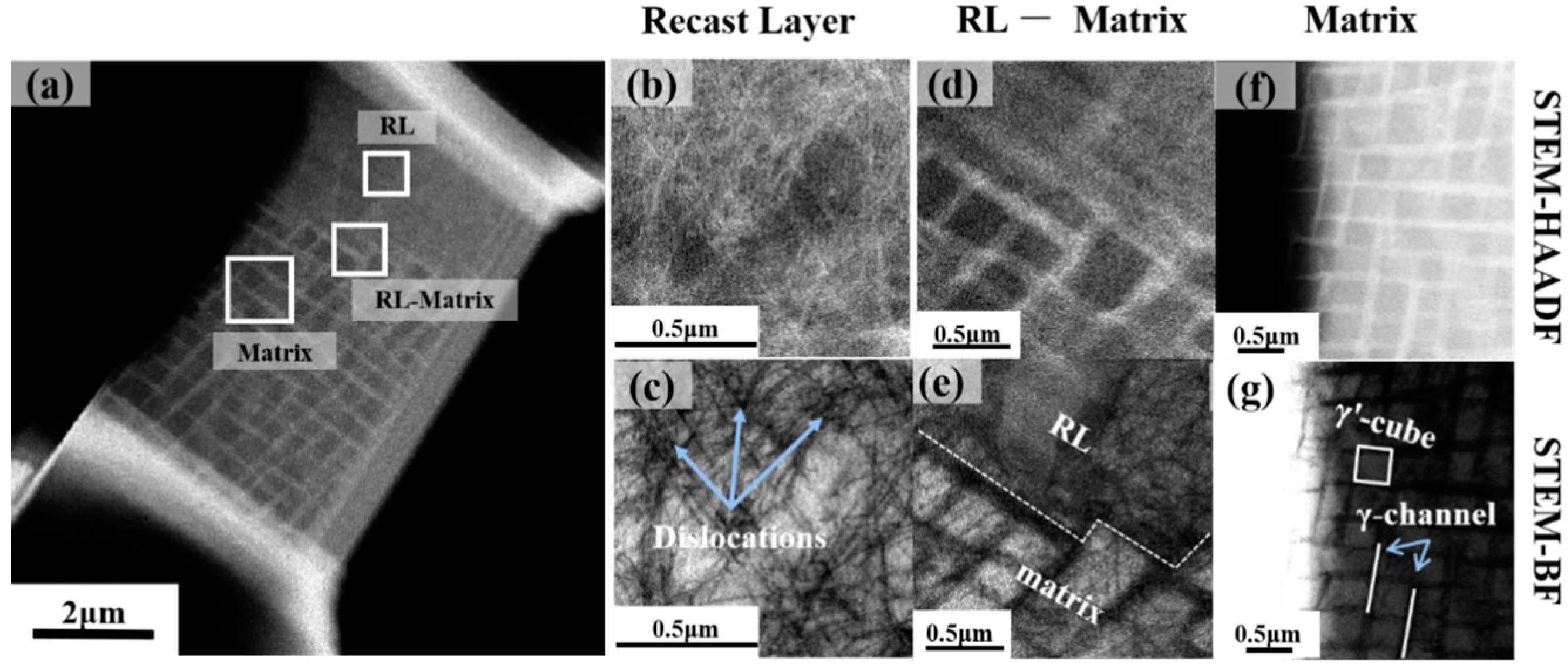
Figure 2 shows a scanning transmission electron microscopy high angle annular dark field (STEM-HAADF) image of the sample. There are three different regions, which are marked as RL, RL–matrix, and matrix in
Figure 2a, which were selected for further TEM analyses. It is obvious that the recast layer and the matrix show a significantly different microstructure. In the matrix, the typical γ’-cube precipitation is regularly distributed in the γ phase, while in the recast layer, the uniform image indicates a single-phase structure without any precipitation. As illustrated in
Figure 2b,c, both the dark field (DF) and bright field (BF) images show a large number of dislocations distributing in the recast layer, while the matrix consists of the γ channel and cubical γ’ phase (
Figure 2f,g). A clear boundary can be detected between the RL and the matrix, as shown in
Figure 2d,e.
To further identify the phase compositions of the two regions, the selected area electron diffraction (SAED) patterns of the recast layer and the matrix are presented in
Figure 3. The diffraction patterns in the recast layer and the matrix were obtained under the same tilting condition. The BF image and corresponding SAED pattern in
Figure 3a,b indicate that the RL consists of only a single FCC phase. Meanwhile, the SAED pattern in the matrix in
Figure 3c,d shows the superlattice of the L1
2 phase, corresponding to the γ’ precipitation. Combined with
Figure 2, it reveals that after high-temperature melting and rapid quenching, the epitaxial growth of molten metal occurs from the single-crystal matrix, and the same crystal orientation is maintained as the same as the matrix. The excessive cooling rate prevents the precipitation of the γ’ phase during the rapid solidification process. The recast layer continuously formed along the matrix with epitaxial growth is related to the continuous molten pool and temperature gradient generated during EDM. Each molten pool formed in the drilling process can be considered distributed perpendicular to the inner surface of the hole. This means that the molten pool is distributed in the same plane around the hole along the axial direction on the cross-section of the recast layer. The directional temperature gradient of the molten pool ensures the single-crystal properties of the matrix and the recast layer after processing.
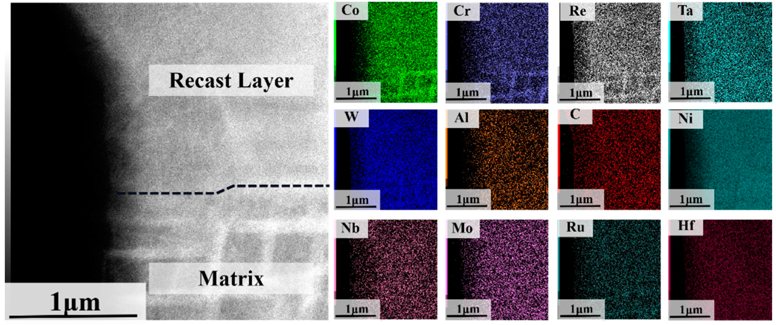
The composition of the recast layer and matrix were also identified with EDS in TEM. As shown in
Figure 4, Cr, Co and Re are concentrated in the γ phase of the selected matrix region, while this phenomenon does not exist in the recast layer region. The other elements do not vary significantly between the two regions. It is also shown that there is no compositional segregation in the recast layer, which further proves that no new phase is generated during the formation of the recast layer, which is consistent with the STEM and SAED analysis. The homogeneous redistribution of the elements in the recast layer is related to the rapid solidification experienced by the alloy in the process of electrical discharge. The alloy melts after reaching the melting point, and the elements are redistributed uniformly in the liquid. Then, the fast cooling leads to the absence of segregation, and there is no solute diffusion in the liquid. Accordingly, the recast layer only forms a single γ phase.
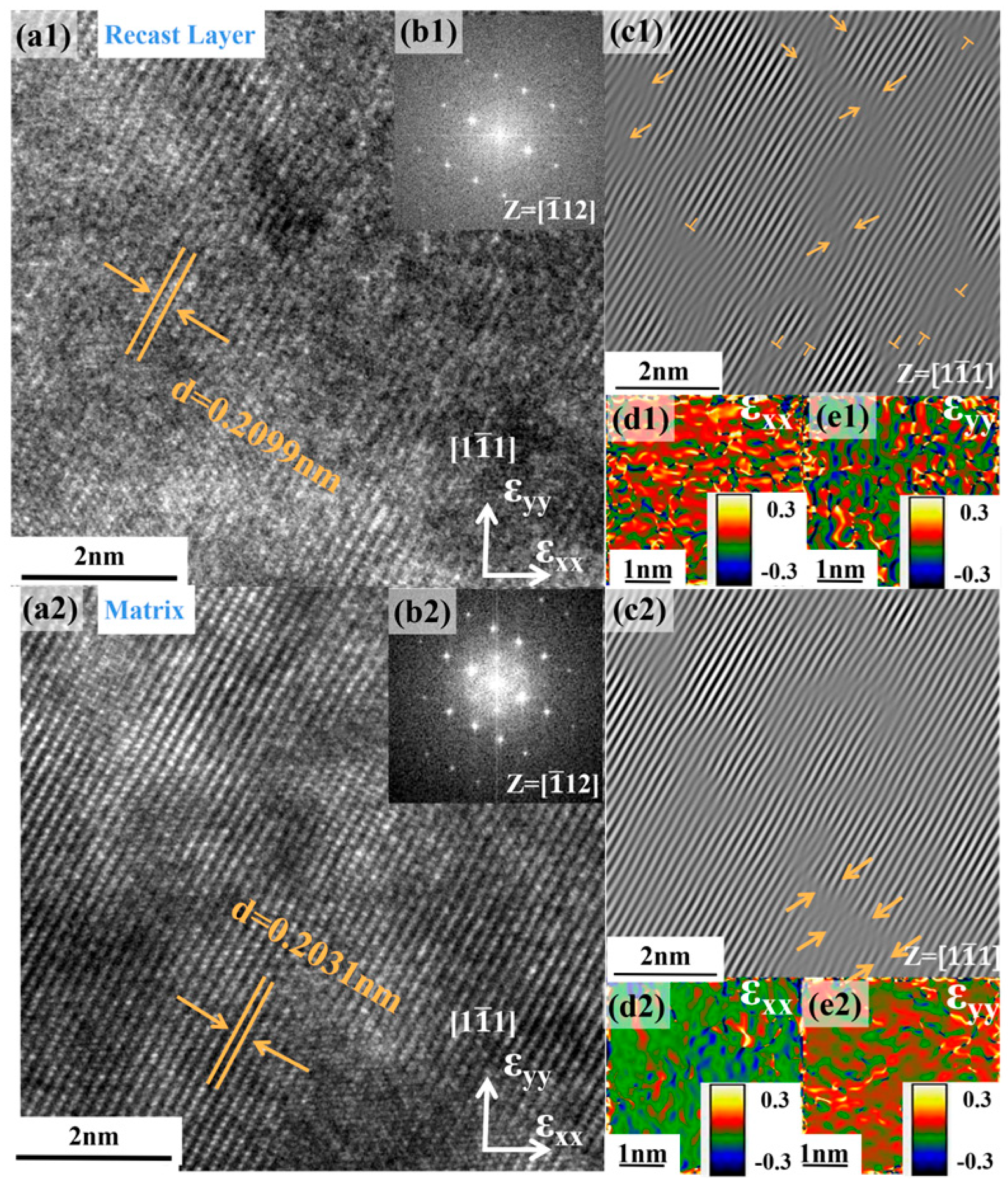
Figure 5 shows the high-resolution TEM (HR-TEM) images and geometric phase analysis of the recast layer and the matrix. The lattice spacing of (
) plane is estimated as 0.2099 nm in the recast layer, which is slightly larger than the lattice spacing of the FCC matrix (
Figure 5(a1,a2)). The larger lattice constant of the recast layer is due to the supersaturation of elements with larger atomic sizes. The alloying elements with large atomic radii are dissolved in the recast layer, resulting in a larger lattice constant than that of the matrix. This is consistent with the results shown in
Figure 4.
Using geometric phase analysis (GPA), it is found that there is a wide range of strain concentration areas in the given x and y directions of the recast layer (
Figure 5(d1,e1)), which is due to the high density of dislocations in the recast layer (
Figure 5(c1)). Moreover, the microscopic strain of the matrix itself is less obvious (
Figure 5(d2,e2)). The differences in lattice constants and microscopic strains between the recast layer and the matrix are closely related to the large number of dislocation defects caused by residual stress during machining, i.e., during the formation of the recast layer, it will be affected by multiple pulse discharges. With the increase in discharge times, the internal residual stress will gradually increase. In the process of forming the recast layer, there will be more dislocation density, resulting in more obvious distortion in the crystal lattice. This is one of the important reasons why there are more strain concentration areas in the recast layer in nanoscale GPA analyses.
According to the analyses shown in
Figure 2b,e, under the STEM of the FIB sample, there is a clear boundary between the recast layer and the matrix transition interface, which indicates that the transition area is very small. In order to determine the range of the heat-affected zone more accurately, the diffraction pattern difference and lattice constant change in the recast layer and the matrix on both sides of the interface are explored using a high-resolution transmission image.
Figure 6a shows the high-resolution transmission image (view field of 35 nm× 35 nm) near the transition region in the FIB sample.
Figure 6b,d shows the corresponding recast layer and matrix regions.
Figure 6c,e shows the corresponding diffraction patterns in different regions. It reveals that the distance between the [
] atomic plane in the recast layer is larger than that in the matrix. The position of the transition interface can be determined in this way. At the same time, the microstrain inside the heat-affected zone is analyzed. The geometric phase analysis of the microscopic strain distribution in the transition region is further shown in
Figure 6f,g. There are differences in the microscopic strain distribution in the transition interface in the x and y directions. The strain in the x direction near the matrix is mainly compressive strain, and the strain in the x direction near the recast layer is mainly tensile strain. This is mainly caused by the difference in the lattice constant of the recast layer and the matrix. The strain on both sides of the
y-axis direction is tensile strain. The crystal structure in both the recast layer and the matrix is FCC, but the lattice constant of the recast layer is larger than that of the matrix due to the single-phase structure and uniform distribution of elements. The strain in the x-direction difference in the transition region indicates the difference in the atomic arrangement between the recast layer and the matrix and explains the existence of a certain degree of misorientation between the recast layer and the matrix.
4. Discussion
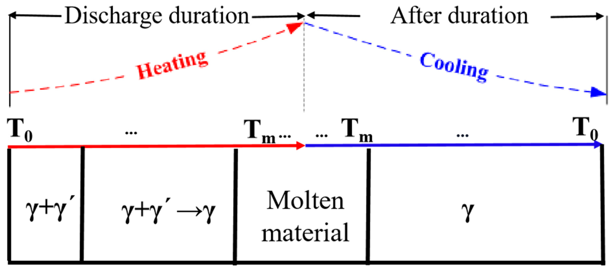
As the main result of the rapid melting and solidification process, the recast layer has many unique characteristics in terms of the forming method and structure compared with other materials. When the high-power energy of the single-crystal superalloy is given instantaneously, a directional temperature gradient will appear in the molten pool. The recast layer will achieve epitaxial growth along the direction of the single-crystal matrix during the high-temperature melting and rapid solidification process, maintain a continuous crystal orientation and finally grow into a single-crystal structure connected to the matrix material. For the discharge generated with multiple pulse cycles, the overlap and intersection of the molten pool further led to the emergence of the low-angle boundary. The nickel-based, single-crystal superalloy is mainly composed of the γ phase and γ’ phase.
The formation of the recast layer is a result of rapid melt–solidification, a typical process with many special features.
Figure 7 schematically shows the formation processes of the recast layer on the single-crystal superalloy. The pulse duration of EDM is very short. However, the highest temperature in the discharge process can increase rapidly over the melting point of the alloy. The γ phase and ordered L1
2 phase melt to form a liquid film. After the end of discharge, the cooling rate is more than 10
6 K/s, and the molten metal solidifies rapidly. The accelerated cooling rate prevents precipitation. In this process, the higher directional temperature gradient field makes the recast layer epitaxially grow along the matrix. At the same time, severe thermal stress generates, resulting in a much higher dislocation density in the recast layer region than that in the matrix region.
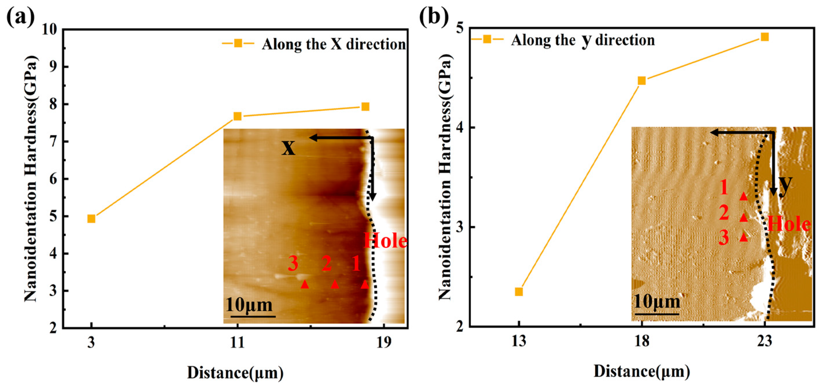
The recast layer around the cooling hole no longer contains the precipitated strengthening phase γ’, so the hardness may be lower than the matrix with precipitation.
Figure 8 shows the nanoindentation hardness of the film cooling hole wall at different locations along the hole wall–matrix direction (x direction) and the hole inlet–hole outlet direction (y direction). In
Figure 8a, the position far away from the hole wall is larger than 7 GPa. The three testing points in
Figure 8b are all located on the recast layer, and the hardness for all is smaller than 5 GPa. Compared with the hardness, point 1 in
Figure 8a at 3 μm near the hole wall may be adjacent to the recast layer. The nanohardness of point 2 and point 3 in
Figure 8a is not much different, and both are greater than point 1. Moreover, point 2 and point 3 are 11 μm and 19 μm away from the hole wall, respectively, and could be confirmed on the matrix due to the small range of the heat-affected zone [
19]. Based on
Figure 8a,b, it can be considered that the recast layer of the hole wall is much softer than the nearby alloy matrix. In addition, the nanohardness is lower than 5 GPa, while the hardness of the matrix in
Figure 8a is greater than 7 GPa. The hardness of the recast layer is lower than that of the matrix, which agrees with the microstructure analysis above. The molten metal is remelted and solidified to adhere to the hole wall, and the recast layer is determined to be a single-phase γ structure using various analysis methods and does not contain precipitated strengthening γ’ phase, so the overall hardness value is low.
Considering the varied nanohardness of the recast layer at different positions, the different mechanical behavior between the recast layer and the matrix may be a weakness at the crack initiation point. In the future, it is necessary to further confirm the hardness evolution of the recast layer during service. Moreover, the different oxidation behavior may be exhibited for different thicknesses of the recast layer.
Author Contributions
Conceptualization, Z.Y.; data Curation, L.L. and J.W.; formal analysis, Z.Y. and L.L.; resources, Z.Y.; writing—original draft preparation, Z.Y. and L.L.; supervision, J.W. and J.X.; validation, W.Z. and L.Z.; writing—review and editing, F.H. and Z.W.; project administration, Z.W. All authors have read and agreed to the published version of the manuscript.
Funding
The authors are grateful for support from the Research Fund of the State Key Laboratory of Solidification Processing (NPU), China (Grant No. 2022-BJ-03).
Data Availability Statement
The data presented in this study are available on request from the corresponding author.
Conflicts of Interest
The authors declare that they have no conflict of interest.
References
- Miller, R.A. Thermal barrier coatings for aircraft engines: History and directions. J. Therm. Spray Technol. 1997, 6, 35–42. [Google Scholar] [CrossRef] [Green Version]
- He, K. Investigations of film cooling and heat transfer on a turbine blade squealer tip. Appl. Therm. Eng. 2017, 110, 630–647. [Google Scholar]
- Liu, Y.; Ru, Y.; Zhang, H.; Pei, Y.; Li, S.; Gong, S. Coating-assisted deterioration mechanism of creep resistance at a nickel-based single-crystal superalloy. Surf. Coat. Technol. 2021, 406, 126668. [Google Scholar] [CrossRef]
- Wieghardt, K. Hot-Air Discharge for De-Icing; Wright Field, Air Materiel Command: Dayton, OH, USA, 1946; pp. 1–44. [Google Scholar]
- Bunker, R.S. A Review of Shaped Hole Turbine Film-Cooling Technology. J. Heat Transf. Trans. Asme 2005, 127, 441–453. [Google Scholar] [CrossRef]
- Ay, M.; Çaydaş, U.; Hasçalık, A. Optimization of micro-EDM drilling of inconel 718 superalloy. Int. J. Adv. Manuf. Technol. 2013, 66, 1015–1023. [Google Scholar] [CrossRef]
- Tao, X.; Liu, Z.; Qiu, M.; Tian, Z.; Shen, L. Research on an EDM-based unitized drilling process of TC4 alloy. Int. J. Adv. Manuf. Technol. 2018, 97, 867–875. [Google Scholar] [CrossRef]
- Li, C.; Xu, X.; Li, Y.; Tong, H.; Ding, S.; Kong, Q.; Zhao, L.; Ding, J. Effects of dielectric fluids on surface integrity for the recast layer in high speed EDM drilling of nickel alloy. J. Alloys Compd. 2019, 783, 95–102. [Google Scholar] [CrossRef]
- Pei, H.Q.; Wang, J.J.; Li, Z.; Li, Z.W.; Yao, X.Y.; Wen, Z.X.; Yue, Z.F. Oxidation behavior of recast layer of air-film hole machined by EDM technology of Ni-based single crystal blade and its effect on creep strength. Surf. Coat. Technol. 2021, 419, 127285. [Google Scholar] [CrossRef]
- Kuppan, P.; Rajadurai, A.; Narayanan, S. Influence of EDM process parameters in deep hole drilling of Inconel 718. Int. J. Adv. Manuf. Technol. 2008, 38, 74–84. [Google Scholar] [CrossRef]
- Wang, F.; Liu, Y.; Shen, Y.; Ji, R.; Tang, Z.; Zhang, Y. Machining Performance of Inconel 718 Using High Current Density Electrical Discharge Milling. Mater. Manuf. Process. 2013, 28, 1147–1152. [Google Scholar] [CrossRef]
- Tang, J.; Yang, X.A. novel thermo-hydraulic coupling model to investigate the crater formation in electrical discharge machining. J. Phys. D Appl. Phys. 2017, 50, 365301. [Google Scholar] [CrossRef]
- Tang, J.; Yang, X. Simulation investigation of thermal phase transformation and residual stress in single pulse EDM of Ti-6Al-4V. J. Phys. D Appl. Phys. A Europhys. J. 2018, 51, 135308. [Google Scholar] [CrossRef]
- Cusanelli, G.; Hessler-Wyser, A.; Bobard, F.; Demellayer, R.; Perez, R.; Flükiger, R. Microstructure at submicron scale of the white layer produced by EDM technique. J. Mater. Process. Technol. 2004, 149, 289–295. [Google Scholar] [CrossRef]
- Murray, J.W.; Fay, M.W.; Kunieda, M.; Clare, A.T. TEM study on the electrical discharge machined surface of single-crystal silicon. J. Mater. Process. Technol. 2013, 213, 801–809. [Google Scholar] [CrossRef]
- Liu, J.F.; Guo, Y.B.; Butler, T.M.; Weaver, M.L. Crystallography, compositions, and properties of white layer by wire electrical discharge machining of nitinol shape memory alloy. Mater. Des. 2016, 109, 1–9. [Google Scholar] [CrossRef] [Green Version]
- Li, C.; Zhang, B.; Li, Y.; Tong, H.; Ding, S.; Wang, Z.; Zhao, L. EDM/ECM high speed drilling of film cooling holes. J. Mater. Process. Technol. 2018, 262, 95–103. [Google Scholar] [CrossRef]
- Dong, T.; Gao, C.; Li, L.; Pei, Y.; Li, S.; Gong, S. Effect of substrate orientations on microstructure evolution and stability for single crystal superalloys in rapid solidification process. Mater. Des. 2017, 128, 218–230. [Google Scholar] [CrossRef]
- Shang, Y.; Zhang, H.; Hou, H.; Ru, Y.; Pei, Y.; Li, S.; Xu, H. High temperature tensile behavior of a thin-walled Ni based single-crystal superalloy with cooling hole: In situ experiment and finite element calculation. J. Alloys Compd. 2019, 782, 619–631. [Google Scholar] [CrossRef]
- Shi, Z.X.; Liu, S.Z.; Yue, X.D.; Wang, Z.C. Effect of Long Term Aging at 980 °C on Microstructure Stability of DD15 Single Crystal Superalloy. Fail. Anal. Prev. 2020, 15, 217–220. [Google Scholar]
Figure 1.
TEM sample preparation: (a) The selected specified region with both the matrix and recast layer. (b) Microstructure of the selected region. (c) The exact location of the TEM sample. (d) The prepared sample using FIB. The recast layer (left) and matrix (right) are shown in the sample.
Figure 2.
The detailed TEM analysis for the prepared sample: (a) The STEM-HAADF image of the overall microstructure. STEM-HAADF and STEM-BF images of (b,c) the recast layer, (d,e) the recast layer (RL) and matrix transition area and (f,g) the matrix of the sample. High-density dislocations are distributed over the area of the recast layer, while the matrix shows a typical γ’-γ microstructure.
Figure 3.
Selected area electron diffraction patterns of (a,b) the recast layer and (c,d) the matrix. The recast layer has a single-crystal structure with the same orientation in matrix.
Figure 4.
Energy dispersive spectroscopy area scanning profiles of the recast layer and matrix transition region. The composition of the recast layer area is uniform, and there is no segregation for all the elements.
Figure 5.
High-resolution transmission electron microscopy analyses of the recast layer (a1–e1) and the matrix (a2–e2). (a1,a2) HR-TEM atomic interface topographies. (b1,b2) Fast Fourier transform images. (c1,c2) Inverse fast Fourier transform images. (d1,d2) Geometric phase analysis (GPA) in the x direction. (e1,e2) Geometric phase analysis in the y direction. The atomic distortion and dislocation distribution in the recast layer region is more obvious than in the matrix.
Figure 6.
HR-TEM analysis of transition regions: (a) HR-TEM image; (b,c) HR-TEM and FFT of the recast layer; (d,e) HR-TEM and FFT of the matrix; and (f,g) geometric phase analysis of transition regions along the x and y directions.
Figure 7.
Schematic diagram of recast layer evolution of the fourth-generation single-crystal superalloy after EDM.
Figure 8.
Nanoindentation hardness of the recast layer and matrix at different positions. (a) Schematic diagram of nanoindentation hardness and indentation of the recast layer and matrix in the x direction. (b) Schematic diagram of nanoindentation hardness and indentation of the recast layer in the y direction. The hardness of the recast layer is much lower than that of the matrix, caused by the lack of precipitation.
Table 1.
Nominal chemical composition of the fourth-generation, nickel-based, single-crystal superalloy (mass fraction/%) [
20].
| Element | Cr | Co | Mo | W | Ta | Re | Ru | Nb | Al | Hf | C | Ni |
|---|
| mass fraction/% | 2.0~4.0 | 7.0~10.0 | 0.8~1.6 | 6.0~8.0 | 7.0~9.0 | 3.0~5.0 | 2.0~4.0 | 0.2~1.0 | 5.0~6.0 | 0.1~0.3 | 0.008 | Bal. |
| Disclaimer/Publisher’s Note: The statements, opinions and data contained in all publications are solely those of the individual author(s) and contributor(s) and not of MDPI and/or the editor(s). MDPI and/or the editor(s) disclaim responsibility for any injury to people or property resulting from any ideas, methods, instructions or products referred to in the content. |
© 2023 by the authors. Licensee MDPI, Basel, Switzerland. This article is an open access article distributed under the terms and conditions of the Creative Commons Attribution (CC BY) license (https://creativecommons.org/licenses/by/4.0/).


