Review

Influence of Parameters and Regimes of the Electrodeposition on Hardness of Copper Coatings

by
Ivana O. Mladenović
and
Nebojša D. Nikolić
*
Institute of Chemistry, Technology and Metallurgy, University of Belgrade, Njegoševa 12, 11000 Belgrade, Serbia
*
Author to whom correspondence should be addressed.
Metals 2023, 13(4), 683; https://doi.org/10.3390/met13040683
Submission received: 22 February 2023 / Revised: 16 March 2023 / Accepted: 28 March 2023 / Published: 30 March 2023

Abstract

:
Correlation among morphological, structural and hardness characteristics of electrodeposited copper coatings is presented in this review paper. Cu coatings were produced applying constant galvanostatic (DC) and pulsating current (PC) regimes on hard silicon (Si(111)) and brass substrates. The parameters of the electrochemical deposition were analyzed, which include the kinds of electrolyte and cathode, the coating thickness and the electrolyte stirring, as well as the parameters defining PC regime, such as the average current density and the current density amplitude, were analyzed. Morphology and structure of Cu coatings were examined by scanning electron microscope (SEM), atomic force microscope (AFM) and by X-ray diffraction (XRD), while hardness was examined by Vickers microindentation. The coatings of Cu on both Si(111) and brass cathodes belong to “soft film (coating) on hard substrate” composite hardness system, and the Chicot–Lesage (C–L) composite hardness model was applied to estimate a hardness of the Cu coatings. Analyzing the examined parameters and regimes of electrodeposition, the critical relative indentation depth (RID)c of 0.14 has been defined by the C–L model. Based on done analyses, it is shown that this RID value, separating a zone where measured hardness corresponds to the coating hardness and a zone where it is necessary to apply the C–L model to determine an absolute hardness of the Cu coatings, has an universal character for the electrolytically produced Cu coatings on Si(111) and brass substrates.

1. Introduction

The coatings or films of copper obtained by various production methods occupy an attention of both scientific and technological communities. The cause of this attention lies in specific features of Cu, which include high thermal and electrical conductivity, malleability, corrosion resistance, and good adhesion with a substrate [1]. Thanking to these characteristics, copper coatings are used in various industries such as aerospace, automotive, electronics and telecommunications. All ways of copper coating production on conductive and non-conductive substrates can be divided in two groups: non-electrochemical and electrochemical methods. The main non-electrochemical methods are electroless plating, chemical vapour deposition (CVD), physical vapour deposition (PVD), thermal spray and sputtering techniques [2,3]. Plasma spray is a special kind of thermal spray technique that is used for a formation of various metallic and non-metallic materials, such as nitrides, carbides, and metal oxides [4]. This technique is not suitable for temperature-sensitive materials such as polymers and polymer matrix composites. The cold spray [5,6] and electroless plating [2,3] techniques are suitable for a metallization of temperature-sensitive materials.
Electrochemical deposition processes, or shortly, electrodeposition processes found wide application in obtaining of metal coatings of various morphological, structural and mechanical characteristics on conductive substrates. They belong to environmentally friendly, low cost, time saving and facile methods for a production of metal coatings of desired quality at both micro and nano scale [7]. The desired characteristics of coatings are achieved by selection of regimes and parameters of the electrodeposition. For an application in industry, current regimes, including the constant galvanostatic (DC), the pulsating current (PC) and the reversing current (RC) regimes are used. Although the potentiostatic regimes, involving the constant potentiostatic and the pulsating overpotential (PO) regime as the type of periodically changing regime, are important in academic investigations in examination of mechanism of metal electrodeposition, they give important information necessary for a transfer of knowledge towards application at the industrial scale. The quality of coatings depends on the following parameters of the electrodeposition: the kind of electrolyte, the kind of cathode, temperature of electrolyte, way of electrolyte stirring, electrodeposition time (coating thickness), current density of the electrodeposition, etc. [8].
The main convenience of electrodeposition processes is a good adhesion of coatings with the electrode surface and an easy control of coating thickness by a choice of parameters and regimes of the electrodeposition; however, an impossibility of deposition on non-conductive substrates is the main shortfall of this technique [8]. On the other hand, non-electrochemical methods are suitable for a formation of coatings on non-conductive substrates, but these methods generally give coatings of worse adhesion than the electrochemical methods and show certain limitations related with the coating thickness [5].
The obtaining of compact and uniform Cu coatings of good mechanical characteristics is a huge challenge. The mechanical features of the materials are those associated with an ability of the material to resist mechanical forces and loads. The thirteen main mechanical properties of metals are as follows: strength (yield, fracture, ultimate), elasticity, plasticity, ductility (elongation, area reduction), malleability, brittleness, stiffness, hardness (macro, micro and nano), creep, fatigue, resilience, toughness, and weldability [9]. Among all these mechanical characteristics, the coating hardness is one of the most important for an application of Cu coatings in above mentioned industries.
In this review paper, comprehensive analysis of influence of various parameters of the electrodeposition on hardness of electrodeposited copper coatings has been presented. The constant galvanostatic (DC) and the pulsating current (PC) regimes are used to produce Cu coatings. The influence of the following electrodeposition parameters will be presented: the kind of electrolyte, the kind of cathode, the thickness of coating, and electrolyte stirring. The following parameters of the PC regime were examined: the average current density (frequency) and the current density amplitude. All electrodepositions were performed on hard Si(111) and brass substrates. Hardness of the Cu coatings was determined applying the Chicot–Lesage (C–L) composite hardness model. This analysis will be presented through the following Sections:
Influence of parameters of the electrodeposition on morphology and structure of Cu coatings produced by the DC regime—Section 2,
Influence of parameters of the electrodeposition on hardness of Cu coatings produced by the DC regime—Section 3,
Influence of parameters of the PC regime on morphology and structure of electrolytically produced Cu coatings—Section 4,
Influence of parameters of the PC regime on hardness of electrolytically produced Cu coatings—Section 5, and
Correlation among morphology, structure and hardness of electrolytically produced copper coatings—Section 6.
In addition, the short literature survey of Cu coatings obtained with the reinforcements (Copper matrix composites) is presented in Section 7.

2. Influence of Parameters of the Electrodeposition on Morphology and Structure of Cu Coatings Produced by the DC Regime

2.1. Influence of the Kind of Electrolyte

The kind of electrolyte plays a crucial role in creating morphological and structural characteristics of metal coatings with strong consequences on a hardness of the produced coatings. Depending on it, the coatings with micro and nano characteristics can be obtained. In the case of Cu, the coatings at the nano level are obtained with the help of specific substances known as leveling/brightening additives added to the electrolyte. In the twenty-first century, a combination of additives including chloride ions, polyethylene glycol (PEG) and 3–Mercapto–1–propanesulfonic acid (MPSA) found wide application in electrodeposition of Cu coatings of nanostructured characteristics with mirror bright appearance [10,11]. In this review paper, the two types of electrolytes are analyzed [12]:
(I) the basic sulfate electrolyte composition of 240 g L−1 CuSO4·5 H2O in 60 g L−1 H2SO4; this electrolyte is denoted as electrolyte I,
(II) the electrolyte with added leveling/brightening additives: the composition of this electrolyte is 240 g L−1 CuSO4∙5H2O, 60 g L−1 H2SO4, 0.124 g L−1 NaCl, 1 g L−1 PEG 6000 (polyethylene glycol), and 0.0015 g L−1 MPSA (3–Mercapto–1–propanesulfonic acid); this electrolyte is denoted as electrolyte II.
Figure 1 shows the morphologies of Cu coatings electrodeposited in the DC mode at a current density (j) of 50 mA cm−2 from the basic sulfate electrolyte (electrolyte I), (Figure 1a) and the electrolyte including additives for leveling and brightness (electrolyte II), (Figure 1b) on brass cathodes. The thickness of coatings is 20 μm, and magnetic stirring (MS) of electrolyte was used during the electrochemical deposition processes. The other electrodeposition conditions for production of these coatings are presented in Ref. [12].
The fine-grained coating with mat appearance was produced from the basic sulfate electrolyte (Figure 1a), and the very smooth coating with mirror bright appearance was produced from the electrolyte with additives (Figure 1b). In the mirror bright coating, it is not noticed clear boundary among grains.
The topography and the histogram of the Cu coating produced from electrolyte I are presented in Figure 2a,b, respectively, while for the coating produced from electrolyte II are presented in Figure 2c,d, respectively.
The AFM analysis of the given coatings confirmed a clear difference between them. The roughness analysis of the coatings was performed applying AFM accompanying software, which define the arithmetic average of the absolute (Ra) roughness of coatings [12]. The value of Ra roughness for the coating produced from the basic sulfate solution (Ra = 231.60 ± 10.6 nm) was incomparably larger than that produced from the solution with the additives (Ra = 28.25 ± 2.1 nm); thus, proving the strong leveling/brightening influence of an added combination of additives. The Ra roughness of the initial surface area of the brass was 31.53 ± 2.45 nm [12].

2.2. Influence of the Type of Cathode

Morphology as one of the main characteristics of electrodeposited metals is determined by the type of solution, while parameters which include a kind of cathode and an electrolysis time (thickness) had not any significant effect on macro morphology of coatings. The best way to look at an effect of these parameters is roughness analysis of the coatings electrodeposited under the same conditions.
The 3D AFM images and histograms of the Cu coatings electrodeposited under the same conditions as those shown in Figure 1 and Figure 2, but on the Si(111) substrate are presented in Figure 3 (Figure 3a,b—the coating electrodeposited from electrolyte I and Figure 3c,d—the coating electrodeposited from electrolyte II). The way of a preparation of Si(111) for electrochemical deposition is described elsewhere [13].
Electrodeposition was performed on Si(111) substrate of the initial Ra roughness of 24.18 ± 2.05 nm [12]. The obtained Ra values are 216.81 ± 8.5 nm for the coating electrodeposited from electrolyte I and 20.96 ± 1.9 nm for the coating electrodeposited from electrolyte II. They are comparable with the values obtained on the brass cathode. The slightly lower values are result of smoother initial surface area of the Si(111) relative to the brass.

2.3. Influence of Coating Thickness

Figure 4 gives AFM images and histograms of the Cu coatings thicknesses of 40 μm electrodeposited from electrolyte I (Figure 4a,b) and electrolyte II (Figure 4c,d) on Si(111) substrates. The values of Ra roughness are 317.20 ± 8.9 nm for the coating produced from electrolyte I and 15.36 ± 1.5 nm for the coating produced from electrolyte II.
The opposite trend in a change of roughness with the increase of coating thickness from 20 to 40 μm can be attributed to various mechanisms of metal electrodeposition without and with additives. The increase of Ra roughness of the coatings electrodeposited from the basic sulfate solution (electrolyte I) is a consequence of non-dendritic amplification of the electrode surface area with an electrolysis time [8], while decrease of Ra roughness for the coatings electrodeposited from electrolyte II can be ascribed to good leveling/brightening effect of these additives [10,11].
The coatings thicknesses of 40 μm were very convenient for the structural analysis. The diffractograms obtained for the coatings electrodeposited from electrolytes without (electrolyte I) and with added additives for leveling and brightening (electrolyte II) are presented in Figure 5. The diffraction peaks recorded at 2θ angles of 43.3°, 50.4°, 74.1° and 89.9° corresponding to (111), (200), (220) and (311) crystal planes confirm the belonging of a crystal lattice of Cu to the face-centered cubic (FCC) type [14]. The various strong intensities of the diffraction peaks were observed for these two types of Cu coatings: (220) crystal plane for the Cu coating electrodeposited from electrolyte I and (200) crystal plane for the Cu coating electrodeposited from electrolyte II.
The preferred orientation of the Cu coatings was precisely estimated by a determination of two types of texture coefficients: the texture coefficients, TC(hkl), and the relative texture coefficients, RTC(hkl) [12,13,14,15]. The detailed procedure for a calculation of these coefficients can be found in Refs. [13,16]. The TC(hkl) coefficients larger than 1 are a proof of the preferred orientation in a given crystal plane [12,13,14,15,16]. As regards RTC(hkl) coefficients, the existence of a preferred orientation in any crystal plane is closely related with number of crystal planes under consideration. In this case, since four crystal planes are considered, the values of RTC(hkl) coefficients larger than 25% indicate the existence of the preferred orientation.
Table 1 gives the values of TC(hkl) and RTC(hkl) coefficients for considered Cu coatings. The strong preferred orientation in (220) crystal plane for the coating electrodeposited from electrolyte I and the strong preferred orientation in (200) crystal plane for the coating electrodeposited from electrolyte II is confirmed by a calculation of these coefficients.

2.4. Influence of Electrolyte Stirring

In the DC regime, it is necessary to apply an electrolyte stirring to obtain compact and uniform coatings suitable for application in industrial purposes. The most often used methods of an electrolyte mixing are magnetic stirring (MS), ultrasound assistance (US) and barboting [12,17,18,19]. A stirring of electrolyte during electrodeposition process achieves a strong influence on mass transfer, nucleation and growth, and as a result of it, on morphological, structural and mechanical features of electrodeposited coatings [19]. As already mentioned, magnetic stirring (MS) was applied for obtaining of Cu coatings given in previous Sections.
Ultrasound (US) represents a significant and widely used way of an electrolyte stirring [17,19,20,21,22]. This way enables an application of different intensities of electrolyte mixing through a regulation of value of power (Pi) relative to maximal power of ultrasonic device [19].
Figure 6 shows the morphologies of the Cu coatings obtained from electrolyte I with an intensity of US which corresponds to Pi of 10% (i.e., 10% of maximal power of ultrasonic device of 200 W [19]), Figure 6a and Pi of 50%, Figure 6b.
The both Cu coatings are fine-grained, with a clear difference between grains and similar to each other at the macro level.
Since the AFM analysis includes the Cu coating obtained with Pi of 30%, Figure 7 shows the 3D images and the histograms of topography for the Cu coatings electrodeposited with intensities of US of 10, 30 and 50% (Pi = 10%, Figure 7a,b; Pi = 30%, Figure 7c,d; Pi = 50%, Figure 7e,f).
The Ra roughness values of electrodeposited Cu coatings were 138.1 ± 4.31 nm for the coating obtained with Pi of 10%, 181.2 ± 7.34 nm for that obtained with Pi of 30% and 212.4 ± 8.2 nm for the coating obtained with Pi of 50% [19]. The increasing trend of the roughness value was noted with the increase of the intensity of US.
The morphologies of Cu coatings electrodeposited under the same electrolysis conditions as those shown in Figure 6, but from electrolyte II are presented in Figure 8.
The intensity of applied ultrasound had a strong influence on morphology of the electrodeposited Cu coatings. The Cu coating electrodeposited with Pi of 10% was smooth, without visible boundary among grains. The coating of Cu produced with Pi of 50% was fine-grained, and boundary among grains can be seen.
The 3D AFM images and the histograms of topography of the coatings with included those obtained with Pi of 30% are shown in Figure 9 (Pi = 10%, Figure 9a,b; Pi = 30%, Figure 9c,d; Pi = 50%, Figure 9e,f).
The Ra roughness values of the coatings electrodeposited from electrolyte II were 26.87 ± 2.1 nm for the coating obtained with Pi of 10%, 53.07 ± 3.25 nm for that obtained with Pi of 30% and 90.5 ± 3.4 nm for the coating obtained with Pi of 50% [19]. Similar to the coatings obtained from electrolyte I, the coating roughness increased with the increase of the intensity of ultrasound.

3. Influence of Parameters of the Electrodeposition on Hardness of Cu Coatings Produced by the DC Regime

Hardness is the most important mechanical characteristic of metal coatings, and microindentation technique represents one of often used ways to determine it [13]. The measured hardness usually consists of a contribution both substrate (cathode) and coating, and for that reason, it is called composite hardness [12,13,23,24]. The largest challenge in a determination of an absolute (a true, an intrinsic) coating hardness is to eliminate a contribution of substrate to measured composite hardness. It can be achieved on two ways: (a) by use of low indentation loads, and (b) applying the composite hardness models. The main lack of the first way is a huge error of measurement of diagonal size for thin coatings caused by use of low indentation loads, and for that reason, this way is only suitable for thick coatings [12]. On the other hand, composite hardness models are mathematic models including large number of approximations, and their application requires a knowledge of many phenomena, such as applied load, duration of the applied load at an indentation (dwell time) and indentation depth [25], elastic properties of the coatings [26], indentation size effect (ISE) [27,28,29,30], interfacial adhesion [31,32], etc.
A lot of mathematical models are developed which can be used for a determination of the absolute hardness of metal coatings. Some of them are Chicot–Lesage (C–L) [23,24,33,34], Korsunsky (K) [35,36,37], Chen–Gao (C–G) [38,39,40,41], Burnett-Rickerby (B–R) [31,32], Jonson–Hogmark (J–H) [42], Puchi–Cabrera (P–C) [43,44] models, etc. There is no an universal model applicable for all substrate/coating systems, and some of them are adapted to “soft film (coating) on hard substrate” system, such as C–L and C–G models, while the other models, such as K, J–H and P–C models, are adapted to “hard film (coating) on soft substrate” system.
In this Section, Vickers microindentation technique was used to determine an absolute hardness of the Cu coatings electrodeposited on Si(111) and brass substrates under various electrodeposition conditions. The indentation loads between 0.049 and 2.942 N, and the dwell time of 25 s were used [12,13,45]. The Cu coatings electrodeposited on Si(111) and brass substrates belong to “soft film (coating) on hard substrate” system, and the Chicot–Lesage (C–L) composite hardness model was applied for a determination of absolute hardness of the coatings. This model was selected because the real values of coating hardness can be determined by a simple measurement of diagonal size of Vickers imprint in a surface area of the coating. This model does not require use complex software packages and is based on solution of a quadratic equation for every applied load, i.e., point by point, whereby the positive value of a quadratic equation solution is taken as a value for the coating hardness. The basis of the C–L model is given in Ref. [13].
The composite hardness, Hc usually includes a contribution of both substrate (cathode) and coating, and it is presented by Equation (1) [12,13,45]:
H c = 1.8544 P d 2
In Equation (1), P is applied load, in N, and d, in m is size of diagonal made in a coating during an indentation process.
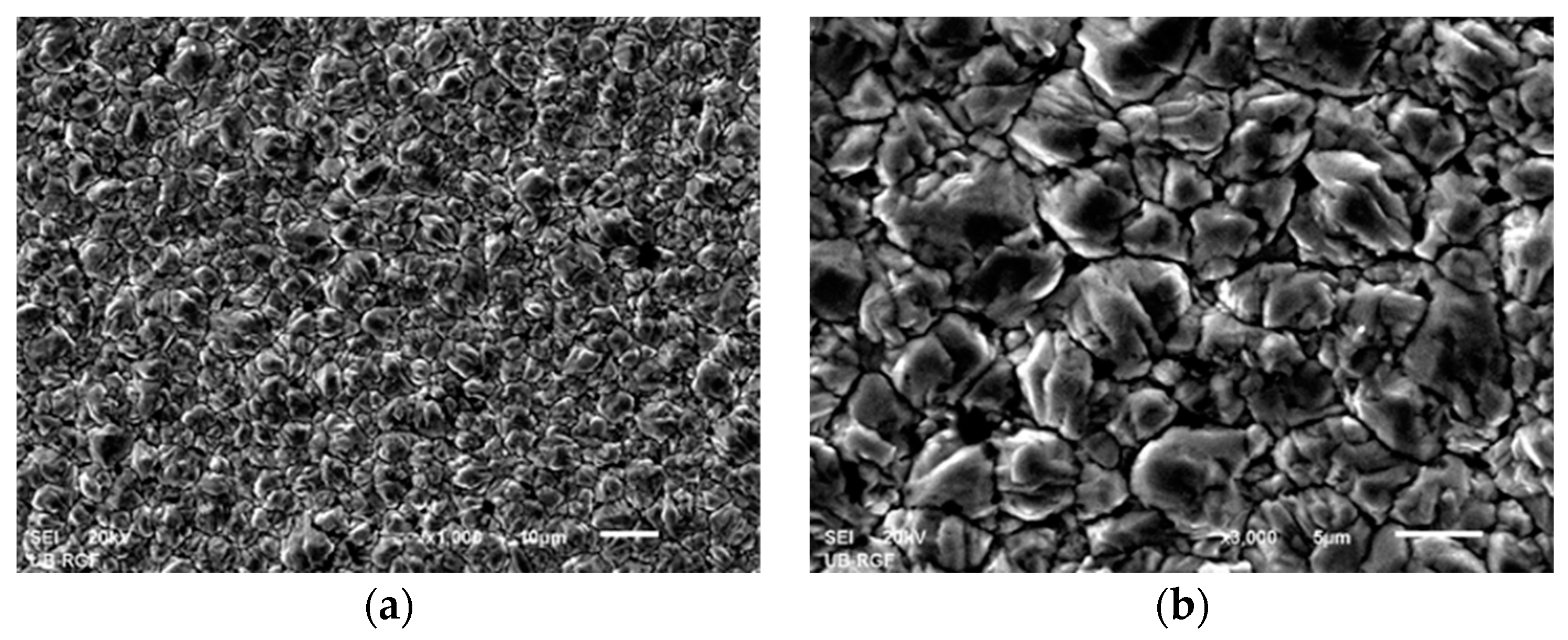
The typical imprint in the Cu coating obtained by Vickers microindentation is shown in Figure 10.
Vickers microindentation belongs to the static method for a determination of hardness of coatings (films). Aside from this static method, there are also the dynamic methods which involve both micro- and nanoindentation [47,48]. Unlike the static method where a determination of coating hardness is based on a measurement of diagonal size of imprint in a coating made by applied load, the dynamic methods are based on continuous processes where the applied load and the displacement of indenter are simultaneously recorded. The nanoindentation method is especially suitable to determine a hardness of thin coatings owing to an avoidance of an influence of substrate with the small applied loads [49].
In order to determine an absolute hardness of any coating, knowledge of hardness of cathode is of crucial importance. The PSR (Proportional Specimen Resistance) model [50] is often used for that purpose, and the values of substrate hardness, Hs were 7.42 GPa for Si(111) [13] and 1.41 GPa for the brass [45].
The following Sub-sections give a survey of the effects of types of both electrolyte and cathode, the thickness of the coating and the electrolyte stirring on hardness of the Cu coatings.

3.1. The Influence of Type of Electrolyte on Hardness of Electrolytically Produced Cu Coatings

The dependencies of the composite hardness, Hc for 20 μm thick Cu coatings produced from electrolyte I and electrolyte II on the brass cathodes on relative indentation depth (RID) are presented in Figure 11a. The RID is given by Equation (2) [12,13,45,51]:
R I D = h δ = d 7 δ
where h is an indentation depth, δ is a coating thickness, and d is a diagonal size, since h = d/7. The effect of cathode hardness in the composite hardness grows with an increase of RID value, i.e., with an increase of a depth of indentation. Although there is no sharp boundary where a substrate commences to effect on a coating hardness, as well as where a composite hardness is being equaled with hardness of a substrate, RID values between 0.1 and 1 are usually considered as boundaries for these influences. The RID zone between 0.1 and 1 is so-called composite zone, and it is a zone where there is strong contribution of cathode hardness to composite hardness. From this reason, for Hc values dominantly situated in this zone, it is necessary to apply the corresponding composite hardness model to determine an absolute hardness of any coating.
The dependencies of Hcoat on RID calculated by C–L model are presented in Figure 11b. It follows that mat coating electrodeposited from electrolyte I had larger both Hc and Hcoat values than mirror bright coating electrodeposited from electrolyte II. The values both measured Hc and calculated Hcoat showed same trend of the dependencies on the RID.
However, it is noticed that for RID values close to 0.1 calculated values of Hcoat were larger than Hc values, whereby the difference between them increased with a decrease of RID value. This illogicity demands an additional analysis in an implementation of the C–L model to obtain real values of hardness of the Cu coatings. It is shown in Figure 11c the dependencies of the (δ/d)m on the RID for the coatings produced from electrolyte I and electrolyte II, where m is a composite Meyer’s index calculated by a linear regression on the way described in Refs. [24,33]. The values of this coefficient are 0.4525 for mat coating electrodeposited from electrolyte I and 0.3423 for mirror bright coating electrodeposited from electrolyte II [12].
The C–L model is valid up to (δ/d)m = 1 [23,24,33,34], and taking this value, it is obtained RID value of 0.14 (Figure 11c). For RID < 0.14, Hc values are smaller than calculated Hcoat values, and the coating hardness is equal to the measured composite hardness. For RID ≥ 0.14, Hc values are larger than Hcoat values, and the coating hardness corresponds to the calculated value. Hence, the RID value of 0.14 is the limiting (or critical) value [(RID)c = 0.14] separating a zone where the measured (composite) hardness is equal to the coating hardness and a zone in which calculated values correspond to the coating hardness.

3.2. The Effect of Type of Cathode on Hardness of Electrolytically Produced Cu Coatings

The dependencies of Hc, Hcoat and (δ/d)m on RID obtained for 20 µm thick Cu coatings produced from electrolyte I and electrolyte II on Si(111) substrate are shown in Figure 12. The values of composite Meyer’s index for these coatings are m = 0.4153 for the coating electrodeposited from electrolyte I and m = 0.3447 for the coating electrodeposited from electrolyte II [12].
It is clear from Figure 12b that the dependencies of the calculated Hcoat on the RID values have opposite trend than those obtained on brass substrate. As seen from Figure 12b, the dependencies of Hcoat–RID have a descending trend. For this system, Hcoat values are considerably larger than Hc values up to RID of 0.14, with a tendency of a decrease of this difference with an increase of RID value. After RID value larger than 0.14, the Hcoat values become smaller than Hc values, confirming that this value is the limiting or critical one after which an application of the C–L model was necessary for a determination of an absolute hardness of the Cu coatings.

3.3. The Effect of the Coating Thickness on Hardness of Electrolytically Produced Cu Coatings

Figure 13 shows the dependencies of Hc, Hcoat and (δ/d)m on RID for 40 µm thick Cu coatings obtained by the electrodeposition from electrolyte I and electrolyte II on Si(111) substrate. The values of Meyer’s parameters are m = 0.4290 for the Cu coating electrodeposited from electrolyte I and m = 0.3367 for the Cu coating electrodeposited from electrolyte II [12].
The dependencies of Hc and Hcoat on RID values have the same trend as those obtained for 20 µm thick Cu coatings on the same substrate (Figure 12). The only difference is a shift of hardness values towards lower RID values, i.e., towards the zone of equalized composite (measured) and coating hardness. For this case, the RID value of 0.14 was confirmed as the limiting value separating a zone where the coating hardness is equal to the composite (measured) hardness than a zone where it is necessary to apply the C–L model to determine an absolute hardness of the Cu coatings.

3.4. Influence of Electrolyte Stirring on Hardness of Electrolytically Produced Cu Coatings

Figure 14 shows the dependencies of Hc, Hcoat and (δ/d)m on RID obtained by the electrodeposition from electrolyte I on the brass substrate with various intensities of imposed ultrasound. The values of coefficient m for the considered coatings are given in Table 2.
The dependencies of values of Hc and Hcoat on RID have „S“ shape, as seen from Figure 14a,b. Both of the hardness values grow with an increase of RID values up to about 0.40. Then, their sharp decrease commences up to the value corresponding approximately to a hardness of the brass cathode, Hs, of 1.41 GPa [45]. For these coatings, the limiting or critical RID value of 0.14 (Figure 14c) separating the two zones is also confirmed.
The dependencies of Hc, Hcoat and (δ/d)m on RID obtained for the Cu coatings produced from electrolyte II on the brass with various intensities of imposed ultrasound are shown in Figure 15. The values of m coefficients for the considered coatings are given in Table 2.
The values of both Hc and Hcoat increased with the increase of RID value, approaching to value corresponding to hardness of the brass cathode (Figure 15a,b). Certainly, the “S” shape of these dependencies is not obtained, probably due to lower values of both Hc and Hcoat relative to the coatings electrodeposited from electrolyte I. The limiting RID value of 0.14 was also observed for the coatings electrodeposited in the presence of leveling/brightening addition agents under imposed ultrasound of various intensities.

4. Influence of Parameters of the PC Regime on Morphology and Structure of Electrolytically Produced Cu Coatings

Electrodeposition by pulse reverse current (PRC) regimes offers many benefits in obtaining metal deposits of desired characteristics. The deposits obtained by these regimes usually possess both lower porosity and more compact structure than the deposits produced by the constant regimes of electrodeposition. The development of electronic industry lowers a price of pulse rectifiers, that is still incomparable higher than the DC units [52], and this lowering of price enables larger application of pulse reverse regimes in commercial purposes. The only pulsating (PC) and reversing current (RC) regimes have potential commercial application from all PRC regimes of the electrodeposition.
The PC regime is defined by the average current density (jav), the current density amplitude (jA), a deposition pulse (tc) and a period of pause (tp) on way given by Equation (3) [8]:
j av = j A t c t c + t p
Since the pause-to-pulse ratio, p is defined by Equation (4) [8]:
p = t p t c
The average current density (jav) is also defined by Equation (5):
j av = j A 1 + p
The frequency, ν is defined by Equation (6):
ν = 1 t c + t p
The pulsating current regime gives optimal results in the millisecond range, in the (10–100) Hz frequency range [8]. In this range of frequency, the surface concentration of depositing ions is constant and corresponds to a concentration in the constant DC regime at the current density equal to the average current density in regime of the pulsating current [8,53]. It means that electrochemical deposition in the PC regime in this frequency range takes place at the average current density.
The regime of reversing current (RC) includes anodic component of the current density, and instead of pause duration, the anodic time is included [8].
In this review paper, influence of the following parameters of electrodeposition and the pulsating current regime on morphology, structure and hardness of the Cu coatings is analyzed [13,45,46]:
(1) the average current density, jav or frequency, ν—these parameters are analyzed keeping constant the current density amplitude and the deposition pulse, while pause duration is varied,
(2) the current density amplitude, jA—these parameters are analyzed keeping constant both deposition pulse and pause duration,
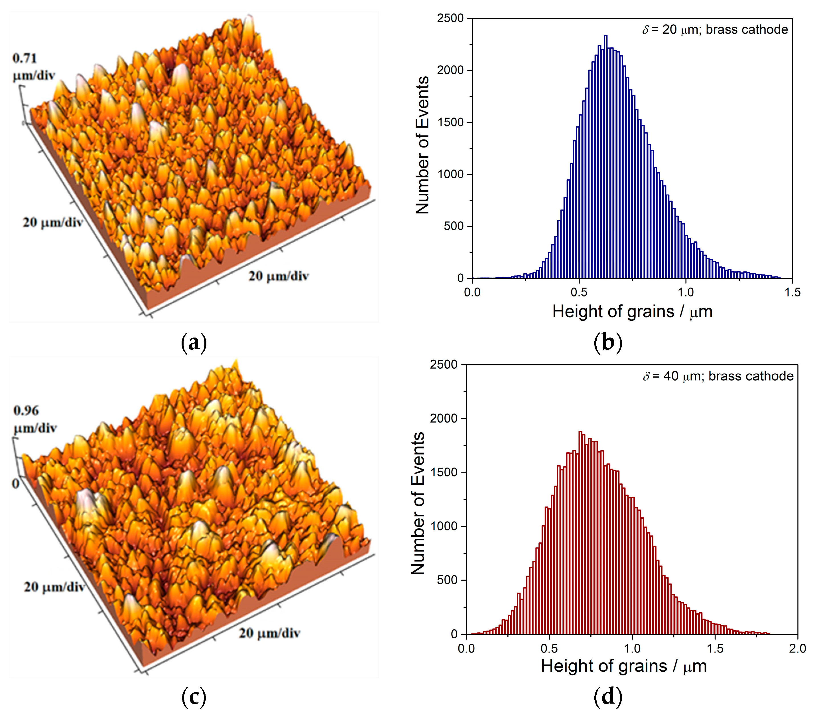
(3) coating thickness, δ—coating thickness is varied keeping the parameters of pulsating current regime constant (the current density amplitude, the deposition pulse, and the pause duration), and
(4) type of cathode.
The parameters of the pulsating current regime analyzed in this review paper are summarized in Table 3.

4.1. Influence of the Average Current Density (or Frequency) on Morphology and Structure of the Cu Coatings

Figure 16 shows the Cu coatings produced at jav of 15 (Figure 16a,b), 25 (Figure 16c,d), 40 (Figure 16e,f) and 50 mA cm−2 (Figure 16g,h) on the Si(111) electrode. All Cu coatings presented in Section 4 were electrodeposited from electrolyte I at a temperature of 22.0 ± 0.50 °C without electrolyte stirring.
The size of grains decreased with an increase of the average current density (or frequency) from 15 to 50 mA cm−2 (i.e., from 30 to 100 Hz). The well-defined grains size about 10 μm are mostly formed at 15 mA cm−2 (30 Hz). The number of grains of this size decreased with increasing the average current density, in order to size of grains in the coatings produced at 40 and 50 mA cm−2 (80 and 100 Hz) was predominant about or below 5 μm [13].
The topography and the histograms of the shown Cu coatings are presented in Figure 17a,c,e,g—AFM images; Figure 17b,d,f,h—histograms.
The Ra roughness values for the coatings are given in Table 4, from which can be seen that the coating roughness decreases with the increase of the average current density.
The XRD analysis of 40 µm thick Cu coatings produced by various PC regimes is shown in Figure 18. The shown diffractograms represent typical diffractograms of Cu with 2θ angles of 43.3°, 50.4°, 74.1° and 89.9° corresponding to the (111), (200), (220) and (311) crystal planes.
The values of TC(hkl) and RTC(hkl) coefficients for given the Cu coatings are summarized in Table 5 and Table 6.
The Cu coating produced at jav of 15 mA cm−2 (or ν of 30 Hz) exhibited the strong (220) preferred orientation. With an increase of jav (or ν), the share of crystallites oriented in this plane decreased, and crystallites of Cu become predominately oriented in (311), (111) crystal planes [13].

4.2. Influence of the Current Density Amplitude on Morphology and Structure of the Cu Coatings

Figure 19 shows the Cu coatings produced with the current density amplitudes, jA of 120 (Figure 19a,b) and 140 mA cm−2 (Figure 19c,d). These current density amplitudes corresponded to jav of 60 and 70 mA cm−2, since values tc and tp are kept constant (tc = tp = 5 ms).
The size of grains in the Cu coating electrodeposited with jA of 120 mA cm−2 (jav = 60 mA cm−2) was about 5 µm or less, and this coating was very similar to those produced with jav of 40 and 50 mA cm−2 (Figure 16e–h). The further increase in jA (or jav) led to formation of globules size of about 30 µm (Figure 19c).
The 3D AFM images and the histograms of the topography of the Cu coatings obtained with the current density amplitudes of 120 and 140 mA cm−2 are shown in Figure 20 (Figure 20a,b for the coating obtained with jA of 120 mA cm−2 and Figure 20c,d with jA of 140 mA cm−2).
The Ra roughness values of these coatings were 237 ± 2.2 nm for the Cu coating produced with jA of 120 mA cm−2, and 229.1 ± 2.2 nm for that produced with jA of 140 mA cm−2. The obtained values were slightly higher than that obtained for coating produced with jA of 100 mA cm−2 under the same all other parameters of the PC regime (Figure 16g,h). It is necessary to note that the deposit among globules was analyzed in the coating electrodeposited with jA of 140 mA cm−2.
The XRD analysis (Figure 21) revealed a strong influence of the current density amplitude on the preferred orientation of the produced Cu coatings. Please note that the diffractogram shown in Figure 18 for ν of 100 Hz (jA = 100 mA cm−2) is repeated in Figure 21.
Analysis of TC(hkl) and RTC(hkl) coefficients given in Table 7 showed that Cu crystallites were mostly oriented in (111) crystal plane, and that a share of crystallites oriented in this plane increased with an increase of the current density amplitude. Generally, the increase of jav from 15 to 70 mA cm−2 (Figure 16 and Figure 19, Table 5, Table 6 and Table 7) causes a change of the preferred orientation of the Cu coatings from the strong (220) to the strong (111) preferred orientation.

4.3. Influence of the Coating Thickness on Morphology of the Cu Coatings

Figure 22 shows the 3D AFM image and the histogram of topography of 20 µm thick Cu coating produced at jav of 50 mA cm−2. The other parameters of PC regime are jA = 100 mA cm−2, tc = tp = 5 ms.
The value of Ra roughness for this coating was 101.5 ± 1.9 nm. By insight in Table 4, and comparing the values obtained for the same PC regime, it follows that similar to the DC regime, an increase of the electrodeposition time, i.e., the coating thickness causes an increase of the coating roughness.

4.4. Influence of the Type of Cathode on Morphology of the Cu Coatings

Figure 23 gives morphology of 40 µm thick Cu coating produced by the pulsating current regime at jav of 50 mA cm−2 (jA = 100 mA cm−2; tc = tp = 5 ms) on the brass cathode. At the macro level, this coating was very similar to that obtained on the Si(111) electrode with the same PC parameters (Figure 16g,h). The grains of size of about 5 µm are mostly electrodeposited on this cathode.
The 3D AFM images and the histograms of topography of 20 and 40 µm thick coatings of Cu produced on brass cathode at jav of 50 mA cm−2 are shown in Figure 24 (20 µm, Figure 24a,b and 40 µm, Figure 24c,d).
The Ra roughness values were 146.0 ± 1.8 nm for 20 µm, and 215.6 ± 2.2 nm for 40 µm thick coatings of Cu [45]. These values were higher than those obtained on the Si(111) substrate, that can be ascribed to, similar to the Cu coatings electrodeposited in the DC regime, higher initial roughness of the brass than the Si(111) cathodes.

5. Influence of Parameters of the PC Regime on Hardness of Electrolytically Produced Cu Coatings

Figure 25 shows the dependencies of the Hc, Hcoat, (δ/d)m on the RID for 40 µm thick Cu coatings produced by the PC regime from electrolyte I at frequencies of 30, 50, 80 and 100 Hz, i.e., at average current densities of 15, 25, 40 and 50 mA cm−2 [13,54].
The m coefficient values for these coatings are given in Table 8 [13,54].
It follows from Figure 25b that the calculated Hcoat values have typical descending trend of a change with the increase of RID values characteristic for Si(111) substrate. At the small RID values, the Hcoat values were notably larger than the measured Hc values, and this difference decreased with an increase of RID value. For RID ≥ 0.14, the measured hardness became larger than the calculated coating hardness. Taking into consideration the validity of the C–L model up to (δ/d)m = 1 [23,24,33,34], it is confirmed the limiting (or critical) RID value of 0.14 separating the zone where the measured hardness is equal to the coating hardness from the zone where an application of the C–L model is necessary to obtain the absolute coating hardness.
This limiting RID value of 0.14 is also confirmed for the Cu coatings obtained with different the current density amplitudes, and it is also valid for the Cu coatings of different thicknesses produced by the PC regime [54]. Figure 26 shows the dependencies of the Hc, Hcoat, (δ/d)m on the RID for 40 µm thick Cu coatings obtained by the pulsating current regime with the current density amplitudes, jA of 120 and 140 mA cm−2 (or jav of 60 and 70 mA cm−2, respectively), and for 20 µm thick Cu coating electrodeposited at jav of 50 mA cm−2 (see Table 3). The m coefficient values for the Cu coatings electrodeposited at jav of 60 and 70 mA cm−2 are presented in Table 8, while m value for 20 µm thick Cu coating was 0.3591 [13,54].
The effect of the kind of cathode on hardness of electrolytically produced Cu coatings is examined through analysis of the Cu coatings produced by the pulsating current regime on the brass substrate. Figure 27 shows the dependencies of the Hc, Hcoat, (δ/d)m on RID for 20 and 40 µm thick Cu coatings electrodeposited on the brass substrate at jav (jA) of 50 mA cm−2 (100 mA cm−2). The m coefficient value for 20 µm thick coating is 0.4141, and 0.3744 for 40 µm thick coating [45].
According to expectation, the dependencies of Hc and Hcoat on RID were very similar to each others (Figure 27a,b). The Hc and calculated Hcoat values approached to a hardness of brass substrate at the high RID. At the low applied loads, Hcoat were larger than Hc whereby the differences between Hc and Hcoat were smaller than on Si(111) cathode. The validity of the C–L model ((RID)c = 0.14 for (δ/d)m = 1; Figure 27c) is confirmed for the Cu coatings electrodeposited by the PC regime on the brass cathode.

6. Correlation among Morphology, Structure and Hardness of Electrolytically Produced Copper Coatings

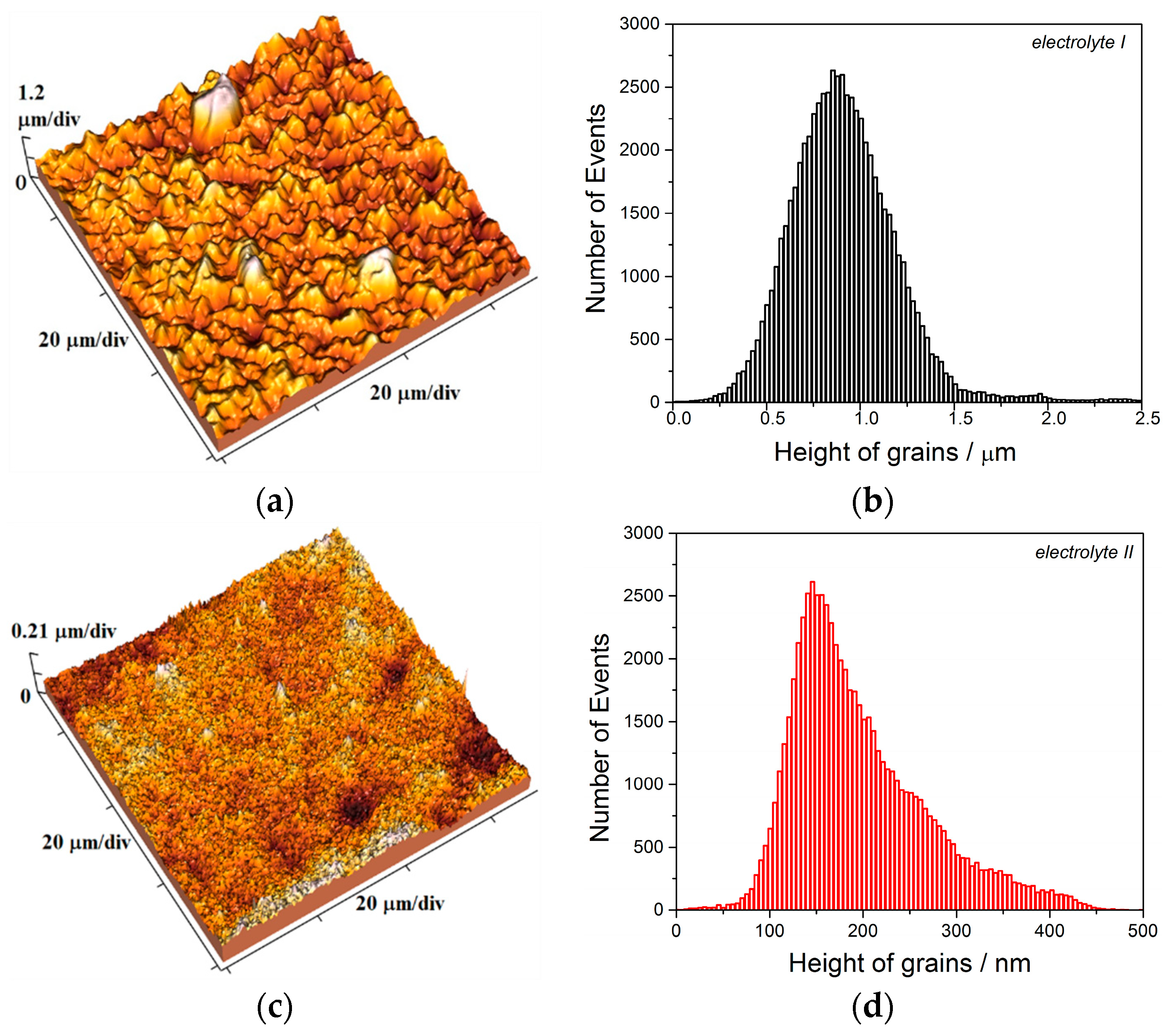
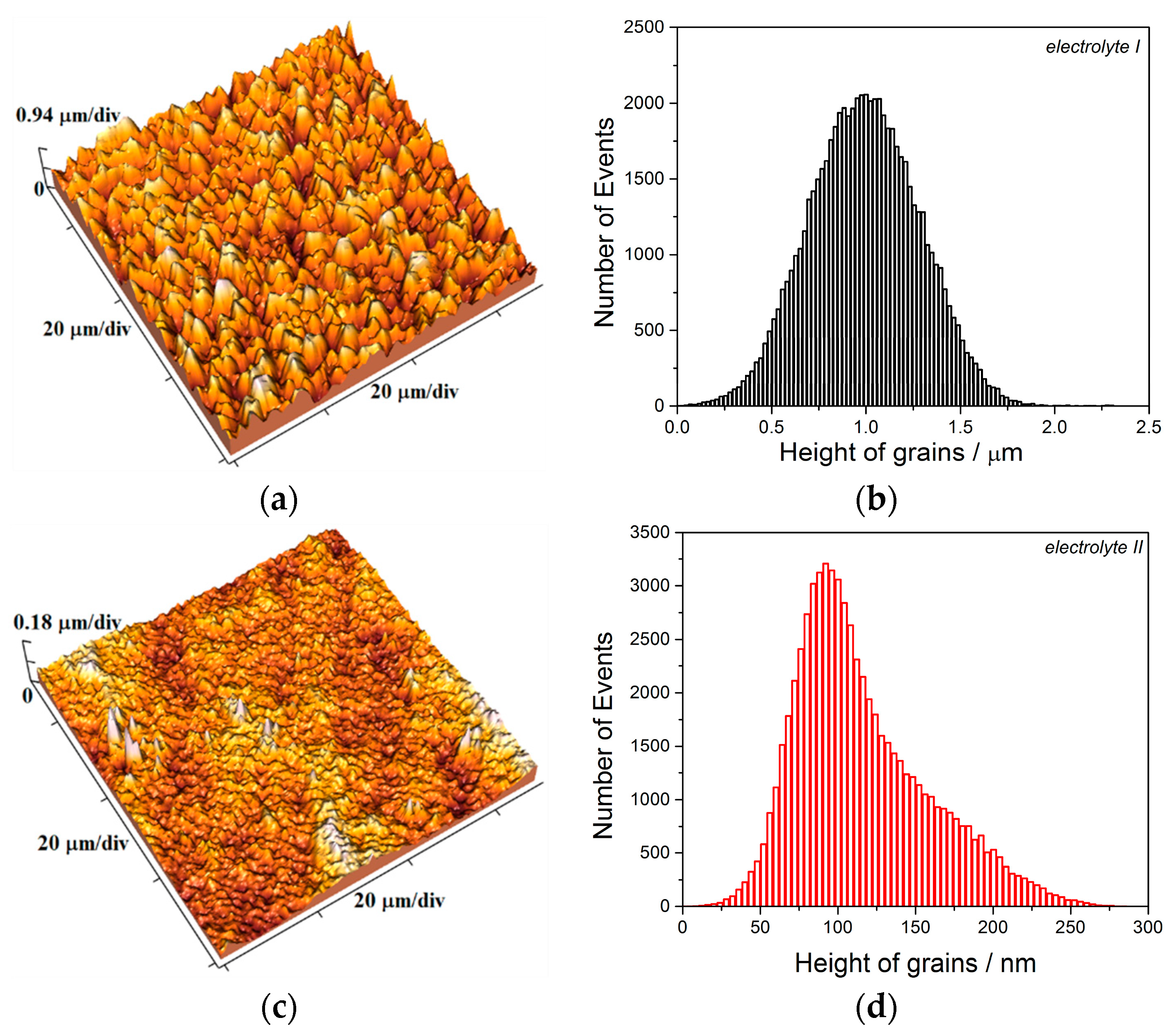
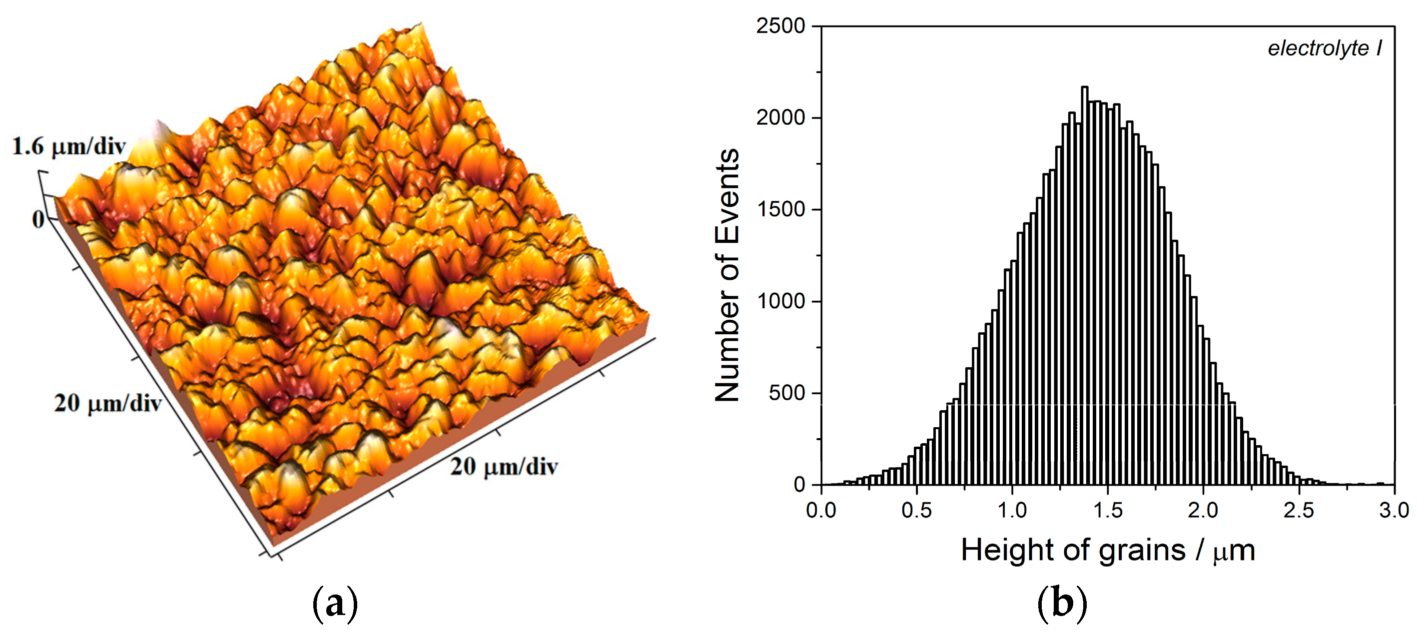
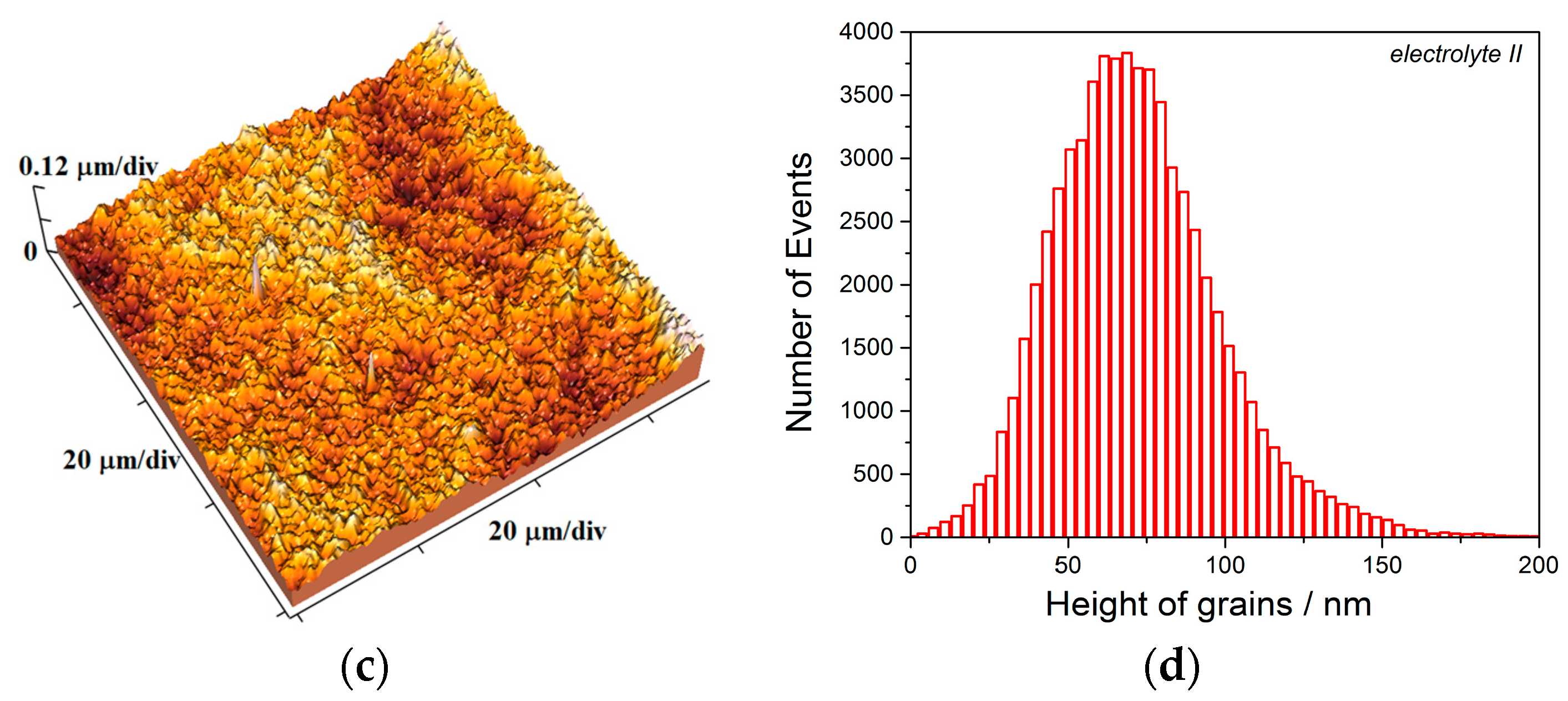
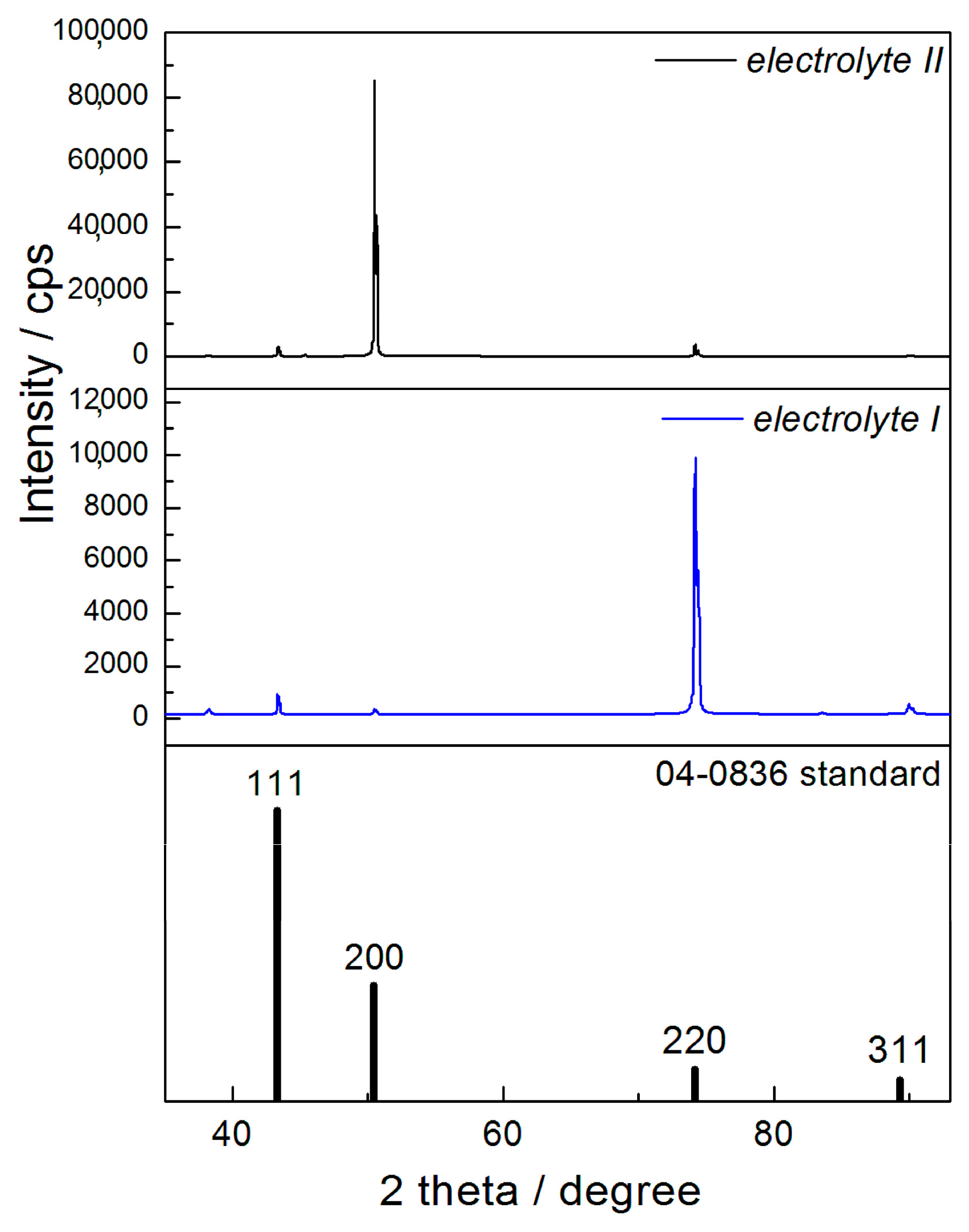
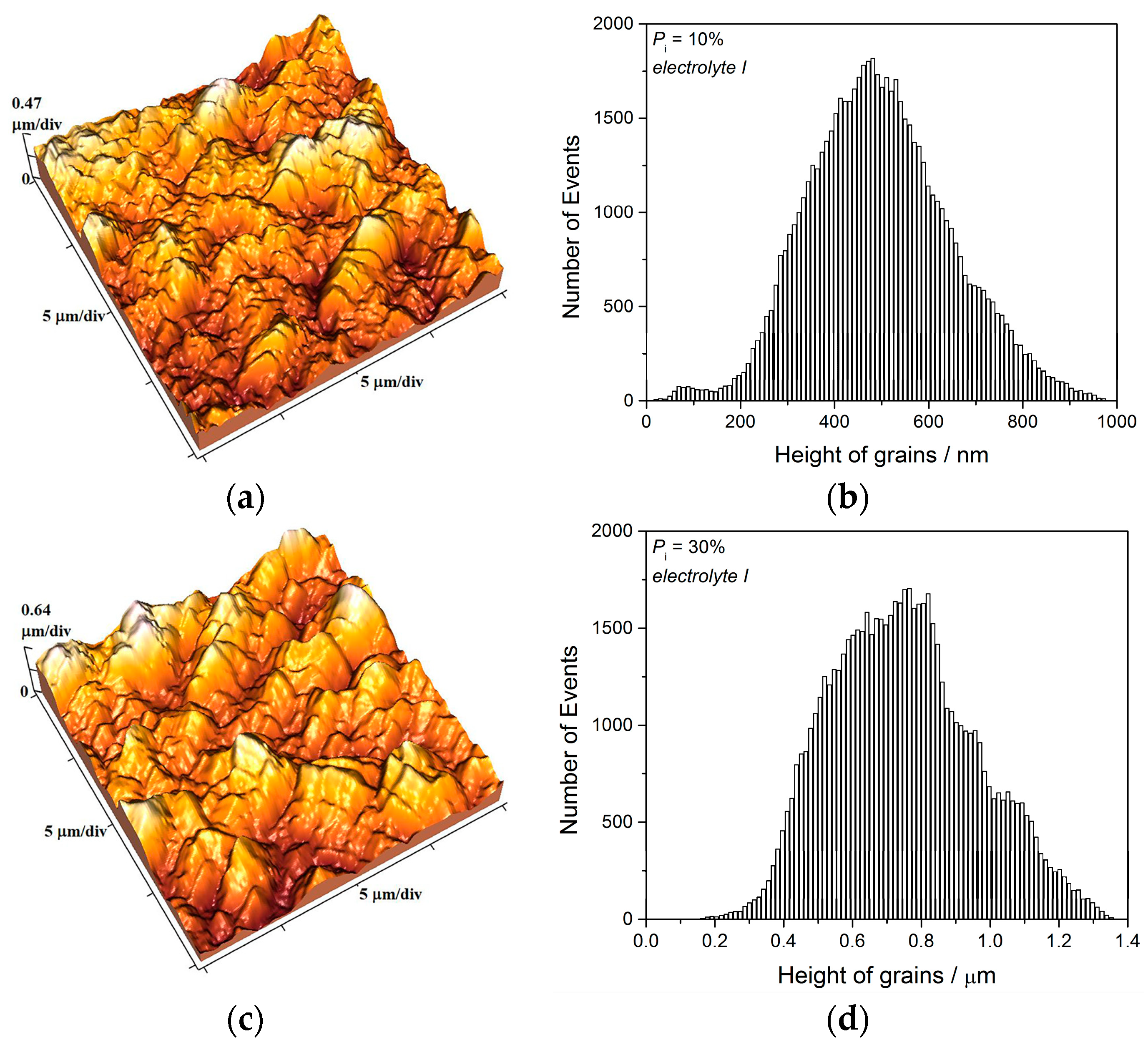
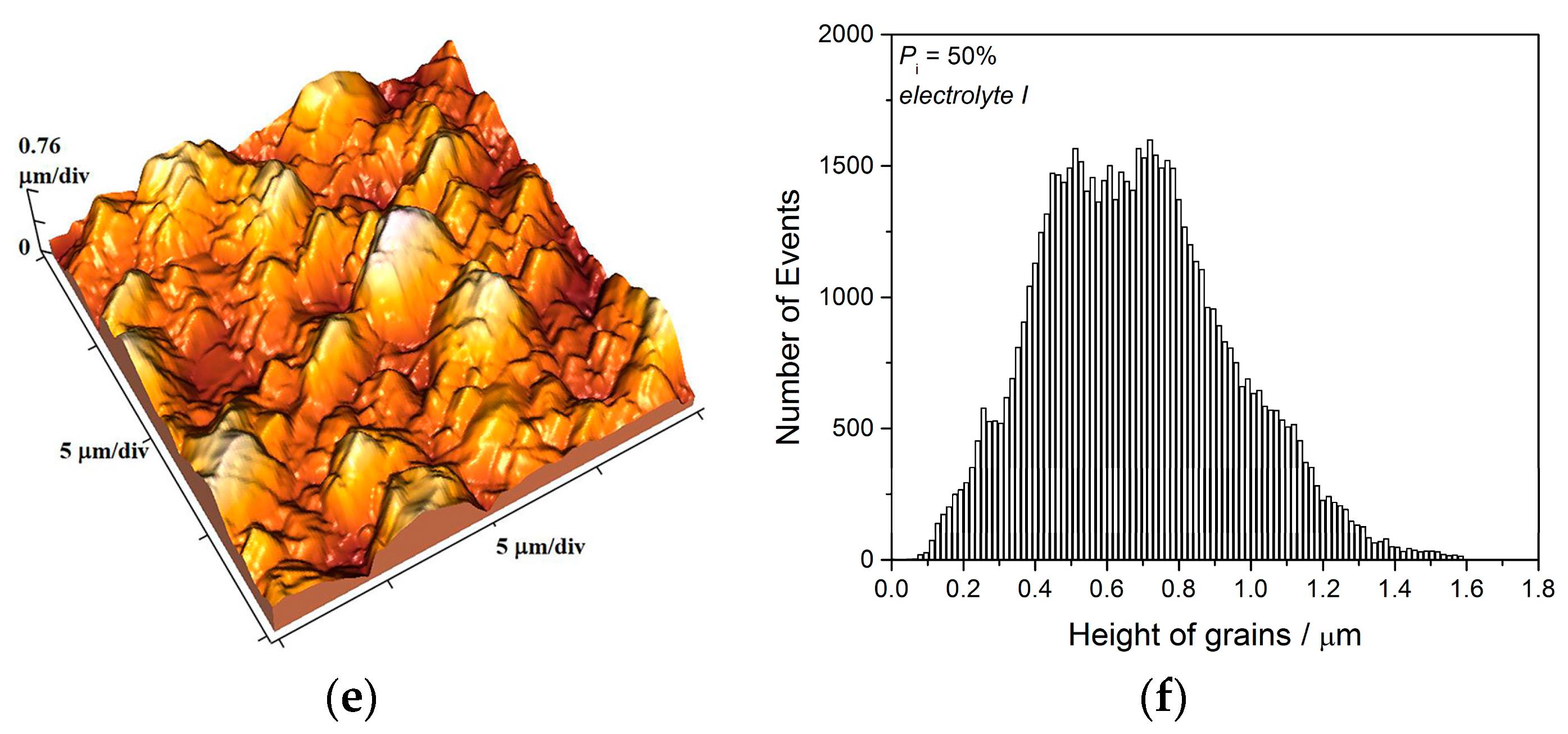
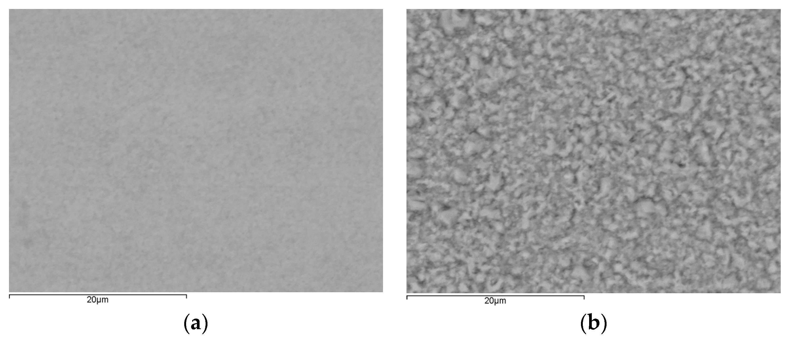
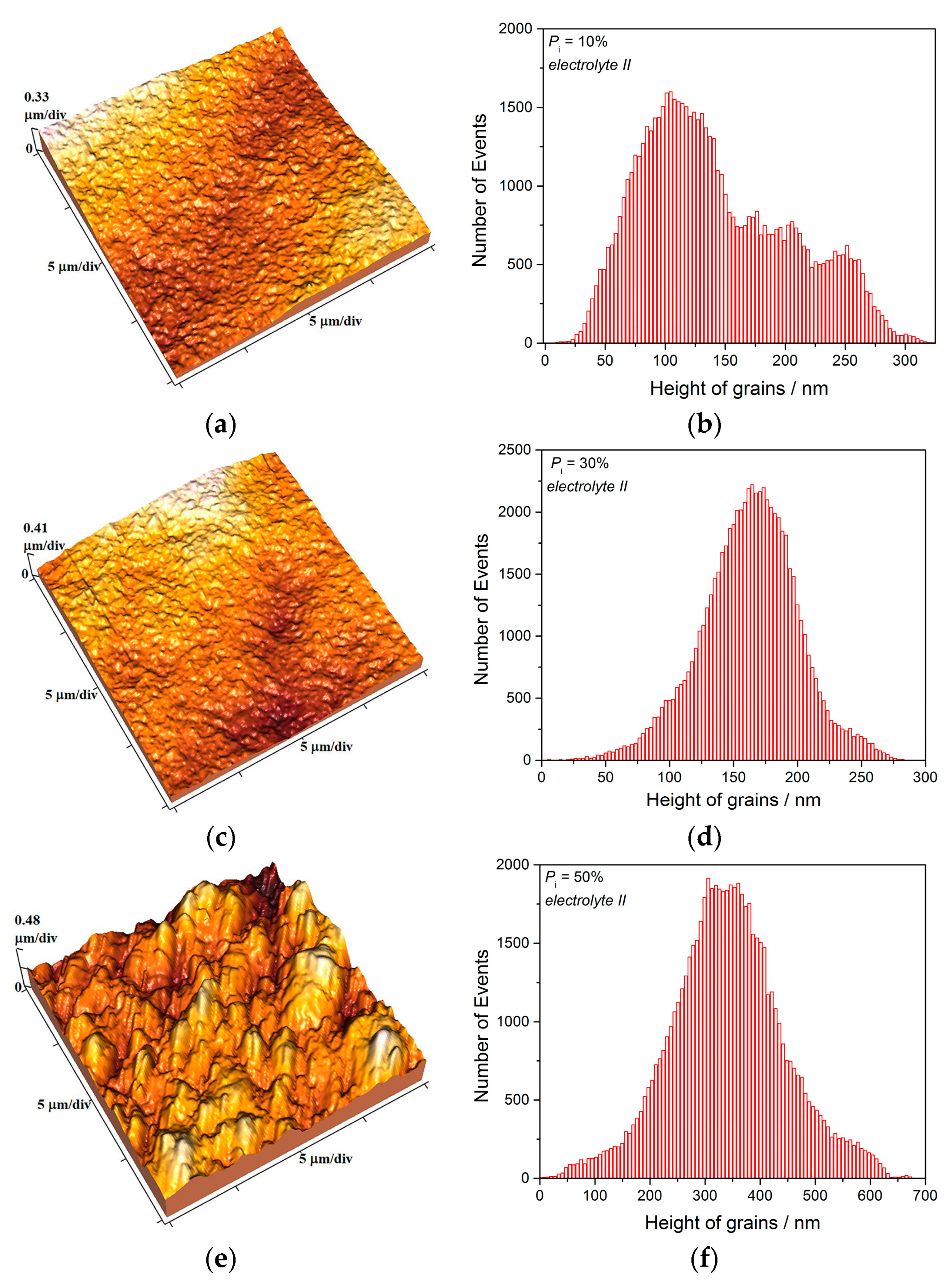
The two kinds of compact and uniform Cu coatings were obtained by electrodeposition in the DC regime. The fine-grained mat coatings are produced from the basic sulfate electrolyte (electrolyte I), and the very smooth mirror bright coatings from the electrolyte in the presence of additives for leveling and brightness (electrolyte II). The analysis of histograms confirmed the strong difference between them. In the mat Cu coatings, the grain heights are at the micro level, while in mirror bright Cu coatings the grain heights were at the nano level. The addition of the additives affected not only morphology of the coatings, but to crystal structure of the produced coatings. The mirror bright Cu coatings exhibited the strong (200) preferred orientation, while those produced from the basic sulfate solution exhibited the strong (220) preferred orientation.
The change in morphology and structure of the Cu coatings can be attributed to a synergistic effect of the used leveling/brightening addition agents on electrodeposition of copper. The adsorbed chloride layer is formed on electrode surface by an addition of small concentrations of chloride ions (1−10 mM). This adsorbed layer mediates copper reduction and introduces an additional reaction pathway, resulting in an overall depolarization of the reduction process. Both depolarization and the increase in peak current observed in the cyclic voltammograms (CVs) revealed a catalytic effect of chloride on Cu reduction [55]. PEG is copolymer and nonionic surfactant, acting as a suppressor of the electrodeposition process only in the presence of chloride ions [56]. There is no unique mechanism explaining adsorption/suppression effect of PEG in the presence of chloride ions on Cu electrodeposition process. The various mechanisms are proposed and they are summarized in Ref. [56]. The MPSA is top brightening addition agent added in parts per million (ppm) concentrations to acid sulfate Cu electrolytes [56,57]. The addition of this additive to the basic sulfate electrolyte with already added chloride/PEG additives activates electrodeposition process enabling a formation of mirror bright coatings [10,11,57]. The typical model explaining synergistic effect of this combination of additives causing a formation of mirror bright coatings is known as the model of “local perforation” [58,59].
The electrolyte stirring is another important parameter of the electrodeposition affecting a quality of metal coatings, whereby a quality of the coating is strongly influenced by intensity of stirring of the electrolyte. The various intensity of electrolyte stirring can be imposed by application of ultrasound of various powers, and it can be considered as follows: the compact and uniform Cu coatings are produced at the current density, j of 50 mA cm−2 which belongs to the mixed activation-diffusion control of the electrodeposition process.
For this type of electrodeposition control, the overpotential of electrodeposition can be presented by Equation (7) [8,60]:
η = b c 2.3 ln j j 0 + b c 2.3 ln 1 1 ( j / j L )
where: bc is the cathodic Tafel slope, j0 is the exchange current density and jL is the limiting diffusion current density.
The first term, ηact
η act = b c 2.3 ln j j 0
is an activation part of overpotential required for the charge transfer, and the second term, ηdiff
η diff = b c 2.3 ln 1 1 ( j / j L )
is a diffusion part of overpotential and it is due to mass transfer limitations (diffusion limitation primarily).
Ultrasound imposed to the electrodeposition process only effects on the diffusion part of overpotential. The imposed ultrasound causes a mixing of the solution in the near-electrode layer, causing the decrease of the diffusion layer thickness, and the increase of the limiting diffusion current density. The degree of the diffusion control in the mixed activation-diffusion control decreases (i.e., it decreases the diffusion part in Equation (7)) by electrolyte stirring, and this decrease enhances with an intensification of electrolyte stirring.
The effect of imposed ultrasound is equivalent to the other ways of electrolyte stirring, such as imposed magnetic field and magnetic stirring [60,61], but also to vigorous hydrogen evolution occurring parallel to metal electrochemical deposition [62]. The concept of „effective overpotential“ originally proposed to explain a change of the hydrodynamic conditions in the near-electrode layer caused by vigorous hydrogen evolution [
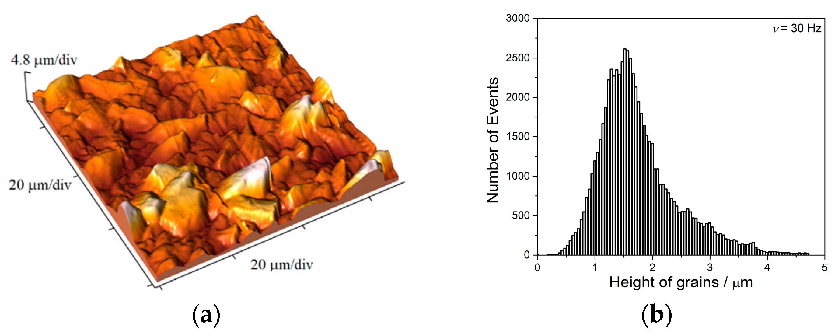
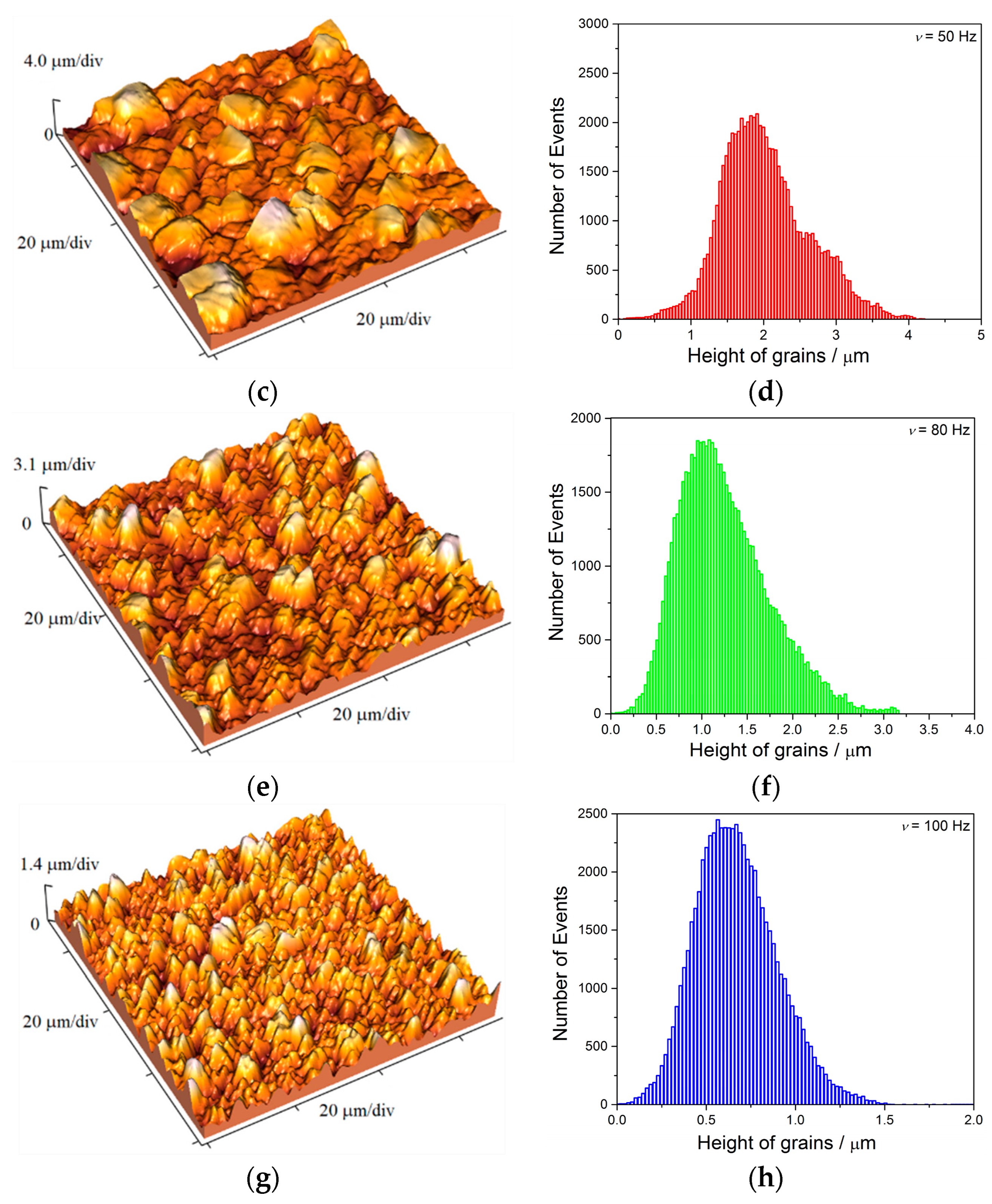
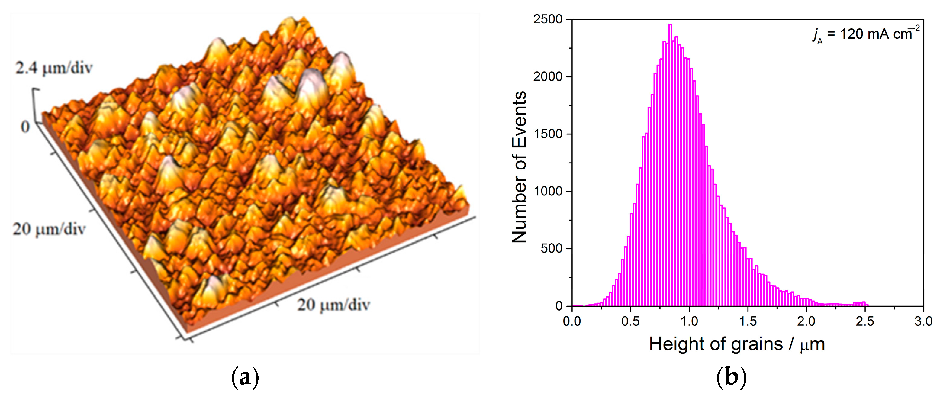
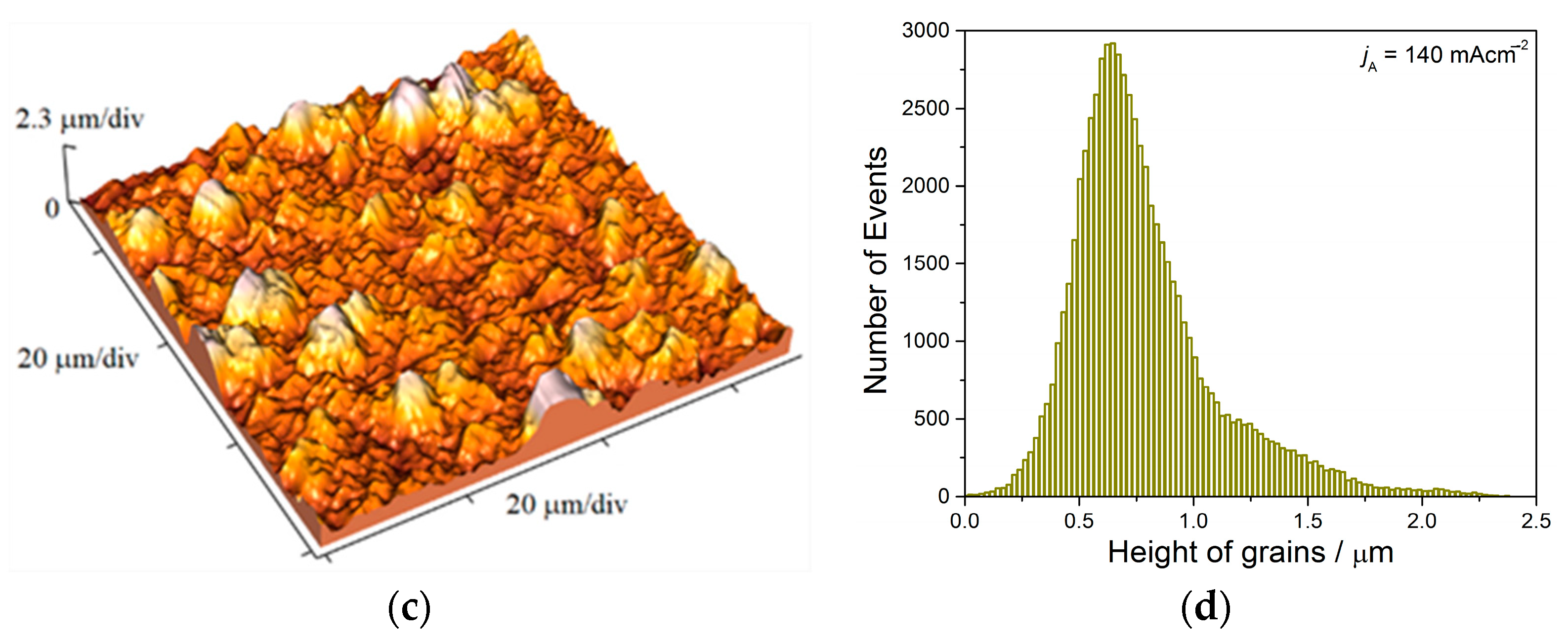
62] is applicable for all other ways of electrolyte stirring. The production of different morphologies of the Cu coatings under different intensities of applied ultrasound (Figure 6, Figure 7, Figure 8 and Figure 9) can be considered as follows: the solution stirring in the near-electrode layer intensifies with an increase of the intensity of imposed ultrasound. As a result of this intensification, the degree of the diffusion control in the mixed activation-diffusion control decreases. Since the activation part is independent of the electrolyte stirring, it means that the contribution of the activation control in the mixed activation-diffusion control increases with an increase of the intensity of ultrasound. This causes a formation of large and regular crystal grains in the coatings produced under strong imposed ultrasound (see parts in circles in Figure 6b). Namely, formation of regular and well defined grains is result of dominant activation control in the overall control of the electrochemical deposition process [8].
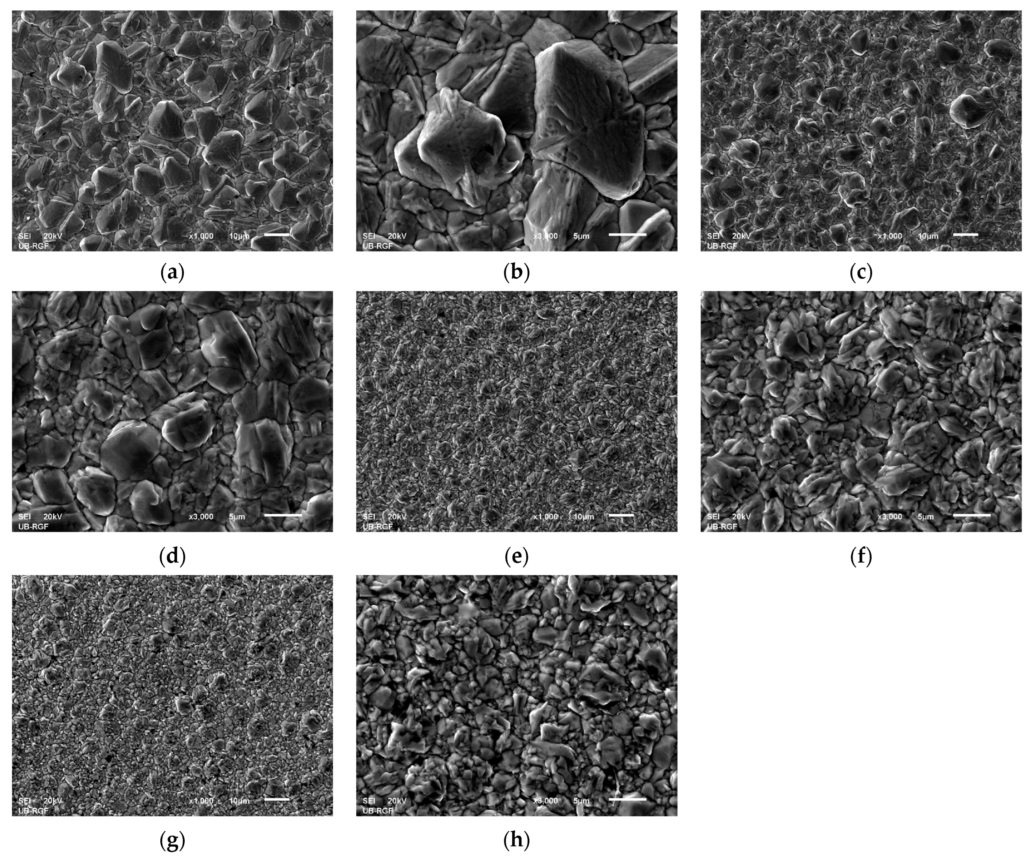
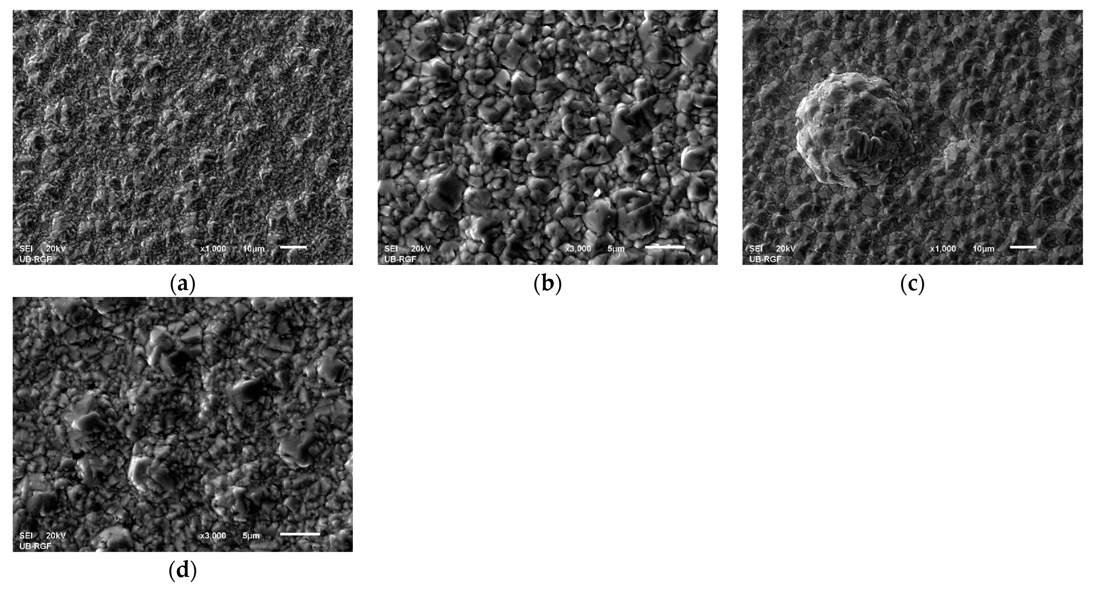
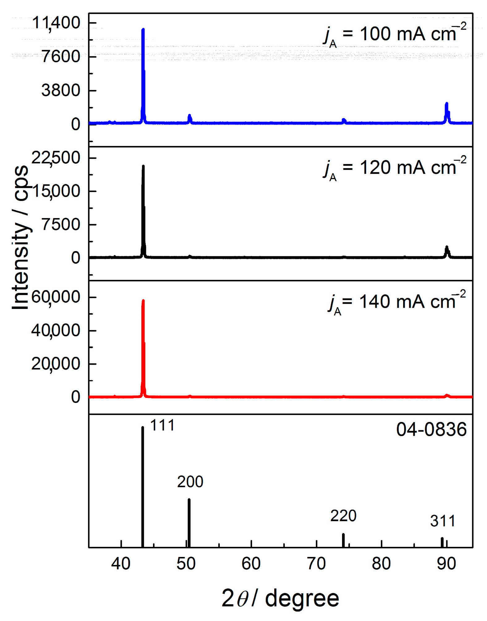
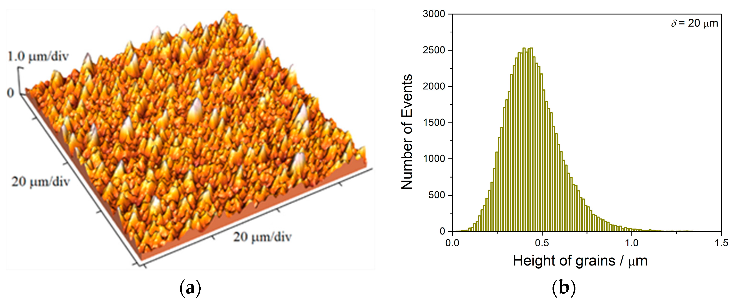
The equivalent effect on morphology and structure of electrodeposited Cu coatings is achieved by the pulsating current regime. The range of the average current densities between 15 and 70 mA cm−2 belongs to the mixed activation-diffusion control of the electrochemical deposition process [13]. With the increase of the average current density, the share of the activation control decreased, while the share of diffusion control increased in the mixed activation-diffusion control of the electrochemical deposition. The regular and well defined grains formed with jav of 15 mA cm−2 (Figure 16a,b) are characteristic of predominant activation control, while globules are formed with jav of 70 mA cm−2 (Figure 19c) when diffusion becomes predominant process in the mixed activation-diffusion control of electrochemical deposition.
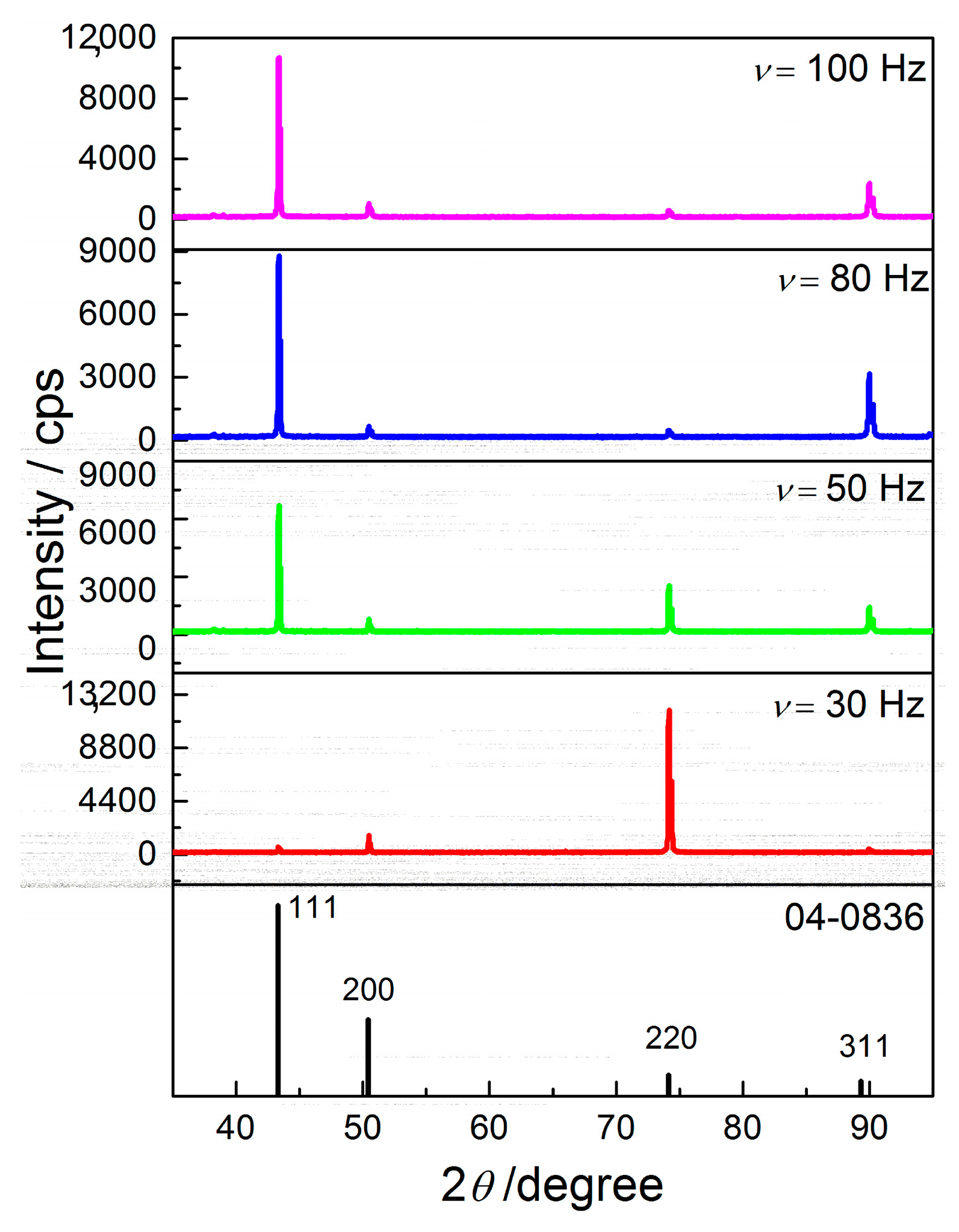
The change in coating morphology is accompanied by change of the preferred orientation from the strong (220) to the strong (111) preferred orientation with the increase of jav value. This change of the preferred orientation can be explained by different growth rate on different crystal planes [63]. The rates of growth are associated with the surface energy values of crystal planes γ and for the FCC type of crystal lattice following the trend γ111 < γ100 < γ311 < γ110 [64,65]. Following the values of surface energy, the electrodeposition rate is the smallest on the (111) crystal plane, and for that reason, the (111) plane represents “slow-growing crystal plane” surviving the electrochemical deposition process [66]. All other crystal planes, i.e., (100), (311) and (110) planes, are the “fast-growing crystal planes” and they disappear firstly during electrochemical deposition process. In this case, with an intensification of the electrodeposition process, i.e., with increasing the average current density from 15 to 70 mA cm−2, it increases a share of Cu crystallites oriented in the (111) crystal plane, while it decreases a share of crystallites in all other crystal planes, especially in (220) crystal plane (Figure 18 and Figure 21, and Table 5, Table 6 and Table 7).
The mat Cu coatings produced from the basic sulfate electrolyte (electrolyte I) showed larger coating hardness than mirror bright Cu coatings produced in the presence of leveling/brightening additives (electrolyte II). The processes occurring on boundary among grains are responsible for this difference [12]. Namely, mat coatings have fine-grained structure with numerous boundaries among grains. The boundaries among grains are a disruption sites for a dislocation motion, and they prevent a movement of the dislocations [46,67]. It can be said that the boundaries among grains behave as mini resistors which resist during indentation in the metal coating. On the other hand, mirror bright Cu coatings were very smooth, without clear boundary among grains, and dislocation motion is a dominant mechanism affecting the coating hardness.
Analysis of histograms for the coatings electrodeposited from electrolyte I by both DC and PC regimes clearly revealed their microcrystalline (mc) character, and for them, Hall-Patch equation [68] predicting an increase of coating hardness with a decrease of grain size is valid. On the other hand, the histogram analysis of smooth mirror bright coatings revealed their nanocrystalline (nc) character with size of grains below critical value for a validity of Hall-Patch equation, and for these coatings, the inverse Hall-Petch equation begins to hold [69].
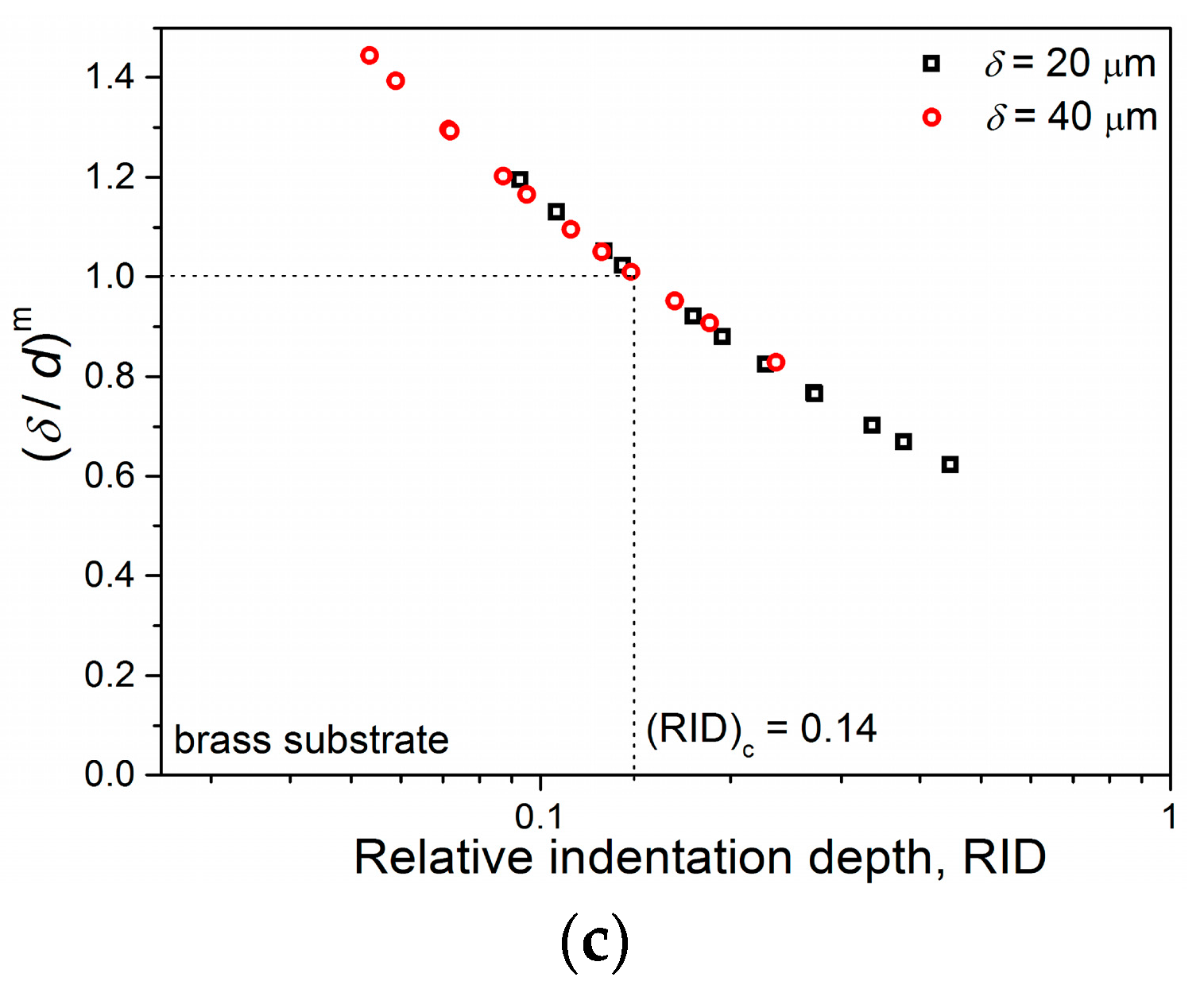
The values of both composite and calculated coating hardness on Si(111) were larger than the values obtained on the brass cathode, what clearly indicate that a determination of coating hardness is complex phenomena depending on many factors, such as the indenter geometry, plastic pile-up effect, film/substrate adhesion, elastic properties of the film and substrate and the friction between the indenter and film [70,71,72,73,74,75,
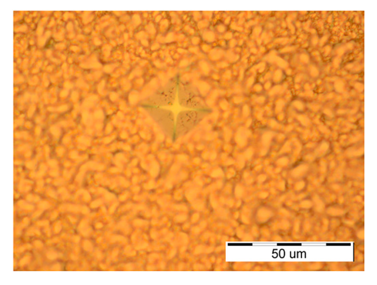
76]. The pile-up effect affecting the coating hardness value can be the easiest looked at through analysis of the Cu coatings electrodeposited from electrolyte I and electrolyte II, as seen from 
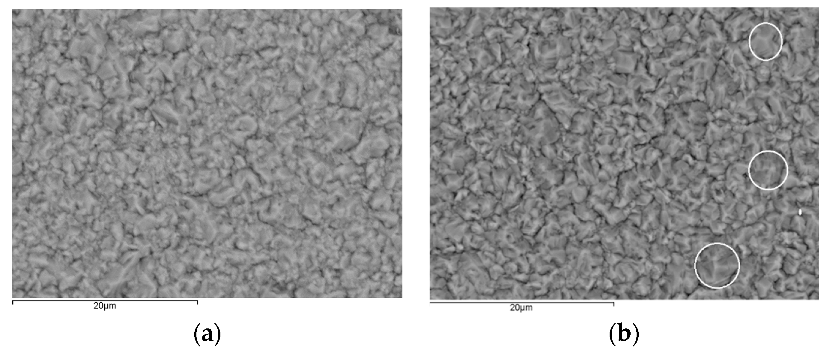
Figure 28 showing Vickers indents.
In the Cu coating electrodeposited from electrolyte I, the main mechanism is a plastic deformation of the coating under the indenter (Figure 28a) [18]. The plastic deformation of fine-grained coatings produced from electrolyte I occurs throughout the grain with the slip of dislocations mostly in the grain interior (intragranular slip) [77]. In the nanocrystalline coatings electrodeposited from electrolyte II, a pile-up effect occurs at edge of the indent (Figure 28b), and this effect is not observed in the Cu coating electrodeposited from electrolyte I.
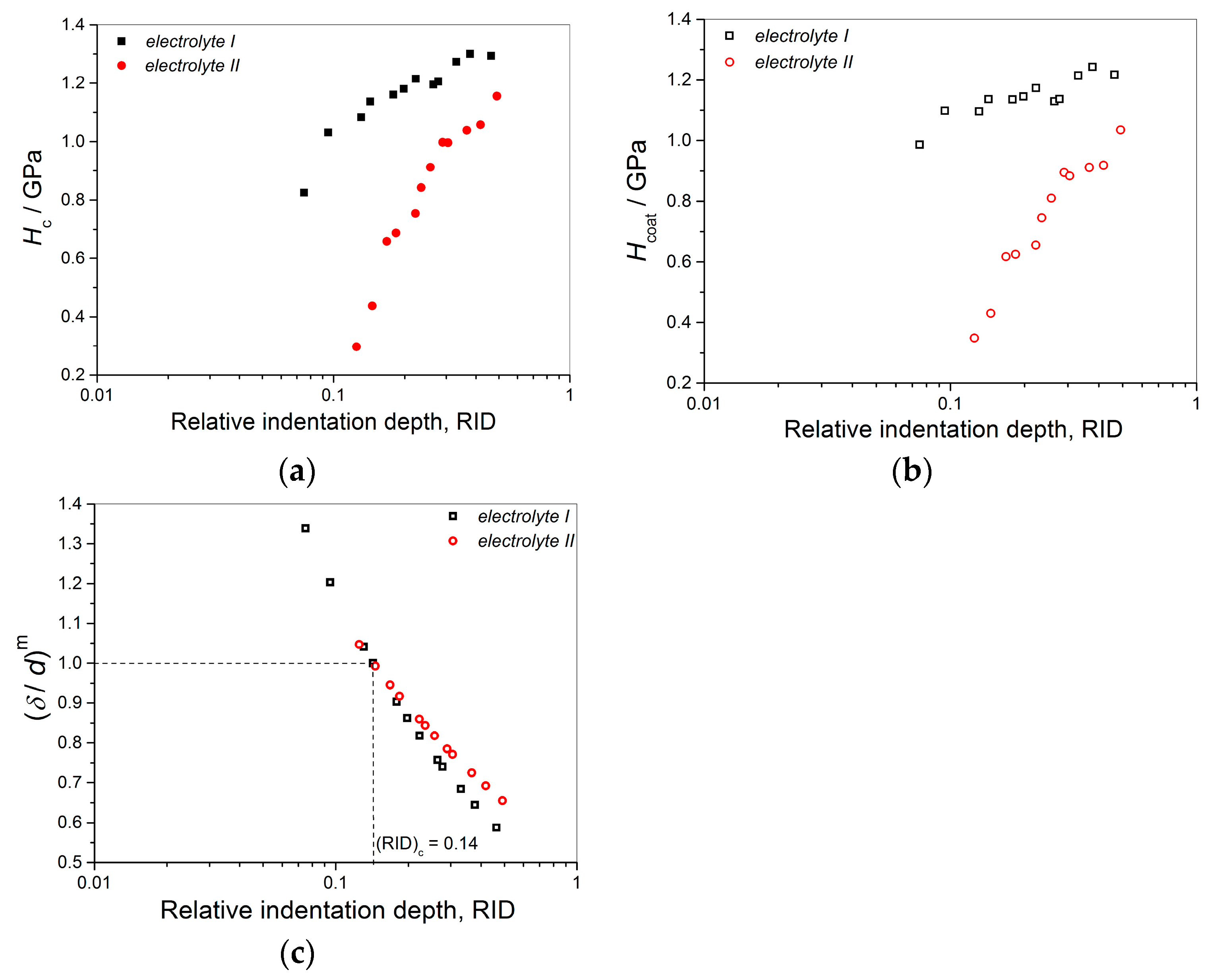
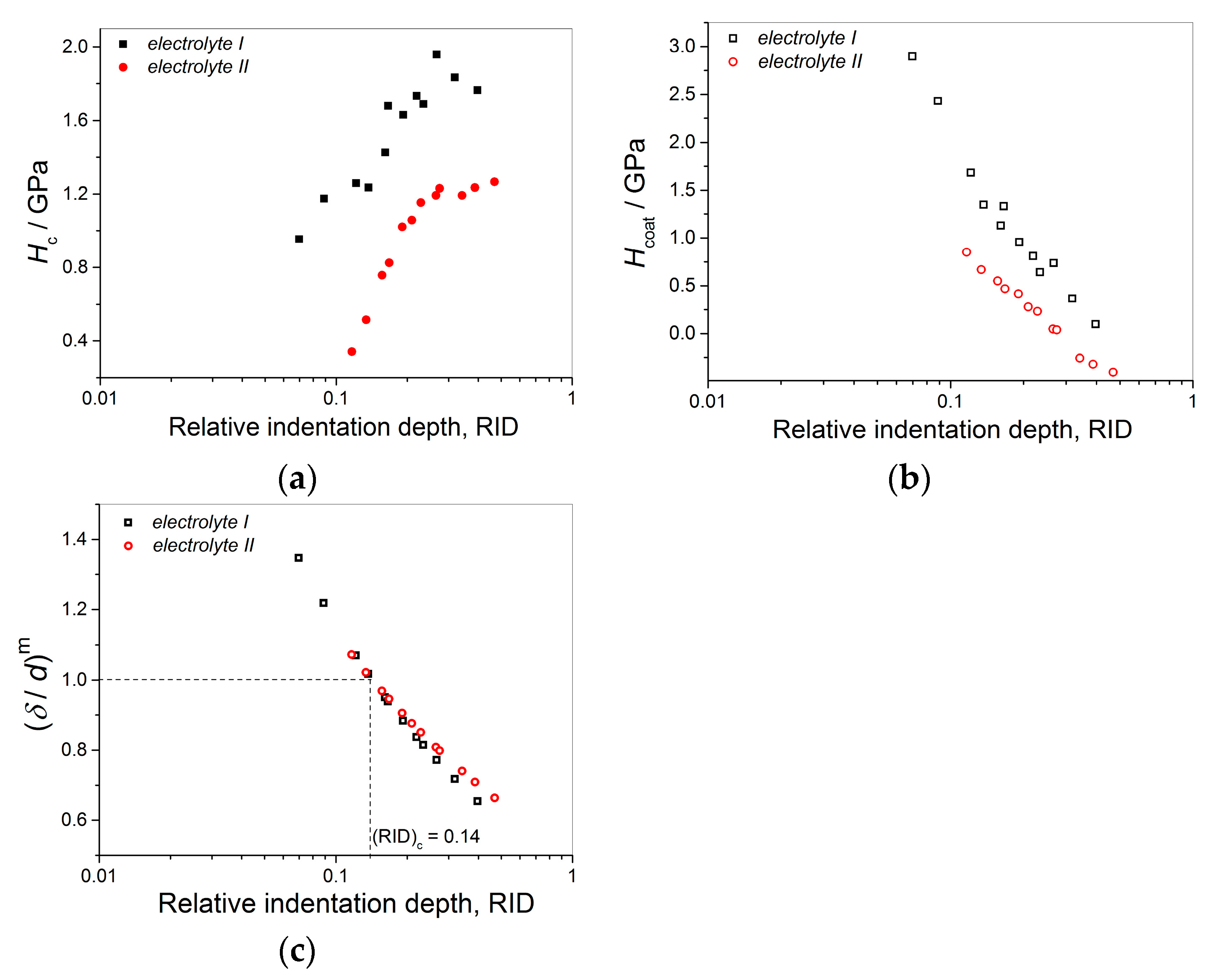
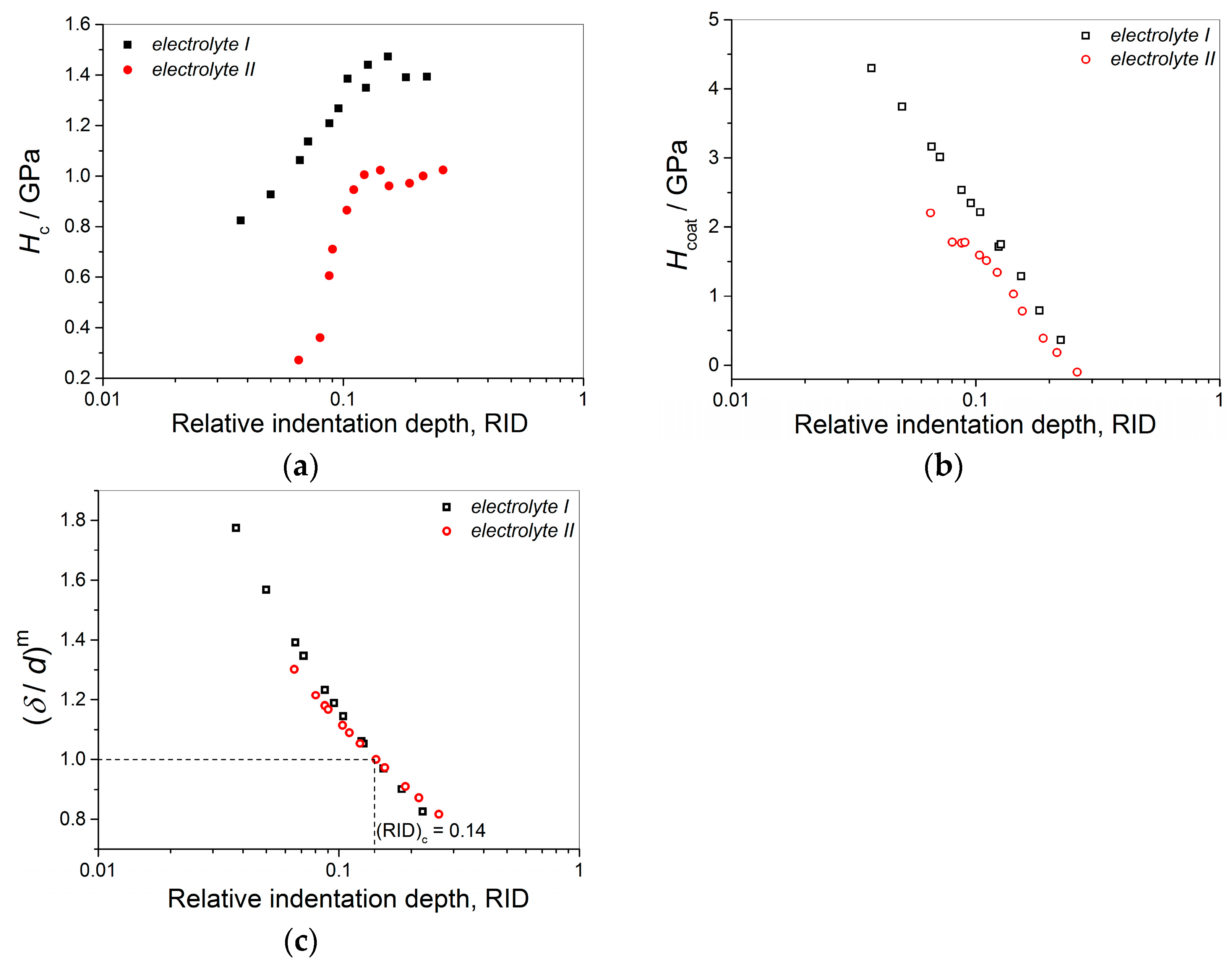
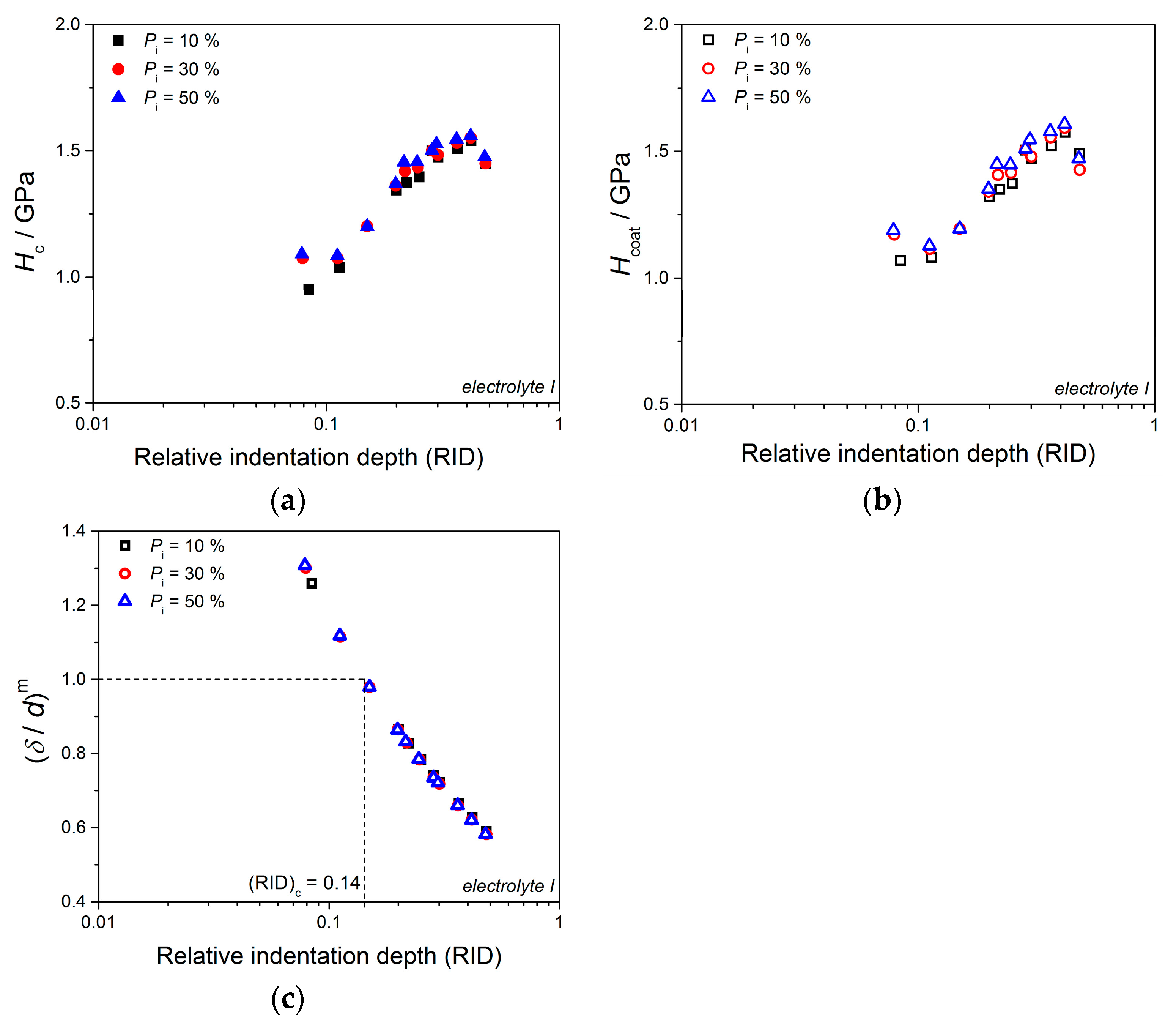
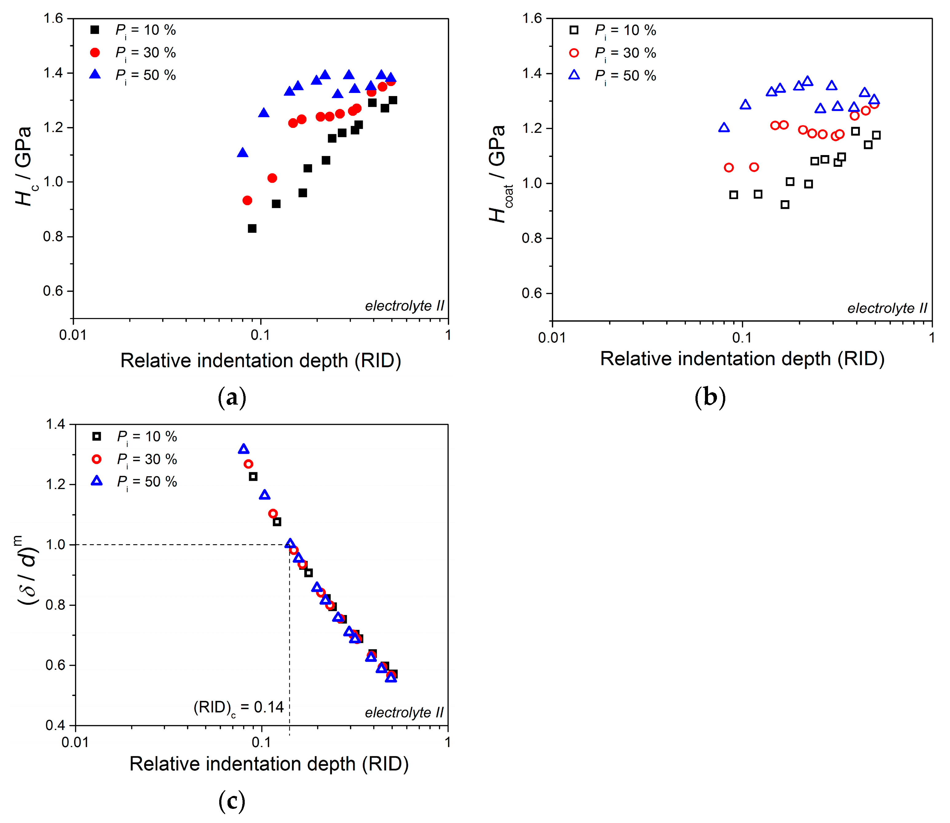
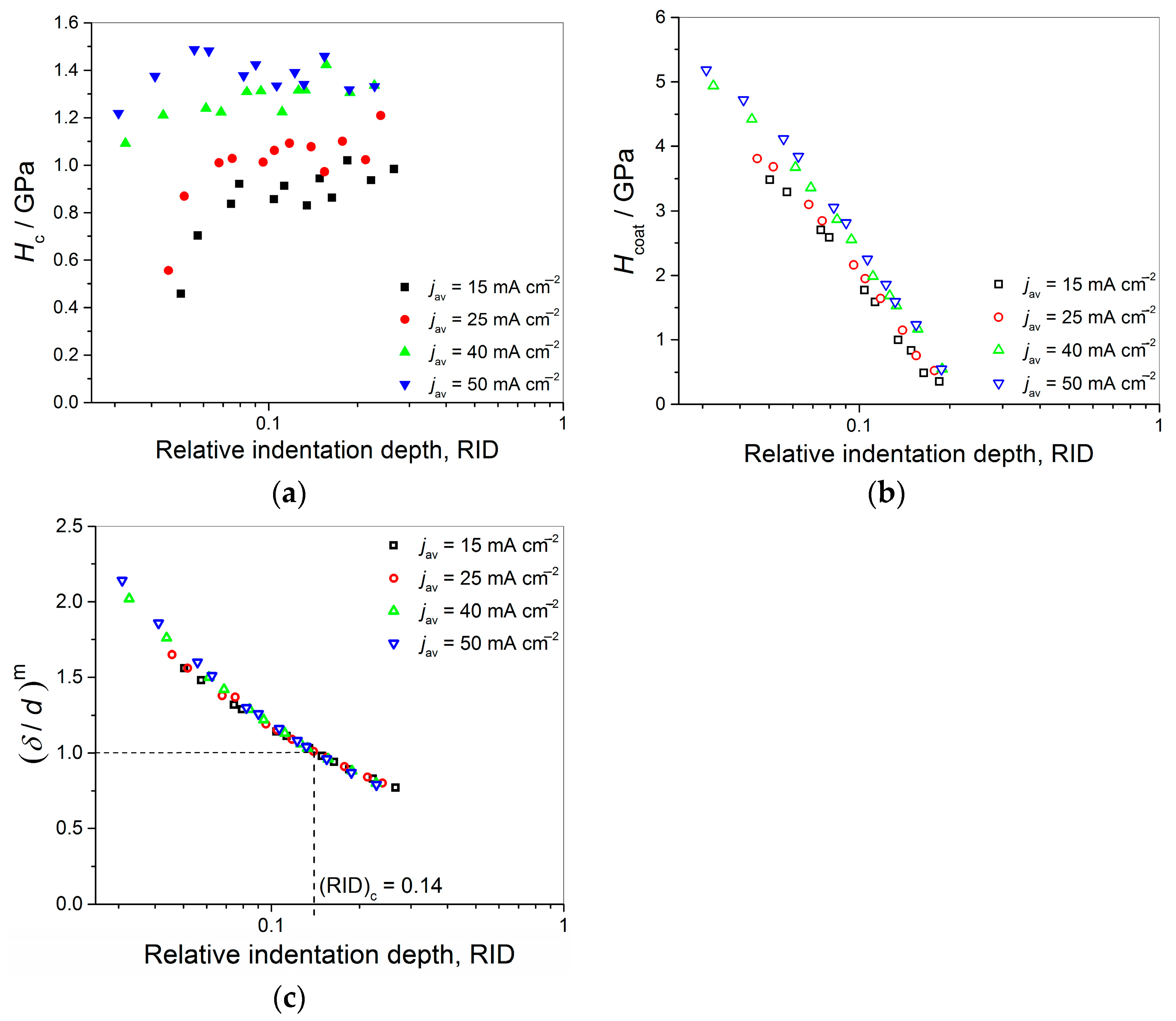
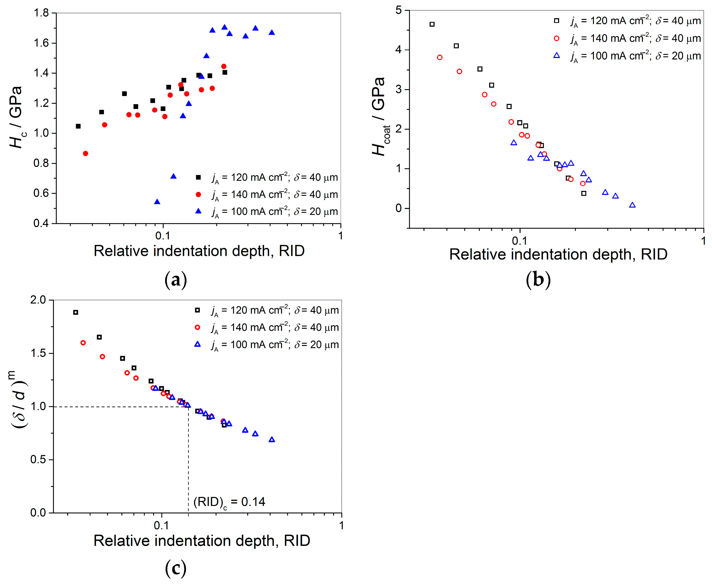
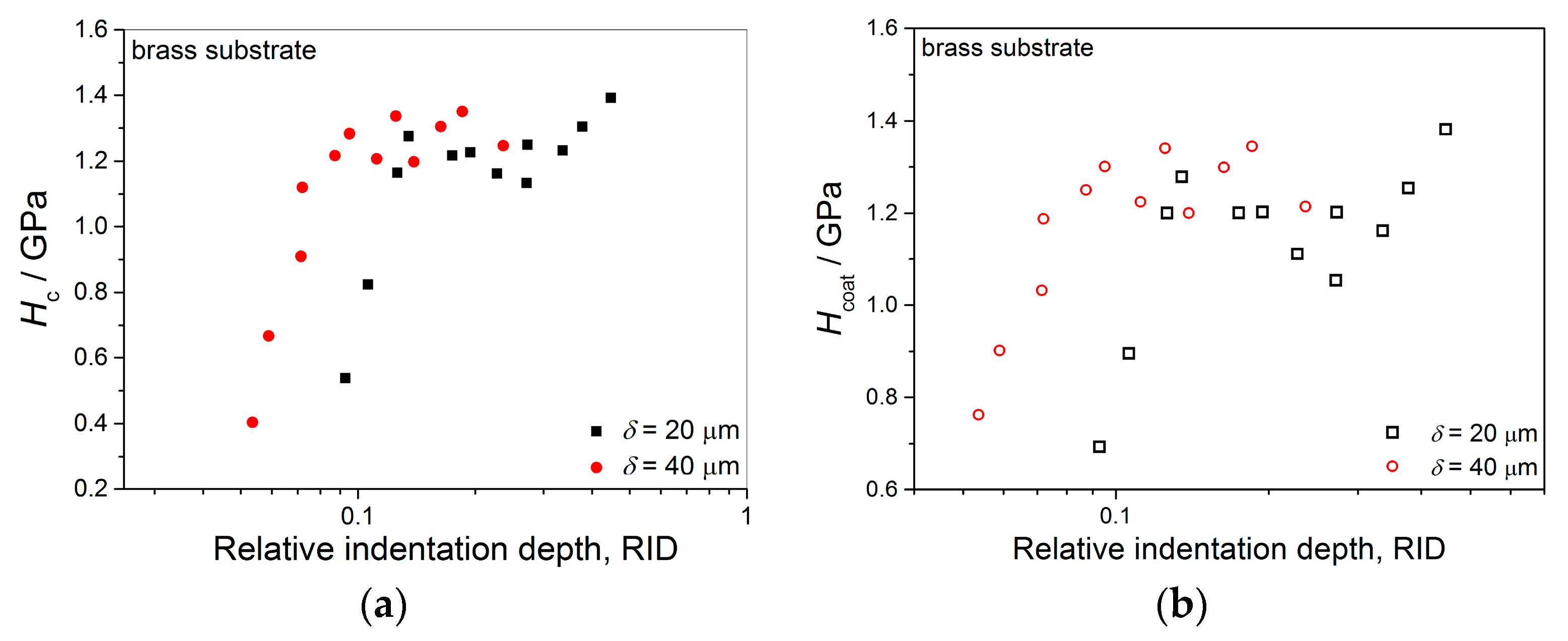
Anyway, the limiting (or critical) RID value of 0.14 [(RID)c = 0.14] showed an universal character for electrolytically produced Cu coatings. This value was observed for both the Cu coatings electrodeposited in the DC regime under various electrodeposition conditions (the types of electrolyte and cathode, coating thickness and electrolyte stirring) and for various PC regimes. This value is related with the coating thickness as (hc/δ) = 0.14, i.e., as hc = 0.14δ. For values of an indentation depth smaller than this critical value, hc, (i.e., for hc < 0.14δ) a substrate (cathode) had not any significant influence on the coating hardness and the measured hardness can be equaled with the coating hardness. For hc ≥ 0.14δ, the cathode hardness strongly contributes to the measured composite hardness, and it is necessary to apply the C–L model to obtain an absolute hardness of the Cu coatings. This criteria (hc = 0.14δ) is situated between the value hc < 0.20δ [70] established for polycrystalline soft coatings on hard substrates. Such as, the Cu coatings produced on Si(111) and brass cathodes, for which a substrate had no influence on the coating hardness, and Buckle’s one-tenth rule predicting that a film thickness of 10 times the indentation depth is sufficient to neglect the influence of the substrate, i.e., a substrate commences to effect on the coating hardness after hc > 0.10δ [51].
The coating hardness values calculated applying the C–L model were in a line with those obtained in other investigations for the Cu coatings obtained by different electrochemical deposition processes. Depending on parameters of the electrodeposition, the values of hardness of Cu coatings electrodeposited by the DC regimes were between 0.70 and 1.65 GPa [61,78,79]. For example, the Cu coating hardness value determined by Korsunsky model was 0.80 GPa [41]. The values of coating hardness for the Cu coatings produced by different periodically changing regimes of the electrochemical deposition were in the 1.10–2.0 GPa range, and they were slightly higher than the values obtained by the DC mode [80].

7. Copper Matrix Composites

In the last decades, an effort in a production of Cu coatings suitable for application in various industries is moved towards an improvement of their mechanical characteristics. It is attained by an incorporation of various particles, known as reinforcements, into the Cu coatings. The particles are suspended into an electrolyte and incorporated (co-deposited) into a Cu coating during electrodeposition process, producing copper matrix composites (CMCs) [81]. All reinforcements can be situated into one of two groups [82]:
I.
Metal ceramics, such as zirconia (ZrO2) [83], Al2O3 [84,85], nitrides (Si3N4) [81,86,87], silicon carbide (SiC) [88,89], silica (SiO2) [90], TiO2 [91,92], etc., and
II.
Carbon nanomaterials, such as carbon nanotube (CNT) [82,93], multi walled carbon nanotube (MWCNT) [94,95], and graphene (Gr) and its derivatives such as (graphene oxides (GO) and reduced graphene oxides (RGO)) [96,97,98,99,100,101,102].
The addition of the first group of the reinforcements to the electrolyte improves a hardness of electrodeposited Cu coatings, but always causes a decrease of the electrical conductivity due to inferior electrical conductivity of metal ceramic particles [82]. On the other hand, carbon nanomaterials possess excellent both electrical and thermal conductivities, making them superior in a production of copper matrix composites relative to those obtained with ceramic reinforcements. The combination of two types of particles, such as Gr and CNT, is often used for a synthesis of Cu matrix composites of enhanced mechanical characteristics [82].
The processes of electrodeposition from electrolytes with suspended particles by which copper matrix composites are produced are known as electrolytic co-deposition or composite plating processes [81]. All parameters and regimes of the electrodeposition reported in Section 2 and Section 4 are also applied for obtaining of Cu matrix composites [81,82,83,84,85,86,87,88,89,90,91,92,93,94,95,96,97,98,99,100,101,102].
Anyway, various research groups reported about an enhanced hardness of Cu coatings electrodeposited with the reinforcements relative to those obtained from reinforcements-free electrolytes [81,83,97]. Also, the existence of optimal concentration of particles such as ZrO2 giving the coatings of maximum hardness is reported [83]. The decrease of the coating hardness after an attained maximum value can be attributed to a process of agglomeration with the high, applied concentration of the particles. The increase in hardness of coatings can be attributed to [97]: (a) particle strengthening—related with the incorporation of hard particles in a coating and a volume fraction above 20%, (b) dispersion strengthening—related with the incorporation of fine particles (<1 µm) and a volume fraction lower than 15%, and (c) grain refining—related with the nucleation of small grains on surface of the incorporated particles, resulting in a general structural refinement. The presence of smaller grains in coating impedes a dislocation motion, resulting in an increase of microhardness.

8. Conclusions

The effect of various parameters and regimes of the electrochemical deposition on morphology, structure and hardness of copper coatings is summarized. The coatings of copper were obtained by galvanostatically varying the following parameters: the kind of solution (the basic sulfate solution and a solution with an added leveling/brightening additives), the kind of cathode (Si(111) and brass), the electrolysis time (or coating thickness) and stirring of the electrolyte (magnetic stirring and stirring by ultrasound). The Cu coatings of different thicknesses were produced from basic sulfate electrolyte on both Si(111) and brass cathodes by pulsating current (PC) regime varying the average current density (or frequency) and the current density amplitude. Morphology and structure of the Cu coatings were characterized by scanning electron microscopy (SEM) and by atomic force microscopy (AFM) techniques and X-ray diffraction (XRD), respectively, and hardness of the Cu coatings was examined by Vickers microindentation. The coatings of Cu on the Si(111) and the brass substrates belong to “soft film on hard substrate” composite hardness system, and the Chicot–Lesage (C–L) composite hardness model was applied to estimate a hardness of the Cu coatings.
On the basis of presented analyses, it follows that application of the C–L model represents valuable way for an estimation of hardness of the copper coatings. Applying this model, it is established the critical (or limiting) relative indentation depth (RID) of 0.14 separating the zone where measured (composite) hardness is equal to hardness of the coating from the zone where it is necessary to apply the C–L model to determine absolute hardness of the Cu coatings. Considering representative parameters in the DC regime and applying the PC regime as type of PRC regimes, it can be concluded that this critical RID value has universal character for the Cu coatings obtained by different electrodeposition regimes.

Author Contributions

Conceptualization, N.D.N.; investigation, I.O.M.; writing—original draft preparation N.D.N.; methodology, N.D.N. and I.O.M.; formal analysis, I.O.M.; writing—review and editing, N.D.N. and I.O.M.; software, I.O.M.; validation, N.D.N. and I.O.M.; visualization, N.D.N. and I.O.M.; supervision, N.D.N.; funding acquisition, N.D.N. All authors have read and agreed to the published version of the manuscript.

Funding

This work was financially supported by Ministry of Science, Technological Development and Innovation of Republic of Serbia (Grant No. 451-03-47/2023-01/200026).

Institutional Review Board Statement

Not applicable.

Informed Consent Statement

Not applicable.

Data Availability Statement

The data presented in this study are available on request from the corresponding author or co-authors. The data are not publicly available.

Acknowledgments

This work was funded by Ministry of Science, Technological Development and Innovation of Republic of Serbia.

Conflicts of Interest

The authors declare no conflict of interest.

References

  1. Copper Plating Service. Available online: https://www.sharrettsplating.com/coatings/copper (accessed on 10 February 2023).
  2. Bharadishettar, N.; Bhat, U.K.; Panemangalore, D.B. Coating technologies for copper based antimicrobial active surfaces: A perspective review. Metals 2021, 11, 711. [Google Scholar] [CrossRef]
  3. Rohan, J.F.; Thompson, D. Frontiers of Cu Electrodeposition and Electroless plating for On-chip Interconnects. In Copper Electrodeposition for Nanofabrication of Electronics Devices; Kondo, K., Alkolkar, R.N., Barkey, D.P., Yokoi, M., Eds.; Springer: New York, NY, USA, 2014; Volume 171, pp. 99–101. [Google Scholar] [CrossRef]
  4. Ranjan, A.; Islam, A.; Pathak, M.; Khan, M.K.; Keshri, A.K. Plasma sprayed copper coatings for improved surface and mechanical properties. Vacuum 2019, 168, 108834. [Google Scholar] [CrossRef]
  5. Della Gatta, R.; Perna, A.S.; Viscusi, A.; Pasquino, G.; Astarita, A. Cold spray deposition of metallic coatings on polymers: A review. J. Mater. Sci. 2022, 57, 27–57. [Google Scholar] [CrossRef]
  6. Perna, A.S.; Astarita, A.; Carlone, P.; Guthmann, X.; Viscusi, A. Characterization of Cold-Spray Coatings on Fiber-Reinforced Polymers through Nanoindentation Tests. Metals 2021, 11, 331. [Google Scholar] [CrossRef]
  7. Wei, C.; Wu, G.; Yang, S.; Liu, Q. Electrochemical deposition of layered copper thin films based on the diffusion limited aggregation. Sci. Rep. 2016, 6, 34779. [Google Scholar] [CrossRef]
  8. Popov, K.I.; Djokić, S.S.; Nikolić, N.D.; Jović, V.D. Morphology of Electrochemically and Chemically Deposited Metals; Springer International Publishing: New York, NY, USA, 2016. [Google Scholar] [CrossRef]
  9. Mechanical Properties of Materials. Available online: https://www.weldingandndt.com/mechanical-properties-of-materials/ (accessed on 31 January 2023).
  10. Nikolić, N.D.; Rakočević, Z.; Popov, K.I. Structural Characteristics of Bright Copper Surfaces. J. Electroanal. Chem. 2001, 514, 56–66. [Google Scholar] [CrossRef]
  11. Nikolić, N.D.; Rakočević, Z.; Popov, K.I. Reflection and structural analyses of mirror bright metal coatings. J. Solid State Electrochem. 2004, 8, 526–531. [Google Scholar] [CrossRef]
  12. Mladenović, I.O.; Lamovec, J.S.; Vasiljević-Radović, D.G.; Vasilić, R.; Radojević, V.J.; Nikolić, N.D. Implementation of the Chicot–Lesage Composite Hardness Model in a Determination of Absolute Hardness of Copper Coatings Obtained by the Electrodeposition Processes. Metals 2021, 11, 1807. [Google Scholar] [CrossRef]
  13. Mladenović, I.O.; Lamovec, J.S.; Vasiljević Radović, D.G.; Vasilić, R.; Radojević, V.J.; Nikolić, N.D. Morphology, Structure and Mechanical Properties of Copper Coatings Electrodeposited by Pulsating Current (PC) Regime on Si(111). Metals 2020, 10, 488. [Google Scholar] [CrossRef]
  14. Avramović, L.; Maksimović, V.M.; Baščarević, Z.; Ignjatović, N.; Bugarin, M.; Marković, R.; Nikolić, N.D. Influence of the Shape of Copper Powder Particles on the Crystal Structure and Some Decisive Characteristics of the Metal Powders. Metals 2019, 9, 56. [Google Scholar] [CrossRef]
  15. Berube, L.P.; Esperance, G.L. A Quantitative Method of Determining of the Degree of Texture of Zinc Electrodeposits. J. Electrochem. Soc. 1989, 136, 2314–2315. [Google Scholar] [CrossRef]
  16. Nikolić, N.D.; Maksimović, V.M.; Avramović, L. Correlation of Morphology and Crystal Structure of Metal Powders Produced by Electrolysis Processes. Metals 2021, 11, 859. [Google Scholar] [CrossRef]
  17. Mladenović, I.O.; Lamovec, J.S.; Jović, V.B.; Obradov, M.; Vasiljević Radović, D.G.; Nikolić, N.D.; Radojević, V.J. Mechanical characterization of copper coatings electrodeposited onto different substrates with and without ultrasound assistance. J. Serb. Chem. Soc. 2019, 84, 729–741. [Google Scholar] [CrossRef]
  18. Mladenović, I.O.; Bošković, M.V.; Vuksanović, M.M.; Nikolić, N.D.; Lamovec, J.S.; Vasiljević Radović, D.G.; Radojević, V.J. Structural, Mechanical and Electrical Characteristics of Copper Coatings Obtained by Various Electrodeposition Processes. Electronics 2022, 11, 443. [Google Scholar] [CrossRef]
  19. Mladenović, I.O.; Lamovec, J.S.; Vasiljević Radović, D.G.; Radojević, V.J.; Nikolić, N.D. Influence of intensity of ultrasound on morphology and hardness of copper coatings obtained by electrodeposition. J. Electrochem. Sci. Eng. 2022, 12, 603–615. [Google Scholar] [CrossRef]
  20. Chen, Q.; Wang, Z.; Cai, J.; Lui, L. The influence of ultrasonic agitation on copper electroplating of blind-vias for SOI three-dimensional integration. Microelectron. Eng. 2010, 87, 527–531. [Google Scholar] [CrossRef]
  21. Wang, Y.-Q.; Fu, X.-L.; Xu, W.-L.; Li, M.; Zhang, X.-X. Effects of Ultrasound on Rate and Characterization of Copper Electrodeposition. Chin. J. Process Eng. 2004, 4, 305–309. [Google Scholar]
  22. Costa, J.M.; Neto, A.F.A. Ultrasound-assisted electrodeposition and synthesis of alloys and composite materials: A review. Ultrason. Sonochem. 2020, 68, 105193. [Google Scholar] [CrossRef]
  23. Lesage, J.; Pertuz, A.; Puchi-Cabrera, E.S.; Chicot, D. A model to determine the surface hardness of thin films from standard micro-indentation tests. Thin Solid Film. 2006, 497, 232–238. [Google Scholar] [CrossRef]
  24. Lamovec, J.; Jović, V.; Ranđelović, D.; Aleksić, R.; Radojević, V. Analysis of the composite and film hardness of electrodeposited nickel coatings on different substrates. Thin Solid Film. 2008, 516, 8646–8654. [Google Scholar] [CrossRef]
  25. Fuguo, L.; Jinghui, L.; Bo, C.; Chengpeng, W.; Lei, W. Size effects at dwell stage of micro-indentation for pure aluminum. Rare Met. Mater. Eng. 2014, 12, 2931–2936. [Google Scholar] [CrossRef]
  26. Hong, S.H.; Kim, K.S.; Kim, Y.M.; Hahn, J.H.; Lee, C.S.; Park, J.H. Characterization of elastic moduli of Cu thin films using nanoindentation technique. Compos. Sci. Technol. 2005, 65, 1401–1408. [Google Scholar] [CrossRef]
  27. Saha, R.; Xue, Z.; Huang, Y.; Nix, W.D. Indentation of a soft metal film on a hard substrate: Strain gradient hardening effects. J. Mech. Phys. Solids 2011, 49, 1997–2014. [Google Scholar] [CrossRef]
  28. Zong, Z.; Lou, J.; Soboyejo, O.O.; Elmustafa, A.A.; Hammada, F.; Soboyejo, W.O. Indentation size effects in the nano- and micro-hardness of fcc single crystal metals. Mater. Sci. Eng. A 2006, 434, 178–187. [Google Scholar] [CrossRef]
  29. Elmustafa, A.A.; Stone, D.S. Indentation size effect in polycrystalline F.C.C. metals. Acta Mater. 2002, 50, 3641–3650. [Google Scholar] [CrossRef]
  30. Beegan, D.; Chowdhury, S.; Laugier, M.T. Modification of composite hardness models to incorporate indentation size effects in thin films. Thin Solid Film. 2008, 516, 3813–3817. [Google Scholar] [CrossRef]
  31. Bull, S.J.; Rickerby, D.S. New developments in the modeling of the hardness and scratch adhesion of thin films. Surf. Coat. Technol. 1990, 42, 149–164. [Google Scholar] [CrossRef]
  32. Burnett, P.J.; Rickerby, D.S. The mechanical properties of wear-resistant coatings. II: Experimental studies and interpretation of hardness. Thin Solid Film. 1987, 148, 51–65. [Google Scholar] [CrossRef]
  33. Lesage, J.; Chicot, D. A model for hardness determination of thin coatings from standard microindentation test. Surf. Coat. Technol. 2005, 200, 886–889. [Google Scholar] [CrossRef]
  34. Chicot, D.; Lesage, J. Absolute hardness of films and coatings. Thin Solid Film. 1995, 254, 123–130. [Google Scholar] [CrossRef]
  35. Korsunsky, A.M.; McGurk, M.R.; Bull, S.J.; Page, T.F. On the hardness of coated systems. Surf. Coat. Technol. 1998, 99, 171–183. [Google Scholar] [CrossRef]
  36. Guštin, A.Z.; Žužek, B.; Podgornik, B. Hardness measurement of thin strips. Measurement 2021, 182, 109633. [Google Scholar] [CrossRef]
  37. Ma, Z.S.; Zhou, Y.C.; Long, S.G.; Lu, C. On the intrinsic hardness of a metallic film/substrate system: Indentation size and substrate effects. Int. J. Plast. 2012, 34, 1–11. [Google Scholar] [CrossRef]
  38. Chen, M.; Gao, J. The adhesion of copper films coated on silicon and glass substrates. Mod. Phys. Lett. B 2000, 14, 103–108. [Google Scholar] [CrossRef]
  39. He, J.L.; Li, W.Z.; Li, H.D. Hardness measurement of thin films: Separation from composite hardness. Appl. Phys. Lett. 1996, 69, 1402. [Google Scholar] [CrossRef]
  40. Hou, Q.; Gao, J.; Li, S. Adhesion and its influence on micro-hardness of DLC and SiC films. Eur. Phys. J. B 1999, 8, 493–496. [Google Scholar] [CrossRef]
  41. Magagnin, L.; Maboudian, R.; Carraro, C. Adhesion evaluation of immersion plating copper films on silicon by microindentation measurements. Thin Solid Film. 2003, 434, 100–105. [Google Scholar] [CrossRef]
  42. Jonsson, B.; Hogmark, S. Hardness Measurements of Thin Films. Thin Solid Film. 1984, 114, 257–269. [Google Scholar] [CrossRef]
  43. Puchi-Cabrera, E.S. A new model for the computation of the composite hardness of coated Systems. Surf. Coat. Technol. 2002, 160, 177–186. [Google Scholar] [CrossRef]
  44. Tricoteaux, A.; Puchi-Cabrera, E.S.; Lesage, J. Method for fast determination of thin films hardness from standard microindentation tests. Surf. Eng. 2007, 23, 40–44. [Google Scholar] [CrossRef]
  45. Mladenović, I.O.; Nikolić, N.D.; Lamovec, J.S.; Vasiljević Radović, D.G.; Radojević, V.J. Application of the Composite Hardness Models in the Analysis of Mechanical Characteristics of Electrolytically Deposited Copper Coatings: The Effect of the Type of Substrate. Metals 2021, 11, 111. [Google Scholar] [CrossRef]
  46. Mladenović, I.O.; Lamovec, J.S.; Vasiljević-Radović, D.G.; Radojević, V.J.; Nikolić, N.D. Mechanical features of copper coatings electrodeposited by the pulsating current (PC) regime on Si(111) substrate. Int. J. Electrochem. Sci. 2020, 15, 12173–12191. [Google Scholar] [CrossRef]
  47. Hirayama, S.; Iwai, H.; Tanimoto, Y. Mechanical Evaluation of Five Flowable Resin Composites by the Dynamic Micro-Indentation Method. J. Dent. Biomech. 2014, 5, 1758736014533983. [Google Scholar] [CrossRef] [PubMed]
  48. Giannakopoulos, A.E.; Larsson, P.-L.; Vestergaard, R. Analysis of Vickers Indentation. Int. J. Solids Struct. 1994, 31, 2679–2708. [Google Scholar] [CrossRef]
  49. Fang, T.-H.; Chang, W.-J. Nanomechanical properties of copper thin films on different substrates using the nanoindentation technique. Microelectron. Eng. 2003, 65, 231–238. [Google Scholar] [CrossRef]
  50. Li, H.; Bradt, R.C. Knoop microhardness anisotropy of single-crystal LaB6. Mater. Sci. Eng. A 1991, 142, 51–61. [Google Scholar] [CrossRef]
  51. Buckle, H. The Science of Hardness Testing and Its Research Applications; Westbrook, J.W., Conrad, H., Eds.; American Society for Metals: Metals Park, OH, USA, 1973; p. 453. [Google Scholar]
  52. Chandrasekar, M.S.; Pushpavanam, M. Pulse and pulse reverse plating—Conceptual, advantages and applications. Electrochim. Acta 2008, 53, 3313–3322. [Google Scholar] [CrossRef]
  53. Popov, K.I.; Maksimović, M.D. Theory of the Effect of Electrodeposition at a Periodically Changing Rate on the Morphology of Metal Deposits. In Modern Aspects of Electrochemistry; Conway, B.E., Bockris, J.O.M., White, R.E., Eds.; Plenum Press: New York, NY, USA, 1989; Volume 19, pp. 193–250. [Google Scholar] [CrossRef]
  54. Mladenović, I.O.; Lamovec, J.S.; Vasiljević-Radović, D.G.; Radojević, V.J.; Nikolić, N.D. Determination of the absolute hardness of electrolytically produced copper coatings by application of the Chicot–Lesage composite hardness model. J. Serb. Chem. Soc. 2022, 87, 899–910. [Google Scholar] [CrossRef]
  55. Shao, W.; Pattanaik, G.; Zangari, G. Influence of Chloride Anions on the Mechanism of Copper Electrodeposition from Acidic Sulfate Electrolytes. J. Electrochem. Soc. 2007, 154, D201–D207. [Google Scholar] [CrossRef]
  56. Kondo, K.; Akolkar, R.N.; Barkey, D.P.; Yokoi, M. Copper Electrodeposition for Nanofabrication of Electronics Devices; Springer: New York, NY, USA, 2014; pp. 36–39 and 47–50. [Google Scholar] [CrossRef]
  57. Kim, J.J.; Kim, S.-K.; Kim, Y.S. Catalytic behavior of 3-mercapto-1-propane sulfonic acid on Cu electrodeposition and its effect on Cu film properties for CMOS device metallization. J. Electroanal. Chem. 2003, 542, 61–66. [Google Scholar] [CrossRef]
  58. Plieth, W. Additives in the electrocrystallization process. Electrochim. Acta 1992, 37, 2115–2121. [Google Scholar] [CrossRef]
  59. Muresan, L.M.; Varvara, S.C. Leveling and Brightening Mechanisms in Metal Electrodeposition. In Metal Electrodeposition; Nunez, M., Ed.; Nova Science Publishers, Inc.: New York, NY, USA, 2005; pp. 1–45. [Google Scholar]
  60. Nikolić, N.D. The effects of a magnetic field on the morphologies of nickel and copper deposits: The concept of “effective overpotential”. J. Serb. Chem. Soc. 2007, 72, 787–797. [Google Scholar] [CrossRef]
  61. Martins, L.; Martins, J.; Romeira, A.; Costa, M.E.V.; Costa, J.S.; Bazzaoui, M. Morphology of copper coatings electroplated in an ultrasonic field. Mater. Sci. Forum 2004, 455–456, 844–848. [Google Scholar] [CrossRef]
  62. Nikolić, N.D.; Popov, K.I.; Pavlović, L.J.; Pavlović, M.G. The effect of hydrogen codeposition on the morphology of copper electrodeposits. I. The concept of effective overpotential. J. Electroanal. Chem. 2006, 588, 88–98. [Google Scholar] [CrossRef]
  63. Bockris, J.O.M.; Reddy, A.K.N.; Gamboa-Aldeco, M.E. Modern Electrochemistry 2A. In Fundamentals of Electrodics; Kluwer Academic/Plenum Publishers: Boston, MA, USA, 2000; p. 1333. [Google Scholar] [CrossRef]
  64. Zhang, J.M.; Ma, F.; Xu, K.W. Calculation of the surface energy of FCC metals with modified embedded-atom method. Appl. Surf. Sci. 2004, 229, 34–42. [Google Scholar] [CrossRef]
  65. Wang, S.G.; Tian, E.K.; Lung, C.W. Surface energy of arbitrary crystal plane of bcc and fcc metals. J. Phys. Chem. Solids 2000, 61, 1295–1300. [Google Scholar] [CrossRef]
  66. Nikolić, N.D.; Maksimović, V.M.; Branković, G. Morphological and crystallographic characteristics of electrodeposited lead from the concentrated electrolyte. RSC Adv. 2013, 3, 7466–7471. [Google Scholar] [CrossRef]
  67. Varea, A.; Pellicer, E.; Pané, S.; Nelson, B.J.; Suriñach, S.; Baró, M.D.; Sort, J. Mechanical Properties and Corrosion Behaviour of Nanostructured Cu-rich CuNi Electrodeposited Films. Int. J. Electrochem. Sci. 2012, 7, 1288–1302. [Google Scholar]
  68. Petch, N.J. The cleavage strength of polycrystals. J. Iron Steel Inst. 1953, 174, 25–28. [Google Scholar]
  69. Mishra, R.; Basu, B.; Balasubramaniam, R. Effect of grain size on the tribological behavior of nanocrystalline nickel. Mater. Sci. Eng. A 2004, 373, 370–373. [Google Scholar] [CrossRef]
  70. Manika, I.; Maniks, J. Effect of substrate hardness and film structure on indentation depth criteria for film hardness testing. J. Phys. D Appl. Phys. 2008, 41, 074010. [Google Scholar] [CrossRef]
  71. Manika, I.; Maniks, J. Characteristics of deformation localization and limits to the microhardness testing of amorphous and polycrystalline coatings. Thin Solid Film. 1992, 208, 223–227. [Google Scholar] [CrossRef]
  72. Lebouvier, D.; Gilormini, P.; Felder, E. A kinematic model for plastic indentation of a bilayer. Thin Solid Film. 1989, 172, 227–239. [Google Scholar] [CrossRef]
  73. Bull, S.J. Nanoindentation of coatings. J. Phys. D Appl. Phys. 2005, 38, R393. [Google Scholar] [CrossRef]
  74. Kramer, D.E.; Volinsky, A.A.; Moody, N.R.; Gerberich, W.W. Substrate effects on indentation plastic zone development in thin soft films. J. Mater. Res. 2001, 16, 3150–3157. [Google Scholar] [CrossRef]
  75. Beegan, D.; Chowdhury, S.; Laugier, M.T. The nanoindentation behaviour of hard and soft films on silicon substrates. Thin Solid Film. 2004, 466, 167–174. [Google Scholar] [CrossRef]
  76. Wu, T.W.; Moshref, M.; Alexopoulos, P.S. The effect of the interfacial strength on the mechanical properties of aluminum films. Thin Solid Film. 1990, 187, 295–307. [Google Scholar] [CrossRef]
  77. Pan, H.; He, Y.; Zhang, X. Interactions between Dislocations and Boundaries during Deformation. Materials 2021, 14, 1012. [Google Scholar] [CrossRef]
  78. Kasach, A.A.; Kurilo, I.I.; Kharitonov, D.S.; Radchenko, S.L.; Zharskii, I.M. Sonochemical Electrodeposition of Copper Coatings. Russ. J. Appl. Chem. 2018, 91, 207–213. [Google Scholar] [CrossRef]
  79. Tao, S.; Li, D.Y. Trbological, mechanical and electrochemical properties of nanocrystalline copper deposits produced by pulse electrodeposition. Nanotechnology 2006, 17, 65–78. [Google Scholar] [CrossRef]
  80. Kristof, P.; Pritzker, M. Improved Copper Plating through the Use of Current Pulsing & Ultrasonic Agitation. Plat. Surf. Finish. 1999, 237–240. Available online: http://www.nmfrc.org/pdf/9811237.pdf (accessed on 10 February 2023).
  81. Eslami, M.; Saghafian, H.; Golestani-fard, F.; Robin, A. Effect of electrodeposition conditions on the properties of Cu–Si3N4 composite coatings. Appl. Surf. Sci. 2014, 300, 129–140. [Google Scholar] [CrossRef]
  82. Song, G.; Sun, L.; Li, S.; Sun, Y.; Fu, O.; Pan, C. Synergistic effect of Gr and CNTs on preparing ultrathin Cu-(CNTs+Gr) composite foil via electrodeposition. Compos. B Eng. 2020, 187, 107841. [Google Scholar] [CrossRef]
  83. Akhtar, K.; Hira, U.; Khalid, H.; Zubair, N. Uniform fine particles of ZrO2 as reinforcement filler in the electrodeposited Cu-ZrO2 nanocomposite coating on steel substrate. J. Alloys Compd. 2019, 772, 15–24. [Google Scholar] [CrossRef]
  84. Hayashi, H.; Izumi, S.; Tari, I. Codeposition of α-Alumina Particles from Acid Copper Sulfate Bath. J. Electrochem. Soc. 1993, 140, 362–365. [Google Scholar] [CrossRef]
  85. Gupta, S.K.; Misra, R.D. Experimental study of pool boiling heat transfer on copper surfaces with Cu-Al2O3 nanocomposite coatings. Int. Commun. Heat Mass Transf. 2018, 97, 47–55. [Google Scholar] [CrossRef]
  86. Robin, A.; Santana, J.C.P.d.; Sartori, A.F. Characterization of copper–silicon nitride composite electrocoatings. J. Appl. Electrochem. 2010, 40, 507–513. [Google Scholar] [CrossRef]
  87. Robin, A.; Santana, J.C.P.d.; Sartori, A.F. Co-electrodeposition and characterization of Cu–Si3N4 composite coatings. Surf. Coat. Technol. 2011, 205, 4596–4601. [Google Scholar] [CrossRef]
  88. Zhu, J.; Liu, L.; Zhao, H.; Shen, B.; Hu, W. Microstructure and performance of electroformed Cu/nano-SiC composite. Mater. Des. 2007, 28, 1958–1962. [Google Scholar] [CrossRef]
  89. Banthia, S.; Sengupta, S.; Das, S.; Das, K. Cu, Cu-SiC functionally graded coating for protection against corrosion and wear. Surf. Coat. Technol. 2019, 374, 833–844. [Google Scholar] [CrossRef]
  90. Bengoa, L.N.; Ispas, A.; Bengoa, J.F.; Bund, A.; Egli, W.A. Ultrasound Assisted Electrodeposition of Cu-SiO2 Composite Coatings: Effect of Particle Surface Chemistry. J. Electrochem. Soc. 2019, 166, D244–D251. [Google Scholar] [CrossRef]
  91. Gupta, S.K.; Misra, R.D. An experimental investigation on flow boiling heat transfer enhancement using Cu-TiO2 nanocomposite coating on copper substrate. Exp. Therm. Fluid Sci. 2018, 98, 406–419. [Google Scholar] [CrossRef]
  92. Gupta, S.K.; Misra, R.D. Effect of two-step electrodeposited Cu–TiO2 nanocomposite coating on pool boiling heat transfer performance. J. Therm. Anal. Calorim. 2019, 136, 1781–1793. [Google Scholar] [CrossRef]
  93. Wang, C.; Gan, X.; Tao, J.; Xie, M.; Yi, J.; Liu, Y. Compression and electromagnetic shielding properties of CNTs reinforced copper foams prepared through electrodeposition. Vacuum 2019, 167, 159–162. [Google Scholar] [CrossRef]
  94. Bengoa, L.N.; Seré, P.R.; Pary, P.; Conconi, M.S.; Folgueiras, J.M.; Morel, E.N.; Torga, J.; Egli, W.A. Self-lubricating Cu-MWCNT coatings deposited from an ecofriendly glutamate-based electrolyte. Surf. Coat. Technol. 2020, 388, 125590. [Google Scholar] [CrossRef]
  95. Chakraborty, R.; Sengupta, S.; Das, S.; Saha, P.; Das, K. Synthesis and characterization of MWCNT reinforced nano-crystalline copper coating from a highly basic bath through pulsed electrodeposition. Surf. Interfaces. 2017, 9, 28–35. [Google Scholar] [CrossRef]
  96. Qu, W.; Zhang, J.; Zhang, S.; Li, N.; Liu, C.; Yu, X.; Song, Y.; Han, S.; Chen, L.; Xi, M.; et al. Copper matrix composites reinforced by three-dimensional netlike graphene towards enhanced mechanical property and wear resistance. Compos. Commun. 2022, 32, 101187. [Google Scholar] [CrossRef]
  97. Hidalgo-Manrique, P.; Lei, X.; Xu, R.; Zhou, M.; Kinloch, I.A.; Young, R.J. Copper/graphene composites: A review. J. Mater. Sci. 2019, 54, 12236–12289. [Google Scholar] [CrossRef]
  98. Joseph, A.; Kirubasankar, B.; Mathew, A.M.; Narayanasamy, M.; Yan, C.; Angaiah, S. Influence of pulse reverse current parameters on electrodeposition of copper-graphene nanocomposite coating. Appl. Surf. Sci. Adv. 2021, 5, 100116. [Google Scholar] [CrossRef]
  99. Biswal, H.J.; Vundavilli, P.R.; Gupta, A. Perspective—Electrodeposition of Graphene Reinforced Metal Matrix Composites for Enhanced Mechanical and Physical Properties: A Review. J. Electrochem. Soc. 2020, 167, 146501. [Google Scholar] [CrossRef]
  100. Mathew, R.T.; Singam, S.; Kollu, P.; Bohm, S.; Prasad, M.J.N.V. Achieving exceptional tensile strength in electrodeposited copper through grain refinement and reinforcement effect by co-deposition of few layered graphene. J. Alloys Compd. 2020, 840, 155725. [Google Scholar] [CrossRef]
  101. Yu, J.; Wang, L.; Liu, Z.; Xu, J.; Zong, Y. Electrodeposition-based fabrication of graphene/copper composites with excellent overall properties. J. Alloys Compd. 2022, 924, 166610. [Google Scholar] [CrossRef]
  102. Wang, T.; Zhao, R.; Zhan, K.; Bao, L.; Zhang, Y.; Yang, Z.; Yan, Y.; Zhao, B.; Yang, J. Preparation of electro-reduced graphene oxide/copper composite foils with simultaneously enhanced thermal and mechanical properties by DC electro-deposition method. Mater. Sci. Eng. A 2021, 805, 140574. [Google Scholar] [CrossRef]
Figure 1. The SEM micrographs of the morphology of Cu coatings electrodeposited at a current density of 50 mA cm−2 on the brass cathode from: (a) electrolyte I, and (b) electrolyte II. The thickness of the coatings: 20 μm; The electrolyte stirring: Magnetic stirring (MS); Temperature: 22.0 ± 0.50 °C. Magnification: ×1500 [12].
Metals 13 00683 g001
Figure 2. The 3D (three dimensional) AFM images and the corresponding histograms of the Cu coatings produced from: (a,b) electrolyte I, and (c,d) electrolyte II. The thickness of the coatings: 20 μm. The current density: j = 50 mA cm−2; The cathode: brass; The electrolyte stirring: Magnetic stirring (MS); Temperature: 22.0 ± 0.50 °C. Scan size: (70 × 70) μm2 [12].
Metals 13 00683 g002
Figure 3. The 3D (three dimensional) AFM images and the corresponding histograms of the Cu coatings electrodeposited from: (a,b) electrolyte I, and (c,d) electrolyte II. The thickness of the coatings: 20 μm. The current density: j = 50 mA cm−2; The cathode: Si(111); The electrolyte stirring: Magnetic stirring (MS); Temperature: 22.0 ± 0.50 °C. Scan size: (70 × 70) μm2 [12].
Metals 13 00683 g003
Figure 4. The 3D (three dimensional) AFM images and the corresponding histograms of the Cu coatings electrodeposited from: (a,b) electrolyte I, and (c,d) electrolyte II. The thickness of the coatings: 40 μm. The current density: j = 50 mA cm−2; The cathode: Si(111); The electrolyte stirring: Magnetic stirring (MS); Temperature: 22.0 ± 0.50 °C. Scan size: (70 × 70) μm2 [12].
Metals 13 00683 g004aMetals 13 00683 g004b
Figure 5. The diffractograms of the Cu coatings thicknesses of 40 μm produced by electrodeposition from electrolytes I and II, and Cu standard (04-0836) [12].
Metals 13 00683 g005
Figure 6. The SEM micrographs of the morphology of Cu coatings obtained by electrodeposition at the low temperature (T = 7.0 ± 1.0 °C) at a current density of 50 mA cm−2 on the brass cathodes from electrolyte I with an intensity of ultrasound corresponding to: (a) Pi = 10%, and (b) Pi = 50%. The coating thickness: 16.6 μm [19].
Metals 13 00683 g006
Figure 7. The 3D AFM images and the corresponding histograms of Cu coatings electrodeposited at the low temperature (T = 7.0 ± 1.0 °C) at a current density of 50 mA cm−2 on the brass cathodes from electrolyte I with an intensity of ultrasound corresponding to: (a,b) Pi = 10%, (c,d) Pi = 30%, and (e,f) Pi = 50%. The coating thickness: 16.6 μm. Scan size: (20 × 20) μm2 [19].
Metals 13 00683 g007aMetals 13 00683 g007b
Figure 8. The SEM micrographs of the morphology of Cu coatings electrodeposited at the low temperature (T = 7.0 ± 1.0 °C) at a current density of 50 mA cm−2 on the brass cathodes from electrolyte II with an intensity of ultrasound corresponding to: (a) Pi = 10%, and (b) Pi = 50%. The coating thickness: 16.6 μm [19].
Metals 13 00683 g008
Figure 9. The 3D AFM images and the corresponding histograms of Cu coatings electrodeposited at the low temperature (T = 7.0 ± 1.0 °C) at a current density of 50 mA cm−2 on the brass cathodes from electrolyte II with an intensity of ultrasound corresponding to: (a,b) Pi = 10%, (c,d) Pi = 30%, and (e,f) Pi = 50%. The coating thickness: 16.6 μm. Scan size: (20 × 20) μm2 [19].
Metals 13 00683 g009
Figure 10. The imprint obtained by Vickers microindentation in the electrolytically produced Cu coating. The applied load: 0.49 N. The dwell time: 15 s [46].
Metals 13 00683 g010
Figure 11. The dependencies of: (a) Hc, (b) Hcoat, and (c) parameter (δ/d)m on RID for the 20 μm thick Cu coatings produced at a current density of 50 mA cm−2 on the brass from electrolyte I and electrolyte II [12].
Metals 13 00683 g011
Figure 12. The dependencies of: (a) Hc, (b) Hcoat, and (c) parameter (δ/d)m on RID for the 20 µm thick Cu coatings produced at a current density of 50 mA cm−2 on the Si(111) substrate from electrolyte I and electrolyte II [12].
Metals 13 00683 g012
Figure 13. The dependencies of: (a) Hc, (b) Hcoat, and (c) parameter (δ/d)m on RID for the 40 µm thick Cu coatings electrodeposited at a current density of 50 mA cm−2 on the Si(111) substrate from electrolyte I and electrolyte II [12].
Metals 13 00683 g013
Figure 14. The dependencies of: (a) Hc, (b) Hcoat, and (c) parameter (δ/d)m on RID for the Cu coatings produced from electrolyte I on the brass with various intensities of imposed ultrasound [19].
Metals 13 00683 g014
Figure 15. The dependencies of: (a) Hc, (b) Hcoat, and (c) parameter (δ/d)m on RID for the Cu coatings produced from electrolyte II on the brass with various intensities of imposed ultrasound [19].
Metals 13 00683 g015
Figure 16. The SEM micrographs of morphology of Cu coatings electrodeposited by the PC regime at jav of: (a,b) 15, (c,d) 25, (e,f) 40 and (g,h) 50 mA cm−2. The current density amplitude: jA = 100 mA cm−2; The cathode: Si(111); the coating thickness, δ = 40 μm; Magnification: (a,c,e,g) ×1000, and (b,d,f,h) ×3000 [13].
Metals 13 00683 g016
Figure 17. The 3D AFM images and the histograms of Cu coatings electrodeposited by the PC regime: (a,b) jav = 15 mA cm−2; ν = 30 Hz, (c,d) jav = 25 mA cm−2; ν = 50 Hz, (e,f) jav = 40 mA cm−2; ν = 80 Hz, and (g,h) jav = 50 mA cm−2; ν = 100 Hz. The cathode: Si(111); the coating thickness, δ = 40 μm. Scan size: (70 × 70) μm2 [13].
Metals 13 00683 g017aMetals 13 00683 g017b
Figure 18. The XRD patterns recorded for the Cu coatings produced by the PC regime at various frequencies (or the average current densities), and Cu standard (04-0836) [13].
Metals 13 00683 g018
Figure 19. The SEM micrographs of morphology of Cu coatings electrodeposited by the PC regime with jA of: (a,b) 120, and (c,d) 140 mA cm−2. The cathode: Si(111); the coating thickness, δ = 40 µm; Magnification: (a,c) ×1000, and (b,d) ×3000 [13].
Metals 13 00683 g019
Figure 20. The 3D AFM images and the histograms of Cu coatings electrodeposited by the PC regime: (a,b) jA = 120 mA cm–2, and (c,d) jA = 140 mA cm–2. The cathode: Si(111); the coating thickness, δ = 40 µm. Scan size: (70 × 70) μm2 [13].
Metals 13 00683 g020aMetals 13 00683 g020b
Figure 21. The XRD patterns recorded for the Cu coatings produced by the pulsating current regime with different current density amplitudes, and Cu standard (04-0836) [13].
Metals 13 00683 g021
Figure 22. The 3D AFM image and the histogram of 20 µm thick Cu coating electrodeposited by the pulsating current regime at jav of 50 mA cm−2; jA = 100 mA cm−2; tc = tp = 5 ms: (a) topography, and (b) histogram. The cathode: Si(111). Scan size: (70 × 70) μm2 [13].
Metals 13 00683 g022
Figure 23. The SEM micrographs of the morphology of Cu coatings electrodeposited by the PC regime at jav of 50 mA cm−2. The current density amplitude: jA = 100 mA cm−2; tc = tp = 5 ms; The cathode: brass; the coating thickness, δ = 40 µm; Magnification: (a) ×1000, and (b) ×3000 [45].
Metals 13 00683 g023
Figure 24. The 3D AFM images and the corresponding histograms of the Cu coatings electrodeposited by the PC regime on the brass cathode at jav of 50 mA cm−2: (a,b) 20 µm, and (c,d) 40 µm. jA = 100 mA cm−2; tc = tp = 5 ms. Scan size: (70 × 70) μm2 [45].
Metals 13 00683 g024
Figure 25. The dependencies of: (a) Hc, (b) Hcoat, and (c) parameter (δ/d)m on RID for the Cu coatings produced by the PC regime from electrolyte I on Si(111) substrate at frequencies of 30, 50, 80 and 100 Hz (i.e., at average current densities of 15, 25, 40 and 50 mA cm−2) [13,54].
Metals 13 00683 g025
Figure 26. The dependencies of: (a) Hc, (b) Hcoat, and (c) parameter (δ/d)m on RID for the 40 µm thick Cu coatings produced by the PC regime from electrolyte I on Si(111) substrate at jav (jA) of 60 and 70 mA cm−2 (120 and 140 mA cm−2, respectively), and 20 µm thick Cu coating electrodeposited under the same conditions at jav (jA) of 50 mA cm−2 (100 mA cm−2) [13,54].
Metals 13 00683 g026
Figure 27. The dependencies of: (a) Hc, (b) Hcoat, and (c) parameter (δ/d)m on RID for 20 and 40 µm thick Cu coatings produced by the pulsating current regime from electrolyte I on the brass cathode at jav (jA) of 50 mA cm−2 (100 mA cm−2) [45].
Metals 13 00683 g027aMetals 13 00683 g027b
Figure 28. The deformation of the Cu coatings around an indenter as a function of the applied load: (a) the Cu coating produced from electrolyte I in the DC mode at j = 33 mA cm−2, (P = 4.903 N, d = 84.4 μm), and (b) the Cu coating produced from electrolyte II in the DC mode at j = 67 mA cm−2 with ultrasound assistance (P = 0.981 N, d = 39.6 μm) [18].
Metals 13 00683 g028
Table 1. The values of TC and RTC coefficients calculated for the Cu coatings electrodeposited from electrolyte I and electrolyte II; (electrolyte I—I; electrolyte II—II; s—Cu standard). R is an intensity of the diffraction peak [12].
PlaneR (in%)RsTCRTC (in%)
(hkl)RIRII(in%)TCITCIIRTCIRTCII
(111)7.93.3154.60.1450.0611.711.47
(200)3.292.1225.10.1273.671.4988.31
(220)84.04.0510.97.710.3790.678.90
(311)4.90.529.40.5210.0556.131.32
Table 2. The values of Meyer’s index (m) for the Cu coatings electrodeposited with different intensities of ultrasound [19].
Pi/%103050
m (electrolyte I)0.45030.45940.4750
m (electrolyte II)0.44070.45650.4725
Table 3. The parameters of the pulsating current (PC) regime used in the electrodeposition processes. jA—the current density amplitude, tc—deposition time (on period), tp—pause time (off period), p—the pause-to-pulse ratio, jav—the average current density and ν—frequency [13].
Number of SamplesjA/mA cm−2tc/mstp/msδ/µmjav/mA cm−2ν/Hz
1100554050100
210057.5404080
3100515402550
4100528.3401530
5120554060100
6140554070100
7100552050100
Table 4. The Ra values of roughness obtained for the Cu coatings produced at different average current densities (or frequencies) [13].
jav/mA cm−215254050
Ra / nm507.3 ± 3.2470.5 ± 2.9385 ± 2.4169.9 ± 2.1
Table 5. TC and RTC coefficients calculated for Cu coatings produced by the PC regimes at frequencies of 30 and 50 Hz; s—Cu standard; R is an intensity of diffraction peak [13].
PlaneR (in%)RsTCRTC (in%)
(hkl)R30 HzR50 Hz(in%)TC30 HzTC50 HzRTC30 HzRTC50 Hz
(111)4.058.654.60.0731.070.8822.8
(200)11.26.925.10.450.275.45.8
(220)81.922.210.97.52.049043.5
(311)2.912.39.40.311.313.7227.9
Table 6. TC and RTC coefficients calculated for Cu coatings produced by the PC regimes at frequencies of 80 and 100 Hz; s—Cu standard; R is an intensity of diffraction peak [13].
PlaneR (in%)RsTCRTC (in%)
(hkl)R80 HzR100 Hz(in%)TC80 HzTC100 HzRTC80 HzRTC100 Hz
(111)67.372.754.61.231.3328.235.9
(200)5.07.125.10.200.284.67.6
(220)3.64.010.90.330.377.610
(311)24.116.29.42.61.7259.646.5
Table 7. Texture calculations for the Cu coatings obtained by the PC regimes with jA of 120 and 140 mA cm−2; s—Cu standard; R is an intensity of diffraction peak [13].
Plane (hkl)R (in%)RsTCRTC (in%)
R120R140(in%)TC120TC140RTC120RTC140
(111)86.195.854.61.581.7554.383.3
(200)2.01.2625.10.0800.0502.72.4
(220)1.30.7610.90.120.0704.13.3
(311)10.62.189.41.130.2338.911.0
Table 8. The Meyer’s index, m values for the Cu coatings electrodeposited by different PC regimes [13,54].
jav/mA cm−2152540506070
m0.42880.43720.47700.49790.43460.3447
Disclaimer/Publisher’s Note: The statements, opinions and data contained in all publications are solely those of the individual author(s) and contributor(s) and not of MDPI and/or the editor(s). MDPI and/or the editor(s) disclaim responsibility for any injury to people or property resulting from any ideas, methods, instructions or products referred to in the content.

