1. Introduction
With the advancement in power electronics technology, induction heating (IH) appliances have proved to be a better replacement for conventional electrical and gas heating technologies [
1]. They are widely used in many domestic and industrial applications, with inherent advantages over their classical counterparts, such as resistive heating, flame heating, or arc furnaces. They offer a higher conversion efficiency and a notably lower time constant in attaining heat [
2].
The IH system has a high-frequency alternating current which is fed to a work coil for the generation of a high-frequency alternating magnetic field. The latter cuts the material to be heated, which is commonly known as a work-piece. The heating takes place because of two diversified phenomena, namely eddy loss and hysteresis loss [
3]. The former takes place due to Joule’s law of heating, while the latter takes place due to the continuous magnetization and demagnetization of the ferromagnetic material-based work-piece. The hysteresis loss is directly proportional to the operating frequency, while the eddy current loss is directly proportional to the square of the operating frequency [
4]. Thus, the aforementioned losses and, in turn, the magnitude of the heat generated, depend upon the operating frequency. The latter generally lies in the range between 15 kHz and 70 kHz for domestic and industrial applications, while it goes up to a few MHz for medical applications [
5]. The high switching frequency in IH applications offers some more advantages, such as a reduction in the size of the magnetic components and a higher flux density around the workpiece. Therefore, there is a considerable reduction in the size of the converter at the same power rating [
6].
However, the high-frequency operation of non-linear switching electronic devices generates a considerable amount of high-frequency harmonics. The latter has an inborn proclivity to flow back towards the supply side and worsen the power quality [
7]. Various global and national regulations put a limit on the amount of harmonics that can be injected into the supply [
8]. Some of the predominant ones are IEEE Std. 519-2014 (a revision of IEEE Std.519-1992), IEC-555, and EN 61000-3-2 [
9]. Passive filters are the simplest solutions for the elimination of these harmonic currents. However, they suffer from a wide variety of problems, such as the bulky size of the passive components, fixed compensation characteristics, and a poor dynamic performance, as well as series and parallel resonance [
10]. Their operation is restricted to a particular type of load, because they can only filter the frequency components for which they were tuned earlier. The resonance between passive filters and other loads results in an unexpected system performance [
11].
The past literature reveals the attention that has been paid by various researchers to problems due to harmonics and the methods to mitigate them. Pal et al., in 2015, proposed the modified half-bridge inverter topology to overcome the problems due to harmonics in the IH system [
12]. The THD in the input current waveform was found to be 44.99% without the application of a filter. It was reduced to 17.90% with the use of a filter. However, the harmonic distortions were considerably high and failed to meet the harmonic regulations such as IEEE 519-2014 (revision of IEEE Std.519-1992), IEC-555, and EN 61000-3-2.
Bojoi et al., in 2008, proposed a DSP-controller-based Shunt Active Power Filter (SAPF) for the power quality improvement of IH systems [
13]. They controlled the current with the use of P-SSIs (proportional sinusoidal signal integrators). They used the selective harmonic current compensation principle in the controller. However, they suffered from the problem of complications in the controller design, which had more than two loops, because multi-loop precise current control with a resonant controller is difficult to achieve. The complexity of designing the controller further increases due to the need to tune the parameters of the resonant controller. Moreover, there is a need to improve the slow transient response, which can be achieved by increasing the SSI constant of the controller;however, this adversely affects the selectivity. Many researchers in the past have tried to address the aforementioned issues with the use of a SAPF, based on the Instantaneous Power Theory (IPT).
Herrera et al., in 2008, performed a comparative analysis of the various techniques used in IPT-based SAPFs [
14]. They found that almost all the techniques using different versions of the IPT gave similar results under balanced and sinusoidal input voltage conditions. However, when the input voltage became non-sinusoidal and the system was unbalanced, then the various IPT-based SAPFs failed drastically. Li et al., in 2019, proposed a technique for reducing the impact of harmonics on the rectifier transformer, along with a THD reduction in the input current [
15]. Wada et al., in 2002, addressed the issue of the ‘whack-a-mole’ phenomenon in the PFC capacitors of long distribution feeders [
16]. Mehrasa et al., in 2015, proposed the use of Lyapunov-method-based multi-level converters in a controller for harmonics mitigation and reactive power compensation [
17]. Chaouri et al., in 2007, proposed an improvement in power quality with the use of an SAPF employing PI controllers [
18]. Many other researchers have also tried to address these power quality issues with the use of current-source active filters. However, they also suffer from some serious limitations, such as large DC-link inductors with high losses, the need to protect the inverter with an over-voltage protection circuit, and the slow dynamic response of this inverter [
19].
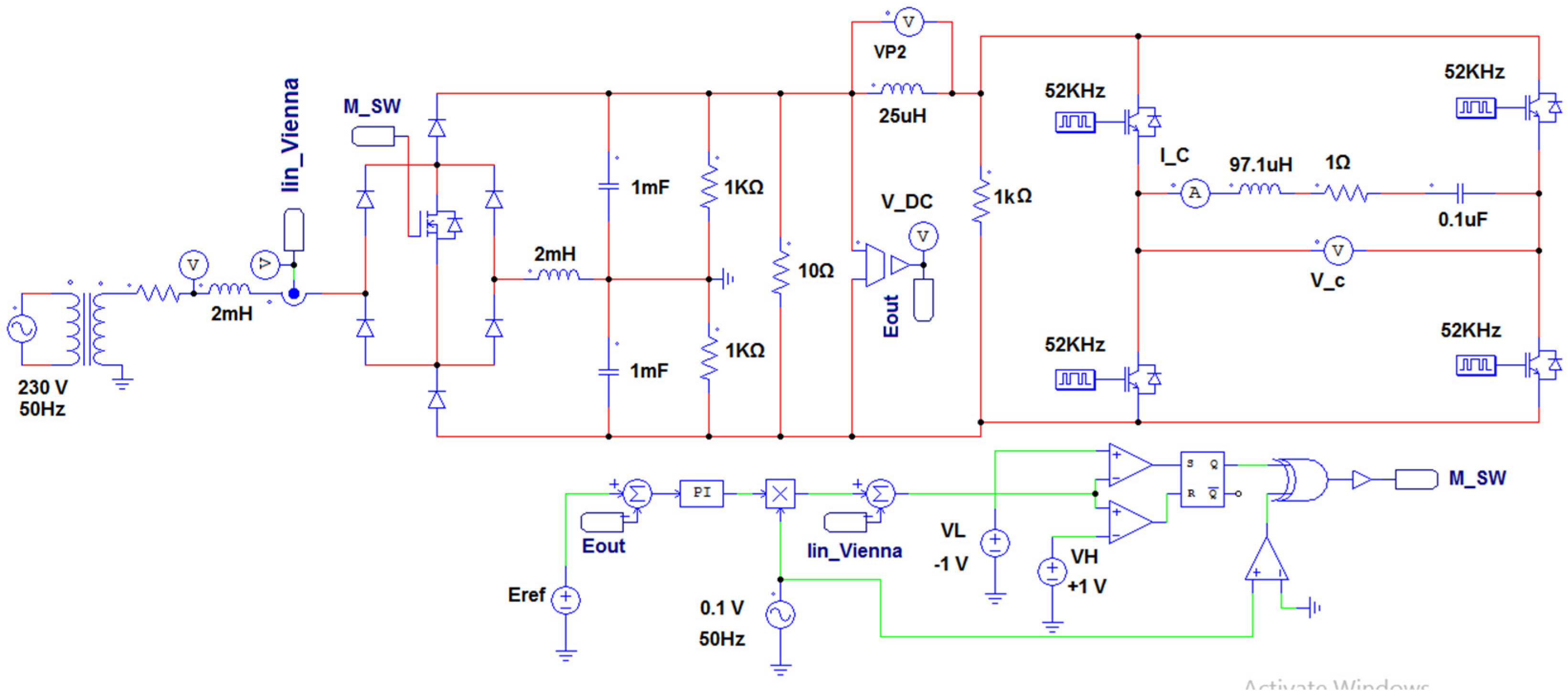
Over the last few years, Vienna rectifiers (VR) have emerged as a very good option for addressing the majority of the aforementioned issues. They were originally developed by a group of researchers headed by Professor Johann W. Kolar at the University of Vienna in the year 1993 [
20].They were initially invented as three-phase boost rectifiers and later developments led to the wide popularity of the single-phase configuration as well. In a conventional VR, the two capacitors present at the output split the output DC bus voltage, but in extremely unequal parts [
21]. It drastically fails to maintain the voltage across each capacitor balanced at the DC bus. As a result, the latter suffers from considerably high DC ripples, and overall, it results in an increased THD of the input current [
22]. In the conventional VR, only one capacitor receives energy from the source at a time, while the other capacitor keeps discharging during that period. The upper capacitor receives energy during the positive half-cycle of the input voltage, while the lower capacitor receives energy during the negative half-cycle. Thus, it is practically impossible to maintain a balanced and uniform voltage across both the capacitors present at the output DC bus [
23]. Moreover, the bulky size of the capacitors at the output of the VR remains a big problem in almost all the past topologies reported in the literature. Ali et al., in 2019, used bulky output capacitors of 10 mF each for C
1 and C
2 at the output of a VR [
24]. Rajaei et al., in 2014, used 22 mF capacitors for both C
1 and C
2 at the output of a VR [
25]. Najafi et al., in 2014, used 6.6 mF capacitors for both C
1 and C
2 at the output of a VR [
26].
The Modified Vienna rectifier (MVR) that is proposed in the present work overcomes all the aforementioned limitations that are present in the conventional VR. In the former, there is a transfer of energy to both of the capacitors during the positive and negative half-cycles of the input voltage. The conventional VR is only a boost-type rectifier, while the proposed MVR is enriched with a buck–boost effect, in addition to the boost effect that is present in its conventional counterpart. The proposed MVR maintains a balanced voltage for both of the capacitors present at the output DC bus. Thus, there will a considerable reduction in the ripple present at the output DC bus of the MVR. Due to this, a lesser value of the capacitors (1 mF) can be taken by the proposed MVR in comparison to the conventional VR. Additionally, there is a considerable reduction in the THD of the input current in the proposed MVR, due to the aforementioned benefits.
The proposed MVR topology comprises six diodes and only one active switch (MOSFET). As a result, the voltage on the individual component is quite low and, in each interval, just half of the DC bus voltage has to be dealt with. The power losses are identical for the various diodes; thus, they have nearly equal voltage ratings. However, for the sake of simplicity, it is assumed that the power switching devices have an ideal behavior. In practice, several efforts have been made toward developing accurate models that take into account the parasitic components of both, i.e., the diodes and the power MOSFETs [
27,
28,
29].
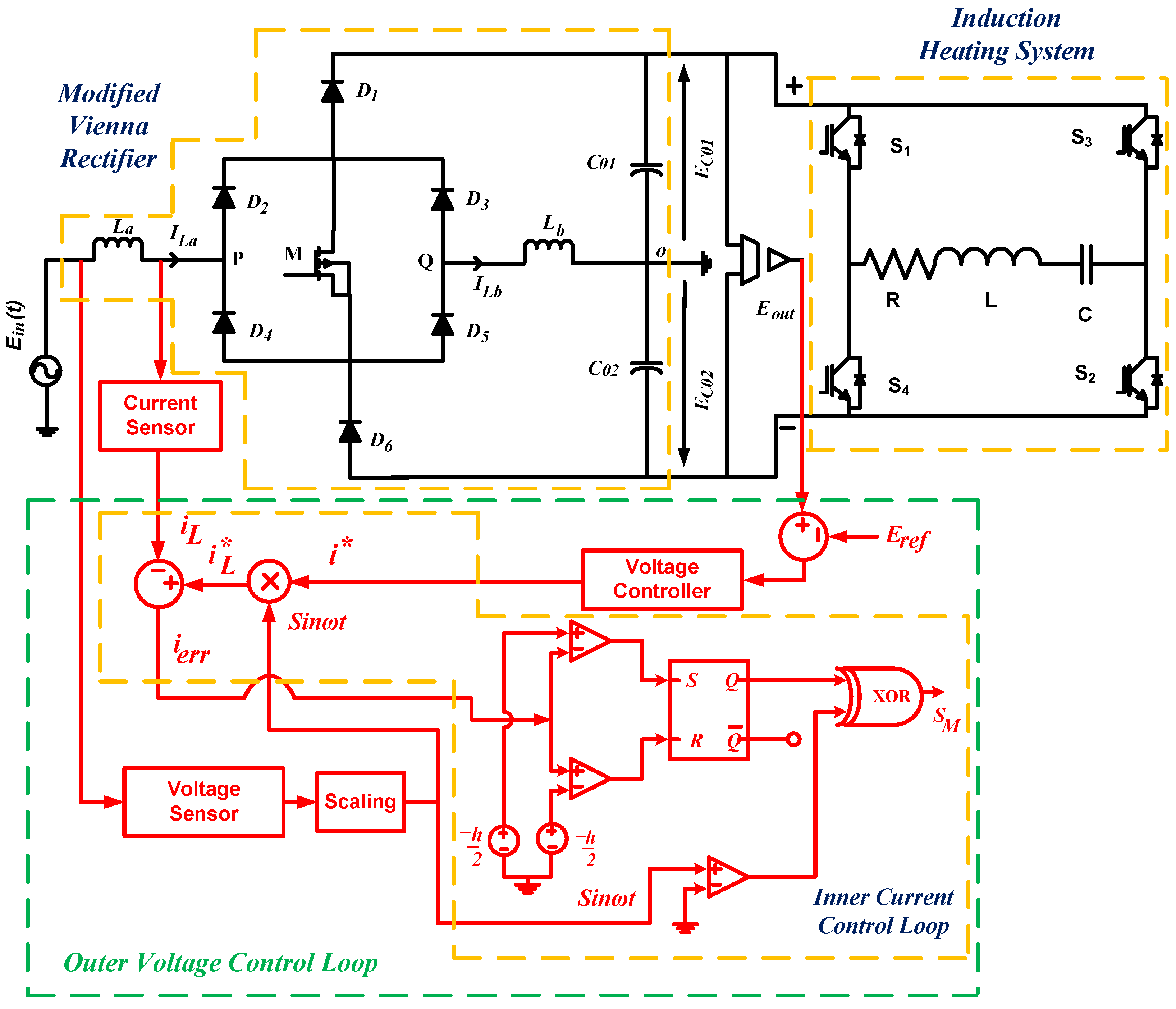
2. Proposed Structure of MVR Based IH System
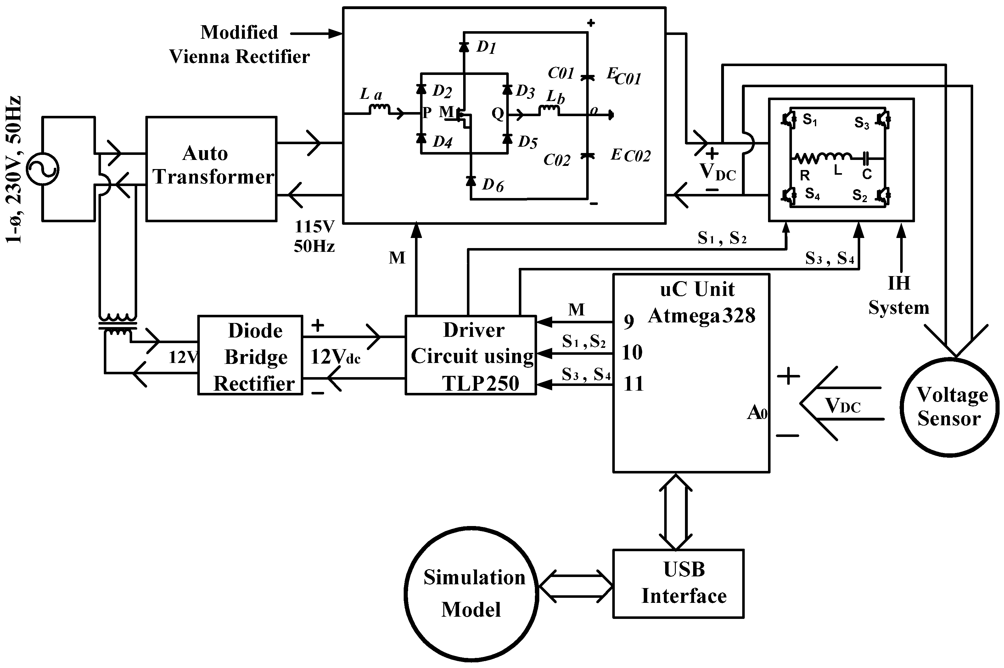
A block diagram of the complete IH system with the MVR, including a control circuit, is shown in
Figure 1. The controller consists of an outer voltage control loop, along with an inner current control loop. The voltage controller in the former consists of a PI controller, which is fed by the error between the sensed value of the DC link voltage and the reference DC link voltage. The voltage controller generates the reference current i*, which is multiplied by the waveform Sin(ɷt) of the input ac voltage. The latter can be obtained by simply dividing the sensed input voltage by its magnitude. After the aforesaid multiplication, it generates the final line current reference i
L*, which is compared with the sensed line current i
L to generate the current error i
err. Their error acts as an input for the hysteresis controller, which, in turn, generates the switching pulses for the MOSFET switch M of the MVR. The i
err is compared with the upper and lower bands of the hysteresis controller, which are represented by +h/2 and −h/2, respectively. When the i
err is more than the h/2, there will be a decrease in the input line current because of the zero gate current. When the i
err is less than the h/2, there will be gate signals in a high state, which, in turn, increases the input line current and the process repeats itself. The output of the hysteresis controller is fed to the SR flip-flop. The latter ensures that the MOSFET M remains in an OFF state, even when the current is reduced to below (i
L* +h/2). The output of the upper band of the hysteresis controller is given to the reset input (R), while that of the lower band is given to the set input (S) of the SR flip-flop. Afterward, it is fed to the XOR gate, whose other input is the scaled ac line voltage waveform that is passed through the comparator. The latter detects the positive half-cycle of the waveform and generates PWM signals of 50 Hz and a 50% duty cycle. The XOR gate finally generates PWM pulses of different frequencies, which are fed to the switch in the MVR.
3. Operation of the Proposed Single-Phase MVR
The MVR has been assumed to be unloaded for the sake of simplicity. When the input ac voltage is positive and the switch is closed, the energy stored in the inductances, La and Lb, increases. During this time, there is an increase in the capacitor voltages, EC01and EC02, and the MVR operates in power factor correction mode. When the switch M is open, the current passes through the capacitor C01 and the voltage across the capacitor C02 remains unchanged.
In the present work, the proposed topology of the MVR allows for the transfer of energy to both the capacitors, C01 and C02. Due to this, both boost and buck–boost effects are obtained simultaneously, which is explained from the mathematical model described below. The following will be demonstrated in the proposed MVR topology:
- (a)
When the input ac voltage is positive, the capacitor voltage EC01 has the boost effect, while the capacitor voltage EC02 has the buck–boost effect.
- (b)
When the input ac voltage is negative, the capacitor voltage EC01 has the buck–boost effect, while the capacitor voltage EC02 has the Boost effect.
In the present work, the operational analysis of the single-phase MVR was performed when the input voltage was positive as well as negative.
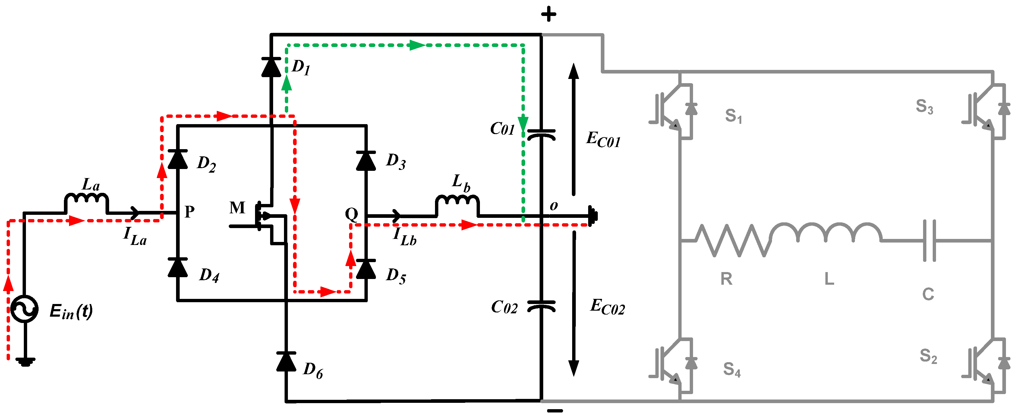
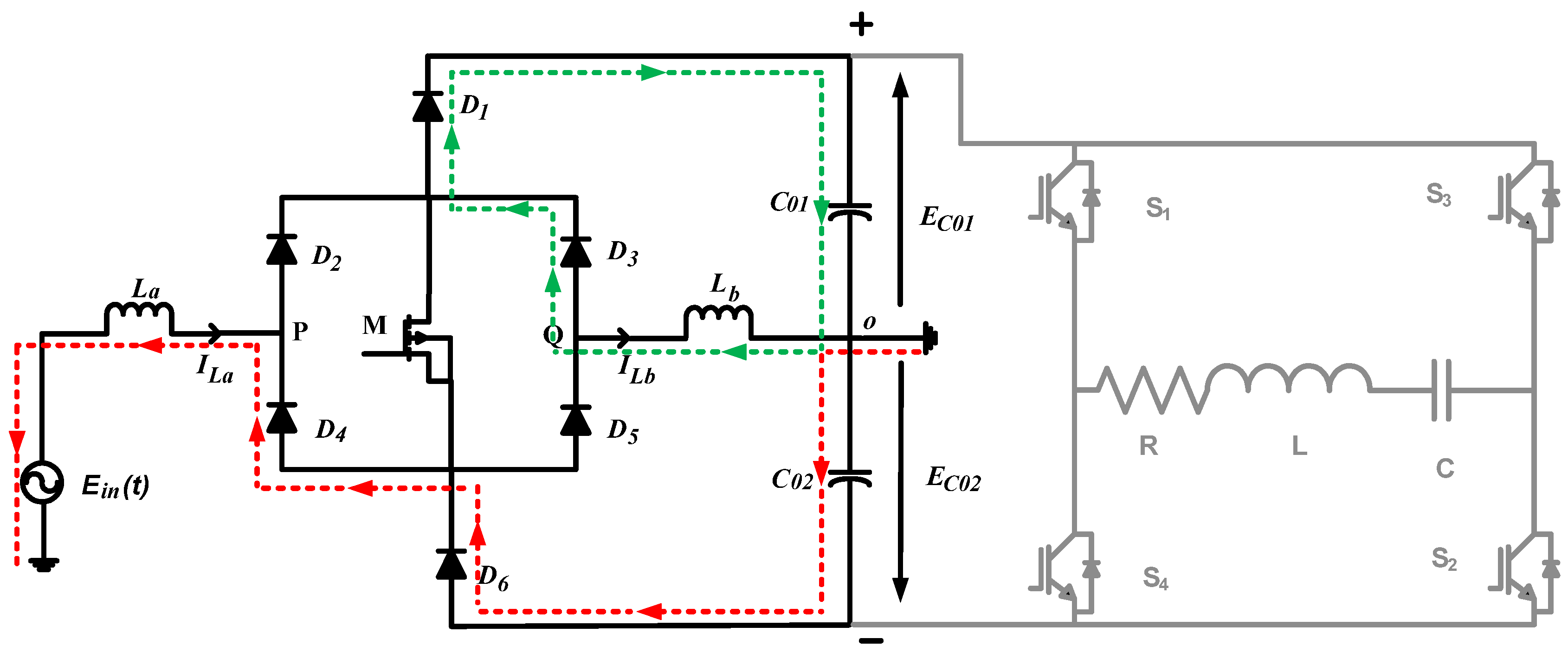
3.1. When the Input Voltage Is Positive and Switch Is Closed
As indicated in
Figure 2, when the input voltage is positive and the switch M is closed, there is a flow of current through the inductor L
a, the diode D
2, the switch M, the diode D
5, and the inductance L
b. The voltages at points P and Q, represented by V
P and V
Q, are equal. Thus,
For a short span of time, some part of the current I
La(t) flows in the positive DC bus and the diode D
1 is forward-biased.
After that, the current in the inductors L
a and L
b becomes equal and the diode D
1 becomes OFF. Then,
The condition of the other diodes can be expressed by the following equations.
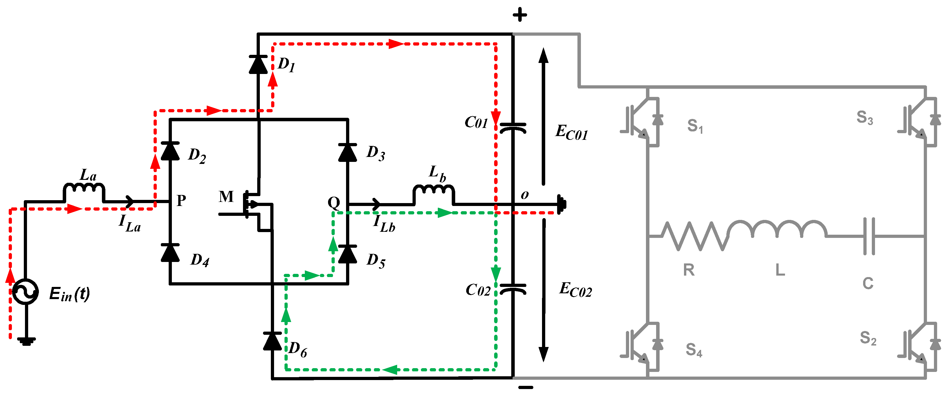
3.2. When the Input Voltage Is Positive and Switch Is Open
As depicted in
Figure 3, there are two current paths in the open state of the switch. The current coming from the supply passes through the inductor L
a, the diodes D
2 and D
1, and the capacitor C
01.Since the diodes D
2and D
1 are in the conducting states, the voltage of point P (V
p) becomes equal to the positive DC bus voltage.
The diodes D
5 and D
6 are also forward-biased and in conducting states. Therefore, the voltage of point Q (V
Q) and the voltage of the negative DC bus become equal. Thus,
The switch M and the diodes D
3 and D
4 are in the OFF state, so there are voltages across these components. If V
M(t) is the voltage across the switch and i
M(t) is its current, then,
3.3. Model of MVR under Positive Input Voltage Condition
Considering the circuit shown in
Figure 3, the following equations can be verified.
where V
P and V
Q are the voltages at points P and Q, respectively.
The currents iLa and iLb flowing in the inductors La and Lb, respectively, are assumed to be under control and have a negligible phase shift with the input voltage. If D is the duty cycle and T is the time period of the MOSFET switch M, then it remains closed for DT and open for (1 − D)T span of time. The open-switch operation can be explained as follows:
Using Equations (13) and (21), we obtain:
Using Equations (23) and (24), we obtain:
Multiplying both sides by (1 − D), we obtain:
Similarly, the closed-switch operation can be depicted by the equation given below.
A function of i
La for the complete period T in the positive input voltage condition can be obtained by adding Equations (26) and (27) as follows:
In the same manner, a function of the inductor current i
Lb for the complete period T in the positive input voltage condition can be obtained by using Equation (20) as follows:
Equation (28) can be used to obtain an expression for EC01(t)/Ein(t) in the positive input voltage condition as follows:
Then, using Equations (28) and (30), we obtain:
Inputting the value of r from Equation (30) into Equation (37), we obtain:
Again, Equation (29) can be used to obtain an expression for E
C02(t)/E
in(t)) in the positive input voltage condition as follows:
Then, using Equations (29) and (39), we obtain:
Inputting the value of u from Equation (39) into Equation (44), we obtain:
Equations (38) and (45) can be summarized together to deduce some important conclusions for the positive input voltage condition as follows:
The upper equation (obtained in Equation (38)) involves a boost effect on the positive DC bus, while the lower equation (obtained in Equation (45)) involves a buck–boost effect on the negative DC bus. The magnitude of these effects also depends upon the values of the inductances La and Lb. The DC ripple at the output of the MVR is greatly reduced due to these effects. The aforementioned results can also be used for the conventional “VIENNA I” rectifier by making the value of inductance Lb equal to zero. However, in that case, the buck–boost effect does not take place and there is a transfer of energy only to the capacitor C01, and not to the capacitor C02.
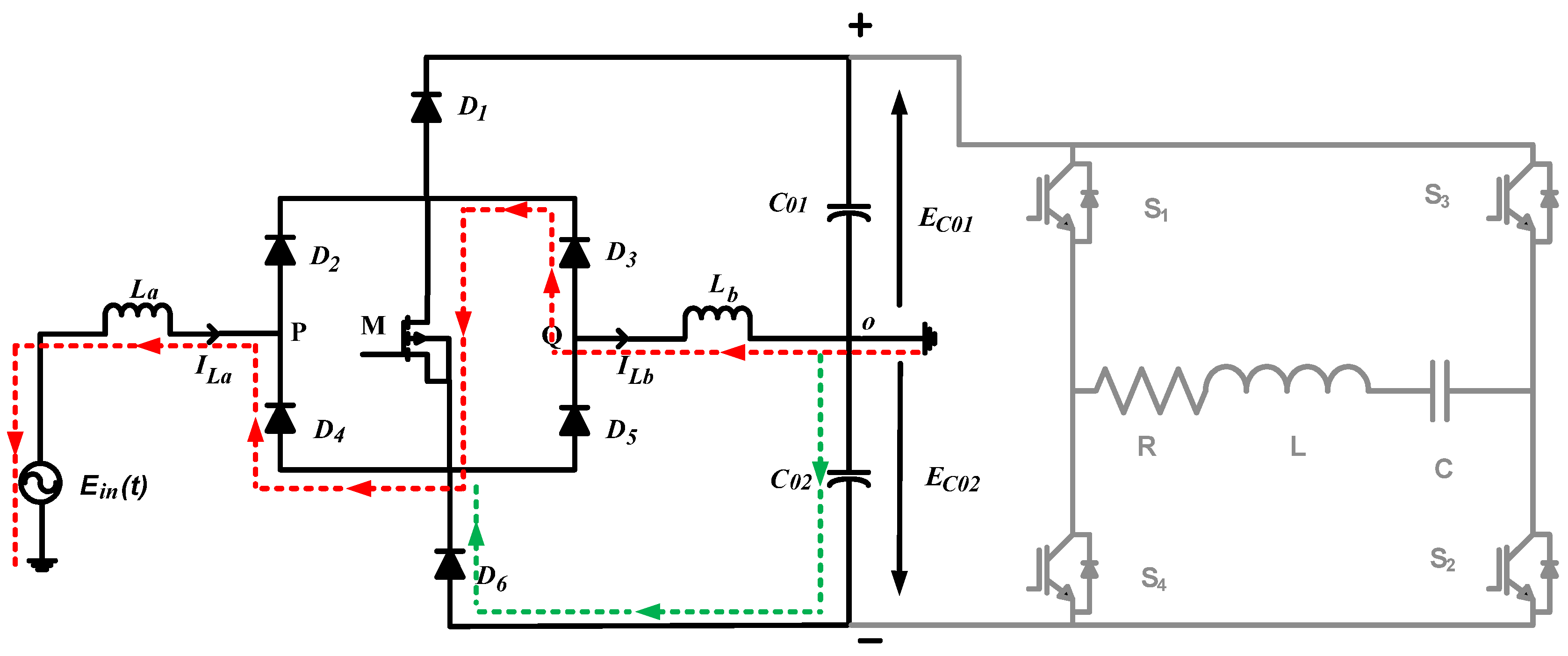
3.4. When the Input Voltage Is Negative and Switch Is Closed
In the present case, the input voltage is negative and the switch M is in the closed condition. The current path is negative and it passes through the inductance L
b, the diode D
3, the switch M, the diode D
4, and the inductance L
a. The direction of the currents i
La and i
Lb flowing in the inductances L
a and L
b, respectively, are assumed to be from left to right, as indicated in
Figure 4. This is in the opposite direction to the actual current flowing in the circuit. Moreover, a current also flows in the diode D
6 and the capacitor C
02, as indicated in
Figure 4. As the diodes D
3 and D
4 are in the ON state, along with the switch M, V
p becomes equal to V
Q. Thus,
Some part of the current i
La flows in the negative DC bus, and for a short span of time, the diode D
6 is in the ON state.
Thereafter, the currents i
La and i
Lb flowing in the inductors L
a and L
b, respectively, become equal, and the diode D
6 goes into the OFF state. As a result:
The conditions of the other parts of the circuit can be explained by the following equations given below.
3.5. When the Input Voltage Is Negative and Switch Is Open
There are two paths for the current when the input voltage is negative and the switch is open, as shown in
Figure 5. In the first path, the current flows through the capacitor C
02 and the diodes D
6 and D
4, as well as the inductor L
a. Since the diodes D
4 and D
6 are in the ON state, the voltage of point P (V
P) becomes equal to the voltage of the negative DC bus. Thus,
The other path of the current is through the capacitor C
01, the inductor L
b, and the diodes D
3 and D
1, which are forward-biased. As a result, the voltage of point Q (V
Q) becomes equal to the positive DC bus voltage. Thus,
Additionally, the switch M and the diodes D
2 and D
5 are in the OFF state. So,
3.6. Model of MVR under Negative Input Voltage Condition
Considering the circuit shown in
Figure 5, the following equations can be verified for the open-switch operation under the negative input voltage condition.
Using Equations (21) and (58), we obtain:
Inputting the value of Equation (23) into Equation (65), we obtain:
Multiplying both sides by (1 − D), we obtain:
Similarly, the closed-switch operation for the negative input voltage condition can be depicted by the equation given below.
A function of i
La for the complete period T in the negative input voltage condition can be obtained by adding Equations (67) and (68) as follows:
In the same manner, a function of the inductor current i
Lb for the complete period T in the negative input voltage condition can be obtained as follows:
Equation (70) can be used to obtain an expression for EC01(t)/Ein(t) in the negative input voltage condition as follows:
Then, Equation (70) can be written as follows:
Inputting the value of u from Equation (39) into Equation (75), we obtain:
Again, Equation (69) can be used to obtain an expression for EC01(t)/Ein(t) in the negative input voltage condition as follows:
Then, using Equations (30) and (69), we obtain:
Inputting the value of r from Equation (30) into Equation (83), we obtain:
Equations (76) and (84) can be summarized together to deduce some important conclusions for the negative input voltage condition as follows:
The upper equation (obtained in Equation (76)) involves a buck–boost effect on the positive DC bus, while the lower equation (obtained in Equation (84)) involves a boost effect on the negative DC bus. The magnitude of these effects also depends upon the values of the inductances La and Lb. The DC ripple at the output of the MVR is greatly reduced due to these effects. Similar to the positive input voltage condition, the aforementioned results can be used for the conventional “VIENNA I” rectifier by making the value of inductance Lb equal to zero. However, in that case, the buck–boost effect does not take place and there is a transfer of energy only to the capacitor C02, and not to the capacitor C01.
Thus, there is a transfer of energy to both of the capacitors during the positive and negative input voltage conditions. In the conventional “VIENNA I” rectifier, the upper capacitor C01 receives energy during positive input voltage, while the lower capacitor C02 receives energy during negative input voltage. Therefore, there was only a boost effect in both cases. However, in the proposed MVR topology, a buck–boost effect takes place, along with the boost effect that is present in the conventional “VIENNA I” rectifier. The DC ripples in the former are considerably lesser than those in the latter, even if the sum of the inductances La and Lb is equal to that in the conventional “VIENNA I” rectifier and the other parameters are identical. Moreover, a lesser value of the capacitors C01 and C02 can be employed in the present case in comparison to the conventional one.
4. Maximum Switching Frequency (MSF) Analysis of Hysteresis Controller
Figure 6a,b show the hysteresis current control under the normal and worst case conditions, respectively. The latter is taken into consideration for the calculation of the maximum switching frequency (MSF) of the HCC. As it was already mentioned in
Section 2, the difference in the reference current (i
L*) and actual current (i
L) acts an input to the HCC, where it is denoted by i
err. It is compared with the upper band (i
L* + h/2) and lower band (i
L* − h/2) of the HCC. When the actual current becomes more than the upper band, then there will be a decrease in the actual current, which is achieved by making the gate signal zero. Again, if the actual current falls below the lower band, then it is increased by making the gate signal high. This process repeats itself again and again and, as a result, the actual current stays within the hysteresis tolerance band (h), as shown in
Figure 6a. The output of the HCC acts an input to the SR flip-flop, which is further fed to the XOR gate. The other input of the XOR gate is the scaled ac line voltage waveform that is passed through a comparator. The latter is responsible for detecting the positive half-cycle of the input ac voltage, as well as the generation of PWM pulses that have a duty cycle of 0.5 and a frequency of 50 Hz. The XOR gate finally produces PWM pulses of variable frequencies, governed by the rate at which the actual current varies in the hysteresis tolerance band.
Under the worst case condition shown in
Figure 6b, there will be a very sharp increase in the actual current flow. It reaches from point C to point B in time Ta= CA, which is the minimum turn ON time of the switch. Here, it becomes important to explain the slope of the reference current.
where,
fref = the frequency of the reference current.
P = the peak value of the sinusoidal reference current.
Let DB be a line parallel to CA. A tangent is considered at point t = T/2 on the reference current and BE is assumed to be parallel to this tangent. Applying the basic principles of geometry to
Figure 6b, we obtain:
where, h is the hysteresis tolerance band.
T
a can be approximately expressed as follows:
where m is the slope of the reference current.
If T
b is assumed to be equal to T
a, then the maximum switching frequency of the hysteresis controller (HC) can be expressed as follows:
For digital implementations, the discrete time intervals are used for collecting the samples. The slope of the reference current (m) can be expressed as follows:
where:
Using Equations (90) and (91), we obtain:
While considering the sinusoidal hysteresis band for the worst condition analysis, both T
a and T
b may be just one sampling interval.
5. Design Procedure for Parameter Selection
5.1. Equivalent Circuit Parameter Model of IH System
The magnetic field of a coil can cause an eddy current in a nearby conducting surface when an alternating current runs through the coil. The effective impedance of the coil is established by the loading that is imposed by the magnitude and phase of this produced eddy current. The process of induction heating occurs via electromagnetic induction. In order to evaluate the effectiveness of a cooker that uses induction heating, it is necessary to design an equivalent circuit that accurately depicts the phenomena involved in induction heating. The equivalent inductance of a home induction cooker relies heavily on the size and material of the cooking pan being used. Thus, the induction coil’s layout is crucial to the performance of any induction cooker.
This section explains how an equivalent circuit parameter model of the proposed induction cooker was developed, which is a necessary step before the design of the induction coil can begin.
The formula for calculating the resistance of the coil, denoted by “R
IH,C,” is as follows:
where:
ρmat = the resistivity of the material that makes up the induction heater’s coil.
lc = the length of the conductor used in the induction heater’s coil.
rc = the radius of the conductor used in the induction heater’s coil.
δ = the skin depth of the induction heater’s coil conductor
The calculation of the self-inductance of a flat-pancake-type heating coil can be performed as follows, with the use of Wheeler’s formula:
where,
LIH,C = the self-inductance of the induction heater’s coil.
NIH,C = the number of turns present in the induction heater’s coil.
Z = the average radius of the induction heater’s coil.
C
IH,w = the width of the induction heater’s coil.
where:
x = the inner radius of the induction heater’s coil.
y = the outer radius of the induction heater’s coil.
Using Equations (95)–(97), we obtain:
The IH coil and pan (work-piece) are analogous to a transformer where the heating coil serves as its primary winding, while the cooking pan serves as the closed secondary winding. The resistance of the pan changes with the temperature, however, for the purpose of domestic IH, it is almost negligible, and the equivalent circuit parameter model works with a good accuracy. Many past studies have confirmed the wide acceptance of this method of analysis within the electrical domain.
The heating coil has its own self-inductance, which is denoted by L
IH,C. The heating coil and the cooking pan have a mutual inductance, which is denoted by M
IH. As there is no actual winding on the cooking pan side, the inductance of the IH pan, referred to the coil side, is equal to the mutual inductance, M
IH. An analogous series combination of the resistance and inductance can be used to represent both the heating coil and the cooking pan, also known as the load. They are expressed as follows:
where:
RPan,CS = the effective resistance of the pan referred to the coil side.
RIH,C = the resistance of the induction heater’s coil.
RIH,total = the total resistance measured on the side of the heating coil.
LIH,C = the self-inductance of the induction heater’s coil.
LIH,total = the total inductance measured on the side of the heating coil.
In induction heating (IH) systems, the resistance of the pan referred to the coil side is the same as its magnetizing reactance. Thus, k
2 = 0.5.
From the experiments analysis performed by Sadhu et al., 2012 [
30], the parameters such as the resistance and inductance of the coil and the mutual inductance, etc., are as follows:
RIH,C = 0.055 Ω, RPan,CS = 1.89 Ω, LIH,C = 101.62 µF, MIH = 9.03 µF, and CIH = 0.1 µF.
Inputting these values into Equations (103) and (104), we obtain:
As already mentioned in the introduction section, the work-coil and work-piece (cooking pan) are modeled as a series combination of the resistor and inductor, while an external capacitor is used for achieving the resonance condition. The resonant frequency is calculated as follows:
The switching frequency (f
I,sw) of the high-frequency inverter of the IH system is kept slightly higher than the resonant frequency of the IH load. This is to ensure the zero voltage switching (ZVS) condition in the IH system, and it is a very popular and time-tested method. Therefore,
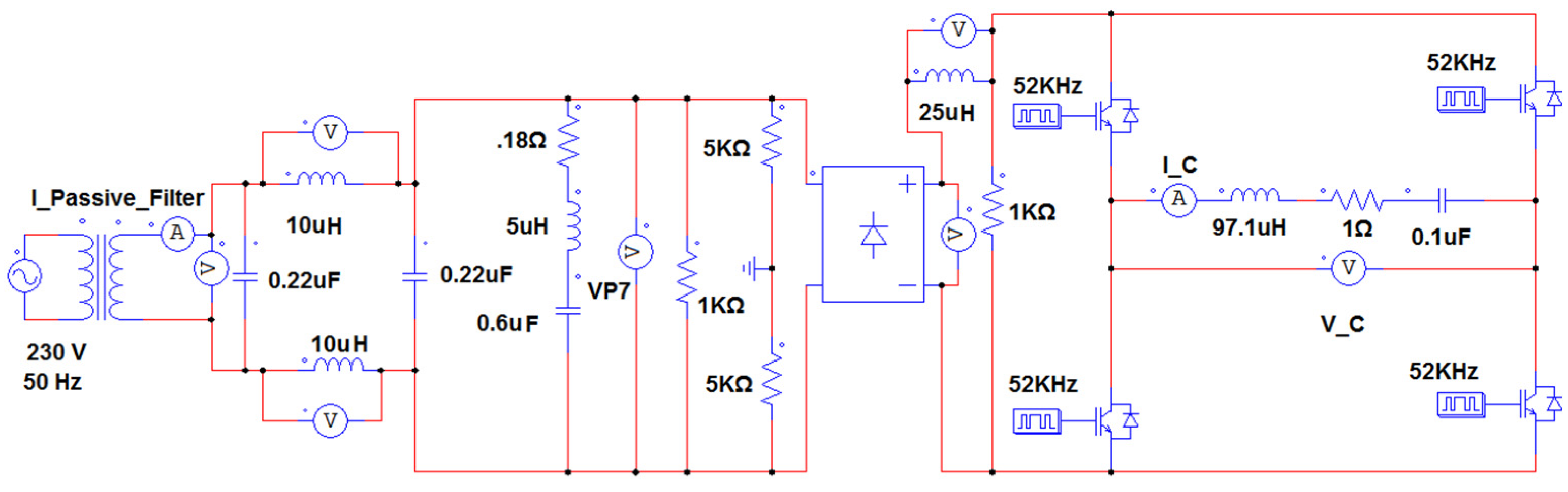
5.2. Ring-Type Passive Filter
Figure 7 shows the basic structure of a ring-type passive filter. The equivalent reactance of the passive filter by looking from the input side can be expressed as follows:
In the resonance condition, when the inductive component balances the capacitive component, then, Xp will be theoretically infinite and practically very high. Thus, the cutoff frequency of the passive filter can be determined, and above this frequency, the harmonic components are blocked. The resonant frequency of this passive filter is expressed as follows:
Various parameters are taken into consideration while designing these passive filters. Some of the predominant ones are the ripple factor, the cut-off frequency, and the rate of attaining a final roll off, etc.
Pal et al., 2015 [
12] performed a detailed analysis of ring-type passive filters. They deduced some important expressions which can be used to calculate the inductance and capacitance of ring-type passive filters, which are as follows:
where:
ZCI = the characteristic impedance of the passive filter.
fcut-off = the cut-off frequency of the passive filter.
Taking f
cut-off = 2.15 KHz, Z
CI = 0.067 Ω [
12], and inputting the values into Equations (112) and (113), we obtain:
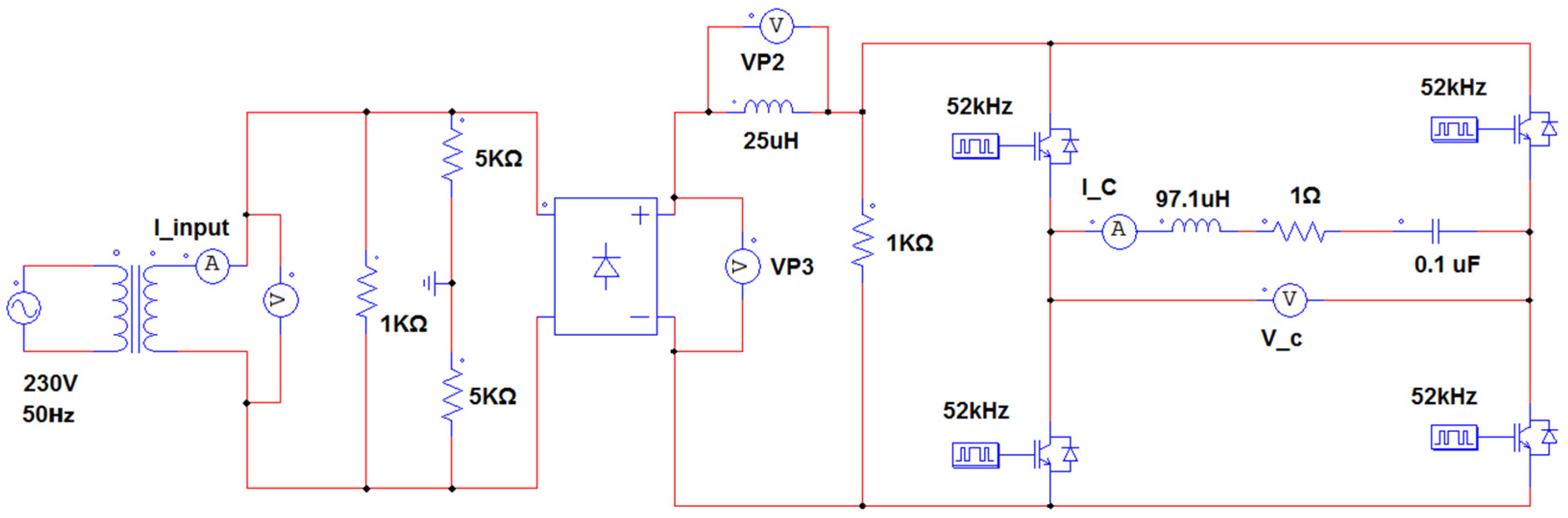
7. Experimental Setup of the Proposed MVR Based IH System and Its Analysis
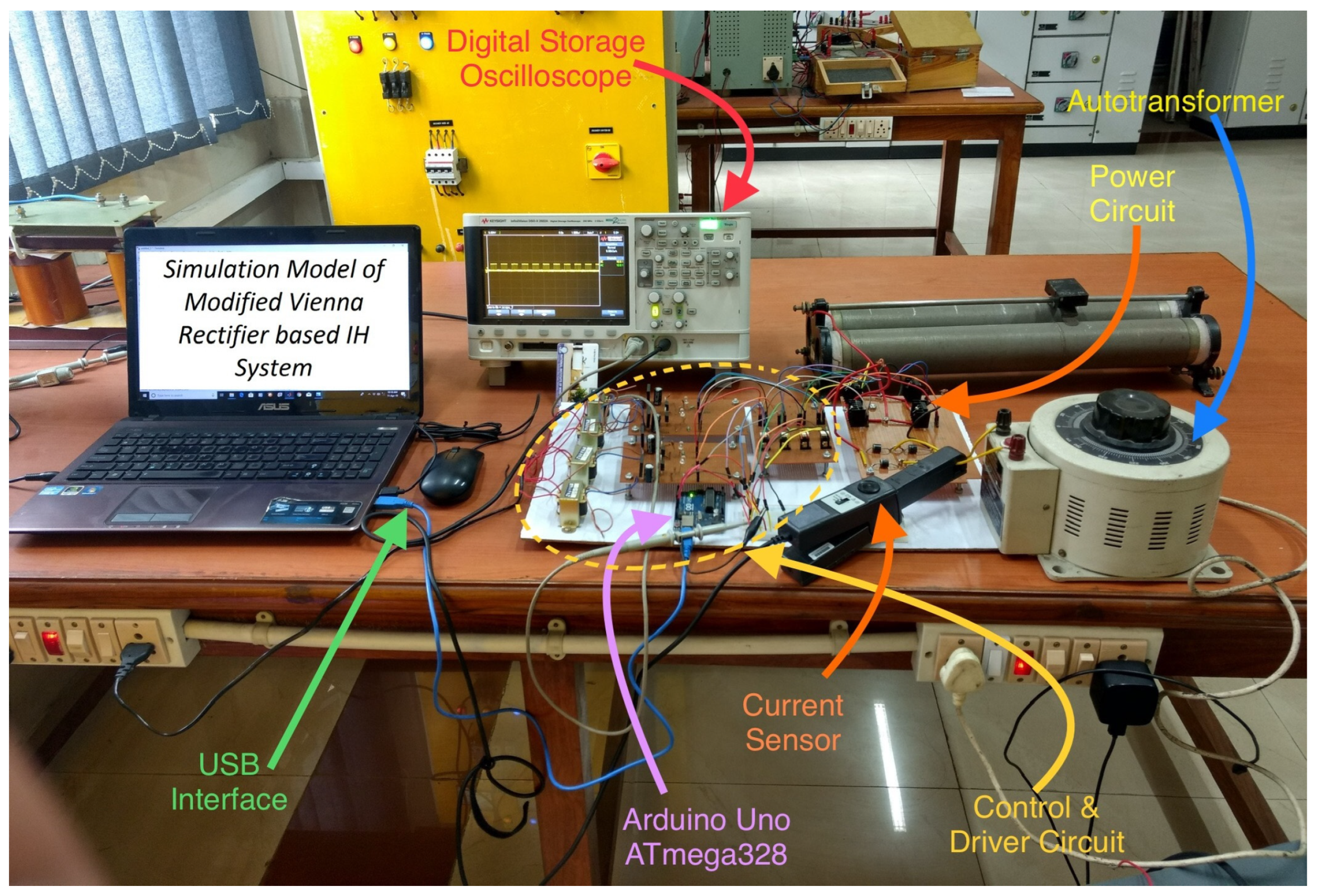
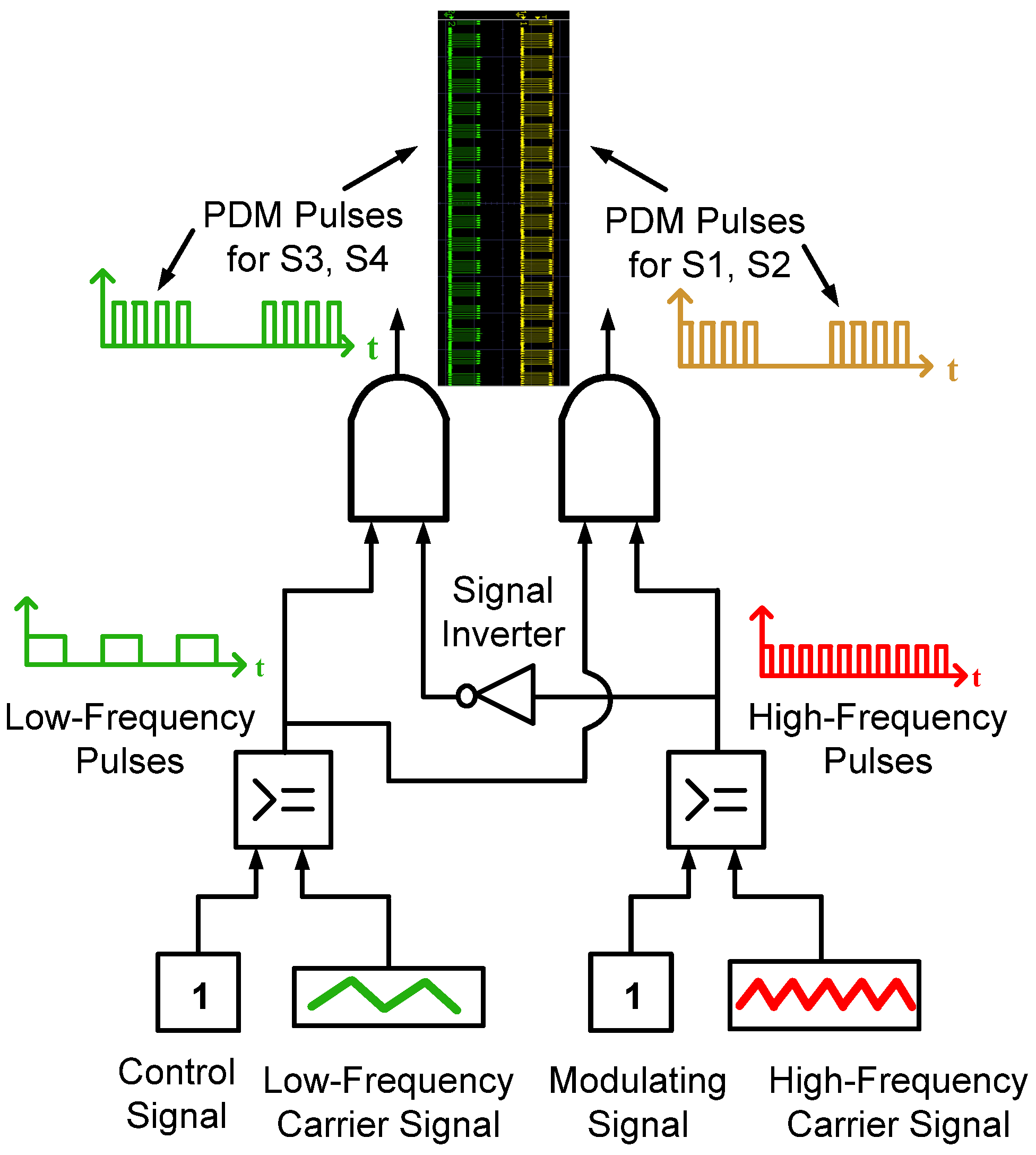
The experimental validation of the proposed model has been performed by developing a prototype of the proposed MVR and the 1200 W IH system in the power electronics lab of the Indian Institute of Technology (ISM), Dhanbad, India. The aforementioned prototype uses an Arduino Uno (Atmega 328)-based digital controller. A general layout diagram of the basic structure of the experimental setup is shown in
Figure 20, while
Figure 21 shows the complete experimental setup. The structure of the pulse density modulation (PDM) controller, which was employed for the generation of the PWM pulses, is shown in
Figure 22.
The pulses obtained from the support package are fed to the Arduino board. First of all, an ac input voltage of 230 V at 50 Hz is converted to 115 V at 50 Hz by using an auto-transformer, then it is fed to the MVR. The latter has a boost and a buck-boost effect; thus, it converts the 115 V at 50 Hz ac to a 327 V DC value. Thereafter, it is sensed by a voltage sensor and its magnitude is reduced under the 5 V range. Now, the controller present in the Arduino board generates the switching signals for the resonant inverter of the IH system, as well as the MVR. The Arduino board has a wide range of pin configurations, out of which, only the analog pin on the input side and the digital pins on the output side are used in the present case. The voltage sensor feeds the analog pin A
0 on the input side, while the digital outputs obtained from pins 9, 10, and 11, comprising the PWM pulses, are fed to the gate driver circuit. The output of the MVR after being scaled-down is not just fed to the analog pin A
0 of the Arduino board, but is also compared to the reference DC voltage. Finally, the switching pulses are generated for the IH system, as well as the MVR, as shown in
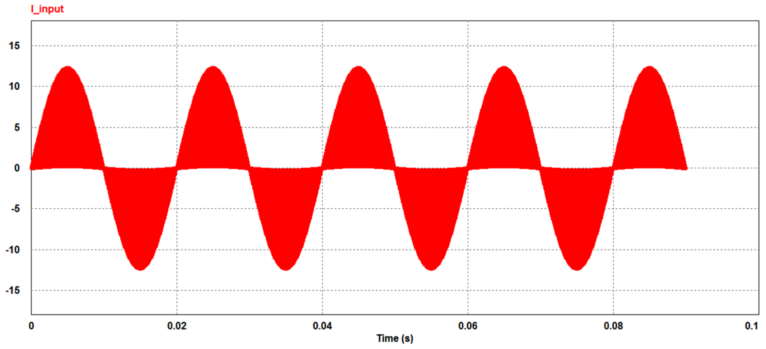
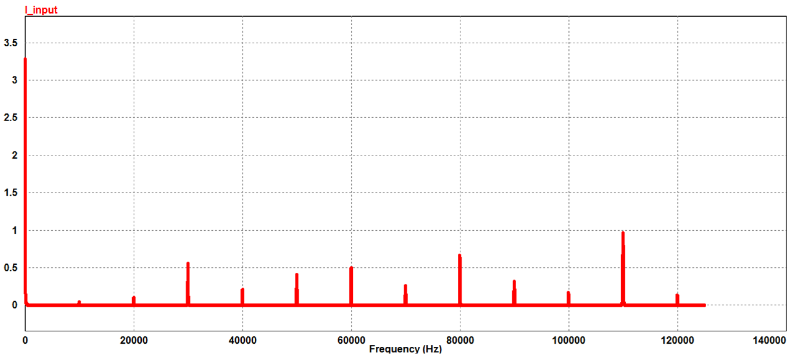
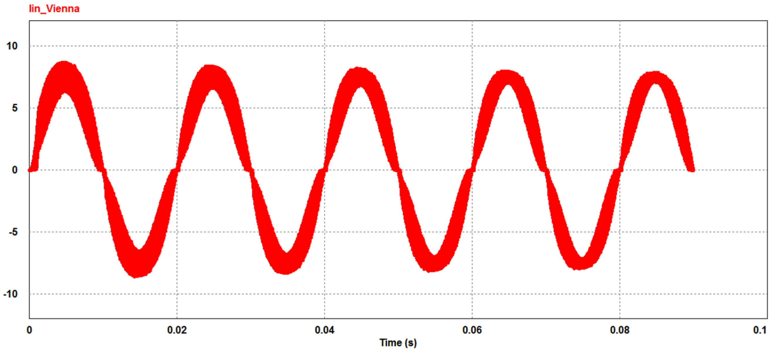
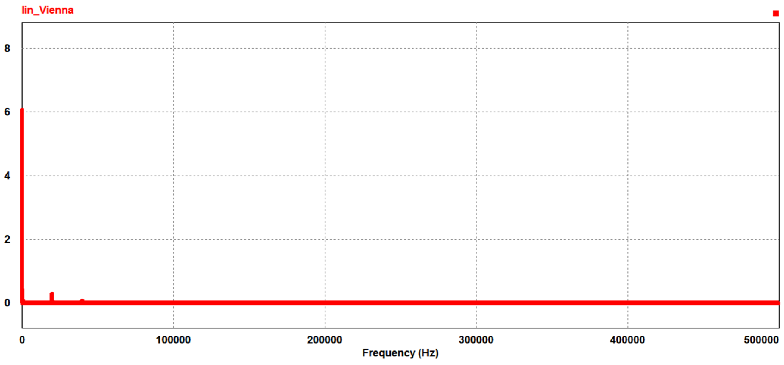
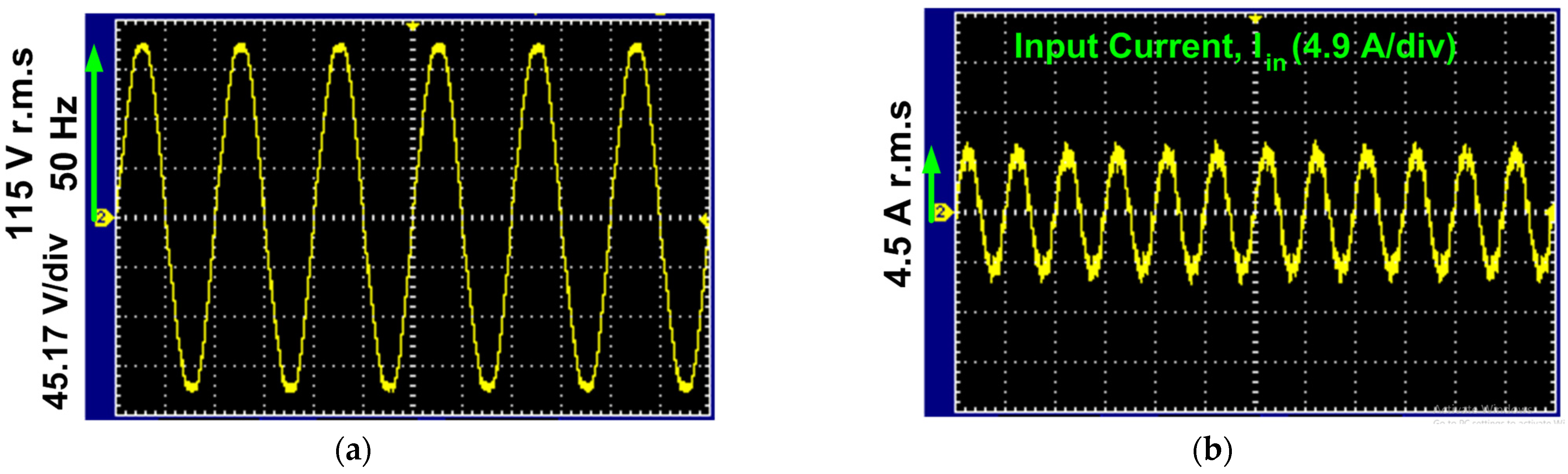
Figure 22The experimentally obtained input voltage and current are shown in
Figure 23. The list of components used for the experimental prototype implementation are shown in
Table A1 of
Appendix A. The harmonic distortions in the input current waveform were considerably reduced and the THD was found to be 4.26%, which follows the IEEE 519 standards. This is close to the THD value of 3.56% that was obtained from the simulation in PSIM. The power factor was nearly equal to 1 in the simulation, while it was recorded to be 0.95 in the experimental setup. The output DC bus voltage of the proposed MVR was 330 V from the simulations, while it was recorded to be 327 V experimentally, which are shown in
Figure 24a,b, respectively. This indicates that the proposed MVR was able to boost the input voltage and that the ripples were almost absent, which proved to be a serious limitation of the conventional VR. The output DC voltage of the conventional VR obtained from the simulation is shown in
Figure 24c. It was just 240 V, which is much less than the proposed MVR, which had a value of 330, while its pf was measured as just 0.93 against unity in the case of the proposed MVR.
At a given load condition (R
IH,total = 1 Ω), the input and output voltages were recorded to be 230 V and 226.5 V, respectively, while the input and output currents were found to be 4.5 A and 3.8 A, respectively. As already mentioned above, the power factors were found to be 0.95 and 1 at the input and output sides, respectively. The efficiency of the proposed MVR-based IH system for the given load (R
IH, total = 1 Ω) is as follows:
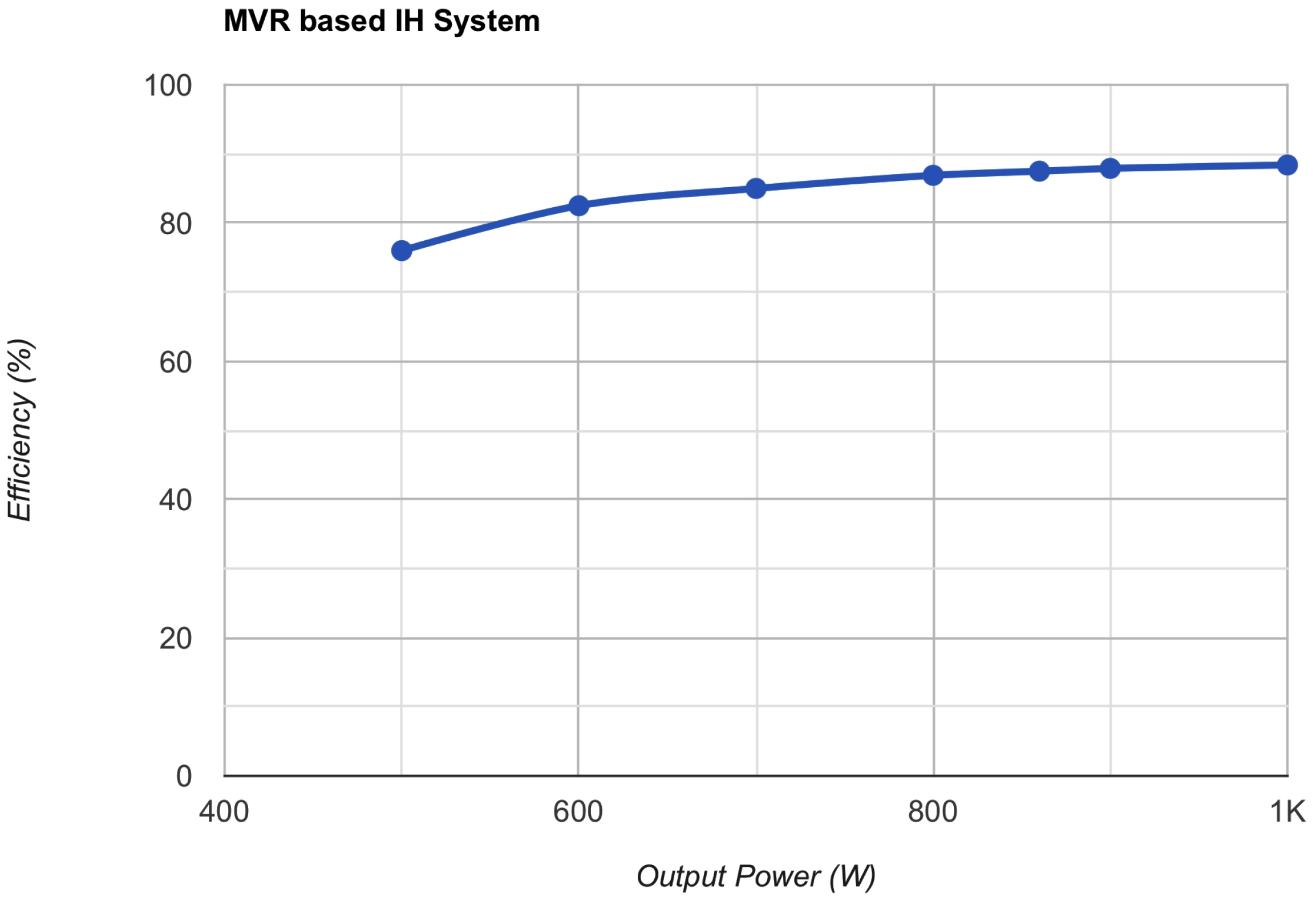
It was observed that the output voltage remained constant at 226.5 V when the load was changed. However, the output power kept on changing with a change in the load and the same was the case with the efficiency. Thus, a graph showing the relation between the output power and efficiency obtained by changing the load is shown in
Figure 25. It was observed that the efficiency improved with an increase in the output power.
8. Conclusions
In the present paper, a novel single-phase modified Vienna rectifier has been proposed for the power quality improvement of a domestic induction heating (IH) system. Moreover, a control strategy based on the hysteresis current control (HCC) scheme has also been proposed in the present work. It also includes a maximum switching frequency (MSF) analysis of the proposed HCC. An innovative method that uses the pulse density modulation (PDM) scheme for switching the power circuit of the IH has also been proposed for the experimental setup. A detailed design procedure has been discussed to calculate the load parameters based on the equivalent circuit model of the IH system. This is followed by an analysis of the ring-type passive filter and its parameter calculations. A detailed mathematical analysis of the proposed MVR has been performed in the switch ON and OFF states during the positive and negative input voltage conditions. The aforesaid analysis revealed that, in the proposed MVR, both of the DC bus capacitors received energy during the positive and negative half-cycles of the input voltage.
The biggest limitation of the conventional VR was the upper DC bus capacitor receiving energy during the positive half-cycle while the lower capacitor received energy during the negative half-cycle. Thus, the proposed MVR has an added buck–boost effect along with the boost effect that is present in the conventional VR. Due to this, the output DC voltage of the proposed MVR was found to be 330 V in the simulation and 327 V in the hardware setup. As a result of the aforementioned effects, the ripples present at the output DC bus of the MVR were almost absent. Another big limitation of the conventional VR was its high DC ripples limiting its use in many applications. This is evident from the output DC voltage waveform of the conventional VR, where a large ripple content and much lesser output voltage were observed. Moreover, due to this, capacitors of smaller values can be used in the proposed MVR. This is evident from the use of 1 mF capacitors at the output of the proposed MVR in comparison to the other topologies reported in the literature. Ali et al. [
24] used 10 mF, Rajaei at al. [
25] used 22 mF, and Najafi et al. [
26] used 6.6 mF capacitors at the output of the conventional Vienna rectifier.
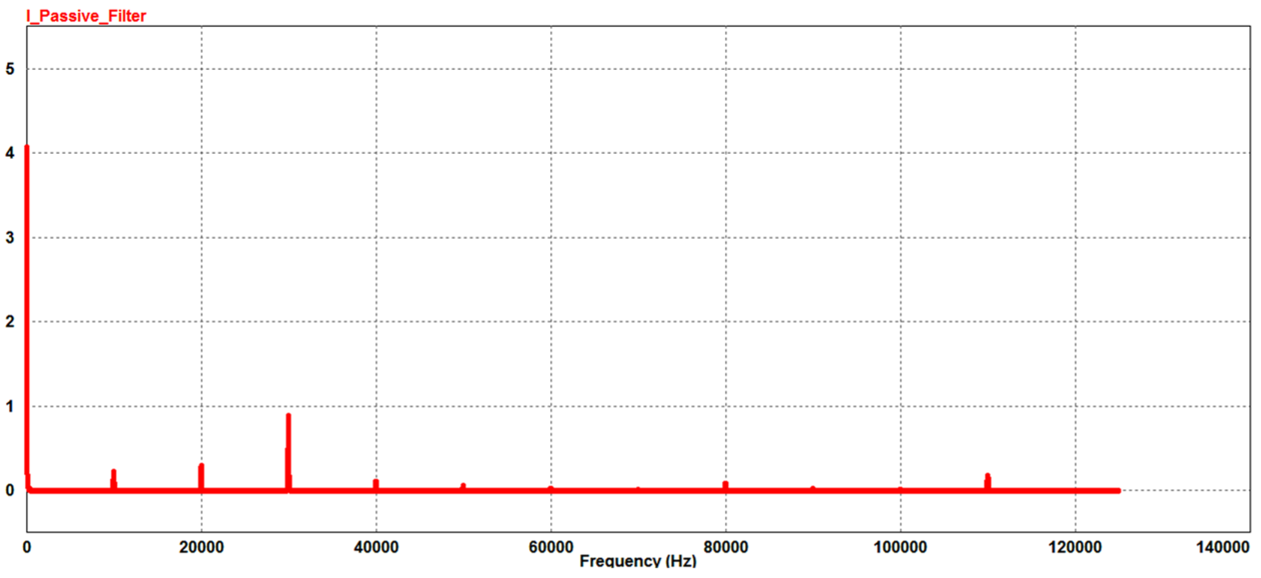
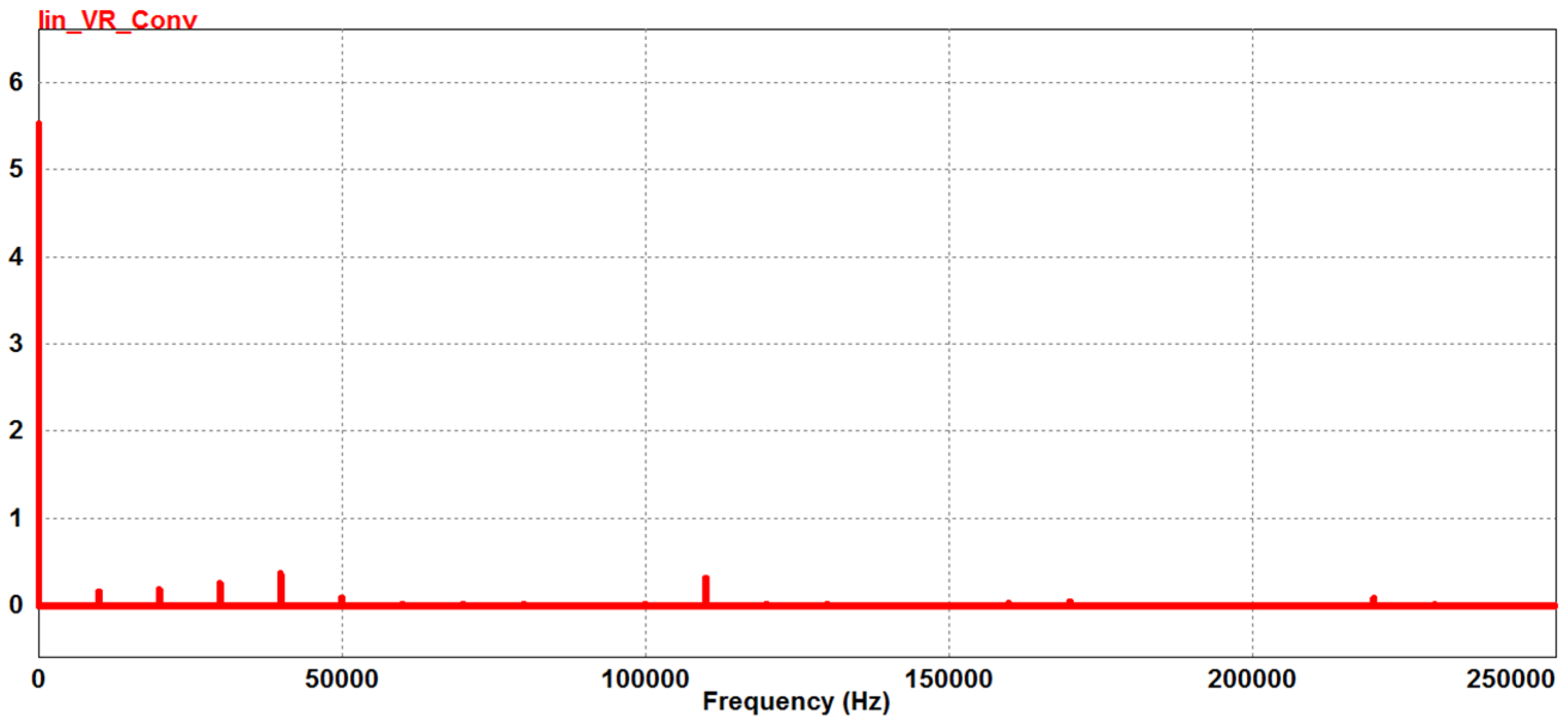
The THD in the input current waveform was found to be 46.60% without a filter and was reduced to 23.95% with a passive filter, while it was found to be 14.75% with the application of a conventional VR. None of these topologies were able to get the THD as per the harmonic regulations such as IEEE Std. 519-2014, IEC-555, and EN 61000-3-2, etc. However, with the application of the proposed MVR, it was found to be 3.56% and 4.26% in the simulation and experimental setup, respectively. The power factor was nearly equal to 1 in the simulation, while it was recorded to be 0.95 in the experimental setup. The simulation and hardware results of the power quality indices are as per the IEEE-519 standards, which justify the need for the proposed MVR in IH systems.
The efficiency of the proposed MVR-based IH system was also evaluated from the experimental setup. For a 1Ω load, the input and output voltages were recorded to be 230 V and 226.5 V, respectively, while the input and output currents were found to be 4.5 A and 3.8 A, respectively. The power factors were found to be 0.95 and 1 at the input and output sides, respectively. The efficiency was found to be 87.54% for the complete MVR-based IH system. It was observed that the output voltage remained constant at 226.5 V when the load was changed. However, the output power kept on changing with a change in the load, and the same was the case with the efficiency. It was also observed that the efficiency improved with an increase in the output power. Thus, the proposed MVR was able to address the majority of the limitations of conventional topologies and it may be used as an integral part of IH systems.

 ,
, 


