Article

Attractive and Repulsive Fluctuation-Induced Pressure in Peptide Films Deposited on Semiconductor Substrates

by
Galina L. Klimchitskaya
1,2,
Vladimir M. Mostepanenko
1,2,3,* and
Oleg Yu. Tsybin
2
1
Central Astronomical Observatory at Pulkovo of the Russian Academy of Sciences, 196140 Saint Petersburg, Russia
2
Peter the Great Saint Petersburg Polytechnic University, 195251 Saint Petersburg, Russia
3
Kazan Federal University, 420008 Kazan, Russia
*
Author to whom correspondence should be addressed.
Symmetry 2022, 14(10), 2196; https://doi.org/10.3390/sym14102196
Submission received: 30 September 2022 / Revised: 9 October 2022 / Accepted: 14 October 2022 / Published: 19 October 2022
(This article belongs to the Special Issue Physics and Symmetry Section: Feature Papers 2022)

Abstract

:
We consider the fluctuation-induced (Casimir) pressure in peptide films deposited on GaAs, Ge, and ZnS substrates which are either in a dielectric or metallic state. The calculations of the Casimir pressure are performed in the framework of the fundamental Lifshitz theory employing the frequency-dependent dielectric permittivities of all involved materials. The electric conductivity of semiconductor substrates is taken into account within the experimentally and thermodynamically consistent approach. According to our results, the Casimir pressure in peptide films deposited on dielectric-type semiconductor substrates vanishes for some definite film thickness and is repulsive for thinner and attractive for thicker films. The dependence of this effect on the fraction of water in the film and on the static dielectric permittivity of the semiconductor substrate is determined. For the metallic-type semiconductor substrates, the Casimir pressure in peptide coatings is shown to be always repulsive. The possible applications of these results to the problem of stability of thin coatings in microdevices are discussed.

1. Introduction

Interaction energies and forces induced between material surfaces by the zero-point and thermal fluctuations of the electromagnetic field are the subject of considerable literature (see, e.g., the monographs [1,2,3,4,5,6,7]). They are known as the van der Waals forces, Casimir forces, dispersion forces, surface forces, etc. Apart from the fact that the van der Waals and Casimir forces attract much attention in fundamental physics [1,2,3,4,5,6,7], during the last few decades they have found increasing application in nanotechnology for the operation and control of various microdevices [8,9,10,11,12,13,14,15,16,17,18,19,20,21,22,23]. These microdevices may contain both inorganic and organic elements, such as peptides, proteins, and other biological polymers used in organic electronics [24,25,26,27,28,29,30].
The fluctuation-induced forces and pressures between two plane-parallel plates kept at any temperature are described by the Lifshitz theory using the frequency-dependent dielectric permittivities of plate materials [31,32]. This theory and its generalizations [33,34,35] are applicable to arbitrarily shaped metallic, dielectric, and semiconductor bodies. It was also successfully used to calculate the van der Waals and Casimir forces between organic surfaces [36,37,38,39]. The formalism of the Lifshitz theory allows calculation of the fluctuation-induced (Casimir) pressure not only between two parallel plates but in a material film either freestanding in a vacuum or deposited on a substrate. This was illustrated for different inorganic materials of the films and substrates [40,41,42,43,44,45].
The fluctuation-induced free energy and pressure in peptide films, either freestanding or deposited on dielectric and metallic substrates, were investigated in [46,47,48]. It was shown that for the freestanding peptide films the fluctuation-induced free energy and pressure are negative and, thus, contribute to the film stability (the negative pressure is attractive). For peptide films deposited on metallic substrates, both the fluctuation-induced free energy and pressure are positive (this refers to a repulsion) which makes peptide coatings on the metallic parts of microdevices less stable. According to the qualitative estimations [46], the free energy of a peptide coating of 100 nm thickness on a Au substrate constitutes from 5 to 20% of the total cohesive energy.
As to peptide films deposited on dielectric (e.g., SiO 2 ) substrates, the pressure induced by electromagnetic fluctuations can be both negative and positive depending on the film thickness and the fraction of water contained in the film. For the films on a SiO 2 substrate, the fluctuation-induced (Casimir) pressure changes from the positive (repulsive) to negative (attractive) when the film thickness increases to above some value. This value varies in the region from 115 to 133 nm depending on the fraction of water in the film [47].
In this paper, we investigate the fluctuation-induced (Casimir) pressure in peptide films deposited on semiconductor substrates which are often used in scientific instruments and for the construction of prospective microdevices. Specifically, the peptide coatings on gallium arsenide (GaAs), germanium (Ge), and zinc sulphide (ZnS) substrates are considered. The characteristic feature of doped semiconductors is that they can be in the dielectric state when the doping concentration is below some critical value and undergo the Mott–Anderson phase transition to the metallic state when the doping concentration exceeds this value. We show that the Casimir pressure in peptide films deposited on semiconductor substrates strongly depends on whether they are in the dielectric or metallic state.
It has been known that there is a problem in the Lifshitz theory of dispersion forces [6,49,50,51,52]. The theoretical predictions of the Lifshitz theory for the force acting between dielectric plates are found to be in disagreement with the measurement data if small but nonzero conductivity peculiar to all dielectric materials at any nonzero temperature is taken into account in computations [53,54,55,56,57,58]. However, the same theory gives results in agreement with all measurements if this conductivity is omitted [6,49,53,54,55,56,57,58,59]. An important point is also that the Casimir and Casimir–Polder entropies calculated in the framework of the Lifshitz theory with the included conductivity of dielectric materials violate the Nernst heat theorem but satisfy it when this conductivity is disregarded [6,45,49,60,61,62].
According to our results, the Casimir pressure in peptide films deposited on semiconductor substrates in the dielectric state turns into zero for some definite value of the film thickness and changes from repulsive to attractive for thicker films if the experimentally and thermodynamically consistent version of the Lifshitz theory is used. Our computations performed for the peptide films containing different fractions of water show that the film thickness resulting in the zero value of the Casimir pressure increases with a decreasing fraction of water in the film and with an increasing static dielectric permittivity of the semiconductor material. It is also shown that the Casimir pressures in peptide films deposited on semiconductor substrates in the metallic state are always repulsive. In this case, the Casimir pressures in the films containing different fractions of water differ only slightly. The possible applications of the obtained results to the problem of stability of peptide coatings are discussed.
The paper is organized as follows. In Section 2, we briefly present the formalism of the Lifshitz theory allowing computation of the Casimir pressure in thin films deposited on thick substrates. Section 3 presents the necessary information about the dielectric permittivities of substrate materials (GaAs, Ge, and ZnS) and peptide films containing some fraction of water calculated along the imaginary frequency axis. Section 4 contains our computational results for the Casimir pressure in peptide films deposited on semiconductor substrates as the functions of film thickness. In Section 5 and Section 6, the reader will find a discussion and our conclusions.

2. Lifshitz Formula for the Casimir Pressure in a Film Deposited on Thick Substrate

We consider a thick semiconductor substrate, which can be considered as a semispace, coated by the peptide film of thickness a. The dielectric permittivities of a substrate and a film are denoted as ε ( s ) ( ω ) and ε ( p ) ( ω ) , respectively. In fact, a semiconductor substrate in the dielectric state can be viewed as a semispace if its thickness exceeds 2 μ m [63]. In the metallic state, the semiconductor substrate can be viewed as a semispace if it is thicker than a few hundred nanometers [6].
In the framework of the Lifshitz theory, the fluctuation-induced pressure in the film can be treated as occurring in the three-layer system consisting of a substrate semispace, a peptide film, and a vacuum semispace. Assuming that this system is at temperature T in thermal equilibrium with the environment, this pressure is given by [6,43,46,47,48]
P ( a , T ) = k B T π l = 0 0 k k ( p ) ( i ξ l , k ) d k × α e 2 a k ( p ) ( i ξ l , k ) r α ( p , v ) ( i ξ l , k ) r α ( p , s ) ( i ξ l , k ) 1 1 .
In this equation, k B is the Boltzmann constant, the prime on the sum in l divides the term with l = 0 by 2, k is the magnitude of the wave vector projection on the plane of peptide-coated substrate, the sum in α = ( TM , TE ) is over the transverse magnetic and transverse electric polarizations of the electromagnetic field, ξ l = 2 π k B T l / are the Matsubara frequencies, and
k ( p ) ( i ξ l , k ) = k 2 + ε ( p ) ( i ξ l ) ξ l 2 c 2 1 / 2 ,
where the dielectric permittivity of peptide film is calculated at the pure imaginary frequencies.
The reflection coefficients in (1) are defined at the peptide-vacuum boundary plane
r TM ( p , v ) ( i ξ l , k ) = k ( p ) ( i ξ l , k ) ε ( p ) ( i ξ l ) q ( i ξ l , k ) k ( p ) ( i ξ l , k ) + ε ( p ) ( i ξ l ) q ( i ξ l , k ) , r TE ( p , v ) ( i ξ l , k ) = k ( p ) ( i ξ l , k ) q ( i ξ l , k ) k ( p ) ( i ξ l , k ) + q ( i ξ l , k ) ,
and at the peptide-substrate boundary plane
r TM ( p , s ) ( i ξ l , k ) = ε ( s ) ( i ξ l ) k ( p ) ( i ξ l , k ) ε ( p ) ( i ξ l ) k ( s ) ( i ξ l , k ) ε ( s ) ( i ξ l ) k ( p ) ( i ξ l , k ) + ε ( p ) ( i ξ l ) k ( s ) ( i ξ l , k ) , r TE ( p , s ) ( i ξ l , k ) = k ( p ) ( i ξ l , k ) k ( s ) ( i ξ l , k ) k ( p ) ( i ξ l , k ) + k ( s ) ( i ξ l , k ) ,
where
q ( i ξ l , k ) = k 2 + ξ l 2 c 2 1 / 2 , k ( s ) ( i ξ l , k ) = k 2 + ε ( s ) ( i ξ l ) ξ l 2 c 2 1 / 2 .
Equations (1)–(5) allow computations of the fluctuation-induced Casimir pressure in peptide films deposited on a semiconductor substrate if the required information about the values of film and substrate permittivities at sufficiently large number of Matsubara frequencies is available. This information is collected in the next section.

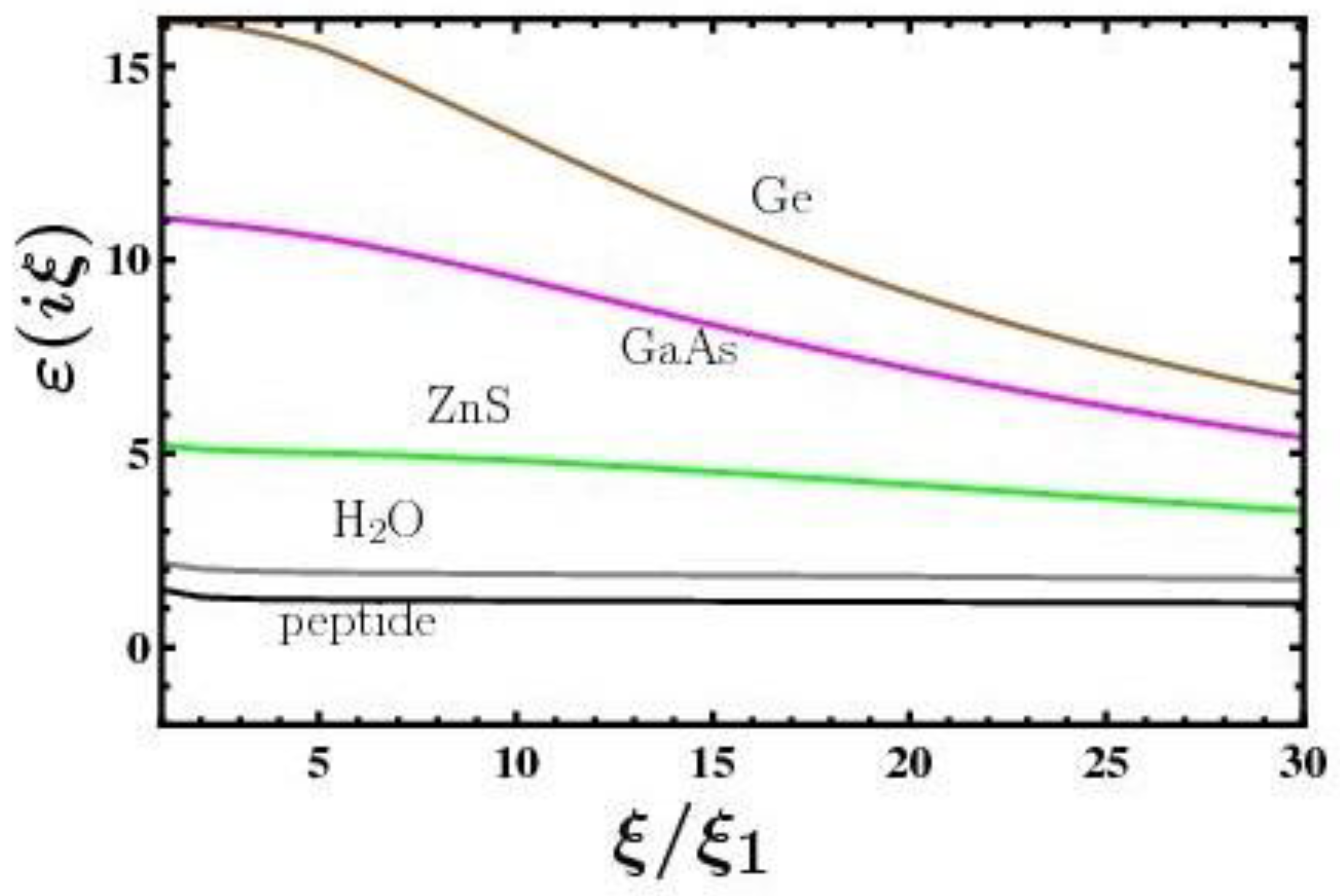
3. Dielectric Functions of Different Semiconductors and Peptide along the Imaginary Frequency Axis

We begin with the gallium arsenide. The measured optical data for the real and imaginary parts of the complex index of refraction for this semiconductor are presented in [64] over the wide frequency region from ω min = 0.00124 eV to ω max = 155 eV. Based on these data, we obtain the imaginary part of GaAs dielectric permittivity Im ε ( s ) ( ω ) = 2 Re n ( ω ) Im n ( ω ) . In the dielectric state, it is extrapolated to the frequency region 0 ω ω min by Im ε ( s ) ( ω ) = 0 . Then, the dielectric permittivity at the pure imaginary Matsubara frequencies, ε ( i ξ l ) , was computed by the standard procedure [6] using the Kramers–Kronig relation
ε ( s ) ( i ξ l ) = 1 + 2 π 0 ω Im ε ( s ) ( ω ) ω 2 + ξ l 2 d ω .
In doing so, an extrapolation of the optical data to the region of high frequencies, ω > ω max , is not needed.
In Figure 1, the obtained behavior of the dielectric permittivity of GaAs along the imaginary frequency axis is shown as the function of ξ / ξ 1 1 . The value of the static permittivity of GaAs is ε ( s ) ( 0 ) = 13.0 [64].
Next, we consider the dielectric permittivity of germanium. The optical data for Re n ( ω ) and Im n ( ω ) of Ge are also contained in [64]. They are presented in the region from ω min = 0.00248 eV to ω max = 525 eV. Using these data, the imaginary part of ε ( s ) ( ω ) was obtained in the same way as for GaAs. The dielectric permittivity of Ge at the imaginary Matsubara frequencies was found by the Kramers–Kronig relation (6).
The resulting behavior of the dielectric permittivity of Ge along the imaginary frequency axis is shown as the function of ξ / ξ 1 by the top line in Figure 1. The static permittivity of Ge in the dielectric state is ε ( s ) ( 0 ) 16.2 [64].
The last substrate semiconductor considered here is zinc sulphide. In contrast to Ge, the dielectric permittivity of ZnS with cubic crystal lattice admits sufficiently exact analytic representation along the imaginary frequency axis (the available analytic expressions for Ge are only within rather narrow intervals along the real frequency axis [65]). It is given by the contributions of ultraviolet and infrared frequencies [66]
ε ( s ) ( i ξ l ) = 1 + C IR ω IR 2 ω IR 2 + ξ l 2 + C UV ω UV 2 ω UV 2 + ξ l 2 ,
where C IR = 3.27 , C UV = 4.081 , ω IR = 5.4 × 10 13 rad/s, and ω UV = 9.39 × 10 15 rad/s. At zero Matsubara frequency, one obtains ε ( s ) ( 0 ) = 8.35 .
In Figure 1, the behavior of the dielectric permittivity of ZnS along the imaginary frequency axis is shown as the function of ξ / ξ 1 .
In the above, we considered the dielectric properties of semiconductors in the dielectric state. However, as mentioned in Section 1, at any nonzero temperature, dielectric materials are characterized by some nonzero electric conductivity σ ( ω , T ) . The contribution of this conductivity to the dielectric permittivity can be taken into account by means of the Drude-like term. In doing so, the values of dielectric permittivity of semiconductor substrate at the Matsubara frequencies with account of conductivity are given by
ε ˜ ( s ) ( i ξ l ) = ε ( s ) ( i ξ l ) + 4 π σ ( i ξ l , T ) ξ l ,
where for dielectric-type semiconductors σ ( i ξ l , T ) goes to zero exponentially fast with vanishing temperature.
In Section 1, it was also mentioned that with increasing doping concentration the semiconductors under consideration here undergo the phase transition to a metallic state. For metallic-type semiconductors, the total dielectric permittivity at the Matsubara frequencies can be again represented by (8) but with important distinctive property that the conductivity σ ( i ξ l , T ) may be by several orders of magnitude larger and it does not go to zero when the temperature vanishes.
In Section 4, we show that the account of nonzero electric conductivity of a semiconductor substrate can have a pronounced effect on the fluctuation-induced Casimir pressure in peptide coating and requires special care for reaching a physically plausible insight.
Now, we turn our attention to the dielectric permittivity of peptide film. This subject involves difficulties because there are different kinds of peptides, and for none of them the optical data were examined over a sufficiently wide frequency range. In [46], the electrically neutral 18-residue zinc finger peptide was chosen as a basic sample. The imaginary part of the dielectric permittivity of this peptide in the microwave region was investigated in [67]. It was found that ε ( p ) ( 0 ) = 15 . To estimate the dielectric properties of peptide film in the ultraviolet and infrared regions, the data computed for a cyclic tripeptide RGD-4C in [68] have been used [46] based on the fact that the films formed by this peptide and zinc finger peptide are rather similar.
As a result, the dielectric permittivity of our model peptide as the function of imaginary frequency normalized to the first Matsubara frequency is shown in Figure 1 by the bottom line in the interval ξ / ξ 1 1 .
It should be noted that peptide films usually contain some fraction of water which plays the role of a plasticizer providing the required functional properties of a film [69]. Below, we compute the Casimir pressure in peptide coatings consisting both of pure peptide with the dielectric permittivity ε ( p ) ( i ξ l ) and containing the volume fraction Φ of water. The dielectric permittivity of such films, ε Φ ( p ) ( i ξ l ) , can be found from the mixing formula suitable for the molecules of irregular shape [70]
ε Φ ( p ) ( i ξ l ) 1 ε Φ ( p ) ( i ξ l ) + 2 = Φ ε ( w ) ( i ξ l ) 1 ε ( w ) ( i ξ l ) + 2 + ( 1 Φ ) ε ( p ) ( i ξ l ) 1 ε ( p ) ( i ξ l ) + 2 ,
which follows from the Clausius–Mossotti equation.
Here, the dielectric permittivity of water at the Matsubara frequencies can be presented in the form [66]
ε ( w ) ( i ξ l ) = 1 + B 1 + τ ξ l + j = 1 11 C j ω j 2 ω j 2 + ξ l 2 + g j ξ l ,
where the second (Debye) term describes the orientation of permanent dipoles, the oscillator terms with j = 1 , 2 , , 5 correspond to the infrared region, and the oscillator terms with j = 6 , 7 , , 11 present the contribution of ultraviolet frequencies (see [46,66] for the numerical values of all parameters entering (10)).
In Figure 1, the dielectric permittivity of water computed by (10) is shown as the function of ξ / ξ 1 1 . At zero Matsubara frequency, it holds
ε ( w ) ( 0 ) = 1 + B + j = 1 11 C j 81.2 .
In the next section, the obtained information about the dielectric properties of peptide films and semiconductor substrates is used to compute the fluctuation-induced Casimir pressure.

4. Computational Results for the Casimir Pressure in Peptide Films

All the computations below were performed using the Lifshitz formula (1) at room temperature T = 300 K with the reflection coefficients (3) and (4). The semiconductor substrates in both the dielectric and metallic states are considered. We deal with the peptide films containing Φ = 0 , 10, 25, and 40% fractions of water. The computational results are presented for the GaAs, Ge, and ZnS substrates in the following subsections.

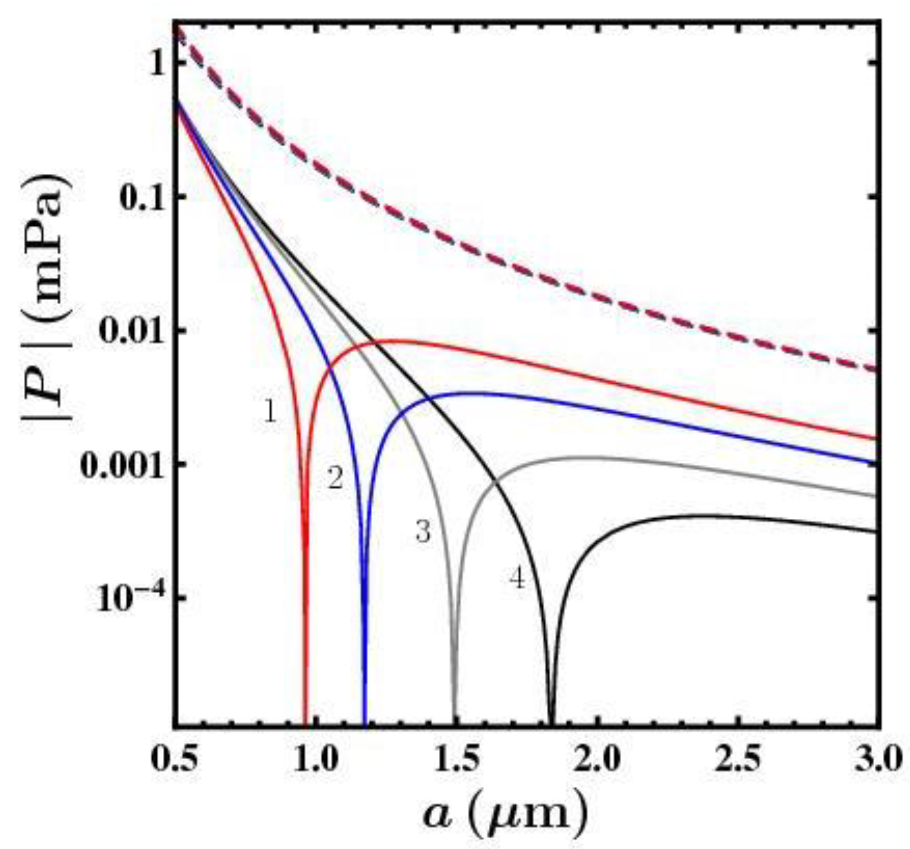
4.1. Gallium Arsenide Substrate

We computed the Casimir pressure (1) substituting there the dielectric permittivity of GaAs, ε ( s ) ( i ξ l ) , in the dielectric state shown in Figure 1, the dielectric permittivity of pure peptide, ε ( p ) ( i ξ l ) , ( Φ = 0 ), also shown in Figure 1, and the dielectric permittivities of peptide films, ε Φ ( p ) ( i ξ l ) , with Φ = 0.1 , 0.25, and 0.4 found by using (9). At ξ 0 = 0 (9) results in ε 0.1 ( p ) ( 0 ) = 16.5 , ε 0.25 ( p ) ( 0 ) = 19.2 , and ε 0.4 ( p ) ( 0 ) = 22.9 .
The magnitudes of the obtained Casimir pressures in peptide films with Φ = 0.4 , 0.25, 0.1, and 0 fractions of water on a GaAs substrate are shown in Figure 2 as the functions of the film thickness in the logarithmic scale by the lines labeled 1, 2, 3, and 4, respectively.
As is seen in Figure 2, for all four peptide films with different fractions of water the Casimir pressure turns into zero for some definite film thickness. For the films with 0.4, 0.25, 0.1, and 0 fractions of water, this happens for the film thicknesses of 0.957, 1.172, 1.492, and 1.84 μ m, respectively. For thinner films, the Casimir pressure is positive, i.e., repulsive, whereas for thicker films the pressure is negative, i.e., attractive. Depending on the relationship between the permittivities of a dielectric substrate and dielectric coating along the imaginary frequency axis, a similar effect takes place for inorganic films possessing a crystalline structure (for instance, for Al 2 O 3 coatings on a high-resistivity Si substrate) [45]. One can conclude that to be stable the peptide coating on the GaAs substrate should be sufficiently thick. According to Figure 2, for peptide films containing a smaller fraction of water, the film stability is reached for thicker films. Note that for pure water films without peptide the Casimir pressure vanishes for much smaller film thicknesses.
Now, we consider the impact of nonzero conductivity of the GaAs substrate on the Casimir pressure in a peptide film. The major contribution to this impact is given by the values of the reflection coefficient r TM ( p , s ) defined in (4) at zero Matsubara frequency. Calculating the reflection coefficients (4) at ξ 0 = 0 ignoring the electric conductivity, i.e., with the finite value of semiconductor dielectric permittivity at zero frequency ε ( s ) ( 0 ) (see in Section 3), one obtains
r TM ( p , s ) ( 0 , k ) = ε ( s ) ( 0 ) ε ( p ) ( 0 ) ε ( s ) ( 0 ) + ε ( p ) ( 0 ) , r TM ( p , s ) ( 0 , k ) = 0 .
If, however, the electric conductivity σ of a semiconductor substrate is taken into account, i.e., we calculate the reflection coefficients (4) substituting the dielectric permittivity ε ˜ ( s ) ( i ξ l ) defined in (8) in place of ε ( s ) ( i ξ l ) , the result is
r TM ( p , s ) ( 0 , k ) = 1 , r TM ( p , s ) ( 0 , k ) = 0 .
We emphasize that the difference between the values of r TM ( p , s ) ( 0 , k ) in (12) and (13) does not depend on the value of σ but only on the presence of the second term on the right-hand side of (8), i.e., it is the same whether we deal with metallic- or dielectric-type semiconductors with electric conductivity taken into account. It is also significant that when computing the Casimir pressure in a peptide coating by the Lifshitz formula (1) using either the dielectric permittivity ε ( s ) ( i ξ l ) or ε ˜ ( s ) ( i ξ l ) of the semiconductor substrate, the major difference is obtained only due to the different values of the reflection coefficient r TM ( p , s ) ( 0 , k ) in (12) and (13), whereas the contributions of all terms with l 1 are almost the same.
In Figure 2, the computational results for the Casimir pressures in the peptide films obtained with an account of the substrate conductivity by means of (8) are shown as the functions of the film thickness by the four dashed lines counted from top to bottom for the peptide films containing Φ = 0.4 , 0.25, 0.1, and 0 fractions of water, respectively. As is seen in Figure 2, the four dashed lines almost overlap. This means that when the electric conductivity of a substrate is taken into account, the fraction of water in the peptide film makes only a minor impact on the fluctuation-induced pressure.
According to the discussion presented in Section 1, for the dielectric-type GaAs substrate, the experimentally and thermodynamically consistent results for the Casimir pressure in the peptide coatings are given by the solid lines 1–4 in Figure 2. As to the GaAs substrate in a metallic state, the Casimir pressures in the peptide coatings in this case are given by the dashed lines in Figure 2.
The physical explanation for why the seemingly minor difference between the values of the reflection coefficient r TM ( p , s ) ( 0 , k ) in (12) and (13) leads to so big difference between the solid and dashed lines in Figure 2 is the following. In the configuration of a peptide film deposited on a semiconductor substrate, the contribution of all Matsubara terms with l 1 in the Lifshitz formula (1) is always positive and, thus, leads to the repulsion for both dielectric- and metallic-type semiconductors.
As to the contribution of the term with zero Matsubara frequency in (1), it is also positive for metallic-type semiconductors but may be both positive and negative (i.e., attractive) for a dielectric-type semiconductor. Really, according to (12), the sign of the reflection coefficient r TM ( p , s ) ( 0 , k ) depends on the relationship between ε ( s ) ( 0 ) and ε ( p ) ( 0 ) . For a GaAs substrate and peptide films with any fraction of water Φ from 0 to 0.4, it holds ε ( s ) ( 0 ) < ε ( p ) ( 0 ) , i.e., r TM ( p , s ) ( 0 , k ) < 0 . Taking into account that according to (3)
r TM ( p , v ) ( 0 , k ) = 1 ε ( p ) ( 0 ) 1 + ε ( p ) ( 0 ) < 0
and that at ξ 0 = 0 the TE polarization does not contribute to the Casimir pressure, one finds that the term of the Lifshitz formula (1) with l = 0 is negative, i.e., produces an attraction. Considering that with an increase in film thickness the relative role of the zero-frequency term in the total pressure increases, this leads to the change of repulsion with attraction as is demonstrated by the solid lines in Figure 2. Another situation is illustrated by the Ge substrate and peptide film which does not contain water (see below).

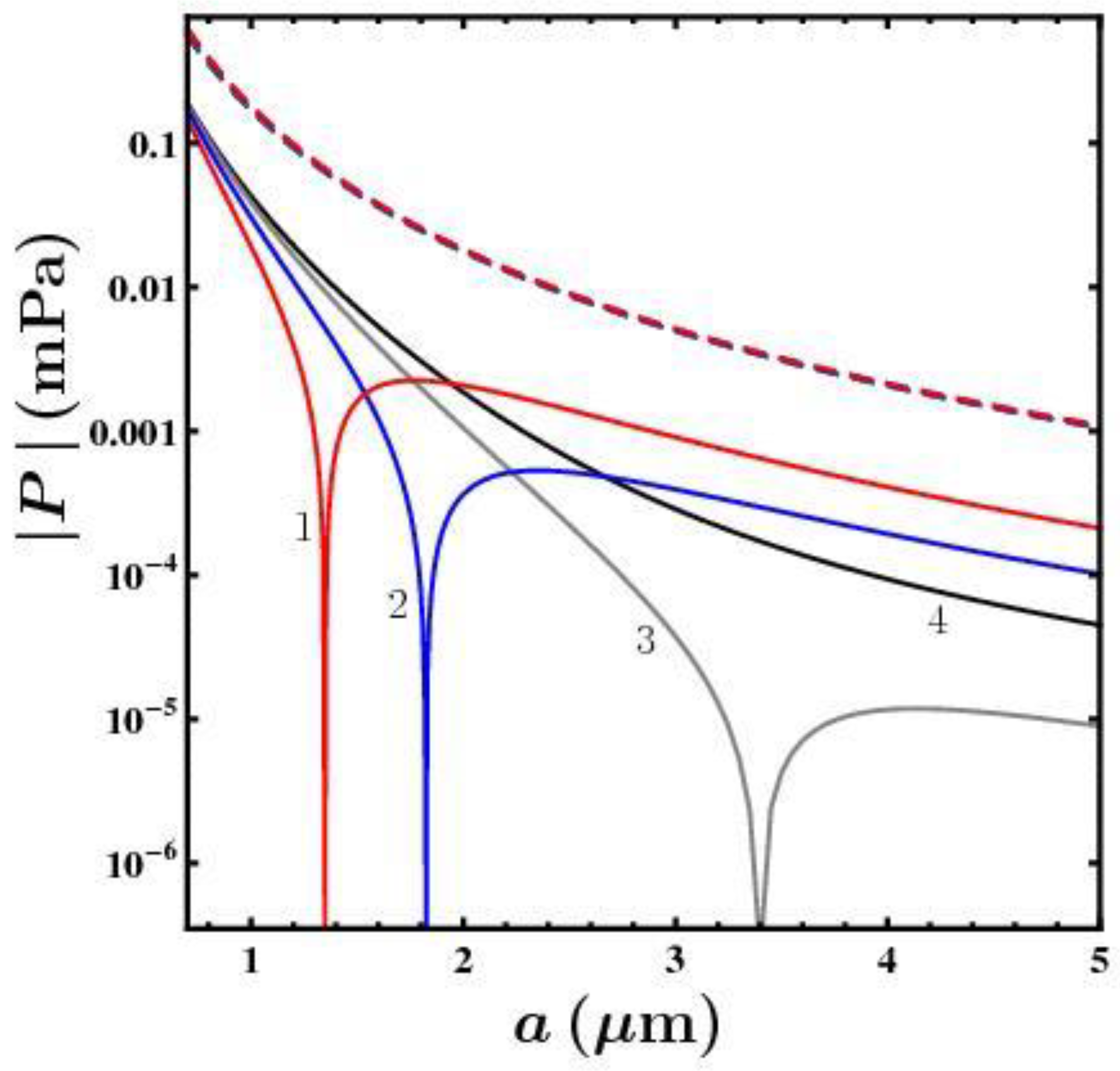
4.2. Germanium Substrate

For peptide films deposited on a Ge substrate in the dielectric state, the computations of the Casimir pressure were performed in the same way as described above for the case of the GaAs substrate. In doing so, the dielectric permittivity of Ge along the imaginary frequency axis was used (see the top line in Figure 1).
In Figure 3, the computational results for the peptide films with Φ = 0.4 , 0.25, 0.1, and 0 fractions of water deposited on a Ge substrate are shown as the functions of the film thickness in the logarithmic scale by the solid lines labeled 1, 2, 3, and 4, respectively.
From Figure 3, it is seen that for a Ge substrate in the dielectric state the Casimir pressure in peptide films containing Φ = 0.4 , 0.25, and 0.1 fractions of water turns into zero for the film thicknesses equal to 1.349, 1.824, and 3.359 μ m, respectively. For thinner films, the fluctuation-induced pressure in the film is repulsive, whereas for thicker films it is attractive, making the film more stable.
The change in the pressure sign is explained in the same way as was considered in Section 4.1 in the case of the GaAs substrate. Thus, for the peptide films containing nonzero fractions of water Φ under consideration here, it holds ε ( s ) ( 0 ) = 16.2 < ε Φ ( p ) ( 0 ) . As a result, the zero-frequency term in the Lifshitz formula is negative, i.e., contributes to the attraction. With an increasing film thickness, the relative role of this term in the total pressure increases. Because of this, for sufficiently thick films, the total Casimir pressure becomes attractive.
An alternative situation takes place for a pure peptide film ( Φ = 0 ) deposited on a Ge substrate. In this case, ε ( s ) ( 0 ) = 16.2 > ε ( p ) ( 0 ) = 15.0. As a result, the reflection coefficient r ( p , s ) ( 0 , k ) in (12) becomes positive. Taking into account (14), this leads to the positive zero-frequency contribution to the Lifshitz formula (1), i.e., the Casimir pressure in the pure peptide film deposited on a Ge substrate remains repulsive for films of any thickness. This is illustrated by the solid line labeled 4 in Figure 3.
For the metallic-type Ge substrate described by the dielectric permittivity (8), the Casimir pressure in peptide films with any fraction of water is repulsive. In this case, the computational results are shown by the dashed lines in Figure 3 which almost overlap for different fractions of water Φ in a film. Here, the difference in the values of the Casimir pressure with the case of a GaAs substrate shown in Figure 2 is only quantitative.

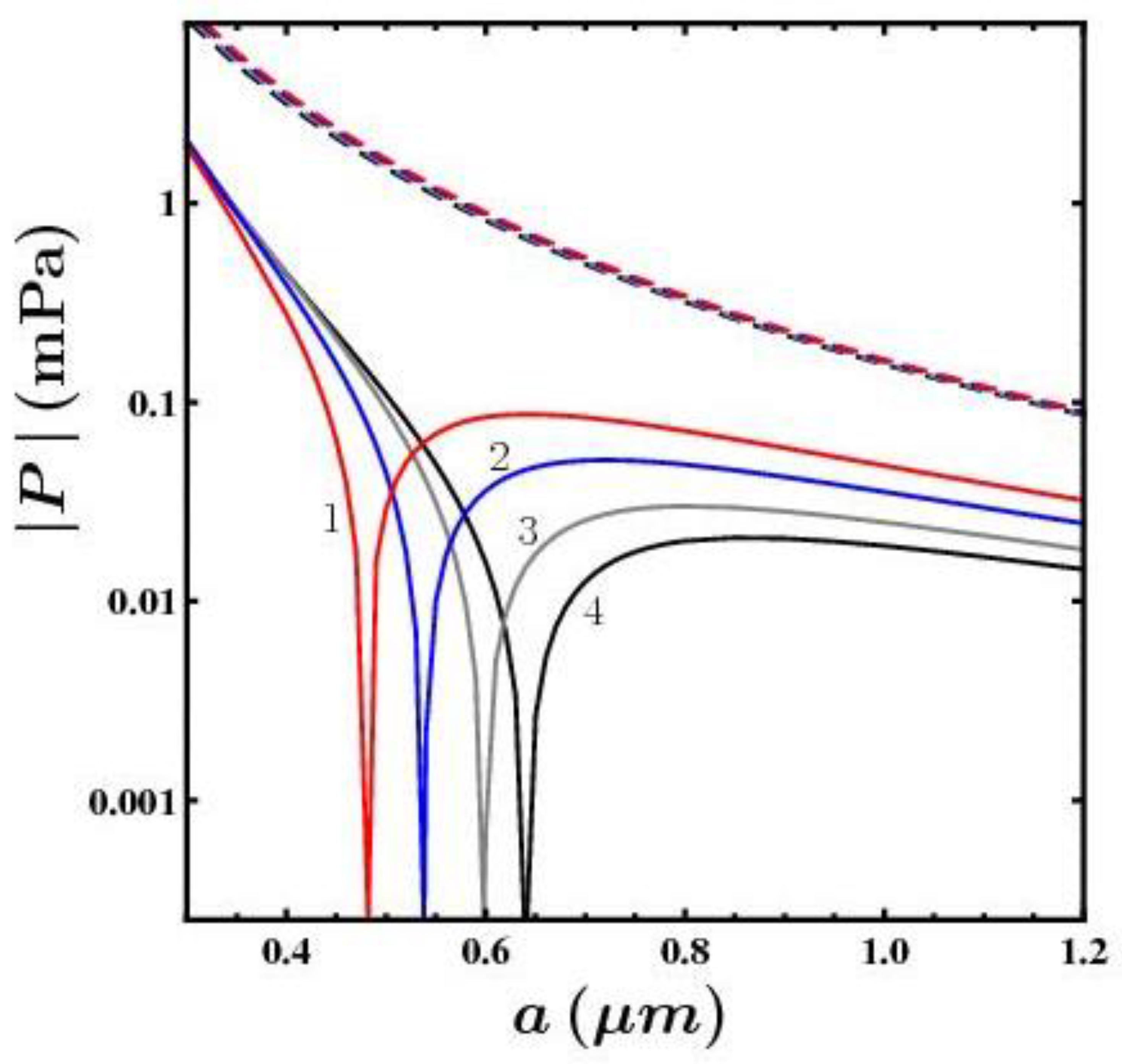
4.3. Zinc Sulfide Substrate

The Casimir pressure in peptide films deposited on a ZnS substrate is typically characterized by the same behavior as for the case of the GaAs substrate, but the change from repulsive to attractive forces takes place for thinner films. All computations are performed by the Lifshitz formula (1) as described above. However, for the dielectric permittivity of ZnS at the Matsubara frequencies, in place of the optical data [64] and dispersion relation (6), it is now possible to employ the analytic representation (7).
The computational results for the Casimir pressure in peptide films with Φ = 0.4 , 0.25, 0.1, and 0 fractions of water deposited on a ZnS substrate in the dielectric state are shown in Figure 4 as the functions of the film thickness in the logarithmic scale by the four solid lines labeled 1, 2, 3, and 4, respectively.
As is seen in Figure 4, for the films containing Φ = 0.4 , 0.25, 0.1, and 0 fractions of water, the Casimir pressure vanishes for the film thicknesses of 0.479, 0.537, 0.598, and 0.642 μ m, respectively. Similar to the cases of the GaAs and Ge substrates, the Casimir pressures for thinner films are repulsive and for thicker films—attractive. The latter makes the peptide coatings more stable. In an analogy to the other substrate semiconductors considered above, for peptide films containing less water, the Casimir pressure changes its sign for thicker films. The eventual reason why for the ZnS substrate the change in the sign of the pressure in the film containing some fixed fraction of water occurs for smaller film thickness than for GaAs and Ge substrates is that the static dielectric permittivity of ZnS, ϵ ( s ) ( 0 ) = 8.35 , is smaller than for GaAs and Ge (13.0 and 16.2, respectively).
For a ZnS substrate in the metallic state, the dielectric permittivity at the pure imaginary Matsubara frequencies is given by (8) where ϵ ( s ) ( i ξ l ) is again expressed by (7). In this case, the Casimir pressures in peptide films containing Φ = 0.4, 0.25, 0.1, and 0 fractions of water are presented in Figure 4 by the four dashed lines counted from top to bottom, respectively. By comparing the dashed lines in Figure 2, Figure 3 and Figure 4, one can conclude that decreasing the static dielectric permittivity of a semiconductor substrate results in an increased impact of the fraction of water in the film on the fluctuation-induced pressure.

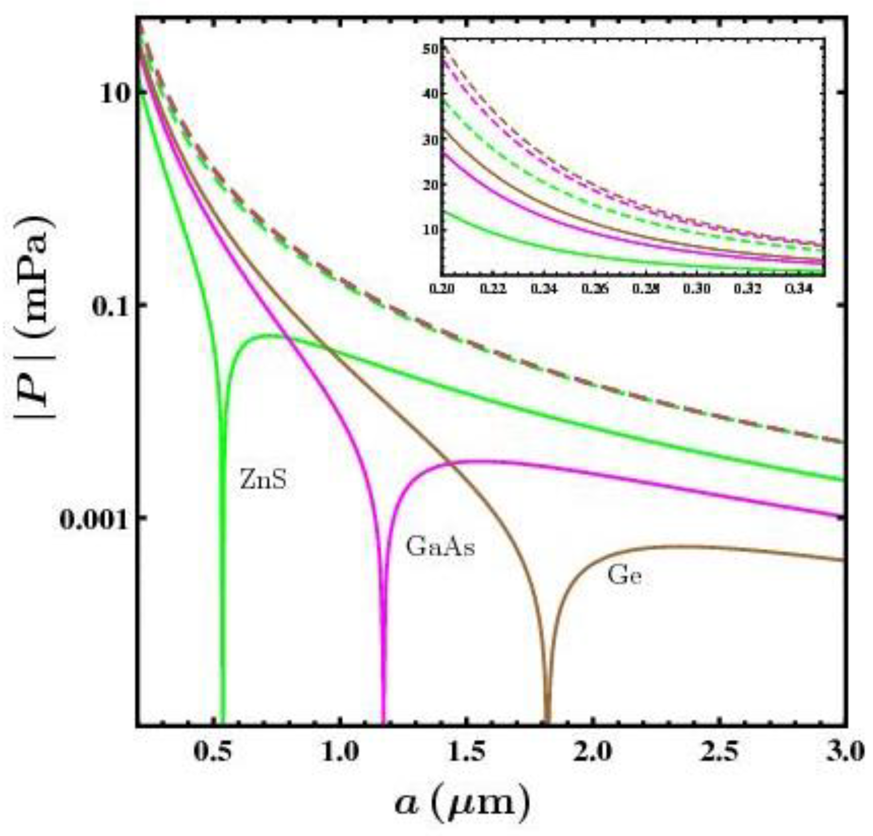
4.4. Comparison between Different Substrates

To illustrate in a more illuminative manner the difference in the fluctuation-induced pressures in some fixed peptide film deposited on different semiconductor substrates, we consider the film containing the 25% fraction of water. In Figure 5, the magnitudes of the Casimir pressure in this film deposited on the ZnS, GaAs, and Ge substrates in the dielectric state are shown by the solid lines as the functions of the film thickness. The three dashed lines counted from top to bottom present the Casimir pressure in the same peptide film deposited on the Ge, GaAs, and ZnS substrates in the metallic state, respectively. In the inset, the region of small film thicknesses is shown on an enlarged scale, allowing clear discrimination among the dashed lines.
For the dielectric-type semiconductors, the Casimir pressure in the peptide film vanishes for the film thicknesses of 0.537, 1.172, and 1.824 μ m for the ZnS, GaAs, and Ge substrates, respectively. This is in agreement with Figure 2, Figure 3 and Figure 4 and illustrates the dependence of the pressure roots on the static dielectric permittivity of the semiconductor materials mentioned above.
In the case of metallic-type semiconductor substrates, a disposition of the dashed lines in the inset to Figure 5 can also be connected with a relationship between the static dielectric permittivities of these substrates. Thus, the top dashed line and that one below it are rather close. They are for the Ge and GaAs substrates with ϵ ( s ) = 16.2 and 13.0, respectively. As to the bottom dashed line related to a ZnS substrate, it is more distant from the first two in agreement with a much lower value of the static permittivity of ZnS, ϵ ( s ) ( 0 ) = 8.35 .

5. Discussion

In this paper, we have considered the fluctuation-induced pressure in peptide films deposited on substrates made of widely employed semiconductors of GaAs, Ge, and ZnS. The dielectric permittivities for peptide films containing different fractions of water at the Matsubara frequencies found in the previous literature were used in the computations. The fluctuation-induced (Casimir) pressure in peptide films was investigated in the framework of the fundamental Lifshitz theory for both dielectric- and metallic-type semiconductor substrates. The dielectric properties of these substrates were determined using the available optical data for the complex indices of refraction of GaAs and Ge and the analytic representation for ZnS. The electric conductivity of substrates was omitted for the dielectric-type semiconductors and included for semiconductors in the metallic state, i.e., using the experimentally and thermodynamically consistent approach to the Lifshitz theory [6,45,49,53,54,55,56,57,59,60,61,62].
According to the results obtained, the Casimir pressure in peptide films deposited on dielectric-type semiconductor substrates is repulsive for sufficiently thin films, vanishes for the films of definite thickness, and becomes attractive for thicker films in most cases. The value of the film thickness, which ensures the null Casimir pressure, increases with a decreasing fraction of water in the film and with an increasing static dielectric permittivity of substrate materials. For the metallic-type semiconductor substrates, the Casimir pressure in peptide coatings is always repulsive. It decreases with a decreasing fraction of water in the film and with a decreasing static dielectric permittivity of a semiconductor substrate defined in the dielectric state.

6. Conclusions

Peptide films do not possess the crystal structure, and their properties are significantly different from the properties of metallic and dielectric ones. They consist of big asymmetric molecules and their dielectric permittivities are not yet investigated over sufficiently wide frequency regions.
Taking into account that peptide coatings are used in organic electronics, the problem of their stability with a further decrease in the characteristic sizes of microdevices and film thicknesses may become important not only for fundamental science but also for its technological applications. The obtained results can be used as an indication of the ranges of film and substrate parameters which lead to the attractive Casimir pressure in the film and, thus, are favorable for its stability.

Author Contributions

Conceptualization, G.L.K., V.M.M. and O.Y.T.; investigation, G.L.K. and V.M.M.; writing—original draft, V.M.M.; writing—review and editing, G.L.K. and O.Y.T. All authors have read and agreed to the published version of the manuscript.

Funding

The work of O.Y.T. was supported by the Russian Science Foundation under Grant No. 21-72-20029. G.L.K. and V.M.M. were partially supported by the Peter the Great Saint Petersburg Polytechnic University in the framework of the Russian state assignment for basic research (Project No. FSEG-2020-0024). The work of V.M.M. was also supported by the Kazan Federal University Strategic Academic Leadership Program.

Institutional Review Board Statement

Not applicable.

Informed Consent Statement

Not applicable.

Data Availability Statement

Not applicable.

Conflicts of Interest

The authors declare no conflict of interest.

References

  1. Mahanty, J.; Ninham, B.W. Dispersion Forces; Academic Press: London, UK, 1976. [Google Scholar]
  2. Milton, K.A. The Casimir Effect: Physical Manifestations of Zero-Point Energy; World Scientific: Singapore, 2001. [Google Scholar]
  3. Parsegian, V.A. Van der Waals Forces: A Handbook for Biologists, Chemists, Engineers, and Physicists; Cambridge University Press: Cambridge, UK, 2005. [Google Scholar]
  4. Israelachvili, J. Intermolecular and Surface Forces; Academic Press: San Diego, CA, USA, 1992. [Google Scholar]
  5. Buhmann, S.Y. Disperson Forces; Springer: Berlin, Germany, 2012; Volumes 1 and 2. [Google Scholar]
  6. Bordag, M.; Klimchitskaya, G.L.; Mohideen, U.; Mostepanenko, V.M. Advances in the Casimir Effect; Oxford University Press: Oxford, UK, 2015. [Google Scholar]
  7. Sernelius, B.E. Fundamentals of van der Waals and Casimir Interactions; Springer: New York, NY, USA, 2018. [Google Scholar]
  8. Chan, H.B.; Aksyuk, V.A.; Kleiman, R.N.; Bishop, D.J.; Capasso, F. Quantum mechanical actuation of microelectromechanical system by the Casimir effect. Science 2001, 291, 1941–1944. [Google Scholar] [CrossRef] [PubMed] [Green Version]
  9. Chan, H.B.; Aksyuk, V.A.; Kleiman, R.N.; Bishop, D.J.; Capasso, F. Nonlinear Micromechanical Casimir Oscillator. Phys. Rev. Lett. 2001, 87, 211801. [Google Scholar] [CrossRef] [PubMed] [Green Version]
  10. Buks, E.; Roukes, M.L. Stiction, adhesion, and the Casimir effect in micromechanical systems. Phys. Rev. B 2001, 63, 033402. [Google Scholar] [CrossRef] [Green Version]
  11. Buks, E.; Roukes, M.L. Metastability and the Casimir effect in micromechanical systems. Europhys. Lett. 2001, 54, 220–226. [Google Scholar] [CrossRef] [Green Version]
  12. Barcenas, J.; Reyes, L.; Esquivel-Sirvent, R. Scaling of micro- and nanodevices actuated by the Casimir force. Appl. Phys. Lett. 2005, 87, 263106. [Google Scholar] [CrossRef]
  13. Palasantzas, G. Contact angle influence on the pull-in voltage of microswitches in the presence of capillary and quantum vacuum effects. J. Appl. Phys. 2007, 101, 053512. [Google Scholar] [CrossRef] [Green Version]
  14. Palasantzas, G. Pull-in voltage of microswitch rough plates in the presence of electromagnetic and acoustic Casimir forces. J. Appl. Phys. 2007, 101, 063548. [Google Scholar] [CrossRef] [Green Version]
  15. Esquivel-Sirvent, R.; Pérez-Pascual, R. Geometry and charge carrier induced stability in Casimir actuated nanodevices. Eur. Phys. J. B 2013, 86, 467. [Google Scholar] [CrossRef]
  16. Broer, W.; Palasantzas, G.; Knoester, G.; Svetovoy, V.B. Significance of the Casimir force and surface roughness for actuation dynamics of MEMS. Phys. Rev. B 2013, 87, 125413. [Google Scholar] [CrossRef] [Green Version]
  17. Sedighi, M.; Broer, W.; Palasantzas, G.; Kooi, B.J. Sensitivity of micromechanical actuation on amorphous to crystalline phase transformations under the influence of Casimir forces. Phys. Rev. B 2013, 88, 165423. [Google Scholar] [CrossRef]
  18. Zou, J.; Marcet, Z.; Rodriguez, A.W.; Reid, M.T.H.; McCauley, A.P.; Kravchenko, I.I.; Lu, T.; Bao, Y.; Johnson, S.G.; Chan, H.B. Casimir forces on a silicon micromechanical chip. Nat. Commun. 2013, 4, 1845. [Google Scholar] [CrossRef] [PubMed] [Green Version]
  19. Broer, W.; Waalkens, H.; Svetovoy, V.B.; Knoester, J.; Palasantzas, G. Nonlinear Actuation Dynamics of Driven Casimir Oscillators with Rough Surfaces. Phys. Rev. Appl. 2013, 4, 054016. [Google Scholar] [CrossRef] [Green Version]
  20. Liu, X.-F.; Li, Y.; Jing, H. Casimir switch: Steering optical transparancy with vacuum forces. Sci. Rep. 2016, 6, 27102. [Google Scholar] [CrossRef] [PubMed]
  21. Tang, L.; Wang, M.; Ng, C.Y.; Nicolic, M.; Chan, C.T.; Rodriguez, A.W.; Chan, H.B. Measurement of nonmonotonic Casimir forces between silicon nanostructures. Nat. Photonics 2017, 11, 97. [Google Scholar] [CrossRef] [Green Version]
  22. Inui, N. Optical switching of a graphene mechanical switch using the Casimir effect. J. Appl. Phys. 2017, 122, 104501. [Google Scholar] [CrossRef]
  23. Klimchitskaya, G.L.; Mostepanenko, V.M.; Petrov, V.M.; Tschudi, T. Demonstration of the Optical Chopper Driven by the Casimir Force. Phys. Rev. Appl. 2018, 10, 014010. [Google Scholar] [CrossRef] [Green Version]
  24. Sharma, S.; Johnson, R.W.; Desai, T.A. Evaluation of the stability of nonfouling ultrathin poly(elhylene glucol) films for silicon-based microdevices. Langmuir 2004, 20, 348–356. [Google Scholar] [CrossRef]
  25. Natesan, M.; Ulrich, R.G. Protein microarrays, and biomarkers of infection disease. Int. J. Mol. Sci. 2010, 11, 5165–5183. [Google Scholar] [CrossRef] [Green Version]
  26. Chandra, H.; Reddy, P.J.; Srivastava, S. Protein microarrays and novel detection platforms. Expert Rev. Proteom. 2011, 8, 61–79. [Google Scholar] [CrossRef]
  27. Panda, S.S.; Katz, H.E.; Tovar, J.D. Solid-state electrical applications of protein and peptide based nanomaterials. Chem. Soc. Rev. 2018, 47, 3640–3658. [Google Scholar] [CrossRef]
  28. Lee, P.M.; Xiong, Z.; Ho, J. Methods for powering bioelectronic microdevices. Bioelectron. Med. 2018, 1, 201–217. [Google Scholar] [CrossRef] [Green Version]
  29. Dyubo, D.; Tsybin, O.Y. Computer Simulation of a Surface Charge Nanobiosensor with Internal Signal Integration. Biosensors 2021, 11, 397. [Google Scholar] [CrossRef] [PubMed]
  30. Baranov, M.A.; Tsybin, O.Y.; Velichko, E.N. Structured biomolecular films for microelectronics. St. Petersburg Polytechnic Univ. J. Phys. Math. 2021, 14, 85–99. [Google Scholar]
  31. Lifshitz, E.M. The theory of molecular attractive forces between solids. Zh. Eksp. Teor. Fiz. 1955, 29, 94–110, Translated: Sov. Phys. JETP 1956, 2, 73–83. [Google Scholar]
  32. Lifshitz, E.M.; Pitaevskii, L.P. Statistical Physics; Pt II; Pergamon: Oxford, UK, 1980. [Google Scholar]
  33. Emig, T.; Graham, N.; Jaffe, R.L.; Kardar, M. Casimir Forces between Arbitrary Compact Objects. Phys. Rev. Lett. 2007, 99, 170403. [Google Scholar] [CrossRef] [Green Version]
  34. Kenneth, O.; Klich, I. Casimir forces in a T-operator approach. Phys. Rev. B 2008, 78, 014103. [Google Scholar] [CrossRef] [Green Version]
  35. Rahi, S.J.; Emig, T.; Graham, N.; Jaffe, R.L.; Kardar, M. Scattering theory approach to electrodynamic Casimir forces. Phys. Rev. D 2009, 80, 085021. [Google Scholar] [CrossRef] [Green Version]
  36. Parsegian, V.A.; Ninham, B.W. Application of the Lifshitz theory to the calculation of van der Waals forces across thin lipid films. Nature 1969, 224, 1197–1198. [Google Scholar] [CrossRef]
  37. Nir, S. Van der Waals interactions between surfaces of biological interest. Prog. Surf. Sci. 1977, 8, 1–58. [Google Scholar] [CrossRef]
  38. Roth, C.M.; Neal, B.L.; Lenhoff, A.M. Van der Waals interactions involving proteins. Biophys. J. 1996, 70, 977–987. [Google Scholar] [CrossRef] [Green Version]
  39. Lu, B.-S.; Podgornik, R. Effective interactions between fluid membranes. Phys. Rev. E 2015, 92, 022112. [Google Scholar] [CrossRef] [PubMed] [Green Version]
  40. Klimchitskaya, G.L.; Mostepanenko, V.M. Casimir free energy of metallic films: Discriminating between Drude and plasma model approaches. Phys. Rev. A 2015, 92, 042109. [Google Scholar] [CrossRef]
  41. Klimchitskaya, G.L.; Mostepanenko, V.M. Casimir and van der Waals energy of anisotropic atomically thin metallic films. Phys. Rev. B 2015, 92, 205410. [Google Scholar] [CrossRef] [Green Version]
  42. Klimchitskaya, G.L.; Mostepanenko, V.M. Casimir free energy and pressure for magnetic metal films. Phys. Rev. B 2016, 94, 045404. [Google Scholar] [CrossRef] [Green Version]
  43. Klimchitskaya, G.L.; Mostepanenko, V.M. Characteristic properties of the Casimir free energy for metal films deposited on metallic plates. Phys. Rev. A 2016, 93, 042508. [Google Scholar] [CrossRef] [Green Version]
  44. Klimchitskaya, G.L.; Mostepanenko, V.M. Low-temperature behavior of the Casimir free energy and entropy of metallic films. Phys. Rev. A 2017, 95, 012130. [Google Scholar] [CrossRef] [Green Version]
  45. Klimchitskaya, G.L.; Mostepanenko, V.M. Casimir free energy of dielectric films: Classical limit, low-temperature behavior and control. J. Phys. Condens. Matter 2016, 29, 275701. [Google Scholar] [CrossRef] [Green Version]
  46. Baranov, M.A.; Klimchitskaya, G.L.; Mostepanenko, V.M.; Velichko, E.N. Fluctuation-induced free energy of thin peptide films. Phys. Rev. E 2019, 99, 022410. [Google Scholar] [CrossRef] [Green Version]
  47. Velichko, E.N.; Baranov, M.A.; Mostepanenko, V.M. Change of sign in the Casimir interaction of peptide films deposited on a dielectric substrate. Mod. Phys. Lett. A 2020, 35, 2040020. [Google Scholar] [CrossRef]
  48. Klimchitskaya, G.L.; Mostepanenko, V.M.; Velichko, E.N. Effect of increased stability of peptide-based coatings in the Casimir regime via nanoparticle doping. Phys. Rev. B 2020, 102, 161405. [Google Scholar] [CrossRef]
  49. Klimchitskaya, G.L.; Mohideen, U.; Mostepanenko, V.M. The Casimir force between real materials: Experiment and theory. Rev. Mod. Phys. 2009, 81, 1827–1885. [Google Scholar] [CrossRef] [Green Version]
  50. Klimchitskaya, G.L.; Mohideen, U.; Mostepanenko, V.M. How to modify the van der Waals and Casimir forces without change of the dielectric permittivity. J. Phys. Condens. Matter 2012, 24, 424202. [Google Scholar] [CrossRef] [PubMed]
  51. Woods, L.M.; Dalvit, D.A.R.; Tkatchenko, A.; Rodriguez-Lopez, P.; Rodriguez, A.W.; Podgornik, R. Materials perspective on Casimir and van der Waals interactions. Rev. Mod. Phys. 2016, 88, 045003. [Google Scholar] [CrossRef] [Green Version]
  52. Mostepanenko, V.M. Casimir Puzzle and Conundrum: Discovery and Search for Resolution. Universe 2021, 7, 84. [Google Scholar] [CrossRef]
  53. Chen, F.; Klimchitskaya, G.L.; Mostepanenko, V.M.; Mohideen, U. Demonstration of optically modulated dispersion forces. Opt. Express 2007, 15, 4823–4829. [Google Scholar] [CrossRef] [PubMed] [Green Version]
  54. Chen, F.; Klimchitskaya, G.L.; Mostepanenko, V.M.; Mohideen, U. Control of the Casimir force by the modification of dielectric properties with light. Phys. Rev. B 2007, 76, 035338. [Google Scholar] [CrossRef] [Green Version]
  55. Klimchitskaya, G.L.; Mostepanenko, V.M. Conductivity of dielectric and thermal atom-wall interaction. J. Phys. A Math. Theor. 2008, 41, 312002. [Google Scholar] [CrossRef] [Green Version]
  56. Chang, C.-C.; Banishev, A.A.; Klimchitskaya, G.L.; Mostepanenko, V.M.; Mohideen, U. Reduction of the Casimir Force from Indium Tin Oxide Film by UV Treatment. Phys. Rev. Lett. 2011, 107, 090403. [Google Scholar] [CrossRef] [Green Version]
  57. Banishev, A.A.; Chang, C.-C.; Castillo-Garza, R.; Klimchitskaya, G.L.; Mostepanenko, V.M.; Mohideen, U. Modifying the Casimir force between indium tin oxide film and Au sphere. Phys. Rev. B 2012, 85, 045436. [Google Scholar] [CrossRef] [Green Version]
  58. Mostepanenko, V.M. How to confirm and exclude different models of material properties in the Casimir effect. J. Phys. Condens. Matter 2015, 27, 214013. [Google Scholar] [CrossRef] [Green Version]
  59. Obrecht, J.M.; Wild, R.J.; Antezza, M.; Pitaevskii, L.P.; Stringari, S.; Cornell, E.A. Measurement of the temperature dependence of the Casimir-Polder force. Phys. Rev. Lett. 2007, 98, 063201. [Google Scholar] [CrossRef] [PubMed] [Green Version]
  60. Geyer, B.; Klimchitskaya, G.L.; Mostepanenko, V.M. Thermal quantum field theory and the Casimir interaction between dielectrics. Phys. Rev. D 2005, 72, 085009. [Google Scholar] [CrossRef]
  61. Klimchitskaya, G.L.; Mohideen, U.; Mostepanenko, V.M. Casimir-Polder force between an atom and a dielectric plate: Thermodynamics and experiment. J. Phys. A Math. Theor. 2008, 41, 432001. [Google Scholar] [CrossRef] [Green Version]
  62. Klimchitskaya, G.L.; Korikov, C.C. Casimir entropy for magnetodielectrics. J. Phys. Condens. Matter 2015, 27, 214007. [Google Scholar] [CrossRef] [PubMed]
  63. Klimchitskaya, G.L.; Mostepanenko, V.M. Observability of thermal effects in the Casimir interaction with graphene-coated substrates. Phys. Rev. A 2014, 89, 052512. [Google Scholar] [CrossRef] [Green Version]
  64. Palik, E.D. (Ed.) Handbook of Optical Constants of Solids; Academic Press: New York, NY, USA, 1985. [Google Scholar]
  65. Barnes, N.P.; Piltch, M.S. Temperature-dependent Sellmeier coefficients and nonlinear optics average power limits for germanium. J. Opt. Soc. Am. 1979, 69, 178–180. [Google Scholar] [CrossRef]
  66. Bergström, L. Hamaker constant of inorganic materials. Adv. Coll. Interface Sci. 1979, 70, 125–169. [Google Scholar] [CrossRef]
  67. Löffler, G.; Schreiber, H.; Steinhauser, O. Calculation of the Dielectric Properties of a Protein and its Solvent: Theory and a Case Study. J. Mol. Biol. 1997, 270, 520–534. [Google Scholar] [CrossRef] [Green Version]
  68. Adhikari, P.; Wen, A.M.; French, R.H.; Parsegian, V.A.; Steinmetz, N.F.; Podgornik, R.; Ching, W.-Y. Electronic Structure, Dielectric Response, and Surface Charge Distribution of RGD (1FUV) Peptide. Sci. Rep. 2014, 4, 5605. [Google Scholar] [CrossRef] [Green Version]
  69. Krochta, J.M. Proteins as Raw Materials for Films and Coatings: Definitions, Current Status, and Opportunities. In Protein-Based Films and Coatings; Gennadios, A., Ed.; CRC Press: Boca Raton, FL, USA, 2002; p. 1. [Google Scholar]
  70. Hough, D.B.; White, L.H. The calculation of Hamaker constant from Lifshitz theory with application to wetting phenomena. Adv. Coll. Interface Sci. 1980, 14, 3–41. [Google Scholar] [CrossRef]
Figure 1. The dielectric permittivities of germanium, gallium arsenide, zinc sulphide, water, and pure peptide along the imaginary frequency axis are shown as the functions of imaginary frequency normalized to the first Matsubara frequency in the region ξ > ξ 1 .
Symmetry 14 02196 g001
Figure 2. The magnitudes of the Casimir pressure in peptide films containing Φ = 0.4, 0.25, 0.1, and 0 fractions of water deposited on a GaAs substrate in the dielectric state are shown as the functions of film thickness by the solid lines labeled 1, 2, 3, and 4, respectively. For a GaAs substrate in the metallic state, the pressure magnitudes in the same peptide films are shown by the dashed lines (see the text for further discussion).
Symmetry 14 02196 g002
Figure 3. The magnitudes of the Casimir pressure in peptide films containing Φ = 0.4, 0.25, 0.1, and 0 fractions of water deposited on a Ge substrate in the dielectric state are shown as the functions of film thickness by the solid lines labeled 1, 2, 3, and 4, respectively. For a Ge substrate in the metallic state, the pressure magnitudes in the same peptide films are shown by the overlapping dashed lines.
Symmetry 14 02196 g003
Figure 4. The magnitudes of the Casimir pressure in peptide films containing Φ = 0.4, 0.25, 0.1, and 0 fractions of water deposited on a ZnS substrate in the dielectric state are shown as the functions of film thickness by the solid lines labeled 1, 2, 3, and 4, respectively. For a ZnS substrate in the metallic state, the pressure magnitudes in the same peptide films are shown by the dashed lines (see the text for further discussion).
Symmetry 14 02196 g004
Figure 5. The magnitudes of the Casimir pressure in peptide film containing Φ = 0.25 fraction of water deposited on ZnS, GaAs, and Ge substrates in the dielectric state are shown as the functions of film thickness by the solid lines. For the semiconductors in metallic state, the pressure magnitudes are shown by the three dashed lines counted from top to bottom for Ge, GaAs, and ZnS substrates, respectively. The region of small film thicknesses is shown in the inset on an enlarged scale.
Symmetry 14 02196 g005
Publisher’s Note: MDPI stays neutral with regard to jurisdictional claims in published maps and institutional affiliations.

