

Recent Advances in Multi-Material 3D Printing of Functional Ceramic Devices


Abstract
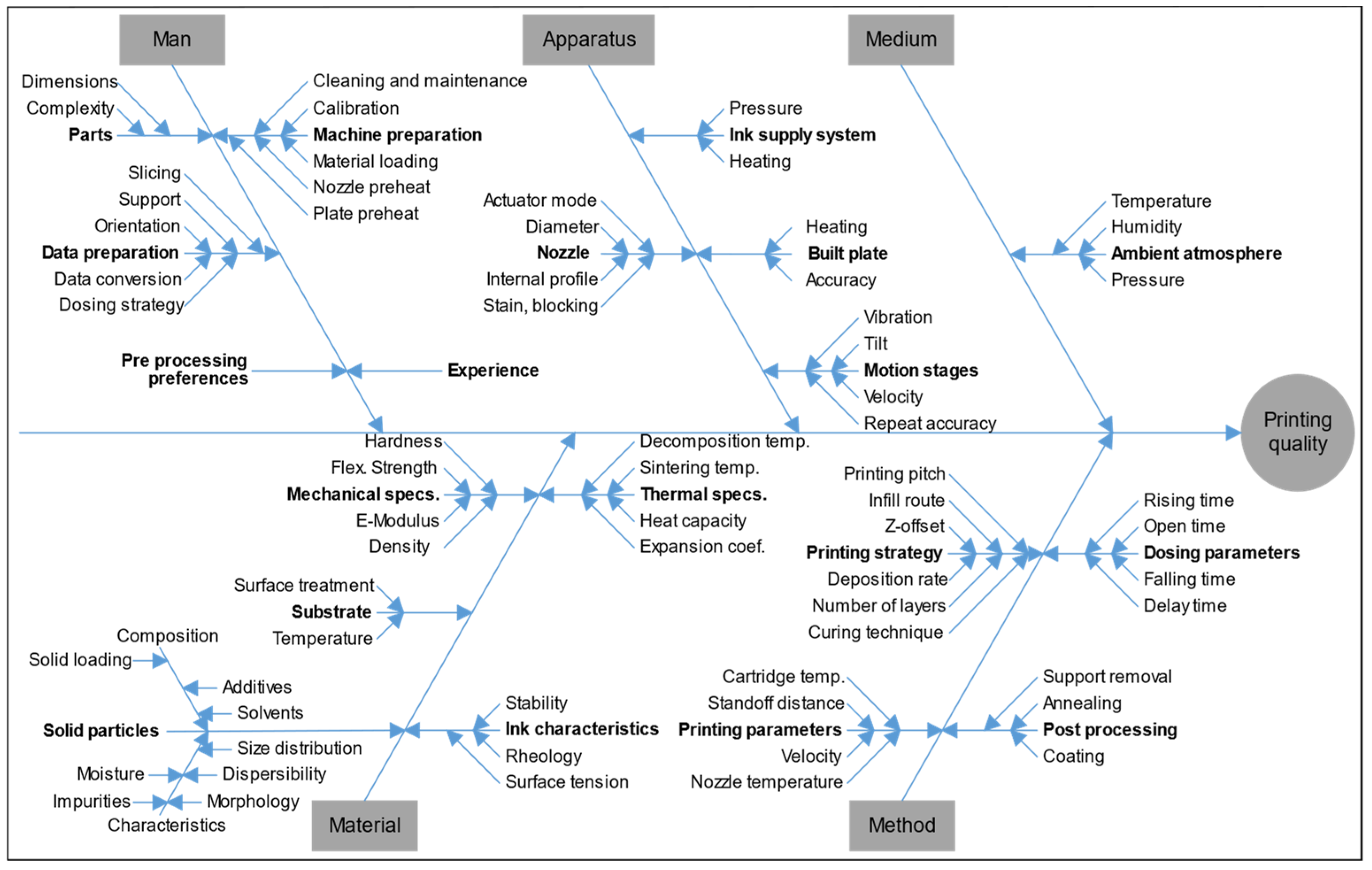
:1. Introduction
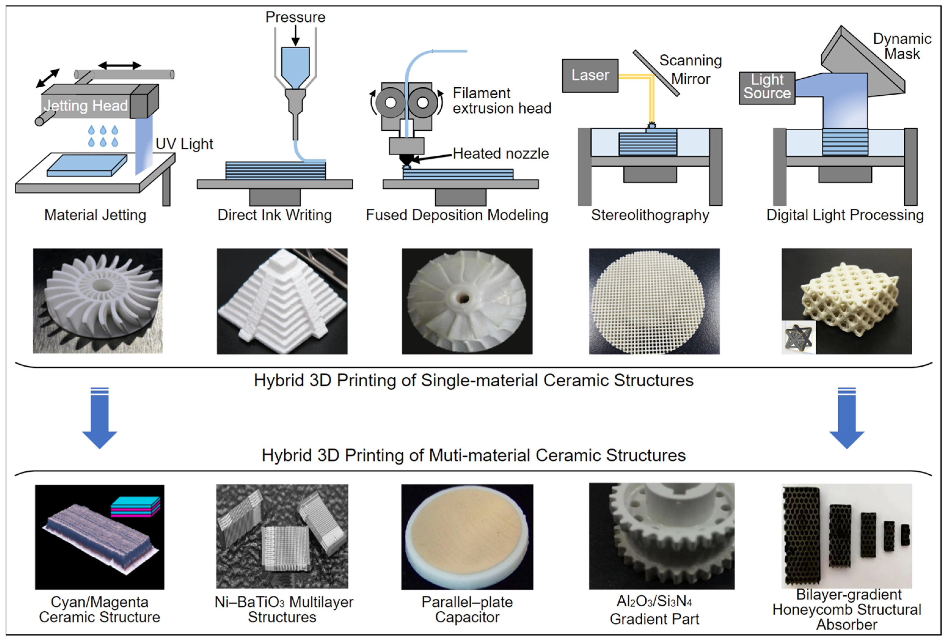
2. Multi-Material 3D Printing Methods
2.1. Material Jetting (MJ)
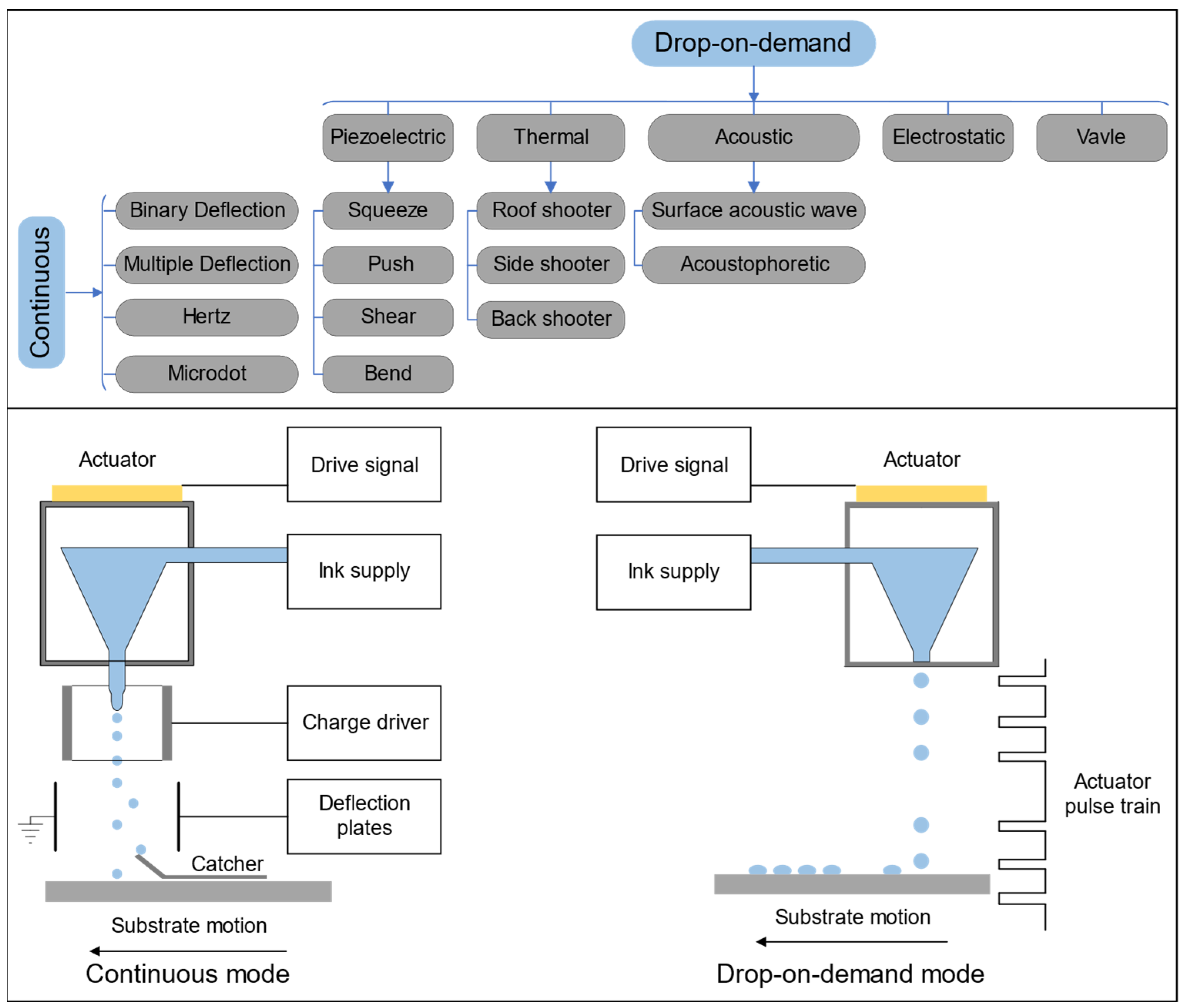
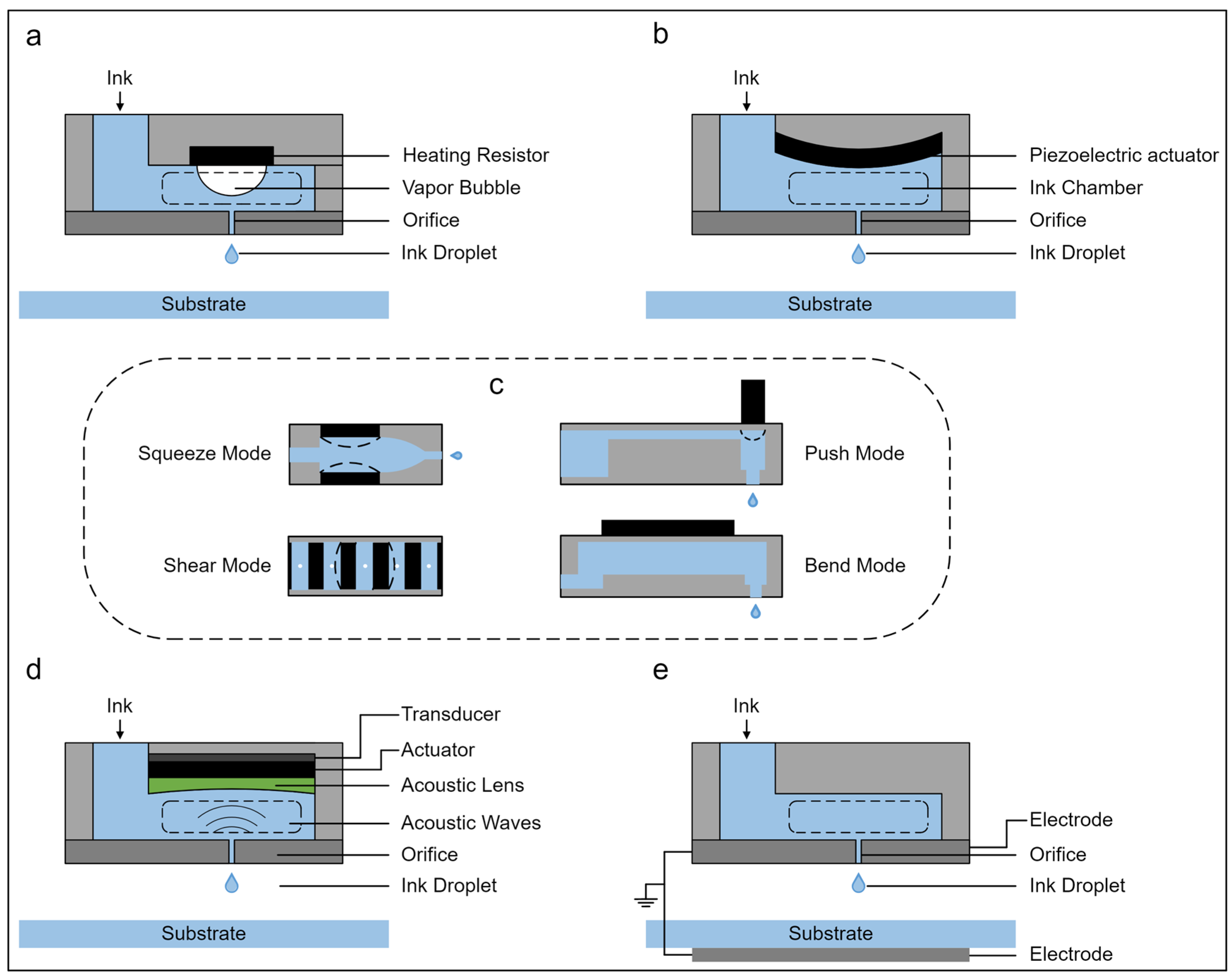
2.1.1. Inkjet Printing (IJP)
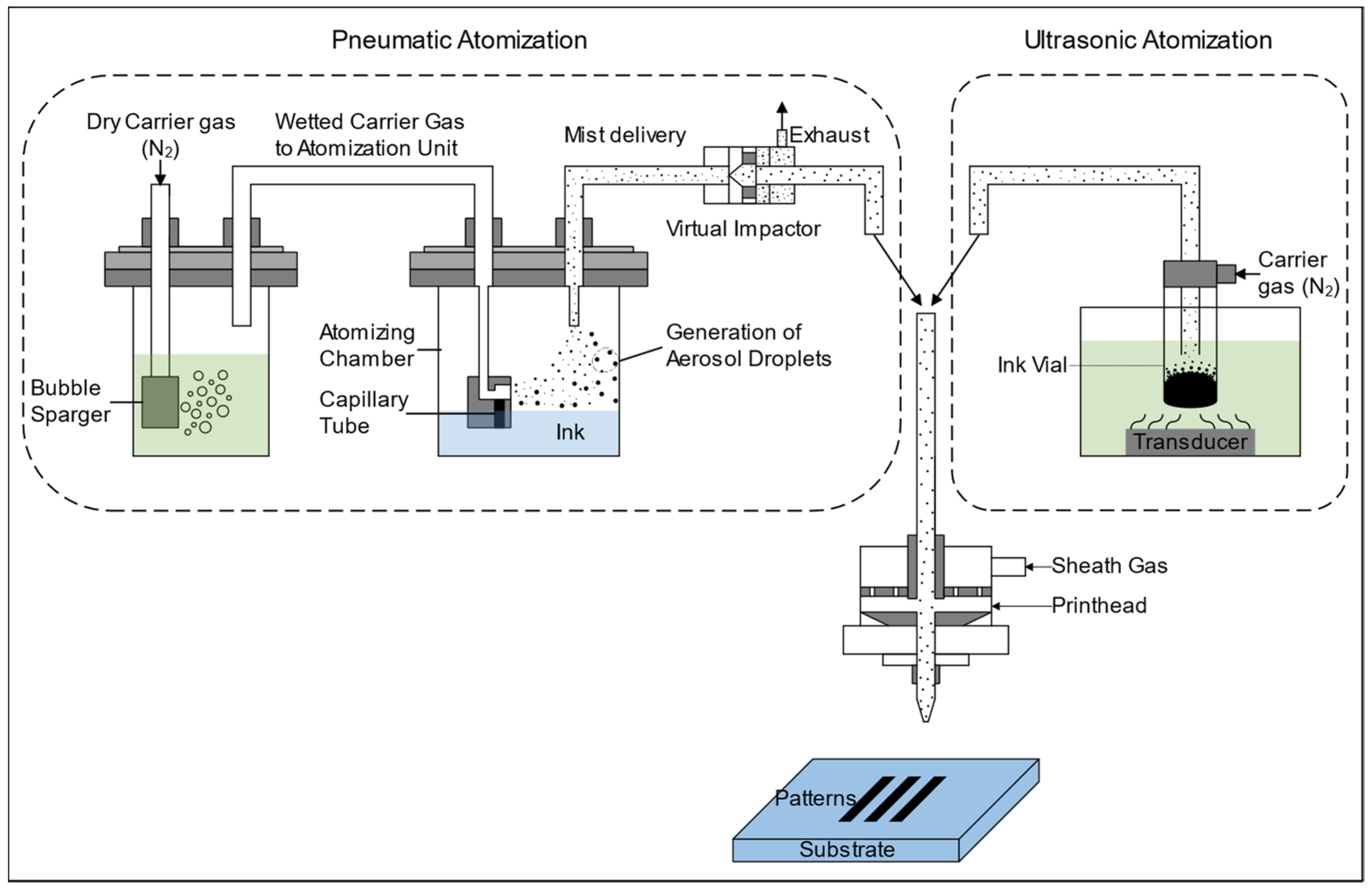
2.1.2. Aerosol Jet Printing (AJP)
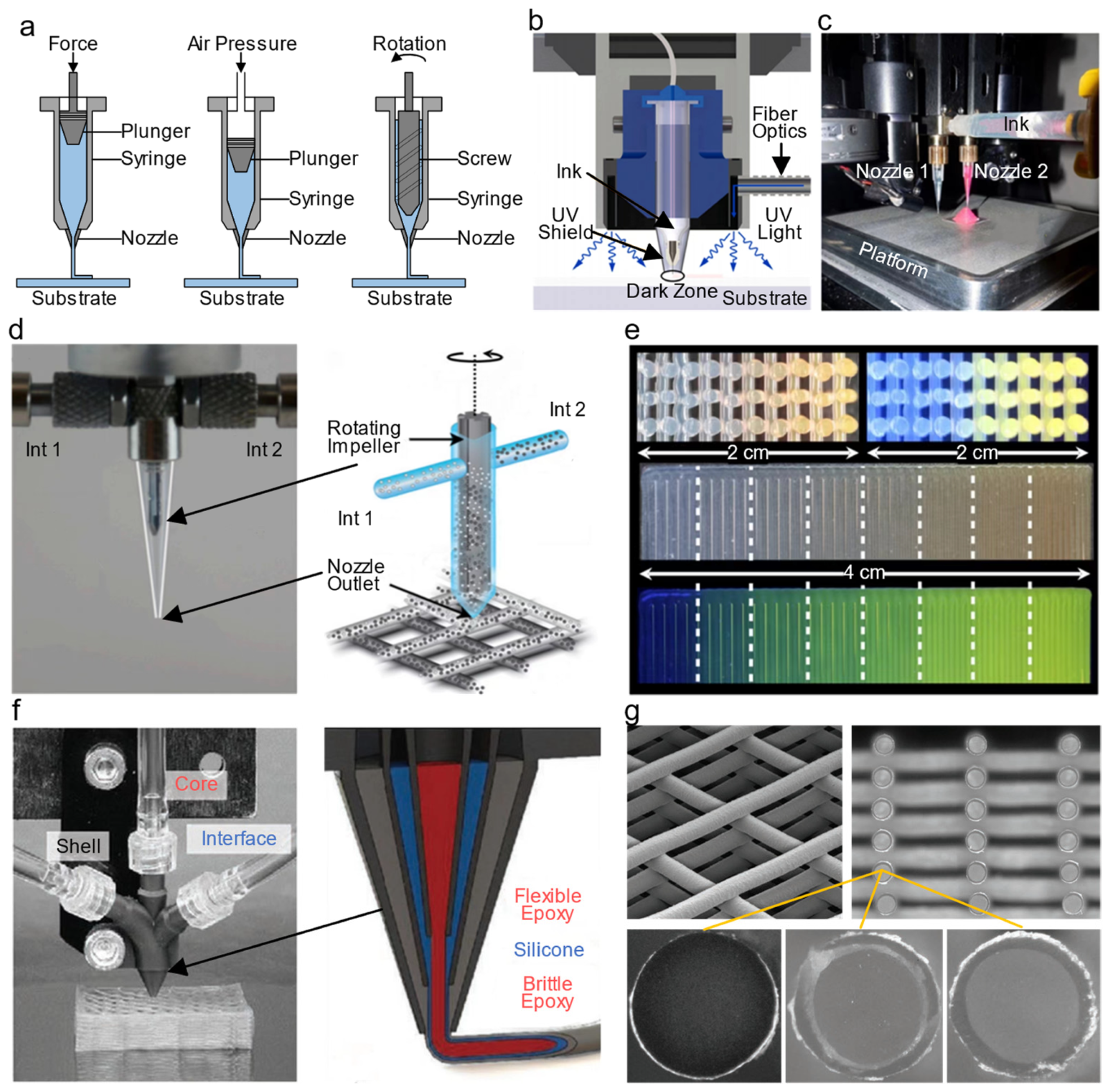
2.2. Direct Ink Writing (DIW)
2.3. Fused Deposition Modeling (FDM)
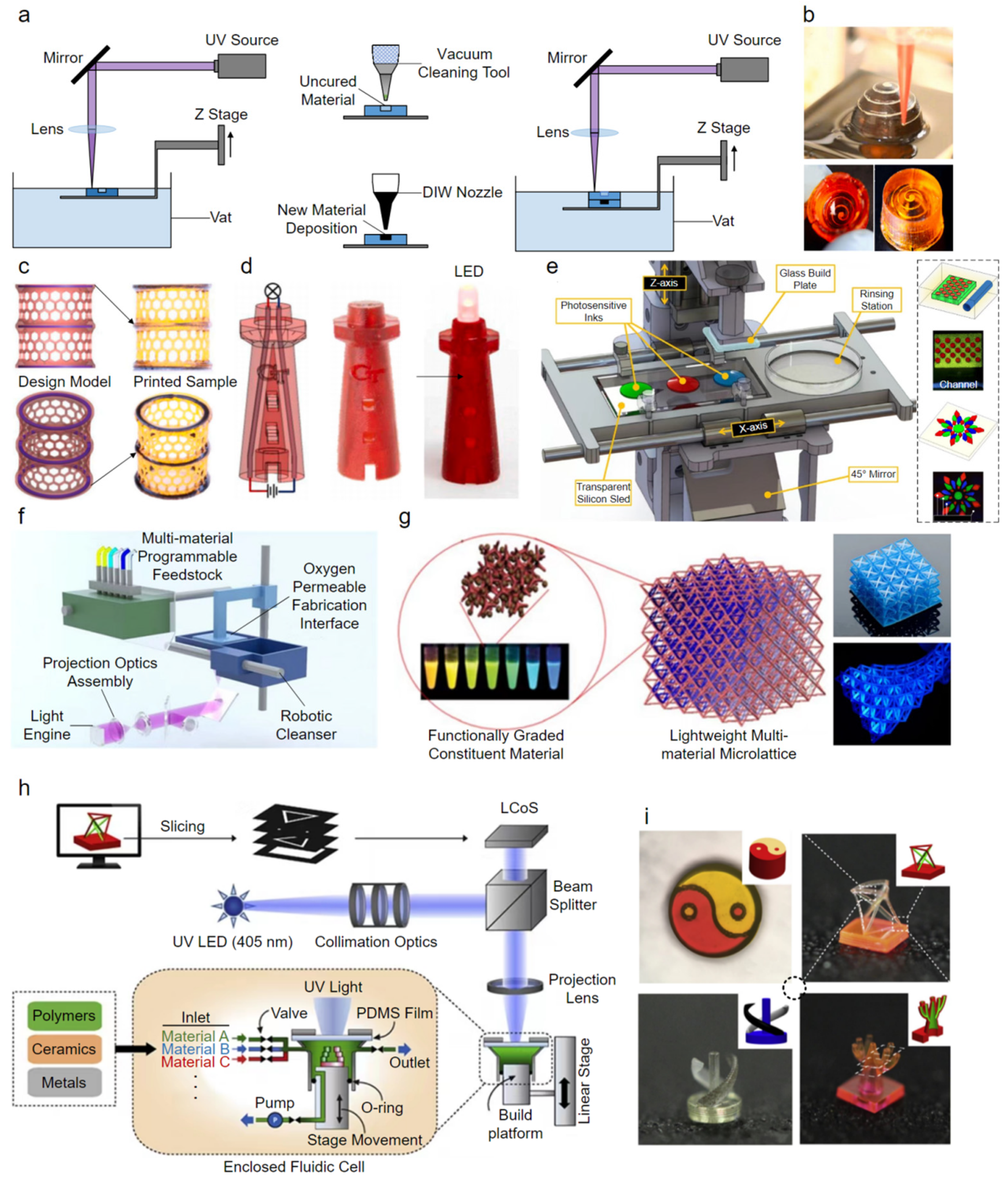
2.4. Vat Photopolymerization (VP)
3. Applications of Multi-Material 3D Printing in Functional Ceramic Devices
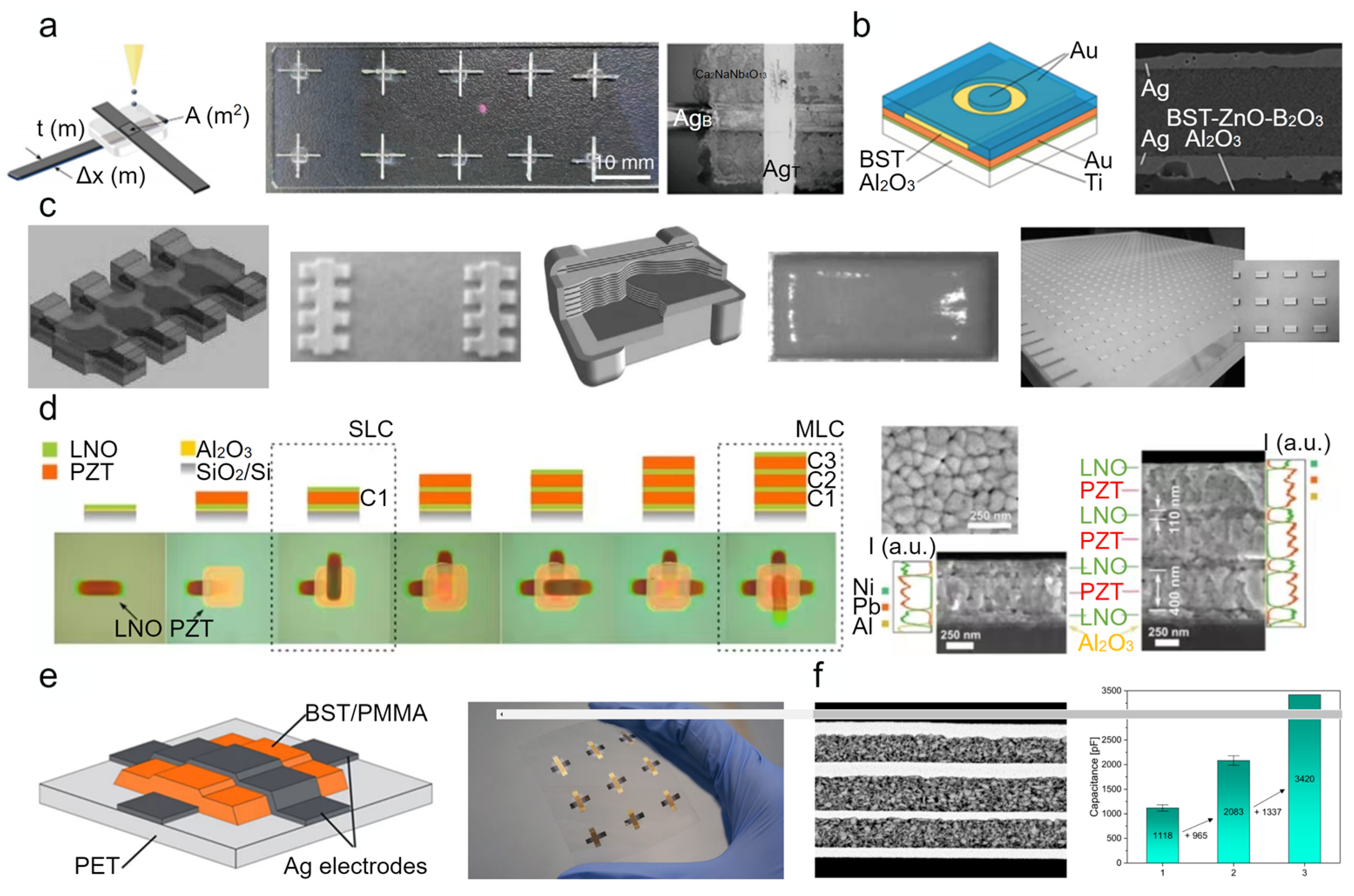
3.1. Capacitors
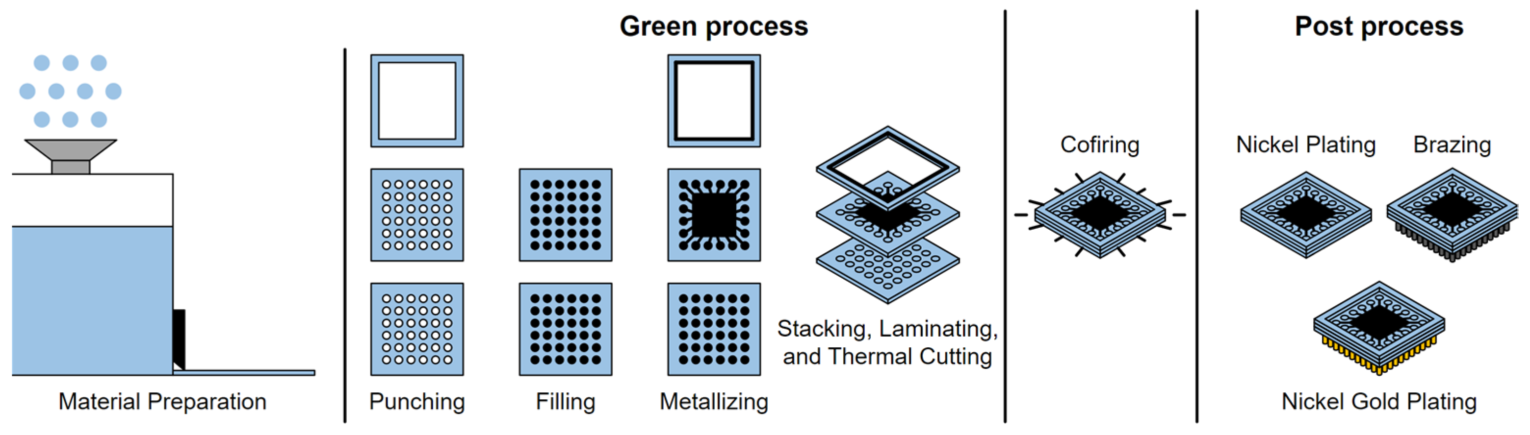
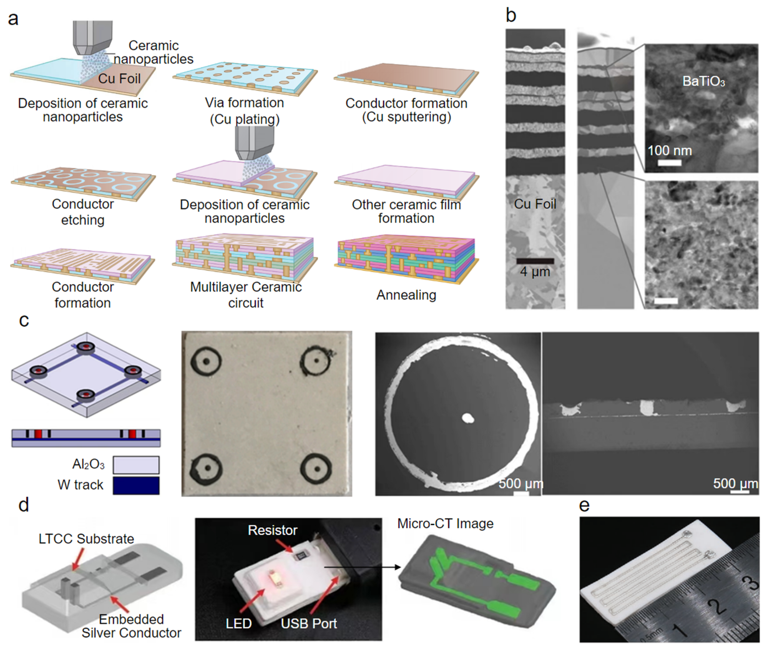
3.2. Multilayer Substrates
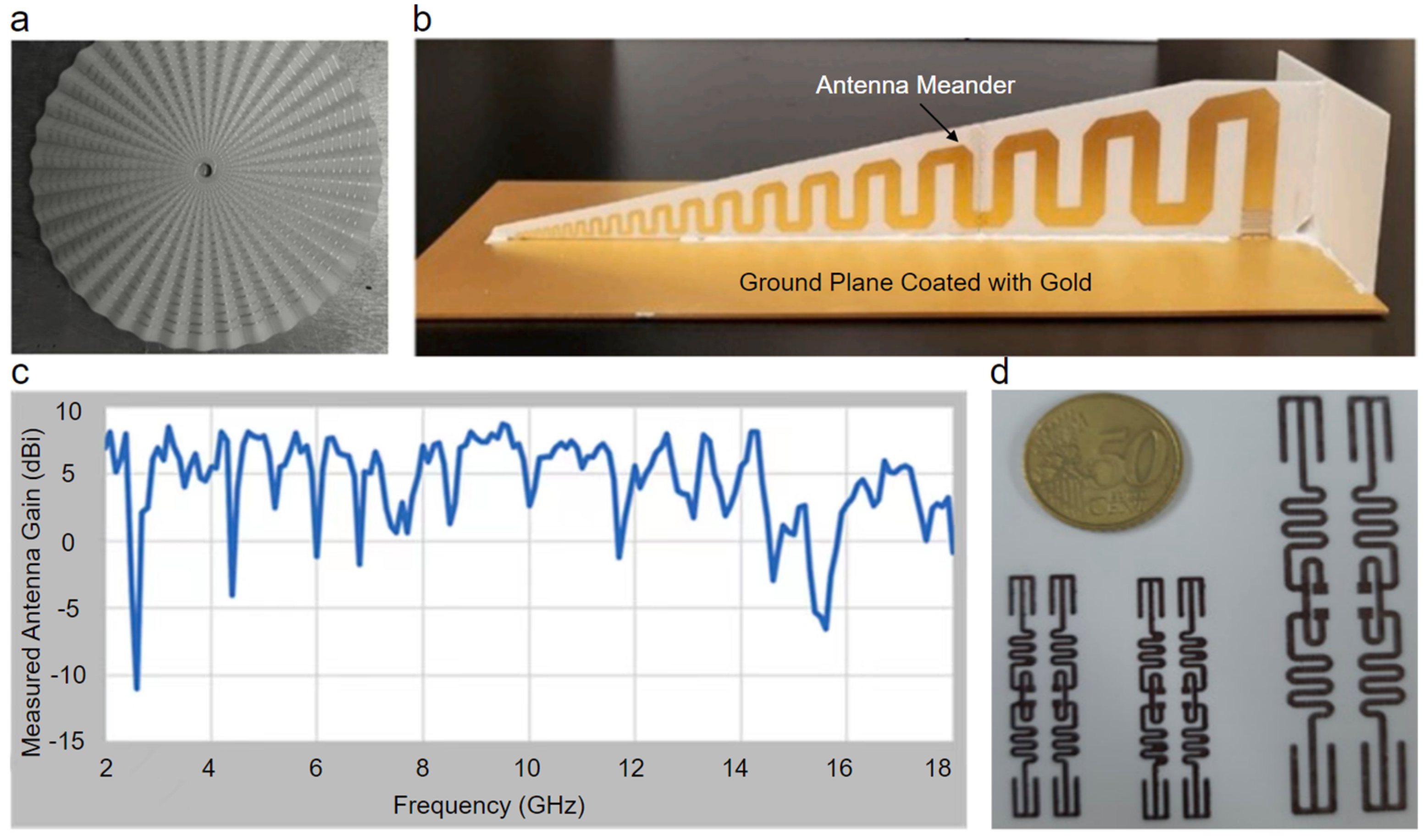
3.3. Microstrip Antennas
4. Conclusions and Outlook
Author Contributions
Funding
Institutional Review Board Statement
Data Availability Statement
Acknowledgments
Conflicts of Interest
References
- Yin, Q.; Zhu, B.; Zeng, H. Microstructure, Property and Processing of Functional Ceramics; Springer Science & Business Media: Berlin, Germany, 2010; pp. 1–6. [Google Scholar]
- Ruiz-Morales, J.; Tarancón, A.; Canales-Vázquez, J.; Méndez-Ramos, J.; Hernández-Afonso, L.; Acosta-Mora, P.; Rueda, J.R.M.; Fernández-González, R. Three dimensional printing of components and functional devices for energy and environmental applications. Energy Environ. Sci. 2017, 10, 846–859. [Google Scholar] [CrossRef] [Green Version]
- Pan, M.-J.; Randall, C.A. A brief introduction to ceramic capacitors. IEEE Electr. Insul. Mag. 2010, 26, 44–50. [Google Scholar] [CrossRef]
- Thelemann, T.; Bartnitzek, T.; Suphan, K.-H.; Apel, S. Advancing packaging solutions using 3D capabilities of ceramic multilayers. In Proceedings of the 2015 European Microelectronics Packaging Conference (EMPC), Friedrichshafen, Germany, 14–16 September 2015; pp. 1–6. [Google Scholar]
- Oshima, S.; Wada, K.; Murata, R.; Shimakata, Y. Multilayer Dual-Band Bandpass Filter in Low-Temperature Co-Fired Ceramic Substrate for Ultra-Wideband Applications. IEEE Trans. Microw. Theory Tech. 2010, 58, 614–623. [Google Scholar] [CrossRef]
- Liu, Z.; Wang, P.; Zeng, Z. Enhancement of the Gain for Microstrip Antennas Using Negative Permeability Metamaterial on Low Temperature Co-Fired Ceramic (LTCC) Substrate. IEEE Antennas Wirel. Propag. Lett. 2013, 12, 429–432. [Google Scholar] [CrossRef]
- Chen, H.; Che, W.; Wang, X.; Feng, W. Size-Reduced Planar and Nonplanar SIW Gysel Power Divider Based on Low Temperature Co-fired Ceramic Technology. IEEE Microw. Wirel. Compon. Lett. 2017, 27, 1065–1067. [Google Scholar] [CrossRef]
- Bhutani, A.; Gottel, B.; Lipp, A.; Zwick, T. Packaging Solution Based on Low-Temperature Cofired Ceramic Technology for Frequencies Beyond 100 GHz. IEEE Trans. Compon. Packag. Manuf. Technol. 2018, 9, 945–954. [Google Scholar] [CrossRef]
- Ren, L.; Luo, X.; Zhou, H. The tape casting process for manufacturing low-temperature co-fired ceramic green sheets: A review. J. Am. Ceram. Soc. 2018, 101, 3874–3889. [Google Scholar] [CrossRef]
- ISO/ASTM 52900:2015; Additive Manufacturing: General: Principles: Terminology. ISO: Geneva, Switzerland, 2015; pp. 1–19.
- Wolf, A.; Rosendahl, P.L.; Knaack, U. Additive manufacturing of clay and ceramic building components. Autom. Constr. 2021, 133, 103956. [Google Scholar] [CrossRef]
- He, Q.; Jiang, J.; Yang, X.; Zhang, L.; Zhou, Z.; Zhong, Y.; Shen, Z. Additive manufacturing of dense zirconia ceramics by fused deposition modeling via screw extrusion. J. Eur. Ceram. Soc. 2020, 41, 1033–1040. [Google Scholar] [CrossRef]
- Wang, F.; Li, Z.; Lou, Y.; Zeng, F.; Hao, M.; Lei, W.; Wang, X.; Wang, X.; Fan, G.; Lu, W. Stereolithographic additive manufacturing of Luneburg lens using Al2O3-based low sintering temperature ceramics for 5G MIMO antenna. Addit. Manuf. 2021, 47, 102244. [Google Scholar] [CrossRef]
- Liu, K.; Zhou, C.; Hu, J.; Zhang, S.; Zhang, Q.; Sun, C.; Shi, Y.; Sun, H.; Yin, C.; Zhang, Y.; et al. Fabrication of barium titanate ceramics via digital light processing 3D printing by using high refractive index monomer. J. Eur. Ceram. Soc. 2021, 41, 5909–5917. [Google Scholar] [CrossRef]
- Xing, H.; Zou, B.; Liu, X.; Wang, X.; Huang, C.; Hu, Y. Fabrication strategy of complicated Al2O3-Si3N4 functionally graded materials by stereolithography 3D printing. J. Eur. Ceram. Soc. 2020, 40, 5797–5809. [Google Scholar] [CrossRef]
- Khatri, B.; Lappe, K.; Habedank, M.; Mueller, T.; Megnin, C.; Hanemann, T. Fused Deposition Modeling of ABS-Barium Titanate Composites: A Simple Route towards Tailored Dielectric Devices. Polymers 2018, 10, 666. [Google Scholar] [CrossRef] [PubMed] [Green Version]
- Lee, J.-H.; Kim, J.-H.; Hwang, K.-T.; Hwang, H.-J.; Han, K.-S. Digital inkjet printing in three dimensions with multiple ceramic compositions. J. Eur. Ceram. Soc. 2020, 41, 1490–1497. [Google Scholar] [CrossRef]
- Gong, P.; Li, Y.; Xin, C.; Chen, Q.; Hao, L.; Sun, Q.; Li, Z. Multimaterial 3D-printing barium titanate/carbonyl iron composites with bilayer-gradient honeycomb structure for adjustable broadband microwave absorption. Ceram. Int. 2021, 48, 9873–9881. [Google Scholar] [CrossRef]
- Smay, J.E.; Nadkarni, S.S.; Xu, J. Direct Writing of Dielectric Ceramics and Base Metal Electrodes. Int. J. Appl. Ceram. Technol. 2007, 4, 47–52. [Google Scholar] [CrossRef]
- Truby, R.; Lewis, J.A. Printing soft matter in three dimensions. Nature 2016, 540, 371–378. [Google Scholar] [CrossRef]
- Han, D.; Lee, H. Recent advances in multi-material additive manufacturing: Methods and applications. Curr. Opin. Chem. Eng. 2020, 28, 158–166. [Google Scholar] [CrossRef]
- Wang, P.; Li, J.; Wang, G.; He, L.; Yu, Y.; Xu, B. Multimaterial Additive Manufacturing of LTCC Matrix and Silver Conductors for 3D Ceramic Electronics. Adv. Mater. Technol. 2022, 7, 2101462. [Google Scholar] [CrossRef]
- Oh, Y.; Bharambe, V.; Mummareddy, B.; Martin, J.; McKnight, J.; Abraham, M.A.; Walker, J.M.; Rogers, K.; Conner, B.; Cortes, P.; et al. Microwave dielectric properties of zirconia fabricated using NanoParticle Jetting™. Addit. Manuf. 2019, 27, 586–594. [Google Scholar] [CrossRef]
- Castrejon-Pita, J.R.; Baxter, W.; Morgan, J.; Temple, S.; Martin, G.; Hutchings, I.M. Future, opportunities and challenges of inkjet technologies. At. Sprays 2013, 23, 541–565. [Google Scholar] [CrossRef] [Green Version]
- Dilag, J.; Chen, T.; Li, S.; Bateman, S.A. Design and direct additive manufacturing of three-dimensional surface micro-structures using material jetting technologies. Addit. Manuf. 2019, 27, 167–174. [Google Scholar] [CrossRef]
- Choi, K.-H.; Yoo, J.; Lee, C.K.; Lee, S.-Y. All-inkjet-printed, solid-state flexible supercapacitors on paper. Energy Environ. Sci. 2016, 9, 2812–2821. [Google Scholar] [CrossRef]
- Craton, M.T.; Sorocki, J.; Piekarz, I.; Gruszczynski, S.; Wincza, K.; Papapolymerou, J. Realization of fully 3D printed W-band bandpass filters using aerosol jet printing technology. In Proceedings of the 2018 48th European Microwave Conference (EuMC), Madrid, Spain, 25–27 September 2018; pp. 1013–1016. [Google Scholar]
- Theiler, P.M.; Lütolf, F.; Ferrini, R. Non-contact printing of optical waveguides using capillary bridges. Opt. Express 2018, 26, 11934–11939. [Google Scholar] [CrossRef] [PubMed]
- Eggenhuisen, T.M.; Galagan, Y.; Biezemans, A.F.K.V.; Slaats, T.M.W.L.; Voorthuijzen, W.P.; Kommeren, S.; Shanmugam, S.; Teunissen, J.P.; Hadipour, A.; Verhees, W.J.H.; et al. High efficiency, fully inkjet printed organic solar cells with freedom of design. J. Mater. Chem. A 2015, 3, 7255–7262. [Google Scholar] [CrossRef] [Green Version]
- Qin, H.; Dong, J.; Lee, Y.-S. Fabrication and electrical characterization of multi-layer capacitive touch sensors on flexible substrates by additive e-jet printing. J. Manuf. Process. 2017, 28, 479–485. [Google Scholar] [CrossRef]
- Khan, A.; Rahman, K.; Ali, S.; Khan, S.; Wang, B.; Bermak, A. Fabrication of circuits by multi-nozzle electrohydrodynamic inkjet printing for soft wearable electronics. J. Mater. Res. 2021, 36, 3568–3578. [Google Scholar] [CrossRef]
- Laurila, M.-M.; Khorramdel, B.; Mantysalo, M. Combination of E-Jet and Inkjet Printing for Additive Fabrication of Multilayer High-Density RDL of Silicon Interposer. IEEE Trans. Electron Devices 2017, 64, 1217–1224. [Google Scholar] [CrossRef]
- Karim, N.; Afroj, S.; Tan, S.; Novoselov, K.S.; Yeates, S.G. All Inkjet-Printed Graphene-Silver Composite Ink on Textiles for Highly Conductive Wearable Electronics Applications. Sci. Rep. 2019, 9, 8035. [Google Scholar] [CrossRef] [Green Version]
- Kant, T.; Shrivas, K.; Tapadia, K.; Devi, R.; Ganesan, V.; Deb, M.K. Inkjet-printed paper-based electrochemical sensor with gold nano-ink for detection of glucose in blood serum. New J. Chem. 2021, 45, 8297–8305. [Google Scholar] [CrossRef]
- Khan, S.; Nguyen, T.; Lubej, M.; Thiery, L.; Vairac, P.; Briand, D. Low-power printed micro-hotplates through aerosol jetting of gold on thin polyimide membranes. Microelectron. Eng. 2018, 194, 71–78. [Google Scholar] [CrossRef]
- Lim, S.; Joyce, M.; Fleming, P.D.; Aijazi, A.T.; Atashbar, M. Inkjet Printing and Sintering of Nano-Copper Ink. J. Imaging Sci. Technol. 2013, 57, 50506-1–50506-7. [Google Scholar] [CrossRef]
- Khan, A.; Rahman, K.; Kim, D.S.; Choi, K.H. Direct printing of copper conductive micro-tracks by multi-nozzle electrohydrodynamic inkjet printing process. J. Mater. Process. Technol. 2011, 212, 700–706. [Google Scholar] [CrossRef]
- Majee, S.; Karlsson, M.C.F.; Wojcik, P.J.; Sawatdee, A.; Mulla, M.Y.; Alvi, N.U.H.; Dyreklev, P.; Beni, V.; Nilsson, D. Low temperature chemical sintering of inkjet-printed Zn nanoparticles for highly conductive flexible electronic components. npj Flex. Electron. 2021, 5, 32. [Google Scholar] [CrossRef]
- Mahajan, B.K.; Ludwig, B.; Shou, W.; Yu, X.; Fregene, E.; Xu, H.; Pan, H.; Huang, X. Aerosol printing and photonic sintering of bioresorbable zinc nanoparticle ink for transient electronics manufacturing. Sci. China Inf. Sci. 2018, 61, 060412. [Google Scholar] [CrossRef]
- Singh, A.; Katiyar, M.; Garg, A. Understanding the formation of PEDOT:PSS films by ink-jet printing for organic solar cell applications. RSC Adv. 2015, 5, 78677–78685. [Google Scholar] [CrossRef] [Green Version]
- Zips, S.; Grob, L.; Rinklin, P.; Terkan, K.; Adly, N.Y.; Weiß, L.J.K.; Mayer, D.; Wolfrum, B. Fully Printed μ-Needle Electrode Array from Conductive Polymer Ink for Bioelectronic Applications. ACS Appl. Mater. Interfaces 2019, 11, 32778–32786. [Google Scholar] [CrossRef]
- Yang, C.-Y.; Stoeckel, M.-A.; Ruoko, T.-P.; Wu, H.-Y.; Liu, X.; Kolhe, N.B.; Wu, Z.; Puttisong, Y.; Musumeci, C.; Massetti, M.; et al. A high-conductivity n-type polymeric ink for printed electronics. Nat. Commun. 2021, 12, 2354. [Google Scholar] [CrossRef]
- McKerricher, G.; Maller, R.; Mohammad, V.; McLachlan, M.A.; Shamim, A. Inkjet-printed thin film radio-frequency capacitors based on sol-gel derived alumina dielectric ink. Ceram. Int. 2017, 43, 9846–9853. [Google Scholar] [CrossRef] [Green Version]
- Lim, J.; Jung, H.; Baek, C.; Hwang, G.-T.; Ryu, J.; Yoon, D.; Yoo, J.; Park, K.-I.; Kim, J.H. All-inkjet-printed flexible piezoelectric generator made of solvent evaporation assisted BaTiO3 hybrid material. Nano Energy 2017, 41, 337–343. [Google Scholar] [CrossRef]
- Craton, M.T.; He, Y.; Roch, A.; Chahal, P.; Papapolymerou, J. Additively manufactured interdigitated capacitors using barium titanate nanocomposite inks. In Proceedings of the 2019 49th European Microwave Conference (EuMC), Paris, France, 1–3 October 2019; pp. 488–491. [Google Scholar]
- Rahul, S.; Balasubramanian, K.; Venkatesh, S. Optimizing inkjet printing process to fabricate thick ceramic coatings. Ceram. Int. 2017, 43, 4513–4519. [Google Scholar] [CrossRef]
- Özkol, E.; Wätjen, A.M.; Bermejo, R.; Deluca, M.; Ebert, J.; Danzer, R.; Telle, R. Mechanical characterisation of miniaturised direct inkjet printed 3Y-TZP specimens for microelectronic applications. J. Eur. Ceram. Soc. 2010, 30, 3145–3152. [Google Scholar] [CrossRef]
- Zhu, Z.; Zhang, J.; Zhou, Z.; Ning, H.; Cai, W.; Wei, J.; Zhou, S.; Yao, R.; Lu, X.; Peng, J. A Simple, Low Cost Ink System for Drop-on-Demand Printing High Performance Metal Oxide Dielectric Film at Low Temperature. ACS Appl. Mater. Interfaces 2019, 11, 5193–5199. [Google Scholar] [CrossRef] [PubMed]
- Awais, M.N.; Kim, H.C.; Doh, Y.H.; Choi, K.H. ZrO2 flexible printed resistive (memristive) switch through electrohydrodynamic printing process. Thin Solid Films 2013, 536, 308–312. [Google Scholar] [CrossRef]
- Huckaba, A.J.; Lee, Y.; Xia, R.; Paek, S.; Bassetto, V.C.; Oveisi, E.; Lesch, A.; Kinge, S.; Dyson, P.J.; Girault, H.; et al. Inkjet-Printed Mesoporous TiO2 and Perovskite Layers for High Efficiency Perovskite Solar Cells. Energy Technol. 2018, 7, 317–324. [Google Scholar] [CrossRef] [Green Version]
- Padrón-Hernández, W.; Ceballos-Chuc, M.C.; Pourjafari, D.; Oskam, G.; Tinoco, J.C.; Martínez-López, A.; Rodríguez-Gattorno, G. Stable inks for inkjet printing of TiO2 thin films. Mater. Sci. Semicond. Process. 2018, 81, 75–81. [Google Scholar] [CrossRef]
- Mikolajek, M.; Friederich, A.; Kohler, C.; Rosen, M.; Rathjen, A.; Krüger, K.; Binder, J.R. Direct Inkjet Printing of Dielectric Ceramic/Polymer Composite Thick Films. Adv. Eng. Mater. 2015, 17, 1294–1301. [Google Scholar] [CrossRef]
- Wu, X.; Fei, F.; Chen, Z.; Su, W.; Cui, Z. A new nanocomposite dielectric ink and its application in printed thin-film transistors. Compos. Sci. Technol. 2014, 94, 117–122. [Google Scholar] [CrossRef]
- Singlard, M.; Aimable, A.; Lejeune, M.; Dossou-Yovo, C.; Poncelet, M.; Noguera, R.; Modes, C. Aqueous suspensions of glass silicate dielectric powders for ink-jet printing applications. Powder Technol. 2014, 266, 303–311. [Google Scholar] [CrossRef]
- Zhang, F.; Tuck, C.; Hague, R.; He, Y.; Saleh, E.; Li, Y.; Sturgess, C.; Wildman, R. Inkjet printing of polyimide insulators for the 3D printing of dielectric materials for microelectronic applications. J. Appl. Polym. Sci. 2016, 133, 43361–43371. [Google Scholar] [CrossRef]
- Yi, L.; Torah, R.; Beeby, S.; Tudor, J. An all-inkjet printed flexible capacitor on a textile using a new poly(4-vinylphenol) dielectric ink for wearable applications. In Proceedings of the Sensors, Taipei, Taiwan, 28–31 October 2012. [Google Scholar]
- Jung, C.; Tang, X.; Kwon, H.-J.; Wang, R.; Oh, S.M.; Ye, H.; Jeong, Y.R.; Jeong, Y.J.; Kim, S.H. Electrohydrodynamic-Printed Polyvinyl Alcohol-Based Gate Insulators for Organic Integrated Devices. Adv. Eng. Mater. 2022, 24, 2100900. [Google Scholar] [CrossRef]
- Hoath, S.D. Fundamentals of Inkjet Printing: The Science of Inkjet and Droplets; John Wiley & Sons: Weinheim, Germany, 2016; pp. 1–11. [Google Scholar]
- Rosa, M.; Barou, C.; Esposito, V. Zirconia UV-curable colloids for additive manufacturing via hybrid inkjet printing-stereolithography. Mater. Lett. 2018, 215, 214–217. [Google Scholar] [CrossRef]
- Hon, K.K.B.; Li, L.; Hutchings, I.M. Direct writing technology—Advances and developments. CIRP Ann. 2008, 57, 601–620. [Google Scholar] [CrossRef]
- Tan, H.W.; Choong, Y.Y.C.; Kuo, C.N.; Low, H.Y.; Chua, C.K. 3D printed electronics: Processes, materials and future trends. Prog. Mater. Sci. 2022, 127, 100945. [Google Scholar] [CrossRef]
- Wijshoff, H. The dynamics of the piezo inkjet printhead operation. Phys. Rep. 2010, 491, 77–177. [Google Scholar] [CrossRef]
- Gibson, I.; Rosen, D.W.; Stucker, B.; Khorasani, M.; Rosen, D.; Stucker, B.; Khorasani, M. Additive Manufacturing Technologies; Springer: Berlin/Heidelberg, Germany, 2021; Volume 17. [Google Scholar]
- Shah, M.A.; Lee, D.-G.; Lee, B.-Y.; Hur, S. Classifications and Applications of Inkjet Printing Technology: A Review. IEEE Access 2021, 9, 140079–140102. [Google Scholar] [CrossRef]
- Mogalicherla, A.K.; Lee, S.; Pfeifer, P.; Dittmeyer, R. Drop-on-demand inkjet printing of alumina nanoparticles in rectangular microchannels. Microfluid. Nanofluid. 2013, 16, 655–666. [Google Scholar] [CrossRef]
- Lang, V.; Weingarten, S.; Wiemer, H.; Scheithauer, U.; Glausch, F.; Johne, R.; Michaelis, A.; Ihlenfeldt, S. Process Data-Based Knowledge Discovery in Additive Manufacturing of Ceramic Materials by Multi-Material Jetting (CerAM MMJ). J. Manuf. Mater. Process. 2020, 4, 74. [Google Scholar] [CrossRef]
- Lall, P.; Abrol, A.; Kothari, N.; Leever, B.; Miller, S. Process Capability of Aerosol-Jet Additive Processes for Long-Runs Up to 10-Hours. J. Electron. Packag. 2020, 142, 041003. [Google Scholar] [CrossRef]
- Gardini, D.; Blosi, M.; Zanelli, C.; Dondi, M. Ceramic Ink-Jet Printing for Digital Decoration: Physical Constraints for Ink Design. J. Nanosci. Nanotechnol. 2015, 15, 3552–3561. [Google Scholar] [CrossRef]
- Polsakiewicz, D.A.; Kollenberg, W. Highly loaded alumina inks for use in a piezoelectric print head. Mater. Werkst. 2011, 42, 812–819. [Google Scholar] [CrossRef]
- Fromm, J.E. Numerical Calculation of the Fluid Dynamics of Drop-on-Demand Jets. IBM J. Res. Dev. 1984, 28, 322–333. [Google Scholar] [CrossRef]
- Reis, N.; Derby, B. Ink jet deposition of ceramic suspensions: Modeling and experiments of droplet formation. MRS Online Proc. Libr. 2000, 625, 117. [Google Scholar] [CrossRef]
- Bonaccorso, F.; Bartolotta, A.; Coleman, J.N.; Backes, C. 2D-Crystal-Based Functional Inks. Adv. Mater. 2016, 28, 6136–6166. [Google Scholar] [CrossRef]
- Derby, B. Inkjet printing ceramics: From drops to solid. J. Eur. Ceram. Soc. 2011, 31, 2543–2550. [Google Scholar] [CrossRef]
- Jang, D.; Kim, D.; Moon, J. Influence of Fluid Physical Properties on Ink-Jet Printability. Langmuir 2009, 25, 2629–2635. [Google Scholar] [CrossRef]
- Mikolajek, M.; Friedrich, A.; Bauer, W.; Binder, J. Requirements to ceramic suspensions for inkjet printing. Ceram. Forum Int. 2015, 92, E25–E29. [Google Scholar]
- Lejeune, M.; Chartier, T.; Dossou-Yovo, C.; Noguera, R. Ink-jet printing of ceramic micro-pillar arrays. J. Eur. Ceram. Soc. 2009, 29, 905–911. [Google Scholar] [CrossRef]
- Arango, I.; Cañas, M. Dynamic analysis of a recirculation system of micro functional fluids for ink-jet applications. Microsyst. Technol. 2017, 23, 1485–1494. [Google Scholar] [CrossRef]
- Goswami, A.; Ankit, K.; Balashanmugam, N.; Umarji, A.M.; Madras, G. Optimization of rheological properties of photopolymerizable alumina suspensions for ceramic microstereolithography. Ceram. Int. 2014, 40, 3655–3665. [Google Scholar] [CrossRef]
- Seidel, J.; Claussen, N.; Rödel, J. Reliability of alumina ceramics: Effect of grain size. J. Eur. Ceram. Soc. 1995, 15, 395–404. [Google Scholar] [CrossRef]
- Eichler, J.; Rödel, J.; Eisele, U.; Hoffman, M. Effect of Grain Size on Mechanical Properties of Submicrometer 3Y-TZP: Fracture Strength and Hydrothermal Degradation. J. Am. Ceram. Soc. 2007, 90, 2830–2836. [Google Scholar] [CrossRef]
- Yang, Z.; Gao, F.; Du, H.; Jin, L.; Yan, L.; Hu, Q.; Yu, Y.; Qu, S.; Wei, X.; Xu, Z.; et al. Grain size engineered lead-free ceramics with both large energy storage density and ultrahigh mechanical properties. Nano Energy 2019, 58, 768–777. [Google Scholar] [CrossRef]
- Mudinepalli, V.R.; Feng, L.; Lin, W.-C.; Murty, B.S. Effect of grain size on dielectric and ferroelectric properties of nanostructured Ba0.8Sr0.2TiO3 ceramics. J. Adv. Ceram. 2015, 4, 46–53. [Google Scholar] [CrossRef] [Green Version]
- Hanani, Z.; Mezzane, D.; Amjoud, M.; Fourcade, S.; Razumnaya, A.; Luk’Yanchuk, I.; Gouné, M. Enhancement of dielectric properties of lead-free BCZT ferroelectric ceramics by grain size engineering. Superlattices Microstruct. 2019, 127, 109–117. [Google Scholar] [CrossRef] [Green Version]
- Lim, J.; Kim, J.; Yoon, Y.J.; Kim, H.; Yoon, H.G.; Lee, S.-N.; Kim, J.-H. Improvement on Relative Permittivity of Inkjet-Printed BaTiO3-Resin Hybrid Film by Manipulating Ceramic Powder Size-Distribution. Int. J. Appl. Ceram. Technol. 2012, 9, 199–205. [Google Scholar] [CrossRef]
- Zhu, Z.; Gong, Z.; Qu, P.; Li, Z.; Rasaki, S.A.; Liu, Z.; Wang, P.; Liu, C.; Lao, C.; Chen, Z. Additive manufacturing of thin electrolyte layers via inkjet printing of highly-stable ceramic inks. J. Adv. Ceram. 2021, 10, 279–290. [Google Scholar] [CrossRef]
- Wätjen, A.M.; Gingter, P.; Kramer, M.; Telle, R. Novel Prospects and Possibilities in Additive Manufacturing of Ceramics by means of Direct Inkjet Printing. Adv. Mech. Eng. 2014, 6, 141346. [Google Scholar] [CrossRef] [Green Version]
- Oliver, D.R.; Ward, S.G. Relationship between Relative Viscosity and Volume Concentration of Stable Suspensions of Spherical Particles. Nature 1953, 171, 396–397. [Google Scholar] [CrossRef]
- Roscoe, R. The viscosity of suspensions of rigid spheres. Br. J. Appl. Phys. 1952, 3, 267–269. [Google Scholar] [CrossRef]
- Mooney, M. The viscosity of a concentrated suspensions of spherical particles. J. Colloid Sci. 1951, 6, 162–170. [Google Scholar] [CrossRef]
- Krieger, I.M.; Dougherty, T.J. A Mechanism for Non-Newtonian Flow in Suspensions of Rigid Spheres. Trans. Soc. Rheol. 1959, 3, 137–152. [Google Scholar] [CrossRef]
- Chong, J.; Christiansen, E.; Baer, A. Rheology of concentrated suspensions. J. Appl. Polym. Sci. 1971, 15, 2007–2021. [Google Scholar] [CrossRef]
- Dabak, T.; Yucel, O. Shear viscosity behavior of highly concentrated suspensions at low and high shear-rates. Rheol. Acta 1986, 25, 527–533. [Google Scholar] [CrossRef]
- Quemada, D. Rheology of concentrated disperse systems and minimum energy dissipation principle. Rheol. Acta 1977, 16, 82–94. [Google Scholar] [CrossRef]
- Brouwers, H.J.H. Viscosity of a concentrated suspension of rigid monosized particles. Phys. Rev. E 2010, 81, 051402. [Google Scholar] [CrossRef] [Green Version]
- Horri, B.A.; Ranganathan, P.; Selomulya, C.; Wang, H. A new empirical viscosity model for ceramic suspensions. Chem. Eng. Sci. 2011, 66, 2798–2806. [Google Scholar] [CrossRef]
- Hoey, J.M.; Lutfurakhmanov, A.; Schulz, D.L.; Akhatov, I.S. A Review on Aerosol-Based Direct-Write and Its Applications for Microelectronics. J. Nanotechnol. 2012, 2012, 324380. [Google Scholar] [CrossRef] [Green Version]
- Wilkinson, N.J.; Smith, M.A.A.; Kay, R.W.; Harris, R.A. A review of aerosol jet printing—A non-traditional hybrid process for micro-manufacturing. Int. J. Adv. Manuf. Technol. 2019, 105, 4599–4619. [Google Scholar] [CrossRef] [Green Version]
- Avvaru, B.; Patil, M.N.; Gogate, P.R.; Pandit, A.B. Ultrasonic atomization: Effect of liquid phase properties. Ultrasonics 2006, 44, 146–158. [Google Scholar] [CrossRef]
- Zhang, Y.; Yuan, S.; Wang, L. Investigation of capillary wave, cavitation and droplet diameter distribution during ultrasonic atomization. Exp. Therm. Fluid Sci. 2020, 120, 110219. [Google Scholar] [CrossRef]
- Kudo, T.; Sekiguchi, K.; Sankoda, K.; Namiki, N.; Nii, S. Effect of ultrasonic frequency on size distributions of nanosized mist generated by ultrasonic atomization. Ultrason. Sonochemistry 2017, 37, 16–22. [Google Scholar] [CrossRef] [PubMed]
- Lall, P.; Goyal, K.; Kothari, N.; Leever, B.; Miller, S. Additively Printed Multilayer Substrate Using Aerosol-Jet Technique. J. Electron. Packag. 2020, 142, 041110. [Google Scholar] [CrossRef]
- Sarobol, P.; Cook, A.; Clem, P.G.; Keicher, D.; Hirschfeld, D.; Hall, A.C.; Bell, N.S. Additive Manufacturing of Hybrid Circuits. Annu. Rev. Mater. Sci. 2016, 46, 41–62. [Google Scholar] [CrossRef]
- Deiner, L.J.; Reitz, T.L. Inkjet and Aerosol Jet Printing of Electrochemical Devices for Energy Conversion and Storage. Adv. Eng. Mater. 2017, 19, 1600878. [Google Scholar] [CrossRef]
- Secor, E.B. Guided ink and process design for aerosol jet printing based on annular drying effects. Flex. Print. Electron. 2018, 3, 035007. [Google Scholar] [CrossRef]
- Mahajan, A.; Frisbie, C.D.; Francis, L.F. Optimization of Aerosol Jet Printing for High-Resolution, High-Aspect Ratio Silver Lines. ACS Appl. Mater. Interfaces 2013, 5, 4856–4864. [Google Scholar] [CrossRef]
- Smith, M.; Choi, Y.S.; Boughey, C.; Kar-Narayan, S. Controlling and assessing the quality of aerosol jet printed features for large area and flexible electronics. Flex. Print. Electron. 2017, 2, 015004. [Google Scholar] [CrossRef]
- Arsenov, P.; Efimov, A.; Ivanov, V. Optimizing Aerosol Jet Printing Process of Platinum Ink for High-Resolution Conductive Microstructures on Ceramic and Polymer Substrates. Polymers 2021, 13, 918. [Google Scholar] [CrossRef]
- Mary Sukeshini, A.; Meisenkothen, F.; Gardner, P.; Reitz, T.L. Aerosol Jet® Printing of functionally graded SOFC anode interlayer and microstructural investigation by low voltage scanning electron microscopy. J. Power Sources 2013, 224, 295–303. [Google Scholar] [CrossRef]
- Tarabella, G.; Vurro, D.; Lai, S.; D’Angelo, P.; Ascari, L.; Iannotta, S. Aerosol jet printing of PEDOT:PSS for large area flexible electronics. Flex. Print. Electron. 2020, 5, 014005. [Google Scholar] [CrossRef]
- Akhatov, I.; Hoey, J.; Swenson, O.; Schulz, D. Aerosol focusing in micro-capillaries: Theory and experiment. J. Aerosol Sci. 2008, 39, 691–709. [Google Scholar] [CrossRef]
- Salary, R.R.; Lombardi, J.P.; Samie Tootooni, M.; Donovan, R.; Rao, P.K.; Borgesen, P.; Poliks, M.D. Computational Fluid Dynamics Modeling and Online Monitoring of Aerosol Jet Printing Process. J. Manuf. Sci. Eng. 2017, 139, 021015. [Google Scholar] [CrossRef]
- Binder, S.; Glatthaar, M.; Rädlein, E. Analytical Investigation of Aerosol Jet Printing. Aerosol Sci. Technol. 2014, 48, 924–929. [Google Scholar] [CrossRef] [Green Version]
- Tafoya, R.R.; Secor, E.B. Understanding effects of printhead geometry in aerosol jet printing. Flex. Print. Electron. 2020, 5, 035004. [Google Scholar] [CrossRef]
- Feng, J.Q.; Ramm, A.; Renn, M.J. A quantitative analysis of overspray in Aerosol Jet® printing. Flex. Print. Electron. 2021, 6, 045006. [Google Scholar] [CrossRef]
- Chen, G.; Gu, Y.; Tsang, H.; Hines, D.R.; Das, S. The Effect of Droplet Sizes on Overspray in Aerosol-Jet Printing. Adv. Eng. Mater. 2018, 20, 1701084. [Google Scholar] [CrossRef]
- Secor, E.B. Principles of aerosol jet printing. Flex. Print. Electron. 2018, 3, 035002. [Google Scholar] [CrossRef]
- Zhang, H.; Moon, S.K.; Ngo, T.H. Hybrid Machine Learning Method to Determine the Optimal Operating Process Window in Aerosol Jet 3D Printing. ACS Appl. Mater. Interfaces 2019, 11, 17994–18003. [Google Scholar] [CrossRef]
- Zhang, H.; Choi, J.P.; Moon, S.K.; Ngo, T.H. A multi-objective optimization framework for aerosol jet customized line width printing via small data set and prediction uncertainty. J. Mater. Process. Technol. 2020, 285, 116779. [Google Scholar] [CrossRef]
- Sun, H.; Wang, K.; Li, Y.; Zhang, C.; Jin, R. Quality Modeling of Printed Electronics in Aerosol Jet Printing Based on Microscopic Images. J. Manuf. Sci. Eng. 2017, 139, 071012. [Google Scholar] [CrossRef]
- Holness, F.B.; Price, A.D. Direct ink writing of 3D conductive polyaniline structures and rheological modelling. Smart Mater. Struct. 2017, 27, 015006. [Google Scholar] [CrossRef]
- Gu, S.; Tian, Y.; Liang, K.; Ji, Y. Chitin nanocrystals assisted 3D printing of polycitrate thermoset bioelastomers. Carbohydr. Polym. 2021, 256, 117549. [Google Scholar] [CrossRef] [PubMed]
- Jiang, Q.; Yang, D.; Yuan, H.; Wang, R.; Hao, M.; Ren, W.; Shao, G.; Wang, H.; Cui, J.; Hu, J. Fabrication and properties of Si2N2O-Si3N4 ceramics via direct ink writing and low-temperature sintering. Ceram. Int. 2021, 48, 32–41. [Google Scholar] [CrossRef]
- Xu, C.; Quinn, B.; Lebel, L.L.; Therriault, D.; L’Espérance, G. Multi-material direct ink writing (DIW) for complex 3D metallic structures with removable supports. ACS Appl. Mater. Interfaces 2019, 11, 8499–8506. [Google Scholar] [CrossRef]
- Li, Z.; Li, Y.; Shi, B.; Tang, D.; Wang, Y.; Hao, L. Dual gradient direct ink writing of functional geopolymer-based carbonyl-iron/graphene composites for adjustable broadband microwave absorption. Ceram. Int. 2022, 48, 9277–9285. [Google Scholar] [CrossRef]
- Luo, B.; Wei, Y.; Chen, H.; Zhu, Z.; Fan, P.; Xu, X.; Xie, B. Printing Carbon Nanotube-Embedded Silicone Elastomers via Direct Writing. ACS Appl. Mater. Interfaces 2018, 10, 44796–44802. [Google Scholar] [CrossRef]
- Cheng, M.; Ramasubramanian, A.; Rasul, G.; Jiang, Y.; Yuan, Y.; Foroozan, T.; Deivanayagam, R.; Saray, M.T.; Rojaee, R.; Song, B.; et al. Direct Ink Writing of Polymer Composite Electrolytes with Enhanced Thermal Conductivities. Adv. Funct. Mater. 2021, 31, 2006683. [Google Scholar] [CrossRef]
- Lewis, J.A. Direct ink writing of 3D functional materials. Adv. Funct. Mater. 2006, 16, 2193–2204. [Google Scholar] [CrossRef]
- Tu, R.; Sodano, H.A. Additive manufacturing of high-performance vinyl ester resin via direct ink writing with UV-thermal dual curing. Addit. Manuf. 2021, 46, 102180. [Google Scholar] [CrossRef]
- Ahammed, S.R.; Praveen, A.S. Optimization parameters effects on electrical conductivity of 3D printed circuits fabricated by direct ink writing method using functionalized multiwalled carbon nanotubes and polyvinyl alcohol conductive ink. Int. J. Simul. Multidiscip. Des. Optim. 2021, 12, 7. [Google Scholar] [CrossRef]
- Udofia, E.N.; Zhou, W. Microextrusion based 3D printing—A review. In Proceedings of the 2018 International Solid Freeform Fabrication Symposium, Austin, TX, USA, 13–15 August 2018. [Google Scholar]
- Xu, M.; Lewis, J.A. Phase Behavior and Rheological Properties of Polyamine-Rich Complexes for Direct-Write Assembly. Langmuir 2007, 23, 12752–12759. [Google Scholar] [CrossRef] [PubMed]
- Sun, K.; Wei, T.-S.; Ahn, B.Y.; Seo, J.Y.; Dillon, S.J.; Lewis, J.A. 3D Printing of Interdigitated Li-Ion Microbattery Architectures. Adv. Mater. 2013, 25, 4539–4543. [Google Scholar] [CrossRef] [PubMed] [Green Version]
- Li, L.; Lin, Q.; Tang, M.; Duncan, A.J.; Ke, C. Advanced polymer designs for direct-ink-write 3D printing. Chemistry 2019, 25, 10768–10781. [Google Scholar] [CrossRef]
- Ober, T.J.; Foresti, D.; Lewis, J.A. Active mixing of complex fluids at the microscale. Proc. Natl. Acad. Sci. USA 2015, 112, 12293–12298. [Google Scholar] [CrossRef] [Green Version]
- Golobic, A.M.; Durban, M.D.; Fisher, S.E.; Grapes, M.; Ortega, J.M.; Spadaccini, C.M.; Duoss, E.B.; Gash, A.E.; Sullivan, K.T. Active Mixing of Reactive Materials for 3D Printing. Adv. Eng. Mater. 2019, 21, 1900147. [Google Scholar] [CrossRef]
- Hassan, I.; Selvaganapathy, P.R. A microfluidic printhead with integrated hybrid mixing by sequential injection for multimaterial 3D printing. Addit. Manuf. 2022, 50, 102559. [Google Scholar] [CrossRef]
- Pack, R.C.; Romberg, S.K.; Badran, A.A.; Hmeidat, N.S.; Yount, T.; Compton, B.G. Carbon Fiber and Syntactic Foam Hybrid Materials via Core–Shell Material Extrusion Additive Manufacturing. Adv. Mater. Technol. 2020, 5, 2000731. [Google Scholar] [CrossRef]
- Mueller, J.; Raney, J.R.; Shea, K.; Lewis, J.A. Architected Lattices with High Stiffness and Toughness via Multicore–Shell 3D Printing. Adv. Mater. 2018, 30, e1705001. [Google Scholar] [CrossRef]
- Chen, K.; Zhang, L.; Kuang, X.; Li, V.; Lei, M.; Kang, G.; Wang, Z.L.; Qi, H.J. Dynamic Photomask-Assisted Direct Ink Writing Multimaterial for Multilevel Triboelectric Nanogenerator. Adv. Funct. Mater. 2019, 29, 1903568. [Google Scholar] [CrossRef]
- Kim, S.; Oh, J.; Jeong, D.; Park, W.; Bae, J. Consistent and Reproducible Direct Ink Writing of Eutectic Gallium–Indium for High-Quality Soft Sensors. Soft Robot. 2018, 5, 601–612. [Google Scholar] [CrossRef] [PubMed]
- Chen, B.; Jiang, Y.; Tang, X.; Pan, Y.; Hu, S. Fully Packaged Carbon Nanotube Supercapacitors by Direct Ink Writing on Flexible Substrates. ACS Appl. Mater. Interfaces 2017, 9, 28433–28440. [Google Scholar] [CrossRef] [PubMed]
- Jiang, Y.; Cheng, M.; Shahbazian-Yassar, R.; Pan, Y. Direct Ink Writing of Wearable Thermoresponsive Supercapacitors with rGO/CNT Composite Electrodes. Adv. Mater. Technol. 2019, 4, 1900691. [Google Scholar] [CrossRef]
- Park, S.H.; Su, R.; Jeong, J.; Guo, S.; Qiu, K.; Joung, D.; Meng, F.; McAlpine, M.C. 3D Printed Polymer Photodetectors. Adv. Mater. 2018, 30, e1803980. [Google Scholar] [CrossRef]
- Hinton, J.; Mirgkizoudi, M.; Campos-Zatarain, A.; Flynn, D.; Harris, R.; Kay, R. Digitally-driven hybrid manufacture of ceramic thick-film substrates. In Proceedings of the 2018 7th Electronic System-Integration Technology Conference (ESTC), Dresden, Germany, 18–21 September 2018; pp. 1–5. [Google Scholar]
- Sears, N.; Dhavalikar, P.; Whitely, M.; Cosgriff-Hernandez, E. Fabrication of biomimetic bone grafts with multi-material 3D printing. Biofabrication 2017, 9, 025020. [Google Scholar] [CrossRef]
- Basu, B. Natural bone and tooth: Structure and properties. In Biomaterials for Musculoskeletal Regeneration; Springer: Berlin/Heidelberg, Germany, 2017; pp. 45–85. [Google Scholar]
- Wang, Q.; Xu, J.; Jin, H.; Zheng, W.; Zhang, X.; Huang, Y.; Qian, Z. Artificial periosteum in bone defect repair—A review. Chin. Chem. Lett. 2017, 28, 1801–1807. [Google Scholar] [CrossRef]
- Li, X.; Yuan, Y.; Liu, L.; Leung, Y.-S.; Chen, Y.; Guo, Y.; Chai, Y.; Chen, Y. 3D printing of hydroxyapatite/tricalcium phosphate scaffold with hierarchical porous structure for bone regeneration. Bio-Design Manuf. 2020, 3, 15–29. [Google Scholar] [CrossRef]
- Betancourt, N.; Chen, X. Review of extrusion-based multi-material bioprinting processes. Bioprinting 2022, 25, e00189. [Google Scholar] [CrossRef]
- Poltue, T.; Karuna, C.; Khrueaduangkham, S.; Seehanam, S.; Promoppatum, P. Design exploration of 3D-printed triply periodic minimal surface scaffolds for bone implants. Int. J. Mech. Sci. 2021, 211, 106762. [Google Scholar] [CrossRef]
- Boparai, K.S.; Singh, R.; Singh, H. Development of rapid tooling using fused deposition modeling: A review. Rapid Prototyp. J. 2016, 22, 281–299. [Google Scholar] [CrossRef]
- Ryder, M.A.; Lados, D.A.; Iannacchione, G.S.; Peterson, A.M. Fabrication and properties of novel polymer-metal composites using fused deposition modeling. Compos. Sci. Technol. 2018, 158, 43–50. [Google Scholar] [CrossRef]
- Hwang, S.; Reyes, E.I.; Moon, K.-S.; Rumpf, R.C.; Kim, N.S. Thermo-mechanical Characterization of Metal/Polymer Composite Filaments and Printing Parameter Study for Fused Deposition Modeling in the 3D Printing Process. J. Electron. Mater. 2014, 44, 771–777. [Google Scholar] [CrossRef]
- Castles, F.; Isakov, D.; Lui, A.; Lei, Q.; Dancer, C.; Wang, Y.; Janurudin, J.; Speller, S.; Grovenor, C.; Grant, P.S. Microwave dielectric characterisation of 3D-printed BaTiO3/ABS polymer composites. Sci. Rep. 2016, 6, 22714. [Google Scholar] [CrossRef] [PubMed] [Green Version]
- Wu, Y.; Isakov, D.; Grant, P.S. Fabrication of Composite Filaments with High Dielectric Permittivity for Fused Deposition 3D Printing. Materials 2017, 10, 1218. [Google Scholar] [CrossRef] [PubMed] [Green Version]
- Castro, J.D.D. Engineered Nanocomposite Materials for Microwave/Millimeter-Wave Applications of Fused Deposition Modeling. Ph.D. Thesis, University of South Florida, Fowler Avenue Tampa, FL, USA, 2017. [Google Scholar]
- Goulas, A.; McGhee, J.R.; Whittaker, T.; Ossai, D.; Mistry, E.; Whittow, W.; Vaidhyanathan, B.; Reaney, I.M.; Vardaxoglou, J.Y.C.; Engstrøm, D.S. Synthesis and dielectric characterisation of a low loss BaSrTiO3/ABS ceramic/polymer composite for fused filament fabrication additive manufacturing. Addit. Manuf. 2022, 55, 102844. [Google Scholar] [CrossRef]
- Wang, P.; Zou, B.; Ding, S.; Huang, C.; Shi, Z.; Ma, Y.; Yao, P. Preparation of short CF/GF reinforced PEEK composite filaments and their comprehensive properties evaluation for FDM-3D printing. Compos. Part B Eng. 2020, 198, 108175. [Google Scholar] [CrossRef]
- Heidari-Rarani, M.; Rafiee-Afarani, M.; Zahedi, A. Mechanical characterization of FDM 3D printing of continuous carbon fiber reinforced PLA composites. Compos. Part B Eng. 2019, 175, 107147. [Google Scholar] [CrossRef]
- Distler, T.; Fournier, N.; Grünewald, A.; Polley, C.; Seitz, H.; Detsch, R.; Boccaccini, A.R. Polymer-Bioactive Glass Composite Filaments for 3D Scaffold Manufacturing by Fused Deposition Modeling: Fabrication and Characterization. Front. Bioeng. Biotechnol. 2020, 8, 552. [Google Scholar] [CrossRef]
- Parulski, C.; Jennotte, O.; Lechanteur, A.; Evrard, B. Challenges of fused deposition modeling 3D printing in pharmaceutical applications: Where are we now? Adv. Drug Deliv. Rev. 2021, 175, 113810. [Google Scholar] [CrossRef]
- Mohamed, O.A.; Masood, S.; Bhowmik, J.L. Optimization of fused deposition modeling process parameters: A review of current research and future prospects. Adv. Manuf. 2015, 3, 42–53. [Google Scholar] [CrossRef]
- Abel, J.; Scheithauer, U.; Janics, T.; Hampel, S.; Cano, S.; Müller-Köhn, A.; Günther, A.; Kukla, C.; Moritz, T. Fused Filament Fabrication (FFF) of Metal-Ceramic Components. J. Vis. Exp. 2019, 143, e57693. [Google Scholar] [CrossRef] [PubMed]
- Pagac, M.; Hajnys, J.; Ma, Q.-P.; Jancar, L.; Jansa, J.; Stefek, P.; Mesicek, J. A Review of Vat Photopolymerization Technology: Materials, Applications, Challenges, and Future Trends of 3D Printing. Polymers 2021, 13, 598. [Google Scholar] [CrossRef] [PubMed]
- Lemma, E.D.; Spagnolo, B.; De Vittorio, M.; Pisanello, F. Studying Cell Mechanobiology in 3D: The Two-Photon Lithography Approach. Trends Biotechnol. 2019, 37, 358–372. [Google Scholar] [CrossRef] [PubMed]
- Sänger, J.C.; Pauw, B.R.; Sturm, H.; Günster, J. First time additively manufactured advanced ceramics by using two-photon polymerization for powder processing. Open Ceram. 2020, 4, 100040. [Google Scholar] [CrossRef]
- Lambert, P.M.; Campaigne III, E.A.; Williams, C.B. Design considerations for mask projection microstereolithography systems. In Proceedings of the 2013 International Solid Freeform Fabrication Symposium, 2013; Available online: https://repositories.lib.utexas.edu/handle/2152/88484 (accessed on 21 September 2022).
- Huang, J.; Qin, Q.; Wang, J. A Review of Stereolithography: Processes and Systems. Processes 2020, 8, 1138. [Google Scholar] [CrossRef]
- Männel, M.; Baysak, E.; Thiele, J. Fabrication of Microfluidic Devices for Emulsion Formation by Microstereolithography. Molecules 2021, 26, 2817. [Google Scholar] [CrossRef]
- Zhao, W.; Wang, Z.; Zhang, J.; Wang, X.; Xu, Y.; Ding, N.; Peng, Z. Vat Photopolymerization 3D Printing of Advanced Soft Sensors and Actuators: From Architecture to Function. Adv. Mater. Technol. 2021, 6, 2001218. [Google Scholar] [CrossRef]
- Lopes, A.J.; MacDonald, E.; Wicker, R.B. Integrating stereolithography and direct print technologies for 3D structural electronics fabrication. Rapid Prototyp. J. 2012, 18, 129–143. [Google Scholar] [CrossRef]
- Peng, X.; Kuang, X.; Roach, D.J.; Wang, Y.; Hamel, C.M.; Lu, C.; Qi, H.J. Integrating digital light processing with direct ink writing for hybrid 3D printing of functional structures and devices. Addit. Manuf. 2021, 40, 101911. [Google Scholar] [CrossRef]
- Choi, J.-W.; MacDonald, E.; Wicker, R. Multi-material microstereolithography. Int. J. Adv. Manuf. Technol. 2010, 49, 543–551. [Google Scholar] [CrossRef]
- Choi, J.-W.; Kim, H.-C.; Wicker, R. Multi-material stereolithography. J. Mater. Process. Technol. 2011, 211, 318–328. [Google Scholar] [CrossRef]
- Ge, Q.; Sakhaei, A.H.; Lee, H.; Dunn, C.K.; Fang, N.X.; Dunn, M.L. Multimaterial 4D Printing with Tailorable Shape Memory Polymers. Sci. Rep. 2016, 6, 31110. [Google Scholar] [CrossRef] [PubMed] [Green Version]
- Hohnholz, A.; Obata, K.; Albrecht, D.; Koch, J.; Hohenhoff, G.; Suttmann, O.; Kaierle, S.; Overmeyer, L. Multimaterial bathless stereolithography using aerosol jet printing and UV laser based polymerization. J. Laser Appl. 2019, 31, 022301. [Google Scholar] [CrossRef]
- Kowsari, K.; Akbari, S.; Wang, D.; Fang, N.X.; Ge, Q. High-Efficiency High-Resolution Multimaterial Fabrication for Digital Light Processing-Based Three-Dimensional Printing. 3D Print. Addit. Manuf. 2018, 5, 185–193. [Google Scholar] [CrossRef]
- Kang, S.; Chang, S.-Y.; Costa, A.; Kowsari, K.; Ma, A.W.K. Additive manufacturing of embedded carbon nanocomposite structures with multi-material digital light processing (MMDLP). J. Mater. Res. 2021, 36, 3558–3567. [Google Scholar] [CrossRef]
- Grigoryan, B.; Sazer, D.W.; Avila, A.; Albritton, J.L.; Padhye, A.; Ta, A.H.; Greenfield, P.T.; Gibbons, D.L.; Miller, J.S. Development, characterization, and applications of multi-material stereolithography bioprinting. Sci. Rep. 2021, 11, 3171. [Google Scholar] [CrossRef]
- Mao, H.; Jia, W.; Leung, Y.-S.; Jin, J.; Chen, Y. Multi-material stereolithography using curing-on-demand printheads. Rapid Prototyp. J. 2021, 27, 861–871. [Google Scholar] [CrossRef]
- Chen, D.; Zheng, X. Multi-material Additive Manufacturing of Metamaterials with Giant, Tailorable Negative Poisson’s Ratios. Sci. Rep. 2018, 8, 9139. [Google Scholar] [CrossRef]
- Miri, A.K.; Nieto, D.; Iglesias, L.; Goodarzi Hosseinabadi, H.; Maharjan, S.; Ruiz-Esparza, G.U.; Khoshakhlagh, P.; Manbachi, A.; Dokmeci, M.R.; Chen, S. Microfluidics-enabled multimaterial maskless stereolithographic bioprinting. Adv. Mater. 2018, 30, 1800242. [Google Scholar] [CrossRef]
- Han, D.; Yang, C.; Fang, N.X.; Lee, H. Rapid multi-material 3D printing with projection micro-stereolithography using dynamic fluidic control. Addit. Manuf. 2019, 27, 606–615. [Google Scholar] [CrossRef]
- Fu, Y.; Zhang, P.; Li, B.; Zhang, B.; Yu, Y.; Shen, Z.; Zhang, X.; Wu, J.; Nan, C.; Zhang, S. Inkjet Printing of Perovskite Nanosheets for Microcapacitors. Adv. Electron. Mater. 2021, 7, 2100402. [Google Scholar] [CrossRef]
- Friederich, A.; Köhler, C.; Nikfalazar, M.; Wiens, A.; Jakoby, R.; Bauer, W.; Binder, J.R. Inkjet-Printed Metal-Insulator-Metal Capacitors for Tunable Microwave Applications. Int. J. Appl. Ceram. Technol. 2015, 12, E164–E173. [Google Scholar] [CrossRef]
- Dossou-Yovo, C.; Mougenot, M.; Beaudrouet, E.; Bessaudou, M.; Bernardin, N.; Charifi, F.; Coquet, C.; Borella, M.; Noguera, R.; Modes, C.; et al. Inkjet Printing Technology: A Novel Bottom-up Approach for Multilayer Ceramic Components and High Definition Printed Electronic Devices. J. Microelectron. Electron. Packag. 2012, 9, 187–198. [Google Scholar] [CrossRef]
- Matavž, A.; Benčan, A.; Kovač, J.; Chung, C.-C.; Jones, J.L.; Trolier-McKinstry, S.; Malič, B.; Bobnar, V. Additive Manufacturing of Ferroelectric-Oxide Thin-Film Multilayer Devices. ACS Appl. Mater. Interfaces 2019, 11, 45155–45160. [Google Scholar] [CrossRef] [PubMed] [Green Version]
- Reinheimer, T.; Azmi, R.; Binder, J.R. Polymerizable Ceramic Ink System for Thin Inkjet-Printed Dielectric Layers. ACS Appl. Mater. Interfaces 2019, 12, 2974–2982. [Google Scholar] [CrossRef]
- Hirao, T.; Hamada, S. Novel Multi-Material 3-Dimensional Low-Temperature Co-Fired Ceramic Base. IEEE Access 2019, 7, 12959–12963. [Google Scholar] [CrossRef]
- Imanaka, Y.; Amada, H.; Kumasaka, F.; Takahashi, N.; Yamasaki, T.; Ohfuchi, M.; Kaneta, C. Nanoparticulated Dense and Stress-Free Ceramic Thick Film for Material Integration. Adv. Eng. Mater. 2013, 15, 1129–1135. [Google Scholar] [CrossRef]
- Raynaud, J.; Pateloup, V.; Bernard, M.; Gourdonnaud, D.; Passerieux, D.; Cros, D.; Madrangeas, V.; Michaud, P.; Chartier, T. Hybridization of additive manufacturing processes to build ceramic/metal parts: Example of HTCC. J. Eur. Ceram. Soc. 2021, 41, 2023–2033. [Google Scholar] [CrossRef]
- Lee, J.-Y.; Choi, C.-S.; Hwang, K.-T.; Han, K.-S.; Kim, J.-H.; Nahm, S.; Kim, B.-S. Optimization of Hybrid Ink Formulation and IPL Sintering Process for Ink-Jet 3D Printing. Nanomaterials 2021, 11, 1295. [Google Scholar] [CrossRef]
- Castro, J.; Rojas, E.; Ross, A.; Weller, T.; Wang, J. High-k and low-loss thermoplastic composites for Fused Deposition Modeling and their application to 3D-printed Ku-band antennas. In Proceedings of the 2016 IEEE MTT-S International Microwave Symposium (IMS), San Francisco, CA, USA, 22–27 May 2016; pp. 1–4. [Google Scholar]
- Castro, J.; Rojas, E.; Weller, T.; Wang, J. High-k and low-loss polymer composites with co-fired Nd and Mg-Ca titanates for 3D RF and microwave printed devices: Fabrication and characterization. In Proceedings of the 2015 IEEE 16th Annual Wireless and Microwave Technology Conference (WAMICON), Cocoa Beach, FL, USA, 13–15 April 2015; pp. 1–5. [Google Scholar]
- Castro, J.; Rojas-Nastrucci, E.A.; Ross, A.; Weller, T.M.; Wang, J. Fabrication, Modeling, and Application of Ceramic-Thermoplastic Composites for Fused Deposition Modeling of Microwave Components. IEEE Trans. Microw. Theory Tech. 2017, 65, 2073–2084. [Google Scholar] [CrossRef]
- Beaudrouet, E.; Vivet, A.; Lejeune, M.; Santerne, C.; Rossignol, F.; Mougenot, M.; Noguéra, R.; Dossou-Yovo, C. Stability of Aqueous Barium Titanate Suspensions for MLCC Inkjet Printing. J. Am. Ceram. Soc. 2014, 97, 1248–1255. [Google Scholar] [CrossRef]
- Rammal, R.; Delhote, N.; Tantot, O.; Verdeyme, S.; Rammal, J.; Yovo, C.D.; Noguera, R.; Di-Vita, G.; Chartier, T.; Estagerie, L. Multimaterial inkjet technology for the fabrication of multilayer components. In Proceedings of the 2013 13th Mediterranean Microwave Symposium (MMS), Saida, Lebanon, 2–5 September 2013; pp. 1–4. [Google Scholar]
- Jeschke, D.; Ahlfs, E.; Krüger, K. Inkjetprinting of Multilayer Capacitors. Addit. Pap. Present. 2012, 2012, 126–132. [Google Scholar] [CrossRef]
- Folgar, C.E.; Suchicital, C.; Priya, S. Solution-based aerosol deposition process for synthesis of multilayer structures. Mater. Lett. 2011, 65, 1302–1307. [Google Scholar] [CrossRef]
- Patel, P.K.; Rani, J.; Yadav, K. Effective strategies for reduced dielectric loss in ceramic/polymer nanocomposite film. Ceram. Int. 2020, 47, 10096–10103. [Google Scholar] [CrossRef]
- Guo, J.; Zhao, X.; De Beauvoir, T.H.; Seo, J.-H.; Berbano, S.S.; Baker, A.L.; Azina, C.; Randall, C.A. Recent Progress in Applications of the Cold Sintering Process for Ceramic—Polymer Composites. Adv. Funct. Mater. 2018, 28, 1801724. [Google Scholar] [CrossRef]
- Mikolajek, M.; Reinheimer, T.; Bohn, N.; Kohler, C.; Hoffmann, M.J.; Binder, J.R. Fabrication and Characterization of Fully Inkjet Printed Capacitors Based on Ceramic/Polymer Composite Dielectrics on Flexible Substrates. Sci. Rep. 2019, 9, 13324. [Google Scholar] [CrossRef] [PubMed] [Green Version]
- Lim, J.; Kim, J.; Yoon, Y.J.; Kim, H.; Yoon, H.G.; Lee, S.-N.; Kim, J. All-inkjet-printed Metal-Insulator-Metal (MIM) capacitor. Curr. Appl. Phys. 2012, 12, e14–e17. [Google Scholar] [CrossRef]
- Graddage, N.; Chu, T.-Y.; Ding, H.; Py, C.; Dadvand, A.; Tao, Y. Inkjet printed thin and uniform dielectrics for capacitors and organic thin film transistors enabled by the coffee ring effect. Org. Electron. 2016, 29, 114–119. [Google Scholar] [CrossRef] [Green Version]
- Reinheimer, T.; Baumann, V.; Binder, J.R. Fabrication of Flexible Multilayer Composite Capacitors Using Inkjet Printing. Nanomaterials 2020, 10, 2302. [Google Scholar] [CrossRef]
- Craton, M.T.; Albrecht, J.D.; Chahal, P.; Papapolymerou, J. In Situ Nanocomposite Fabrication for RF Electronics Applications With Additive Manufacturing. IEEE Trans. Microw. Theory Tech. 2020, 68, 1646–1659. [Google Scholar] [CrossRef]
- Craton, M.T.; Konstantinou, X.; Albrecht, J.D.; Chahal, P.; Papapolymerou, J. A Chip-First Microwave Package Using Multimaterial Aerosol Jet Printing. IEEE Trans. Microw. Theory Tech. 2020, 68, 3418–3427. [Google Scholar] [CrossRef]
- Nikfalazar, M.; Mehmood, A.; Sohrabi, M.; Wiens, A.; Zheng, Y.; Maune, H.; Jakoby, R.; Mikolajek, M.; Friederich, A.; Kohler, C. Low bias voltage tunable phase shifter based on inkjet-printed BST MIM varactors for C/X-band phased arrays. In Proceedings of the 2015 European Microwave Conference (EuMC), Paris, France, 7–10 September 2015; pp. 1264–1267. [Google Scholar]
- Friederich, A.; Kohler, C.; Nikfalazar, M.; Wiens, A.; Sazegar, M.; Jakoby, R.; Bauer, W.; Binder, J. Microstructure and microwave properties of inkjet printed barium strontium titanate thick-films for tunable microwave devices. J. Eur. Ceram. Soc. 2014, 34, 2925–2932. [Google Scholar] [CrossRef]
- Haghzadeh, M.; Armiento, C.; Akyurtlu, A. Fully printed varactors and phase shifters based on a BST/polymer ink for tunable microwave applications. In Proceedings of the 2016 IEEE MTT-S International Microwave Symposium (IMS), San Francisco, CA, USA, 22–27 May 2016; pp. 1–4. [Google Scholar]
- Nikfalazar, M.; Sazegar, M.; Mehmood, A.; Wiens, A.; Friederich, A.; Maune, H.; Binder, J.R.; Jakoby, R. Two-Dimensional Beam-Steering Phased-Array Antenna with Compact Tunable Phase Shifter Based on BST Thick Films. IEEE Antennas Wirel. Propag. Lett. 2016, 16, 585–588. [Google Scholar] [CrossRef]
- Nikfalazar, M.; Mehmood, A.; Sohrabi, M.; Mikolajek, M.; Wiens, A.; Maune, H.; Kohler, C.; Binder, J.R.; Jakoby, R. Steerable Dielectric Resonator Phased-Array Antenna Based on Inkjet-Printed Tunable Phase Shifter With BST Metal-Insulator-Metal Varactors. IEEE Antennas Wirel. Propag. Lett. 2015, 15, 877–880. [Google Scholar] [CrossRef]
- Imanaka, Y.; Hayashi, N.; Takenouchi, M.; Akedo, J. Aerosol deposition for post-LTCC. J. Eur. Ceram. Soc. 2007, 27, 2789–2795. [Google Scholar] [CrossRef]
- Lan, X.; Lu, X.; Chen, M.Y.; Scherrer, D.; Chung, T.; Nguyen, E.; Lai, R.; Tice, J. Direct On-Chip 3-D Aerosol Jet Printing With High Reliability. IEEE Trans. Components, Packag. Manuf. Technol. 2017, 7, 1369–1376. [Google Scholar] [CrossRef]
- Tehrani, B.K.; Cook, B.S.; Tentzeris, M.M. Inkjet-printed 3D interconnects for millimeter-wave system-on-package solutions. In Proceedings of the 2016 IEEE MTT-S International Microwave Symposium (IMS), San Francisco, CA, USA, 22–27 May 2016; pp. 1–4. [Google Scholar]
- Craton, M.T.; Albrecht, J.D.; Chahal, P.; Papapolymerou, J. A Chip-First Approach to Millimeter-Wave Circuit Packaging. IEEE Microw. Wirel. Components Lett. 2019, 29, 116–118. [Google Scholar] [CrossRef]
- Craton, M.T.; Konstantinou, X.; Albrecht, J.D.; Chahal, P.; Papapolymerou, J. Additive manufacturing of a W-band system-on-package. IEEE Transactions on Microwave Theory and Techniques 2021, 69, 4191–4198. [Google Scholar] [CrossRef]
- Craton, M.T.; Albrecht, J.D.; Chahal, P.; Papapolymerou, J. Additive Manufacturing of a Wideband Capable W-Band Packaging Strategy. IEEE Microw. Wirel. Components Lett. 2021, 31, 697–700. [Google Scholar] [CrossRef]
- Chowdhry, U.; Sleight, A. Ceramic substrates for microelectronic packaging. Annu. Rev. Mater. Sci. 1987, 17, 323–340. [Google Scholar] [CrossRef]
- Shimada, Y.; Yamashita, Y.; Takamizawa, H. Low dielectric constant multilayer glass-ceramic substrate with Ag-Pd wiring for VLSI package. IEEE Trans. Components, Hybrids Manuf. Technol. 1988, 11, 163–170. [Google Scholar] [CrossRef]
- Lalbakhsh, A.; Simorangkir, R.B.; Bayat-Makou, N.; Kishk, A.A.; Esselle, K.P. Advancements and artificial intelligence approaches in antennas for environmental sensing. Artif. Intell. Data Sci. Environ. Sens. 2022, 19–38. [Google Scholar] [CrossRef]
- Esfandiyari, M.; Lalbakhsh, A.; Jarchi, S.; Ghaffari-Miab, M.; Mahtaj, H.N.; Simorangkir, R.B. Tunable terahertz filter/antenna-sensor using graphene-based metamaterials. Mater. Des. 2022, 220, 110855. [Google Scholar] [CrossRef]
- Lalbakhsh, A.; Afzal, M.U.; Esselle, K.P.; Smith, S. Design of an artificial magnetic conductor surface using an evolutionary algorithm. In Proceedings of the 2017 International Conference on Electromagnetics in Advanced Applications (ICEAA), Verona, Italy, 11–15 September 2017; pp. 885–887. [Google Scholar]
- Esfandiari, M.; Lalbakhsh, A.; Shehni, P.N.; Jarchi, S.; Ghaffari-Miab, M.; Mahtaj, H.N.; Reisenfeld, S.; Alibakhshikenari, M.; Koziel, S.; Szczepanski, S. Recent and emerging applications of Graphene-based metamaterials in electromagnetics. Mater. Des. 2022, 221, 110920. [Google Scholar] [CrossRef]
- Payne, K.; Lee, J.K.; Xu, K.; Choi, J.H. Higher order plasma-based tunable absorber using magneto-dielectric substrates. In Proceedings of the 2019 IEEE International Symposium on Antennas and Propagation and USNC-URSI Radio Science Meeting, Atlanta, GA, USA, 7–12 July 2019; pp. 2027–2028. [Google Scholar]
- Das, P.; Mandal, K.; Lalbakhsh, A. Single-layer polarization-insensitive frequency selective surface for beam reconfigurability of monopole antennas. J. Electromagn. Waves Appl. 2020, 34, 86–102. [Google Scholar] [CrossRef]
- Paul, G.S.; Mandal, K.; Lalbakhsh, A. Single-layer ultra-wide stop-band frequency selective surface using interconnected square rings. AEU Int. J. Electron. Commun. 2021, 132, 153630. [Google Scholar] [CrossRef]
- Adibi, S.; Honarvar, M.A.; Lalbakhsh, A. Gain Enhancement of Wideband Circularly Polarized UWB Antenna Using FSS. Radio Sci. 2021, 56, e2020RS007098. [Google Scholar] [CrossRef]
- Lalbakhsh, A.; Afzal, M.U.; Esselle, K.P.; Smith, S.L. Wideband Near-Field Correction of a Fabry—Perot Resonator Antenna. IEEE Trans. Antennas Propag. 2019, 67, 1975–1980. [Google Scholar] [CrossRef]
- Imanaka, Y. Multilayered Low Temperature Cofired Ceramics (LTCC) Technology; Springer Science & Business Media: Berlin, Germany, 2005. [Google Scholar]
- Imanaka, Y.; Akedo, J.; Lebedev, M. Aerosol Deposition Process; Hitachi: Alexandria, VT, USA, 2009. [Google Scholar]
- Schulz, A.; Welker, T.; Gutzeit, N.; Müller, J.; Goudouri, O.M.; Nikolay, D.; Kemmling, N.; Kollenberg, W. 3D printed ceramic structures based on LTCC: Materials, processes and characterizations. In Proceedings of the 2017 21st European Microelectronics and Packaging Conference (EMPC) & Exhibition, Warsaw, Poland, 10–13 September 2017; pp. 1–5. [Google Scholar]
- Raynaud, J.; Pateloup, V.; Bernard, M.; Gourdonnaud, D.; Passerieux, D.; Cros, D.; Madrangeas, V.; Chartier, T. Hybridization of additive manufacturing processes to build ceramic/metal parts: Example of LTCC. J. Eur. Ceram. Soc. 2020, 40, 759–767. [Google Scholar] [CrossRef]
- Bernard, M.; Pateloup, V.; Passerieux, D.; Cros, D.; Madrangeas, V.; Chartier, T. Feasibility of manufacturing of Al2O3–Mo HTCC by hybrid additive process. Ceram. Int. 2022, 48, 14993–15005. [Google Scholar] [CrossRef]
- Moloudian, G.; Bahrami, S.; Hashmi, R.M. A Microstrip Lowpass Filter With Wide Tuning Range and Sharp Roll-Off Response. IEEE Trans. Circuits Syst. II Express Briefs 2020, 67, 2953–2957. [Google Scholar] [CrossRef]
- Friedländer, S.; Ovchar, O.; Voigt, H.; Böttcher, R.; Belous, A.; Pöppl, A. Dielectric Ceramic EPR Resonators for Low Temperature Spectroscopy at X-band Frequencies. Appl. Magn. Reson. 2015, 46, 33–48. [Google Scholar] [CrossRef]
- Ivanin, V.; Khodenkov, S.; Boev, N. The investigation of microstrip diplexer based on 2D electromagnetic crystal. In Proceedings of the 2016 13th International Scientific-Technical Conference on Actual Problems of Electronics Instrument Engineering (APEIE), Novosibirsk, Russia, 3–6 October 2016; pp. 476–481. [Google Scholar]
- Lalbakhsh, A.; Mohamadpour, G.; Roshani, S.; Ami, M.; Roshani, S.; Sayem, A.S.M.; Alibakhshikenari, M.; Koziel, S. Design of a Compact Planar Transmission Line for Miniaturized Rat-Race Coupler With Harmonics Suppression. IEEE Access 2021, 9, 129207–129217. [Google Scholar] [CrossRef]
- Lou, W.; Mao, M.; Song, K.; Xu, K.; Liu, B.; Li, W.; Yang, B.; Qi, Z.; Zhao, J.; Sun, S.; et al. Low permittivity cordierite-based microwave dielectric ceramics for 5G/6G telecommunications. J. Eur. Ceram. Soc. 2022, 42, 2820–2826. [Google Scholar] [CrossRef]
- Siragam, S.; Dubey, R.S.; Pappula, L.; Babu, G.S. Synthesis and investigation of dielectric ceramic nanoparticles for microstrip patch antenna applications. Sci. Rep. 2022, 12, 3929. [Google Scholar] [CrossRef]
- Alhendi, M.; Alshatnawi, F.; Abbara, E.M.; Sivasubramony, R.; Khinda, G.; Umar, A.I.; Borgesen, P.; Poliks, M.D.; Shaddock, D.; Hoel, C.; et al. Printed electronics for extreme high temperature environments. Addit. Manuf. 2022, 54, 102709. [Google Scholar] [CrossRef]
- Mohamadzade, B.; Simorangkir, R.B.V.B.; Maric, S.; Lalbakhsh, A.; Esselle, K.P.; Hashmi, R. Recent Developments and State of the Art in Flexible and Conformal Reconfigurable Antennas. Electronics 2020, 9, 1375. [Google Scholar] [CrossRef]
- Sayem, A.S.M.; Lalbakhsh, A.; Esselle, K.P.; Buckley, J.L.; O’Flynn, B.; Simorangkir, R.B. Flexible transparent antennas: Advancements, challenges, and prospects. IEEE Open J. Antennas Propag. 2022, 3, 1109–1133. [Google Scholar] [CrossRef]
- Shin, G.; Yoon, C.H.; Bae, M.Y.; Kim, Y.C.; Hong, S.K.; Rogers, J.A.; Ha, J.S. Stretchable Field-Effect-Transistor Array of Suspended SnO2 Nanowires. Small 2011, 7, 1181–1185. [Google Scholar] [CrossRef]
- Ouyang, W.; Chen, J.; He, J.H.; Fang, X. Improved photoelectric performance of UV photodetector based on ZnO nanoparticle-decorated BiOCl nanosheet arrays onto PDMS substrate: The heterojunction and Ti3C2Tx MXene conduction layer. Adv. Electron. Mater. 2020, 6, 2000168. [Google Scholar] [CrossRef]
- Liu, X.; Cheng, K.; Cui, P.; Qi, H.; Qin, H.; Gu, G.; Shang, W.; Wang, S.; Cheng, G.; Du, Z. Hybrid energy harvester with bi-functional nano-wrinkled anti-reflective PDMS film for enhancing energies conversion from sunlight and raindrops. Nano Energy 2019, 66, 104188. [Google Scholar] [CrossRef]
- Sorocki, J.; Piekarz, I.; Gruszczynski, S.; Wincza, K.; Papapolymerou, J. Application of additive manufacturing technologies for realization of multilayer microstrip directional filter. In Proceedings of the 2018 IEEE 68th Electronic Components and Technology Conference (ECTC), San Diego, CA, USA, 29 May–1 June 2018; pp. 2382–2388. [Google Scholar]
- Robles, U.; Bustamante, E.; Darshni, P.; Rumpf, R.C. High-Frequency Filters Manufactured Using Hybrid 3D Printing Method. Prog. Electromagn. Res. M 2019, 84, 147–155. [Google Scholar] [CrossRef] [Green Version]
- Khalil, A.; Delhote, N.; Pacchini, S.; Claus, J.; Baillargeat, D.; Verdeyme, S.; Leblond, H. 3-D pyramidal and collective Ku band pass filters made in Alumina by ceramic stereolithography. In Proceedings of the 2011 IEEE MTT-S International Microwave Symposium, Baltimore, MD, USA, 5–10 June 2011; pp. 1–4. [Google Scholar]
- Javidmehr, S.; Maunder, A.M.; Daneshmand, M.; De Zanche, N. Toward Automated Manufacturing of RF Coils: Microstrip Resonators for 4.7 T Using 3D-Printed Dielectrics and Conductors. Appl. Magn. Reson. 2019, 50, 663–675. [Google Scholar] [CrossRef]
- Laur, V.; Gouavogui, J.; Balde, B. C-band hybrid 3-D-printed microwave isolator. IEEE Trans. Microw. Theory Tech. 2021, 69, 1579–1585. [Google Scholar] [CrossRef]


| Types of Functional Inks | Printing Methods | Applications | Electrical Properties |
|---|---|---|---|
| Metal nanoparticles (MNPs) inks | Sliver MNPs inks; IJP [33], EHD [31] | Wearable electronics [31,33] | 0.08–4.74 Ω sq−1 after 1 h of thermal sintering at 150 °C [33]; 0.4 Ω sq−1 after 30 min of thermal sintering at 250 °C [31] |
| Gold MNPs inks; IJP [34], AJP [35] | Non-enzymatic electrochemical sensors [34]; micro-hotplates [35] | 0.06 Ω cm−1 after 30 min thermal sintering at 100 °C [34]; 8.7 ± 2.5 μΩ cm after 1 h of thermal sintering at 120 °C followed by 250 °C for 4 h [35] | |
| Copper MNPs inks; IJP [36], EHD [37] | Conductive patterns and tracks [36]; micro-electronic devices [37] | 6.18 Ω sq−1 after applying 5454 J energy [36]; 9.20 µΩ cm after 1 h of thermal sintering at 230 °C in inert atmosphere [37] | |
| Zinc MNPs inks; IJP [38], AJP [39] | Flexible electronics [38]; bioresorbable electronics [39] | ~102 S cm−1 [38]; 22.32 S cm−1 was achieved after 2 ms of sintering by 1 flash with energy of 25.88 J/cm2, and the final conductivity of 34.72 S cm−1 was achieved by an optimum laser power [39] | |
| Conductive polymer inks | PEDOT: PSS inks; IJP [40], AJP [41] | Organic solar cells [40]; μ-needle electrode arrays [41] | 0.02 S cm−1 after 20 min of thermal annealing at 120 °C (120 nm thick) [40]; 0.323 ± 0.075 S cm−1 [41] |
| BBL: PEI inks; Spray-coating [42] | Organic electrochemical transistors and bioelectronics [42] | 8 S cm−1 after 2 h of thermal annealing at 140 °C inside a nitrogen-filled glovebox [42] | |
| Ceramic nanoparticle (CNP) inks | Al2O3 CNPs inks; IJP [43] | Thin film radio-frequency capacitors [43] | The dielectric constant of the printed alumina layer (~120 nm thick with ~0.5 nm RMS surface roughness after the thermal annealing at 400 °C) was 6.2 [43] |
| BaTiO3 CNPs inks; IJP [44], AJP [45] | Piezoelectric generators [44]; interdigitated capacitors [45] | The piezoelectric generator had an open-circuit voltage of ~7 V, a current density of 0.21 μA·cm−2, and a power density of 0.42 μW·cm−2 [44]; the dielectric constant was 7 [45] | |
| 3Y-TZP CNPs inks; IJP [46,47] | Dielectric films for microelectronic devices [46,47] | / | |
| ZrO2 CNPs inks; IJP [48], EHD [49] | Dielectric layers for flexible electronics [48]; resistive switches [49] | The ZrO2 dielectric film (dielectric constant of 10) afforded a leakage current density of 5.4 × 10⁻⁶ A/cm2 at 1 MV/cm [48]. The printed resistive switch showed stable bipolar memristive switching behavior around ± 3 V [49] | |
| TiO2 CNPs inks; IJP [50,51] | Mesoporous TiO2 electron transport layers for perovskite solar cells [50]; dielectric layers [51] | The perovskite solar cell had a power conversion efficiency of 18.29% [50]; the current-voltage characteristics of conducting oxide-TiO2-Ag devices showed diode behavior [51] | |
| Ba0.6Sr0.4TiO3 CNPs inks; IJP [52] | Dielectric layers for capacitors [52] | The relative dielectric constant was 28 ± 1.7, and the dielectric loss was 0.043 ± 0.006 (at 10 kHz) [52] | |
| Ca2Nb3O10 CNPs inks; AJP [53] | Thin-film transistors [53] | The films deposited by Ca2Nb3O10 ink with a mass fraction of 82 wt% showed a dielectric constant of 8.5 and a dielectric loss of 0.058 (at 1 MHz) [53] | |
| Glass silicate CNPs inks; IJP [54] | Multilayer hybrid circuits [54] | / | |
| Dielectric polymer inks | Polyimide (PI) inks; IJP [55] | Capacitors for microelectronic devices [55] | The printed capacitor with 25 ± 0.2 µm thick PI layer showed a capacitance value of 103 pF [55] |
| Poly 4-vinylphenol (PVP) inks; IJP [56] | Flexible capacitors for wearable electronics [56] | The printed capacitor with 4.5 µm thick PVP layer showed a capacitance value of 163 pF [56] | |
| Polyvinyl alcohol (PVA) inks; EHD [57] | Gate insulators in organic field-effect transistors [57] | The organic field-effect transistors with PVA-based gate insulators show stable operation with low gate leakage currents [57] |
| Compositions | Multi-Material 3D Printing Techniques | Applications | Properties | Ref. |
|---|---|---|---|---|
| Dielectric material (ink): Ca2NaNb4O13 + Isopropanol + 2-butyl alcohol Electrode material (ink): Ag | IJP | Capacitors | The capacitor showed a capacitance density of ≈210 pF/mm2 | [184] |
| Dielectric material (ink): Ba0.6Sr0.4TiO3-ZnO-B2O3 + Butyl diglycol + isopropyl alcohol + ethyl cellulose Electrode material (ink): Ag | IJP | Varactors | The varactors showed a tunability between 14.4% and 16.4% under a tuning field of 5 V/µm | [185] |
| Dielectric material (ink): MgTiO3 Electrode material (ink): Ag | IJP | Capacitors | / | [186] |
| Dielectric material (ink): Pb0.97La0.02Zr0.53Ti0.47O3 + ethylene glycol + ethanolamine Electrode material (ink): Ag | IJP | Capacitors | / | [187] |
| Dielectric material (ink): Ba0.6Sr0.4TiO3 + Poly (ethylene glycol) diacrylate Electrode material (ink): Ag | IJP | Multilayer ceramic capacitors | The multilayer ceramic capacitors showed a capacitance density of ≈ 500 pF/mm2 | [188] |
| Dielectric material (ink): BaO-Al2O3-SiO2-MnO-TiO2 Electrode material (ink): Cu | IJP | Multilayer ceramic substrates | The multilayer ceramic substrate showed a shrinkage ratio of ≈15% | [189] |
| Dielectric material (ink): BaTiO3 Electrode material (/): Cu | AJP + etching + sputtering + plating | Multilayer ceramic substrates | The multilayer ceramic substrate showed a permittivity of ≈ 3000 and a dielectric loss of ≈ 7% at 1 MHz | [190] |
| Dielectric material (slurry): Al2O3 Electrode material (slurry): tungsten | SLA + DIW | Multilayer ceramic substrates | The multilayer ceramic substrates showed a Young modulus E of ≈ 280 ± 11 GPa | [191] |
| Dielectric material (ink): ZrO2 Electrode material (ink): Ag | IJP + AJP | Microstrip antennas | The bulk ZrO2 showed a relative permittivity of 23 and a loss tangent of 0.0013 at microwave frequencies | [23] |
| Dielectric material (ink): SiO2 + hexanediol diacrylate (HDDA) + alkyl-diphenyl oxide disulfonate Electrode material (ink): Cu | IJP | Microstrip antennas | The resistance was 2.43 × 10¹³ Ω·cm (174.3 µm thick dielectric layer) | [192] |
| Dielectric material (filament): TiO2 + cyclo-olefin polymer (COP) Electrode material (slurry): Ag | FDM + DIW | Microstrip antennas | The 30% loaded COP-TiO2 showed a relative permittivity of 4.56 and a loss tangent of 0.0016 after sintering at 1100 °C | [193] |
| Dielectric material (filament): NdTi03 + polydimethylsiloxane (PDMS) Electrode material (slurry): Ag | FDM + DIW | Microstrip antennas | The 25% loaded PDMS-NdTiO3 showed a permittivity of 9.22 and a loss tangent of 0.025 at frequencies up to 17 GHz | [194] |
| Dielectric material (filament): MgCaTi02 + PDMS Electrode material (slurry): Ag | FDM + DIW | Microstrip antennas | The 19.6 GHz microstrip antenna showed a return loss of 20 dB along with a 10% bandwidth | [195] |
Publisher’s Note: MDPI stays neutral with regard to jurisdictional claims in published maps and institutional affiliations. |
© 2022 by the authors. Licensee MDPI, Basel, Switzerland. This article is an open access article distributed under the terms and conditions of the Creative Commons Attribution (CC BY) license (https://creativecommons.org/licenses/by/4.0/).
Share and Cite
Chen, H.; Guo, L.; Zhu, W.; Li, C. Recent Advances in Multi-Material 3D Printing of Functional Ceramic Devices. Polymers 2022, 14, 4635. https://doi.org/10.3390/polym14214635
Chen H, Guo L, Zhu W, Li C. Recent Advances in Multi-Material 3D Printing of Functional Ceramic Devices. Polymers. 2022; 14(21):4635. https://doi.org/10.3390/polym14214635
Chicago/Turabian StyleChen, Hui, Liang Guo, Wenbo Zhu, and Chunlai Li. 2022. "Recent Advances in Multi-Material 3D Printing of Functional Ceramic Devices" Polymers 14, no. 21: 4635. https://doi.org/10.3390/polym14214635