ZnO as a Functional Material, a Review


Łukasiewicz Research Network—Institute of Electron Technology, Al. Lotników 32/46, 02-668 Warsaw, Poland
Crystals 2019, 9(10), 505; https://doi.org/10.3390/cryst9100505
Submission received: 28 August 2019
/
Revised: 16 September 2019
/
Accepted: 23 September 2019
/
Published: 28 September 2019
(This article belongs to the Special Issue Preparation, Characterization and Application of Zinc Oxide–Based Nanostructures)
Abstract
:Zinc oxide (ZnO) is a fascinating wide band gap semiconductor material with many properties that make it widely studied in the material science, physics, chemistry, biochemistry, and solid-state electronics communities. Its transparency, possibility of bandgap engineering, the possibility to dope it into high electron concentrations, or with many transition or rare earth metals, as well as the many structures it can form, all explain the intensive interest and broad applications. This review aims to showcase ZnO as a very versatile material lending itself both to bottom-up and top-down fabrication, with a focus on the many devices it enables, based on epitaxial structures, thin films, thick films, and nanostructures, but also with a significant number of unresolved issues, such as the challenge of efficient p-type doping. The aim of this article is to provide a wide-ranging cross-section of the current state of ZnO structures and technologies, with the main development directions underlined, serving as an introduction, a reference, and an inspiration for future research.
1. Introduction
Although the scientific community mostly regards zinc oxide (ZnO) as a semiconductor relevant for potential opto/electronic/bio/chemical applications, it is insightful to note that, in the history of human civilization, such applications are marginal when compared to the other widespread uses of ZnO. Since at least two millennia B.C., in ancient Egypt and later in Rome, ZnO has been used in ointments for the treatment of adverse skin conditions [1]. ZnO ore was used in brass production in Europe and more importantly in central and eastern Asia since the middle ages [2,3]. The widespread use of ZnO as a pigment started in the 18th century for applications in watercolors with 19th century, seeing the development of the ZnO pigment for oil painting using the so-called French process [4]. With further developments in ZnO production, its application in the rubber industry gained relevance as a vulcanization accelerator activator during tire production [4]. Today, between 50% and 60% of ZnO is used in the rubber industry [5], followed by uses in the ceramic industry [5], concrete manufacturing [6], skin ointments and sunblock creams, food (as a source of zinc), and pigments with only a small portion of the use related to the study of its functional properties. Outside of the large-scale industry, zinc oxide has been seen as a promising material for thin film optoelectronic [7,8,9], piezoelectronic [10,11,12], transparent electronic [13], spintronic [14,15], sensing [16,17,18], and photovoltaic [19,20,21] devices, just to name a few, due to its inherent properties and a wide array of morphologies achievable with different technologies used for fabrication. Initially hailed as the ‘newer version’ of the commercially successful gallium nitride (GaN) that enabled white solid-state lighting and efficient high frequency electronics, as it has a similar band gap and band gap engineering possibilities, a similar crystalline structure, along with greater exciton binding energy, greater piezoelectric constants, as well as less demanding growth conditions, easier wet chemical processing, larger native substrates available, and easier electrical contact fabrication, ZnO has not yet given up its full potential as some challenges remain unsolved. The major one lies in the inability to fabricate a stable, efficient and reproducible p-type doped material, as well as in unlocking the full performance of the grown unipolar structures. Unlike GaN, however, the focus of ZnO research has now mostly shifted into the realm of nanostructures, where the easily fabricated unipolar n-type ZnO with highly developed surfaces and nanoscale morphologies can be an excellent material for many applications, raising a significant research interest from groups outside the solid-state physics and electronics community. This is evident in the publication statistics for 2019 where 18,000 papers are reported on ZnO in general, including less than 1000 on p-type ZnO. For comparison, in the same year around 11,000 papers can be found on GaN, the majority concerning epitaxial and thin film structures. Such a vast number is impossible to be studied thoroughly by a single person, which makes following new developments in the field extremely difficult. This review therefore does not aim to achieve the impossible feat of revising every published paper, instead the goal is to provide a wide cross-section through the current state of the ZnO material performances and structures with a focus on the final applications. The following sections of this paper describe in more detail the following. First, the general properties of ZnO followed by the array of methods of ZnO structure fabrication, with the examples of ZnO-based devices for each of the structure types: epitaxial, thin films, thick films, nanostructures and nanoparticles given next and, subsequently, the outlines of the main standing problems in ZnO technology are presented, finishing with a future outlook.
2. General Properties of ZnO
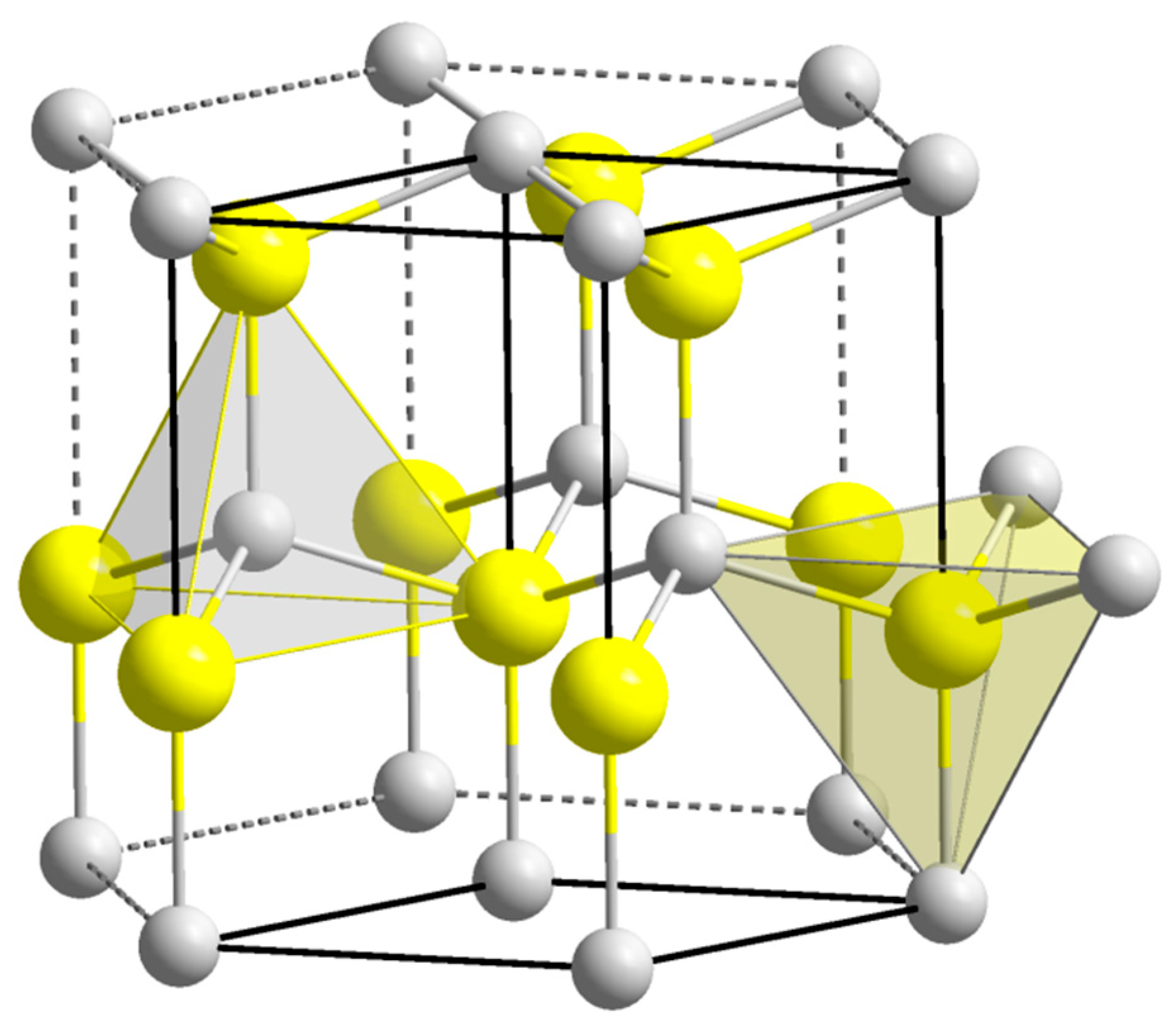
ZnO is a direct wide band gap semiconductor (EG = 3.37 eV [22]) transparent in the visible wavelength range and suitable for UV and blue wavelength optoelectronic applications with a large exciton binding energy of 60 meV [23] enabling efficient excitonic emission at room temperature. A low refractive index of 2.05 enables easier light extraction from an optical device. Its wurtzite crystalline structure with the lattice parameters a and c equal to 3.2495 Å and 5.2062 Å [24], respectively and the large piezoelectric constants enable strong piezoelectric polarization in the material, resulting not only in the possibility of piezoelectronic device fabrication but also the fabrication of high quality 2D electron gas structures [25,26] with the recent observation of fractional quantum Hall effect [27]. From a more chemical point of view, the lattice can be described as two intertwined hexagonal close packed Zn and O lattices, arranged in such a way that each Zn2+ ion is coordinated by four O2- ions in a tetrahedral arrangement and likewise, each O2− ion is coordinated by four Zn2+ ions in the same way (see Figure 1). The bonds are sp3 hybridized bonds of almost equally ionic and covalent character. It has to be said here that, under special growth conditions, or using cubic lattice substrates, ZnO can form zinc blende lattice films with the same ionic coordination types, however since these are fringe studies in the field they will not be discussed here. Additionally, ZnO forms ternary wurtzite alloys with CdO and MgO making possible band gap engineering of the material [28] with the band gap widths from 2.3 eV [29] to 4.0 eV [30] enabling the growth of high-quality quantum well structures [31,32] (see Figure 2).
The unique optical and piezoelectric properties of ZnO are paired with its nontrivial electrical characteristics. A II-IV semiconductor, ZnO is usually reported to exhibit n-type conductivity with high carrier mobilities in the range of 100 cm2V−1s−1, even when not intentionally doped. Although the first reports explained that defects, such as Zn interstitials (Zni) or O vacancies (Ov), were responsible for the intrinsic n-type of the material [34,35], more contemporary works [36,37] argue that Ov are deep donors which cannot be responsible for the n-type conductivity and that Zni although being shallow donors, have large formation energies and diffuse fast, thus being unstable. Znv are deep acceptors with low formation energies under the conditions leading to n-type ZnO growth and can therefore compensate the n-type charges [38,39,40]. Finally, Oi and oxygen and zinc antisites are regarded as having too large formation energies to exist in significant concentrations in the material [41]. There has been a consensus therefore, that the intrinsic n-type conductivity of ZnO films is due to impurities present during the growth process. Depending on the growth process, hydrogen, fluorine or group III impurities (In, Ga, B, Al) have been taken into account. As far as these group III impurities are concerned, all of them have been found to intentionally dope ZnO into n-type [42,43,44,45] by Zn substitution. Al-doped ZnO is commercially successful as a transparent conducting film for transparent electronic applications [46]. Fluorine substituting oxygen in the lattice acts as a shallow donor with an ionization energy of 80 meV and low formation energy [47]. Finally, hydrogen was found to be acting as a shallow donor with 35 meV ionization energy [48] at the interstitial position. Unlike as in other semiconductors, where the hydrogen interstitial is an amphoteric dopant [49], incorporating into n-type material as an acceptor and into p-type as a donor, in ZnO it always incorporates as a shallow donor [50]. Hydrogen substituting oxygen is also a shallow donor with a slightly lower formation energy than Hi [38,39,40,41,42,43,44]. It has to be underlined here, that while Al and In impurities may mostly incorporate during chemical crystal growth, hydrogen impurity may be relevant for vacuum-based techniques, as most vacuum chambers are machined out of stainless steel, which is known to outgas hydrogen [51,52]. However, it has to be noted that the community dealing with ZnO materials still seems to not put enough attention to the recent developments of the defect level identification. This is especially common when describing the green luminescence band, visible in most ZnO materials. Some authors focused most on the fabrication and application of the given sample, claim it to be related to Znv and some to Ov based solely on literature references, not on experimental considerations. However, the bulk of the literature finds works contradicting themselves, when applied to ZnO as a whole, not to the particular case of ZnO structure using a particular technique under the particular conditions. Recent experimental investigations show that in fact the green luminescence can originate from various sources, even in the same sample – e.g., for hydrothermal ZnO single crystals both Znv coupled with H+ and Ov have been reported to give rise to the green luminescence with small offsets [53].
ZnO is composed of very chemically active ions, resulting in a material being itself far from inert. Firstly, it lends itself easily to wet chemical etching, which simplifies epitaxial device processing down to micron scale. But this reactivity is also beneficial from the material fabrication point of view, as ZnO easily forms precipitates in solutions, and based on the conditions of the reaction a plethora of morphologies is attainable, including nanocolumns [54], nanowires [55], nanosheets [56], nanofibers [57], nanoflowers [58], nanoparticles [59], and quantum dots [60], as well as 3D hierarchical architectures [61], which is one of the reasons for the incredible popularity of ZnO nanostructures in research. As an example, Ko et al. reported on the fabrication of a hierarchical ZnO nanoforest using hydrothermal growth [62] and Wang described the growth of nanowires, nanotubes, nanobelts, nanohelixes, nanocombs, nanorings, nanopropellers, nanosprings, and nanoshells using ZnO powder sublimation and deposition [63]. Additionally, porous ZnO was developed using nanotube membranes [64] and dynamic template assisted electrodeposition [65]. Due to their high surface-to-volume ratio and surface reactivity, these structures are regarded as potential candidates for particle absorption applications, be it photons in dye-sensitized solar cells [61] or bio-chemical molecules in biomedical sensors [66] or gas molecules in gas sensors. Additionally, its low toxicity, biocompatibility and biodegradability make ZnO nanostructures and nanoparticles a material of interest in biomedical and environmental systems. However, care has to be taken when using ZnO nanostructures in aqueous environments, since at low concentrations ZnO dissolves in water and the dissolution concentration threshold increases rapidly with decreasing pH, potentially forming many problems for real life, stable applications in areas such as biomedicine or photocatalysis. In such cases, the appropriate structure and morphology design, sometimes additionally employing ultrathin surface passivation layers, can be viable solutions. Noteworthy is the fact that, contrary to high quality ZnO epitaxial and thin film growth where vacuum-based techniques are most often employed, nanostructured ZnO is in most cases grown using chemical methods, with only a few developments based on vacuum techniques such as magnetron sputtering (MS) [67] or pulsed laser deposition (PLD) [53]. The chemical methods, although relatively economical and easy to implement, may meet with challenges in the areas of large-scale production, uniformity, and replicability when deployed, not as kg and larger-scale powders, but in the forms of mg and lower-scale doses or thick films.
Other, less known properties of ZnO include high radiation hardness, high thermal conductivity, and strong non-linear optical behavior, which makes the material interesting, respectively, for space applications, thermoelectric generators, and nonlinear optical elements.
One of the biggest unsolved challenges in the technology of ZnO is the fabrication of stable p-type ZnO material, e.g,. for homojunction applications in LEDs or laser diodes (LDs) but also for a variety of bipolar electronic devices. Such materials not only have to exhibit stable transport properties, but also be preferentially of high crystalline quality, devoid of grain boundary acceptor aggregation/segregation as well as with low density of non-radiative recombination centers. There have been many potential candidates for acceptors in ZnO, including elements from group IA, IB and V but so far, no commercially adopted breakthrough has been reported.
3. Methods of Fabrication
ZnO can be grown as large-scale single crystals, epitaxial structures, thin and thick film structures as well as nanostructures and nanoparticles. The methods of fabrication are as widespread as the reported structures and their applications. The methods are usually chosen based on their typical intrinsic possibilities and limitations to grow a given type of a structure, with some reports pushing the conventional capabilities of growth to obtain atypical structures.
3.1. Bulk Crystals
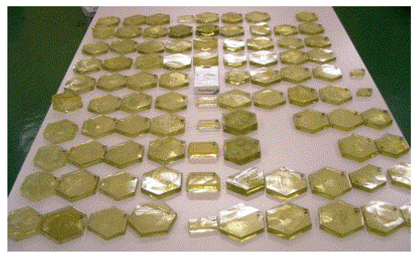
The dominant method of fabrication for bulk single crystal ZnO is hydrothermal growth [68], but the feat is also realized using vapor growth [69] and solution growth techniques. Crystal growth in the hydrothermal method occurs in a water-based solution, under a temperature gradient and high pressure. The high pressure (15–150 MPa) is needed for the dissolution of the crystal starting materials in a lower temperature (<500 °C) than in the case of ambient pressure. Due to the harsh conditions the process is performed in an autoclave. The starting materials are a nutrient (here ZnO powder) and water with additions of alkaline mineralizers for raising the nutrient concentration in the solution to a preferred range, usually around 5 wt.%. In the higher temperature part of the autoclave, the nutrient dissolves in the now supercritical water under the elevated pressure and the constituents are transported to the lower temperature part where growth occurs on a starting seed crystal. The method is well developed commercially, and the available single crystals have diameters as high as 75 mm (see Figure 3), with very low dislocation densities (<100 cm−2), good flatness, and low impurity concentrations. The crystals have electron conductivity and can be made semi-insulating by doping with Li or N acceptors from the mineralizers during growth [70]. Such crystals form a good substrate not only for the homoepitaxy of ZnO-based structures, but also due to a low lattice mismatch with GaN (1.8%), they could well accommodate GaN-based structures. The current trends in research on the hydrothermal growth of ZnO bulk crystals are the identification of the defect-related luminescence, surface properties and studies on dopant indiffusion.
3.2. Epitaxial Films
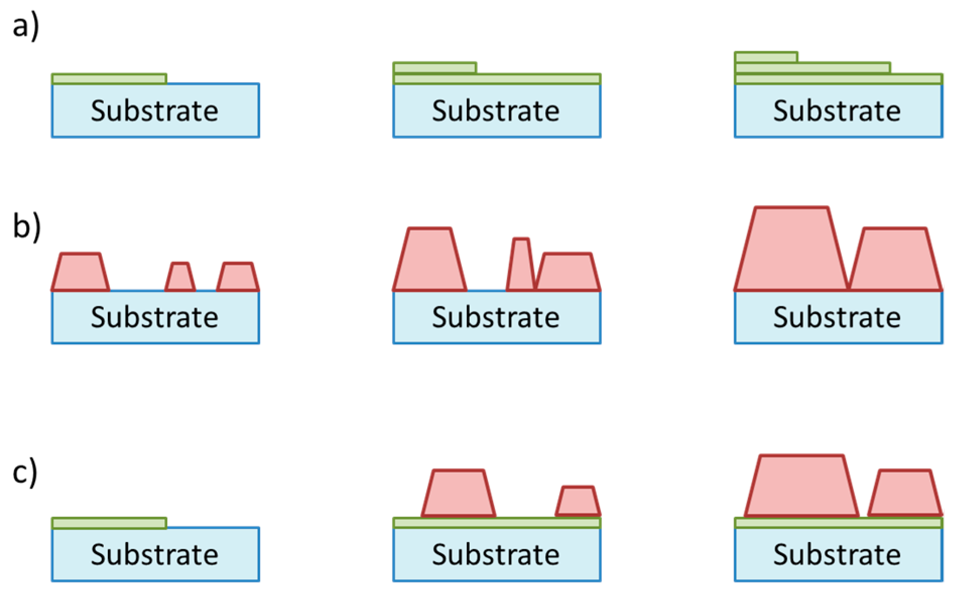
Moving on to the fabrication of structures typical for the physical and electronic engineering worlds, epitaxial structures of ZnO and related materials have been grown using molecular beam epitaxy (MBE) [71], in particular the plasma-assisted version (PA-MBE) [72,73] due to the need for active oxygen during growth, as well as metalorganic chemical vapor deposition (MOCVD). The PA-MBE method utilizes an ultra-high vacuum (10−8 to 10−12 Torr) reaction chamber and ultrapure elements (99.999% to 99.99999% pure), which are both needed to maintain the low background impurity concentration at the low physical deposition rate allowing epitaxial growth. In the case of ZnO, the Zn sits in a crucible which is heated to produce an outward flux of Zn atoms, while the O is generated from a form a remote oxygen plasma. By controlling the partial pressures of both species at the substrate, as well as the temperature of the substrate itself, a variety of epitaxial growth modes can be achieved, from step-flow epitaxial growth to Stransky-Krastanov quantum dot/nanoparticle growth mode (see Figure 4). The growth can be monitored by a set of tools, the most common of which is the RHEED (reflection high-energy electron diffraction) monitoring the surface of the growing materials, enabling the control of the growth mode. The MOCVD technique [74] on the other hand is performed in an ultrapure gas flow at moderate pressures of the order 10 to 1000 Torr and uses surface chemical reactions between the elemental precursors to control the monolayer growth. The precursors used for the growth of ZnO are organometallic Zn compounds such as dimethylzinc (DMZ) or diethylzinc (DEZ) and pure oxygen or water for the O and their partial pressures and the substrate temperature again play a decisive role in the properties of the resulting structures. These methods utilize costly and complicated equipment, very high purity elemental sources and high growth temperatures, typically around 550 °C for pure ZnO, to provide the highest quality epitaxial structures with well controlled thickness, composition, as well as impurity and dopant levels. Band-engineered films and quantum structures can also be developed using these techniques. Some reports were provided on PLD [75] and MS [76] growth of epitaxial ZnO structures, however these techniques are not common for the task due to the difficulty in controlling the epitaxial growth conditions and impurity levels in such reactors. Recently, the epitaxial ZnO structure growing community has been focused on achieving the highest crystalline quality of the films, obtaining stable and repeatable p-type doping, as well as studies of physical optical phenomena in quantum structures of ZnO, ZnMgO, and ZnCoO.
3.3. Thin Films
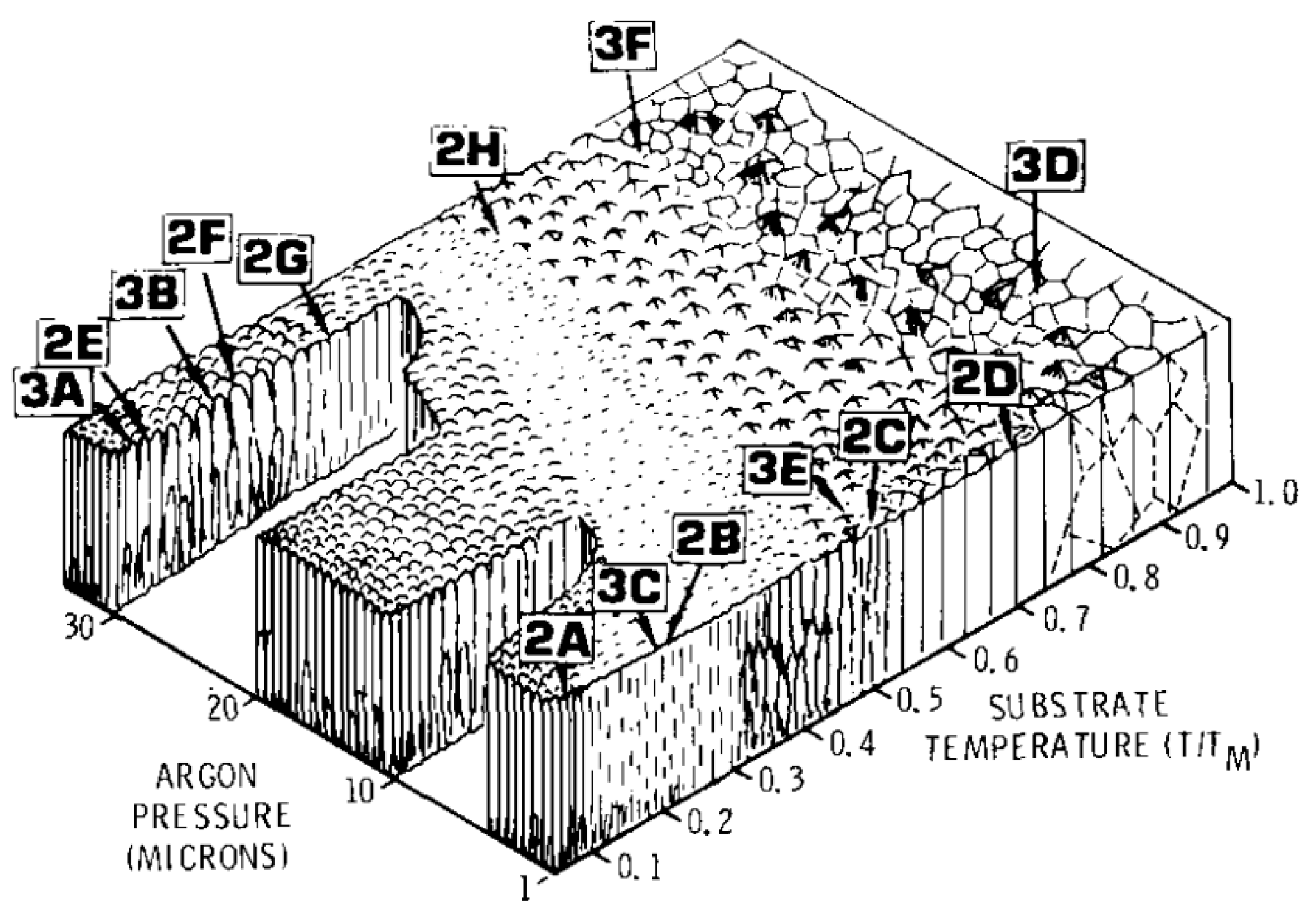
Thin ZnO films (several nm to a couple micron) are mostly developed using pulsed laser deposition (PLD), magnetron sputtering (MS), or atomic layer deposition (ALD) and their morphologies are usually polycrystalline and follow those described by the Thornton zone model (see Figure 5). Pulsed laser deposition [77] is a vacuum technique, in which a pulsed high-power laser beam is focused on the target material leading to its instantaneous local heating and ablation/evaporation resulting in its deposition on the substrate. For ZnO, the target is either Zn or ZnO and oxygen can be added into the chamber to oxidize the growing film. The density of the nucleation sites during evaporation is very high, much higher than in the case of MBE or MS causing a smoother film growth. With substrate heating (usually around 350 °C), PLD enables step flow and epitaxial growth, however since the majority of work on epitaxial ZnO is currently done by PA-MBE and MOCVD, PLD has seen interest in non-epitaxial, thin film growth of ZnO. An advantage of this technique is the relatively short process time, the downturn would be in the throughput with limited target and substrate areas feasible. MS [78] on the other hand is a technique known for it’s ease of upscaling from lab to production scales by increasing the dimensions of the chamber and the used targets. The targets are the source material to be deposited, usually with a purity of 99.99% and for ZnO the material used is either Zn or ZnO. The sputtering process takes place in an initially evacuated vacuum chamber (10−6–10−8 Torr) where Ar gas is introduced with O2 gas as the reactive gas, if needed. A voltage around 100V is put between the target and the substrate creating cascade gas ionization (plasma) leading to bombardment of the target surface and ejecting or sputtering away the target material onto all surfaces in the chamber, including the substrate. Usually, thin ZnO films are deposited on unheated substrates, but for higher quality films, substrate heating can be applied around 300–550 °C [79]. The advantage of sputtering lies in the large-scale uniformity, good microstructure, as well as thickness control and repeatability of the deposited films. Additionally, this technique can be directly used with lift-off photolithography patterning, when the deposition is done at RT, significantly simplifying device processing using the deposited films. The ALD technique is the third commonly used one for depositing ZnO thin films and unlike the two previous ones, it is a chemical deposition technique similar to MOCVD. Like the latter, it also uses molecular precursors of zinc (DMZ or DEZ) and water or ozone for the oxygen, however the process conditions and especially the substrate temperature are chosen so that the chemisorption of the molecules is promoted while physisorption is much less probable. When performed with strict precision, this technique can result in layer by layer growth of Zn and O monolayers [80]. However, practice shows that most works focus on polycrystalline thin film growth of ZnO [81]. The advantages of the ALD technique are the following: a deposition temperature as low as 100 °C, possibility of large-area deposition, and a conformal coverage of all shapes and protrusions on all exposed surfaces of the substrate making it useful for encapsulation-like applications. A significant amount of work on the doping of ZnO has been done by means of MS and ALD due to the relative ease of dopant addition to the deposition process. In MS it can be either by sputtering from a pre-doped target, co-sputtering the dopant alongside ZnO or doping from the gas phase, e.g., with nitrogen [82]. For ALD, the dopant would be added from another precursor in its own monolayer deposition cycle, reaching the desired concentration [83].
The techniques described up to now are well-established high maintenance and relatively high complexity techniques, requiring dedicated and usually costly equipment. Their advantage is in the multifunctional control of the growth process as well as in the available high purity materials for the growth which is of high importance for any electronic applications.
The following typically chemical thin film growth techniques, although significantly easier to prepare and much less cost-intensive, can be a priori used with any grade of starting material or solvent, which puts an even larger burden on the experimentalist to execute the experiment with the required level of control of the purity and non-intentional doping, which is especially important in the case of such a material as ZnO. One of the more straightforward techniques is sol-gel deposition [84,85]. A colloidal particle suspension is prepared by means of mixing selected precursors in a solvent with a stabilizer and is subsequently spin coated on the selected substrate. For ZnO, usual Zn precursors are acetate, nitrate or perchlorate. The solvent is usually an alcohol with a low C-number. The stabilizer added to the mixture is most usually an amine such as monoethanolamine (MEA). The whole solution is stirred in a bath at a temperature usually within the range RT−80 °C until a homogeneous sol forms. After ageing and spin-coating, the films undergo several drying and annealing steps at temperatures from 100 °C to around 500 °C, forming the final film. The spinning and drying steps can be repeated. Dopants can be added as other metallic precursors. Another relatively popular thin ZnO film deposition technique is spray pyrolysis [86]. In this technique a spray of a precursor solution, similar to that of the sol-gel is jetted using a carrier gas in the direction of a heated substrate. For ZnO, Zn acetate or nitrate is used with water or an alcoholic solvent and the substrate temperature around 400 °C. A technique utilizing the same precursors, stabilizers and solvents that has recently seen a rise in interest is inkjet printing [87]. Here, an ink is formulated using the three materials and is then jetted in the previously designed shapes onto a substrate. Subsequent annealing similar as the one applied before, leads to solvent evaporation and film formation. A variation of the ink-jet technique utilizes nanoparticle dispersions as the ink that coalesce in the printed pattern after annealing. One advantage of the printed approach is the direct writing capability, simplifying device processing. Care has to be taken however when formulating inks to allow for good wetting and coalescence at the same time retaining high jetting resolution and appropriate flow characteristics on the substrate during drying. The final thin film deposition technique described is electrodeposition [88]. It can only be used to coat substrates that are conducting or covered with a conducting film. A common research substrate is glass pre-coated with an indium tin oxide (ITO) conducting thin film. The substrate being the working electrode is immersed in a solution of a zinc salt in a solvent heated above 50 °C, usually zinc acetate or nitrate in water. A counter electrode is also immersed in the solution to close the circuit, a reference electrode is added for potential reference and an electric current is fed between the anode and the cathode through the solution resulting in a mass transfer of the Zn2+ ions to the working electrode and an evolution of hydroxide ions from the solution at that electrode as well leading to the formation of zinc hydroxide at its surface. The elevated temperature of the solution is needed for the final dehydration of zinc hydroxide into ZnO and water. The process is fast and allows the coating of complex geometries on large-scale substrates beneficial in applications like photocatalysis.
ZnO thin film growth is a branch of ZnO research that has been recently most focused on the band gap and electronic states’ engineering, the use of ZnO as transparent conducting oxides, their use as optical coatings, e.g., in solar cells as well as to a lesser extent transistor-based devices and the problems of p-type doping.
3.4. Thick Films
Thick films are usually considered as films of a thickness greater than 10 micrometers. Screen printing is the dominant technique for thick film fabrication, with electrodeposition, sol-gel deposition and nanoparticle aggregation methods also used.
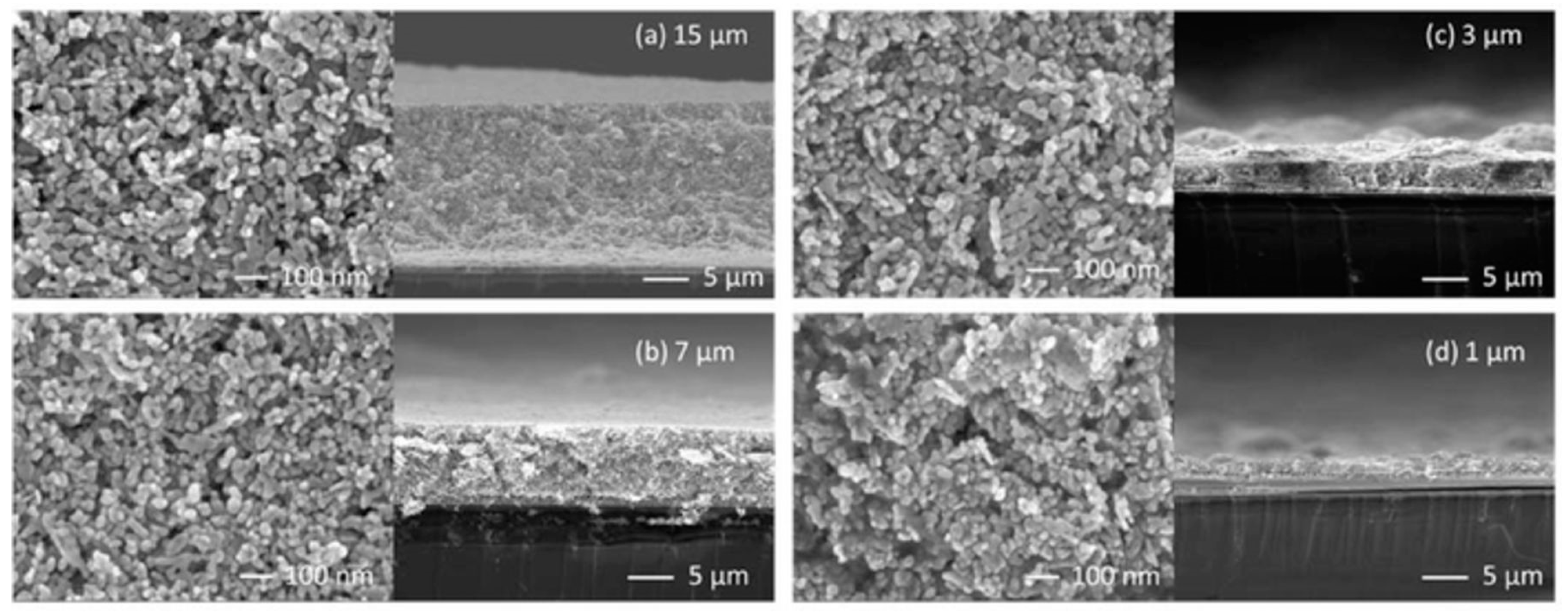
Screen printing of thick ZnO films [89] uses the starting material in the form of a paste made up of ZnO powder with a solvent and a polymeric binder (e.g., polyvinyl alcohol or ethyl cellulose). The paste is put on a mesh with a pre-patterned stencil, both lying on the substrate. The paste is then moved along the mesh using a doctor blade and contacts the substrate in the openings of the stencil. After the mesh and stencil are separated from the substrate, the fabricated thick film patterns are dried around 100 °C and subsequently sintered (‘fired’) at around 500 °C to remove the organic components and fabricate continuous films, often called ‘ceramics’. These materials are characterized by a not-dense, porous morphology irrelevant of the obtained thickness (see Figure 6). The sol-gel thick films are fabricated either by multiple spin-coating steps as described above or by dip-coating [90]. For electrodeposition, a longer deposition time is applied to obtain thick films. ZnO thick films deposition is an established technology with few new developments reported recently, and its main focus is on varistors and gas sensors using screen printing.
3.5. Nanostructures and Nanoparticles
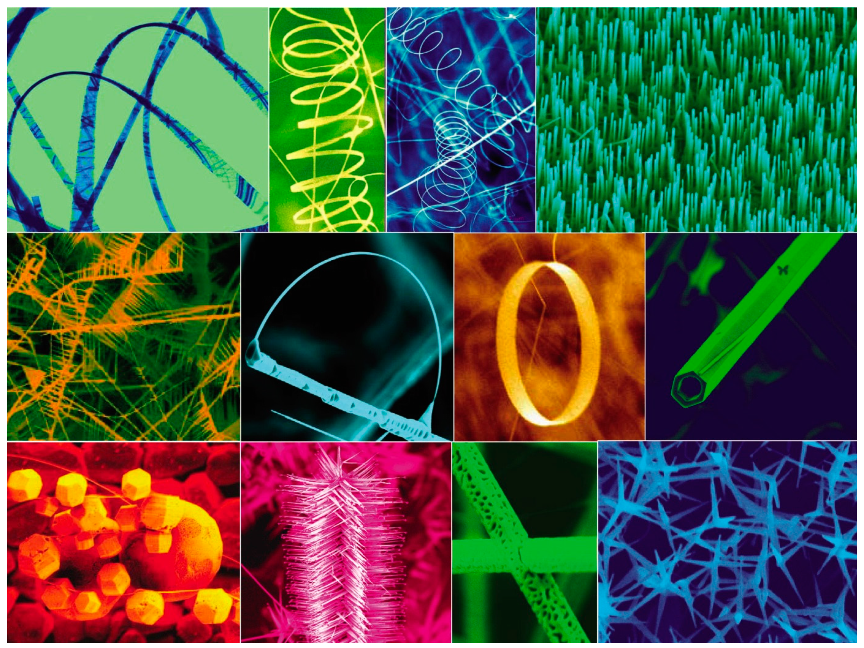
Nanostructures form the bulk of modern ZnO research trends due to their ease of fabrication using a wide array of methods enabling the fabrication of nanostructures with many shapes and sizes. Nanospheres [91], nanoplates [92], nanorods [93], nanotubes [94], nanoneedles [95], nanoribbons [96], nanobelts [97], nanosheets [98], nanotrees [99], nanodendrites [100], nanoflowers [101], nanoshells [102], nanocorals [103], nanovolcanoes [104], nanopyramids [105], nanocolumns [106], nanotowers [107], nanocombs [108], nanorings [109], nanosprings [110], nanowires [111], nanocages [112], nanopencils, nano-pin-cushion cactus [113], and more are all achievable, and the names describe their morphology as a nanoscale version of human-perceivable shapes (see Figure 7). Most of the reports on ZnO nanostructure formation in the literature are based on the chemical synthesis approach where Zn salts (acetate, nitrate, etc.) are combined with bases to initiate a reaction leading to zinc hydroxide formation. Said hydroxide is then oxidized thermally to create ZnO. The reaction usually occurs in a solvent and the products can be collected as a powder or adsorbed onto a substrate. The previously described sol-gel and spray pyrolysis methods are particular examples of this approach that can be adopted to growing nanostructures by appropriately controlling the parameters of the solution and drying. Solvent precipitation or solvothermal methods are very common to grow nanostructure powders. Here, the metal salt is put in a solvent, usually with the addition of a compound with the OH group (base, alcohol etc.) or with water [114] as the other reactant leading to zinc-hydroxide complex formation (precipitation). The whole reaction can be heated in an external bath (solvothermal) and sometimes under reflux to tune the reaction conditions. By controlling the type of reactants [115], temperature [116], alkalinity [117] and type of solvent and its water content [118], different morphologies can be obtained of the nanostructures. A variation of the solvothermal technique when the solvent is water is commonly called hydrothermal technique, which should not be confused with the embodiment of the hydrothermal technique described in the section on bulk ZnO growth due to the absence of high pressures and autoclaves as well as the precursors being zinc salts, not ZnO. Depending on the embodiment of the applied technique, the nanoparticles may need to undergo a final calcination step to fully turn to ZnO [119]. Further changes can be done by exchanging thermal heating to microwave heating in an embodiment called microwave solvothermal (hydrothermal) synthesis. The main advantage of this technique is in the higher efficiency of heating using microwaves than in the case of conventional heat transfer through conduction and convection while keeping higher uniformity and shorter reaction times [120]. Sonochemical synthesis is another variation of the solvothermal method of ZnO nanostructure formation that utilizes ultrasound mixing of the constituents of a typical solvothermal solution through bubble formation and cavitation [121]. It should be noted here that the ultrasonic deposition of nanostructures from a nanoparticle sediment is also used, where the ultrasound electrode is shaped and placed in a manner allowing the cavitation of bubbles to be used as a jetting medium for ZnO nanoparticles suspended in the working liquid. The jet drives the nanoparticles to a substrate placed at the bottom thus forming a nanostructured film [122]. Electrospinning has been shown as an effective technique for the fabrication of ZnO nanofibers. The starting material is a solution of the ZnO precursor and a polymer in a solvent. Said solution is fed through a needle and a charged thread is drawn from the meniscus in the needle upon applying an electric field. The material has a very high aspect ratio and requires calcination to form polycrystalline ZnO fibers at 300–600 °C [123]. A similar technique, extrusion dripping is a new approach to form spherical monodisperse ZnO nanoparticles, where the working precursor solution is controllable dripped from a needle into a stabilizing polymer solution. After washing, the powders are calcinated at around 500 °C [124]. Another known technique for the preparation of nanopowders of ZnO is mechanochemical synthesis. It is characterized by solid-state reaction of precursors during long-term mechanical grinding in a ball mill. The advantage of this technique is the low temperature of reaction and almost no chemical equipment needed, but the scale of the fabrication is rather low. Here, Zn salts and hydroxyl or carboxyl group containing compounds are usually chosen as the precursors. The powders can be additionally calcinated if the constituents require so and the impurities are removed by washing [125]. Pure and doped ZnO powders have also been prepared by means of combustion synthesis. Here the cation precursors are metal salts (e.g., nitrates) and fuel (e.g., urea). After ignition at around 500 °C the salts are oxidized and a very fine nanopowder is created [126]. A significant aspect of nanoparticle/nanopowder synthesis has to be in their stability [127] and agglomeration management. Since for most applications, the nanoparticles should be not agglomerated, the stabilization of ZnO nanoparticle suspensions is key, either by capping ligands or polymer shells [128]. To avoid agglomeration, complex nanostructures can also be formed by grafting the ZnO nanoparticles on polymers [129,130,131] either through surface modifications and cross-linking of modified nanoparticles or by methods binding the nanoparticles onto a polymeric template. Another route of high surface area ZnO nanostructure formation is the pyrolysis of Zn-containing metal-organic frameworks (MOFs), where highly porous MOF templates are synthesized solvothermally as described above and subsequently slowly pyrolyzed at 450 °C to form ZnO nanocages [112].
In addition to the chemical synthesis routes, physical methods are used successfully for nanostructure fabrication. The most straightforward way to make zinc nanostructures is to oxidize zinc metal. Even a controlled oxidation of appropriately deposited zinc templates can yield high aspect ratio crystalline ZnO whiskers or nanowires [132]. Another simple technique with significant success in fabricating ZnO nanostructures, especially nanowires, is the vapor transport technique, where the zinc powder is vaporized in an evacuated quartz tube around 500 °C and the Zn vapor is transported by carrier gas to a lower temperature region where the growth occurs on substrates through condensation in the presence of oxygen [133]. The growth is controlled by the flow rate, pressure in the tube and the temperature of the condensation region. A simple and relatively fast technique, the scale up of which is however limited by the internal diameter of the quartz tube and the radial temperature gradients within. The substrate size problem can be however circumvented when flexible substrates are used for the condensation. ZnO nanostructures can also be grown using thermal evaporation of solid ZnO powders [134,135]. This technique is similar to the vapor transport approach and utilizes a quartz tube reactor. However, the starting material is ZnO and due to this, the temperature in the tube has to be much higher, around 1100 °C. There is however no base vacuum nor carrier gas needed. The source material is deposited on the walls of the reactor or on the inserted substrates and therefore the approach faces similar scale-up problems as the vapor transport technique with additional concerns of the thermal stability of the used substrates. Although PLD and magnetron sputtering have been used mostly for thin film and epitaxial ZnO growth, there are reports on nanostructure formation using these approaches. It was shown that, using low pulse energies in PLD with a ZnO target, nanorods can be grown on sapphire substrates [54]. MS has shown to be useful for the growth of developed nanocoral hierarchical morphologies where the initial deposited structures are Zn and have to be thermally oxidized at 400 °C to form ZnO. The deposition was done using a metallic zinc target in a low pressure [67]. Additional report shows that by tuning the gas flow parameters, ZnO nanocolumns can be grown at room temperature using MS [136]. Other reports on MS growth of ZnO nanostructures utilize either pre-patterned templates that are overcoated by ZnO films [137], a thermally-induced formation of the nanocolumns due to lower adatom coalescence during film growth at certain temperatures [138] or they use catalyst beads to induce the vapor-liquid solid approach (VLS) [139]. The VLS approach has been commonly used to obtain semiconductor nanowires with MBE and MOCVD. It is a catalyst-based approach where a gold coated substrate is first pretreated so that nm-scale gold beads form on it. During growth, these beads transform into droplets of an Au/Zn eutectic. The material growth is facilitated directly under the droplet leading to formation of nanowires with the eutectic caps. ZnO nanowires and nanobelts have been shown to be grown this way using MBE [140,141] and MOCVD [142]. Catalyst-free nanowire growth has also been shown using very thin ZnO buffer layers, which removes gold contamination from the nanowires [143]. ALD has been also used to grown ZnO nanowires using gold catalyst [144]. An interesting technique for ZnO nanostructure deposition is the low-energy cluster beam deposition technique (LECBD). The technique uses a gas-aggregation source to form clusters of the material that will be deposited on the substrate, in this case ZnO nanoparticles. The material source is either a sputtered target or a target hit by an impulse laser, akin to the PLD approach, and the cluster size is determined by the pressure of the buffer gas in the formation chamber. On the way to the substrate the particles are formed by the interaction with one another in the presence of the buffer gas and the beam is conditioned by appropriate nozzles [145]. ZnO nanoparticles with several nm diameter can be deposited this way using a ZnO target, either as a continuous thin film or as for decoration of other materials [146]. With so many different techniques, and a material very sensitive to the fabrication conditions, the array of reported nanostructures is massive, and their properties differ significantly from report to report. Even with the same morphology class (e.g., nanoflowers) but different approaches to fabrication, the nanostructure properties can differ due to different levels of background impurities. This, on one hand, showcases the wide possibilities of ZnO applications and, on the other, limits the reproducibility and development of the knowledge on ZnO and requires the researchers to have a significant understanding of their experiments, the purity of their experimental environment as well as the field in general.
The current topics in the area of ZnO nanostructures are related mostly to their applications in photocatalysis and gas sensing with additional focus on biochemical sensing application with less emphasis on new fabrication approaches themselves. Additionally, magnetic doping in ZnO nanostructures is still explored.
To summarize, based on the review of the fabrication techniques it can be seen that a general division into more physical and more chemical methods is present. The former ones are mostly used for epitaxial structure and thin film growth and are characterized by higher complexity, high purity and dopant control and are mostly related to basic research on the properties of ZnO and its structures and on overcoming the p-type doping challenge. The starting materials for the synthesis include elemental Zn and ZnO as well as oxygen. Some of the chemical methods are also used for the epitaxial structure synthesis (MOCVD) and thin film deposition (ALD) and utilize the reactions between Zn metalorganic precursors and water or ozone, but the vast majority of the chemical methods is applied for the fabrication of nanoparticles/nanostructures and is based on Zn salts (acetate, nitrate, chloride etc.) reacting with OH groups from appropriate bases in the presence of various solvents to form nanostructures in solution or in suspension. The final product is obtained either by washing and drying, or by coating on a substrate and annealing. Especially due to the difficulty in obtaining stable p-type behavior in ZnO, the research in the physical groups has slowly been dying down with several highly focused groups still pursuing the ultimate goal of truly p-type ZnO and the rest working to utilize the n-type ZnO of high quality. In the realm of nanostructures however, the chemical synthesis of ZnO is constantly gaining momentum due to the wide possibilities of synthesis and the very exciting applications close to the chemical and biochemical device industries.
4. Review of Applications
Having presented a review of the fabrication techniques for different ZnO structures, this part of the paper will go through the different existing and perceived applications of the material to give a complete overview of the material’s potential. The division will be again based on the type of the structure: epitaxial, thin film, thick film or nanostructure.
4.1. Epitaxial Structures
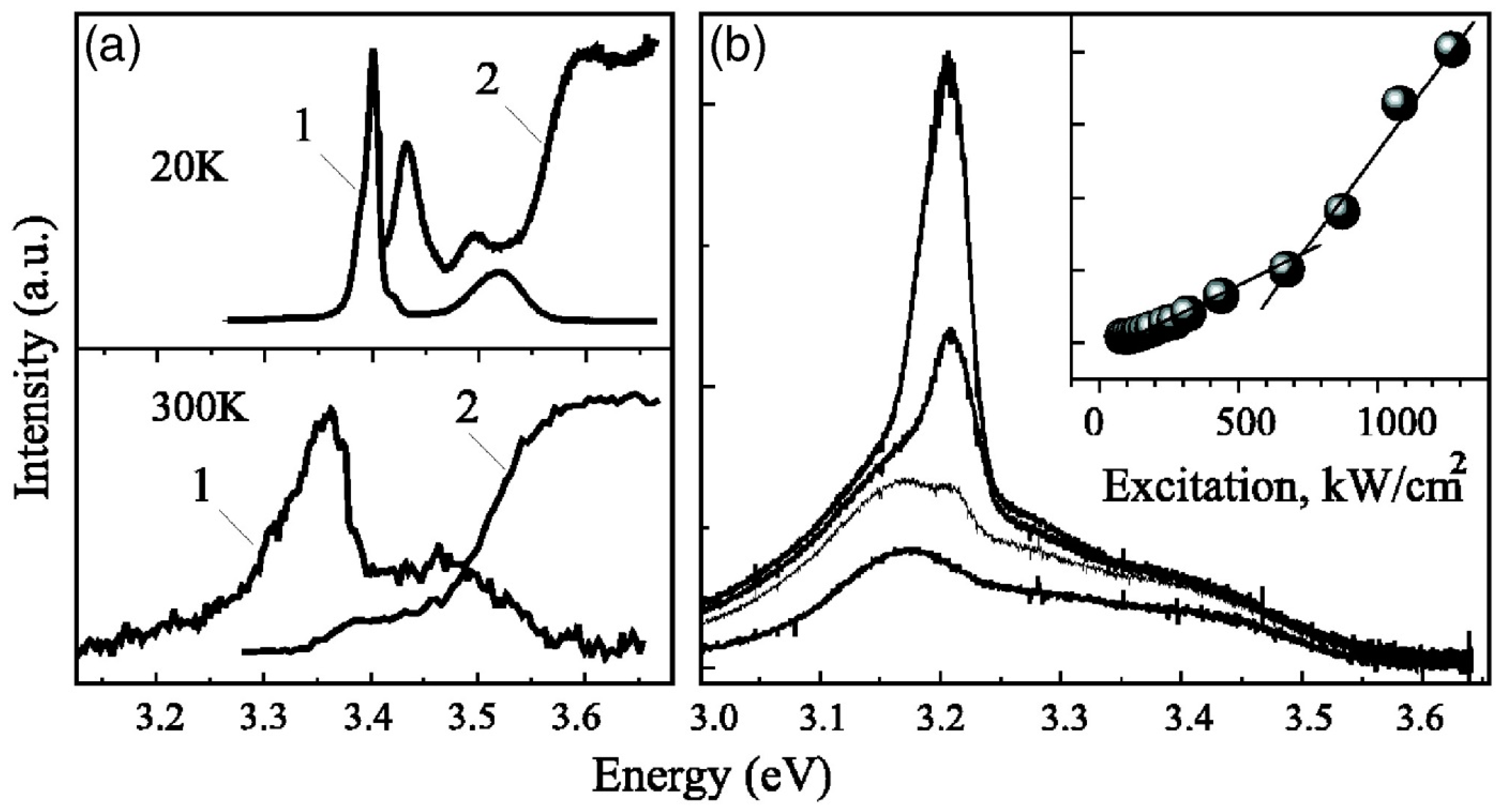
The effort into obtaining stable p-type material is intensive but still inconclusive, as discussed further in the manuscript, therefore the epitaxial ZnO devices studied are either unipolar od grown on p-GaN templates. However, the performance of the latter is not better than in the case of fully GaN structures. Therefore, this text will focus only on purely ZnO devices. The substrates of choice for epitaxial growth are either the popular but lattice mismatched sapphire or the lattice matched ScAlMgO4 with less works on ZnO bulk substrates. The bandgap engineering of ZnO enables quantum structures to be formed making use either of the built-in piezoelectronic polarization creating a two-dimensional electron gas (2DEG) at the interface between ZnO and ZnMgO or the common quantum well structures towards optically pumped light emitters. The structural quality of the structures is very high, evidencing good maturity of epitaxial ZnO growth with an observation of both integer [25] and fractional [147] quantum Hall effects in ZnO/ZnMgO structures with low temperature electron mobility exceeding 180 000 cm2V−1s−1. ZnO/ZnMgO field effect transistors (FET) with the 2DEG channel have been reported with a 1.75 GHz cutoff frequency with a room temperature mobility of 165 cm2V-1s-1, about an order of magnitude lower than for their AlGaN/GaN counterparts [148,149]. Optically pumped UV lasers have been demonstrated using ZnMgO/ZnO heterostructures [150] (see Figure 8). and calculations show that, if realized, ZnMgO/ZnO room temperature quantum cascade lasers would have double the efficiency of AlGaN/GaN devices with the same architecture [151]. At the time however, these devices are more used for fundamental studies and cannot achieve maturity and compete with the AlGaN/GaN technology.
4.2. Thin Films
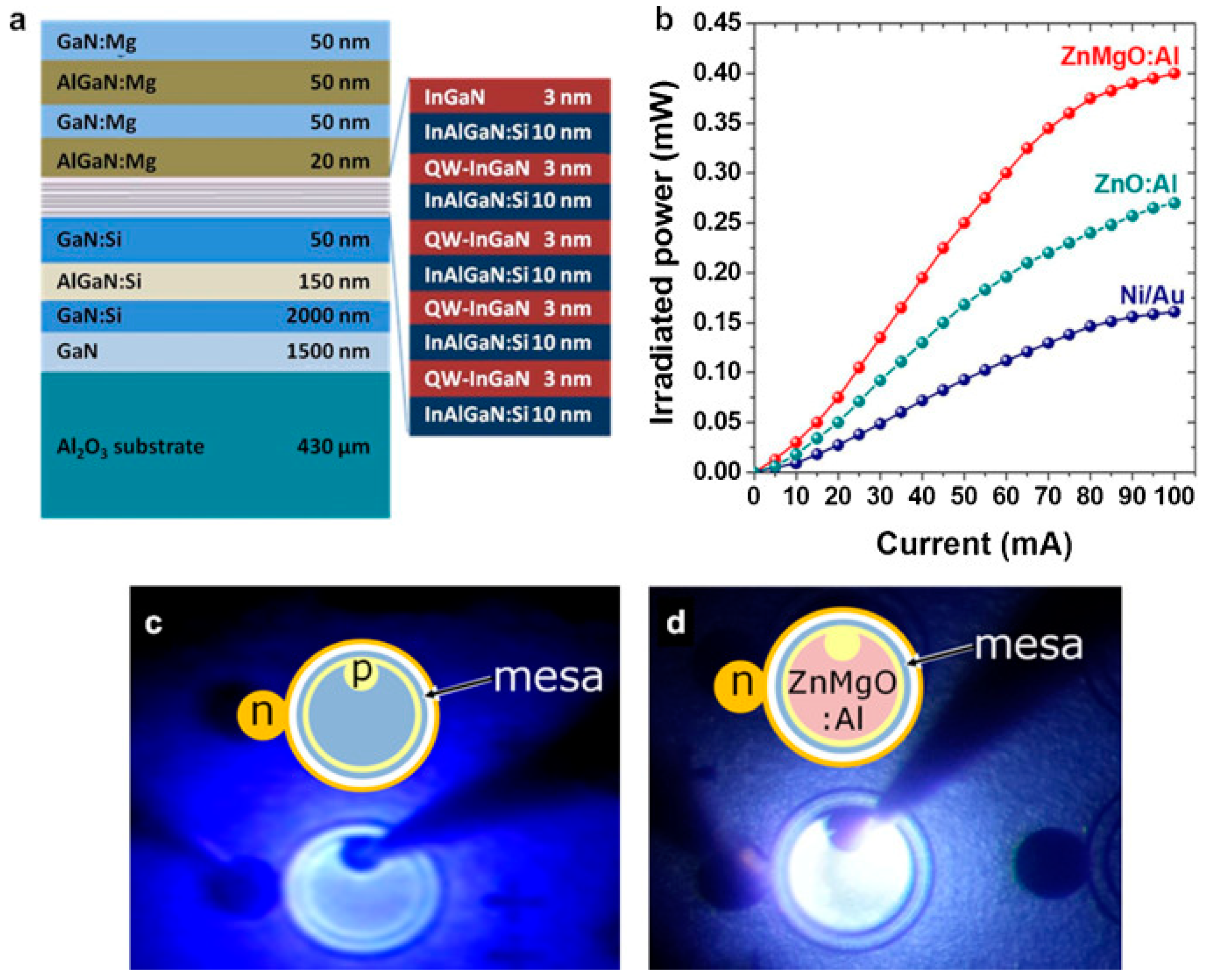
The applications of thin film ZnO are related to the large-scale deposition required and the basic electrical and optical properties—therefore, the biggest areas of industrial interest lie in the n-type ZnO:Al (AZO) for transparent electrodes as well as in optical antireflective coatings. While p-type doping is a big hurdle for ZnO, n-type high efficiency doping is one of its strengths. With the rapid development of solid-state lighting, photovoltaics, touch-screens and all technologies requiring one or more parts of the active device part to be transparent, the market for transparent electrodes has been steadily growing and offers an opportunity for ZnO:Al breakthrough. AZO has specific benefits over the commonly used transparent electrode of indium tin oxide (ITO), such as a composition made of abundant materials, controllable doping level and bandgap engineering possibilities that make it, in principle more flexible in device applications. AZO has been shown as efficient transparent electrodes in Si [152], perovskite [153] and polymer [154] solar cells, as well as organic [155] and inorganic [156] LEDs, and as an antireflection coating for photovoltaic cells [157], also when not doped with Al [158] (see Figure 9).
A topic broadly researched for undoped ZnO thin films is their application in FETs either in the conventional top-gate and bottom-gate approaches [159], or with junction interface engineering for increased mobility [160]. The piezoelectric properties of ZnO make it interesting for piezoelectric nanogenerators [161] for energy harvesting as well as surface acoustic wave generators and filters that are applied in a variety of sensors [162] and as microfluidic micropumps [163]. Memristors utilizing ZnO films are also researched, where the ferromagnetic metallic film is often sandwiched between two ZnO films and the magnetic switching occurs through interface oxidation of the Fe by creation of oxygen vacancies in ZnO [164]. Finally, ZnO thin films are utilized in fundamental studies on p-type [165,166,167] and magnetic doping [168,169,170] of the material due to the relative ease of introducing the various dopant ions in the methods used for thin film deposition. However, care has to be taken to obtain uniform doping without dopant segregation or other gran boundary issues. In all of the above applications, the control of deposition process conditions may lead to an optimization of the parameters of the fabricated films for a particular application, device topology, and deposition chamber through changes in morphology, grain size, density, and chemical composition etc.
4.3. Thick Films
Thick films have often a different microstructure than thin films. The former are fully dense and the grain boundary shape defines the morphology that is described. In the case of thick films, which are usually fabricated with a nanoparticle starting material, depending on the deposition and post-processing the film may be a dense one or a collection of nanoparticles with some degree of inter-particle porosity. Thick dense ZnO films have been long commercially applied in varistors. These electronic elements serve for the protection of electronic circuits from surge transient voltages as the resistivity of the element decreases when the voltage rises. This nonohmic behavior yields from interfacial grain-boundary states in the ZnO thick films [171]. Another interesting application is in UV-blocking coatings, where the thick ZnO film is coated on a UV damage-prone substrate, mostly a polymeric one [172]. Here, due to the desired optical transparency, the film should be also dense, and the UV blocking is due to the absorption above the band gap of the semiconductor. FETs from thick ZnO films have been made also by means of printing [173] and handwriting [174] on flexible polymeric and paper substrates (see Figure 10). Thick films of ZnO particles have also been applied in dye-sensitized solar cells (DSSCs) as a replacement to the TiO2 anode [175] which was hoped to be beneficial due to 10 times higher electron mobility in ZnO as compared to TiO2. However, the ZnO-based cells do not outperform TiO2 ones, which remain the standard for DSSCs. Another interesting application, similar to the one for nanostructures is in the screen printing of ZnO thick films for gas sensors. The thick films are usually not fully dense and take advantage of any inter-particle porosity for increased surface area and thus sensitivity, as the chemical reactions governing gas sensing take part on the surface of each ZnO crystallite [176]. The gas sensors are usually resistance-based, in the sense that the changes in the resistance of the ZnO electrode are measured under a set voltage. The presence of oxygen in the atmosphere leads to the extraction of free electrons from the subsurface region leading to the formation of a surface depletion region increasing the resistivity of the films constituting of the surface-depleted particles. The presence of reducing gases leads to a decrease in the surface-bound oxygen concentration, and therefore in a decrease in the measured resistivity. There are also interesting solutions using ZnO-enhanced polymeric coatings, e.g., for protection from both water and oil-like liquids [177]. Finally, bridging to the nanostructure world, ZnO nanoparticles are made into coatings for bone implants to protect them from infection due to their antibacterial activity and biocompatibility [178].
4.4. Nanostructures
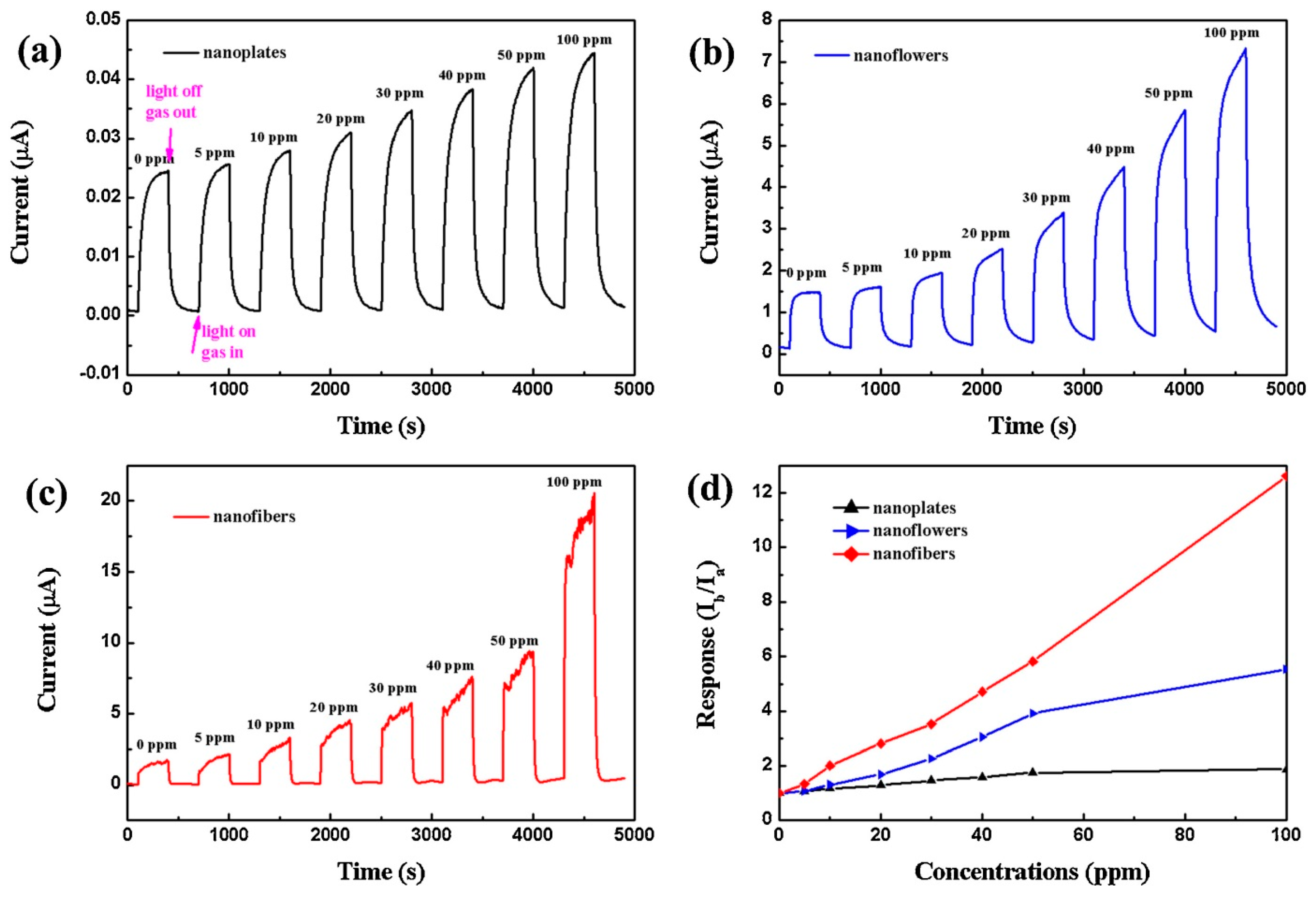
The wide array of achievable ZnO nanostructures has led to many groups with different backgrounds working on them yielding a massive range of reported applications. The listing of all of them lies beyond the scope and ability of this paper, however one of the most commercially successful are the low-voltage phosphors [179] and some of the most currently researched ones include gas sensors, photocatalytic degradation and biological-oriented applications. Gas sensors that use ZnO nanostructures make use of the above described mechanism and try to find the optimal morphologies or crystallite shapes for specific and fast responses [180,181,182] (see Figure 11). Likewise, in photocatalytic applications, ZnO nanostructures are researched for breakdown of waterborne pollutants, in particular persistent organic pollutants, that are not removable by traditional treatment processes [183]. It has to be noted that, as usual for catalysts, the ZnO can be immobilized or grafted onto porous media to achieve a larger effective surface available.
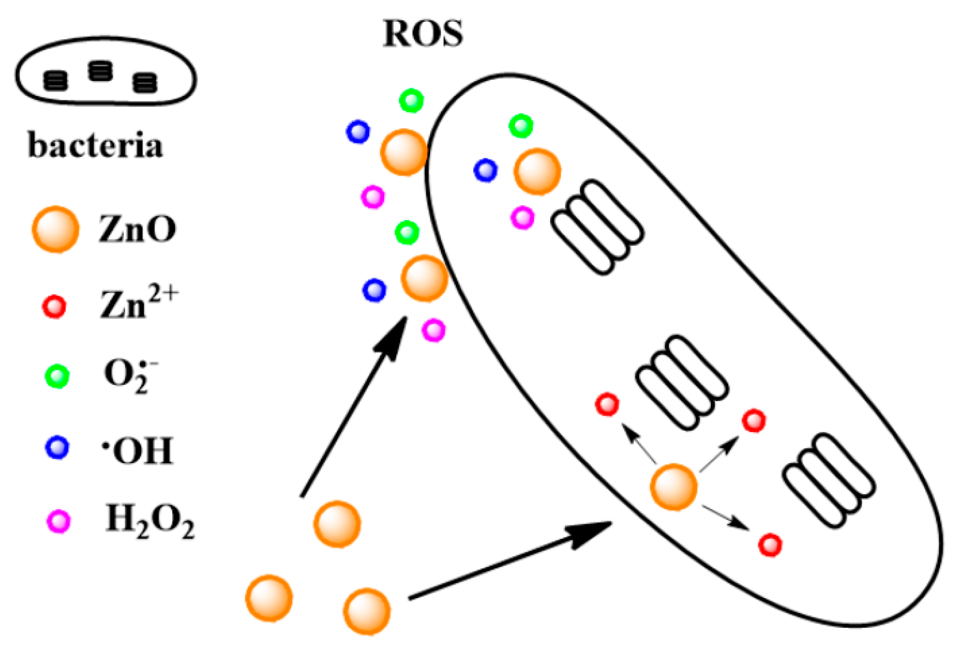
The biocompatibility of ZnO has generated interest in its applications in several areas related to medicine. Nanoparticles form the basis of ZnO implant coatings as described above, but also are investigated as biomarkers when doped with appropriate ions for selective luminescence [184]. Their cell-specific antibacterial activity (see Figure 12), very high for rapidly multiplying cells and much lower for quiescent ones has led to them been explored as anti-cancer agents [185]. Targeted drug delivery using ZnO nanoparticles is heavily explored [186] and, along with the anti-cancer activity, has been showing promising results in oncological in-vitro trials [187]. A new direction of ZnO nanoparticle study for biomedicine is its function as Zn source regulating insulin integrity in diabetic patients, promising results have been seen in vivo in animals with lowering of blood glucose and increase in insulin levels after administering of the ZnO nanoparticles [188]. The antimicrobial activity of ZnO is also explored in the nanoparticle functionalization of textiles and other materials [189].
A whole area of piezotronics was conceived using ZnO nanostructures in the form of springs, rods etc. on woven cloths. Here, the piezo-nanogenerators are used to harvest mechanical energy from the environment, that is often wasted or not harnessed, such as human steps in corridors, automobile traffic on the streets or even waves in the sea [190]. The same materials were shown to be promising for energy storage by example of wearable woven high capacitance supercapacitors [191] and the nanostructured ZnO was also reported as the basis of fully transparent stiff supercapacitors [192].
5. Unresolved Problems
Two of the biggest problems in the technology of ZnO related mostly to the physical and chemical worlds can be identified as: (1) the inability to obtain p-type conducting material that is highly conducting, reproducible, stable in time and with a well identifiable origin and (2) a wide range of synthesis conditions resulting in a larger-than-comprehensible zoo of various nanostructures with differing properties. The first problem is the reason why, widely regarded as the material to make GaN obsolete due to it’s much easier deposition and larger scale available, ZnO has since failed to deliver on that promise, despite many years of intensive research from the scientific community using a wide variety of state-of-the-art experimental growth and characterization techniques, supplemented by computation studies identifying appropriate dopants and complex doping strategies. The second one leads to a supersaturation of the literature with many similar reports on ZnO nanostructures, yielding the field very difficult to follow thoroughly, lowering the reproducibility and impact of the results, and also reducing the chances for new, valuable reports to be published. However, since the ZnO nanostructure synthesis community can be regarded as the developing one, while the p-type community as the diminishing one, the p-type doping problem will be discussed here in more detail due to its gravity.
P-Type Doping Issue in ZnO
The p-type conductivity in zinc oxide has long been a subject of extensive research and debate, however without significant consensus. Firstly, the potential acceptors are readily compensated by intrinsic impurity donors and intrinsic stable deep donor states. Secondly, the candidate acceptors have their ionization energies rather large in comparison to the ionization energies of shallow donors in ZnO. An additional difficulty lies in the observed formation of a surface electron accumulation layer in ZnO [193,194] which may render the conductivity measurements in the films if not performed with high rigor. Among the potential acceptors are column IA (Li, Na, K) and IB (Cu, Ag, Au) elements substituting Zn with ionization energies relative to the conduction band maximum calculated at 0.09 eV for LiZn, 0.17 eV for NaZn and 0.32 eV for KZn [195] and 0.25 eV–0.4 for AgZn [196,197,198], 0.35 for CuZn and 0.45 eV for AuZn [199]. Group IA elements have however small ionic radii and are more prone to go into interstitial positions not substitution and such interstitial dopants have first to be passivated before the ones occupying substitutional sites can be seen as acceptors. Group V elements substituting O have also been considered as potential acceptors with ionization energies calculated at 0.40 eV for NO, 0.93 eV for PO, and 1.15 eV for AsO with nitrogen being later reported to be deeper at 1.3 eV [200] using a modified theoretical approach. These levels may be regarded as too deep to provide efficient p-type conductivity in the material, however there have been reports on p-type ZnO films achieved experimentally using group IA [201], Ag [202,203] and group V acceptors [204,205,206,207,208]. It remains still to be shown that these results are stable and reproducible with p-type conductivity in ZnO being known to degrade over time [209,210]. Furthermore, no reliable results concerning ZnO p-n homojunctions were reported. If, however, there are stable p-type ZnO films achieved using the above described acceptors the effect may still be achieved by intentional and unintentional codoping or dopant complex formation. Donor-acceptor codoping may enhance acceptor solubility at the same time suppress the formation of compensating defects changing the growth conditions such as is the case of hydrogen doping during p-GaN:Mg growth [211]. It is relevant to notice, that this codoping may be intentional, e.g., using In [212], as well as unintentional due to the presence of impurities in the film such as H. Dual acceptor doping was reported to yield p-type ZnO thin films with As-N [213] and Li-N [214] dopants with acceptor activation energies in the latter at 95 meV. Generally dual acceptors complex may lead to formation of hybrid bonding states closer to the valence band maximum than the respective isolated acceptor states. Furthermore, although Ag-N pairs are expected to have deeper states than the isolated elements, Ag-N-H triangles may yield lower energy levels at 0.14 eV [215], showing that intrinsic impurities may have yet another way of influencing the conductivity of the films. Recent reports suggest that a new route towards obtaining shallower acceptor energies in ZnO is to use the traditional acceptors in ZnO alloyed by iso-valent elements such as Mg, Be, S, Se, or Te due to their possibility to push up the conduction band minimum or valence band maximum energies as well as the suppression of compensating intrinsic defects [216]. However, although there is much research effort along the new pathways, still no breakthrough is visible. A final comment here should be added here, that due to the problems with the electron accumulation layer, as well as grain boundary defect and dopant segregation, the Hall effect measurements performed using van der Pauw Hall configuration can lead to misleading effects. Therefore, it is highly desirable to perform experiments using high quality ZnO single crystal structures with the Hall effect measurements supplemented by Seebeck effect measurements, photoluminescence, and chemical characterization such as secondary ion mass spectrometry with a final verification in device operation such as a p-field effect transistor or a p-n/p-i-n diode.
6. Summary and Outlook
Zinc oxide has firmly marked its presence in the scientific community. It has not seen the spectacular success as it was expected due to the inherent difficulties in obtaining complementary conductivity types and the epitaxial n-type devices show limited performance in relation to the gallium nitride counterparts. It has however seen a significant surge in interest in the chemical community due to the wide variety of synthetic approaches it lends itself to and the broad array of achievable nanostructure morphologies that can be applied in many devices. The works on overcoming the p-type doping obstacle have died down in intensity but are still continued and should lead to a final success, however most probably the material will not be pure ZnO but some sort of an alloy or highly defected material due to the need to form complexes and co-dope. Opening up the way for p-type ZnO will lead to a revival of interest in the material as the common p-n devices will be developed, most notably for light emitters, which may finally realize the dream some have of phasing out GaN. The works on the 2DEG devices are limited due to much lower mobilities than in AlGaN/GaN structures and other ZnO film structures are mostly believed to be waiting for the stable p-type. ZnO single crystal substrates are emerging as price and size competitive substrates for GaN-based devices, however the growth processes for GaN are weary of oxide outdiffusion into the GaN layers, leading to uncontrolled compensation of the grown structures. ZnO single substrates are therefore not seen as the game changer for GaN devices in terms of lattice match and crystalline perfection, with most growth of the nitride occurring on the highly mismatched sapphire, silicon carbide and silicon. On the other hand, the nanostructured ZnO range is constantly developing and catching researcher interest. One of the most promising areas for these nanostructures is the sensor area where metal oxide devices are well established and ZnO can find relatively easy implemented applications. However, the nanostructured ZnO area seems to become saturated with reports where the different morphologies are often seen as ‘yet another’ report that does not contribute much to bridging the knowledge gap. It is probably the role of individual researchers to move from the synthesis to serious device development utilizing ZnO nanostructures to push for the market presence, otherwise the topic may be seen as stagnant. The need for a rigorous research approach is evident both for nanostructures where the experimental details have to be thoroughly controlled as for the films, where the various conductivity origins have to be thoroughly understood and presented. To summarize, ZnO is now in the stage where the initial hype has died down or is slowly saturating, and mostly comprehensive investigations are needed to push the material to deliver on its promising capabilities and fulfill its potential.
Author Contributions
M.A.B. is the sole author of this review.
Funding
This work received no external funding.
Acknowledgments
There are no acknowledgments for this work.
Conflicts of Interest
The author declares no conflict of interest.
References
- Frederickson, C.J.; Koh, J.-Y.; Bush, A.I. The neurobiology of zinc in health and disease. Nat. Rev. Neurosci. 2005, 6, 449–462. [Google Scholar] [CrossRef] [PubMed]
- Habashi, F. Zinc—The Metal from the East. Bull. Can. Inst. Min. Met. 2001, 94, 71–76. [Google Scholar]
- Biswas, A.K. Rasa–Ratna–Samuccaya and Mineral Processing State–of–Art in the 13th Century AD India. Indian J. Hist. Sci. 1987, 22, 22–46. [Google Scholar]
- Eastaugh, N.; Walsh, V.; Chaplin, T.; Siddall, R. Pigment. Compendium: A Dictionary and Optical Microscopy of Historic Pigments; Elsevier: Burlington, MA, USA, 2008. [Google Scholar]
- Moezzi, A.; McDonagh, A.M.; Cortie, M.B. Zinc oxide particles: Synthesis, properties and applications. Chem. Eng. J. 2012, 185–186, 1–22. [Google Scholar] [CrossRef]
- Brown, H.E. Zinc Oxide Rediscovered; The New Jersey Zinc Company: New York, NY, USA, 1957. [Google Scholar]
- Leong, E.S.P.; Yu, S.F.; Chong, M.K.; Tan, O.K.; Pita, K. Metal-oxide-SiO2 composite ZnO lasers. IEEE Photonics Technol. Lett. 2005, 17, 1815–1817. [Google Scholar] [CrossRef]
- Zhang, X.Q.; Suemune, I.; Kumano, H.; Yao, Z.G.; Huang, S.H. Room temperature ultraviolet lasing action in high-quality ZnO thin films. J. Lumin. 2007, 122, 828–830. [Google Scholar] [CrossRef]
- Chu, S.; Olmedo, M.; Yang, Z.; Kong, J.; Liu, J. Electrically pumped ultraviolet ZnO diode lasers on Si. Appl. Phys. Lett. 2008, 93, 181106. [Google Scholar] [CrossRef] [Green Version]
- Krishnamoorthy, S.; Iliadis, A.A. Properties of High Sensitivity ZnO Surface Acoustic Wave Sensors on SiO2/ (100) Si Substrates. Solid-State Electron. 2008, 52, 1710–1716. [Google Scholar] [CrossRef]
- Kumar, S.; Kim, G.H.; Sreenivas, K.; Tandon, R.P. ZnO based surface acoustic wave ultraviolet photo sensor. J. Electroceram. 2009, 22, 198–202. [Google Scholar] [CrossRef]
- Chivukula, V.; Ciplys, D.; Shur, M.; Dutta, P. ZnO nanoparticle surface acoustic wave UV sensor. Appl. Phys. Lett. 2010, 96, 233512. [Google Scholar] [CrossRef]
- Subramanian, V.; Bakhishev, T.; Redinger, D.; Volkman, S.K. Solution-Processed Zinc Oxide Transistors for Low-Cost Electronics Applications. J. Disp. Technol. 2009, 5, 525–530. [Google Scholar] [CrossRef]
- Dietl, T.; Ohno, H.; Matsukura, F.; Cibert, J.; Ferrand, D. Zener Model Description of Ferromagnetism in Zinc-Blende Magnetic Semiconductors. Science 2000, 287, 1019. [Google Scholar] [CrossRef] [PubMed]
- Liu, C.; Yun, F.; Morkoc, H. Ferromagnetism of ZnO and GaN: A Review. J. Mater. Sci. Mater. Electron. 2005, 16, 555–597. [Google Scholar] [CrossRef]
- Wang, H.T.; Kang, B.S.; Ren, F.; Tien, L.C.; Sadik, P.W.; Norton, D.P.; Pearton, S.J.; Lin, J. Hydrogen-selective sensing at room temperature with ZnO nanorods. Appl. Phys. Lett. 2005, 86, 243503. [Google Scholar] [CrossRef]
- Sadek, A.Z.; Choopun, S.; Wlodarski, W.; Ippolito, S.J.; Kalantar-zadeh, K. Characterization of ZnO Nanobelt-Based Gas Sensor for H2, NO2, and Hydrocarbon Sensing. IEEE Sens. J. 2007, 7, 919–924. [Google Scholar] [CrossRef]
- Phan, D.T.; Chung, G.S. Surface acoustic wave hydrogen sensors based on ZnO nanoparticles incorporated with a Pt catalyst. Sens. Actuators B Chem. 2012, 161, 341–348. [Google Scholar] [CrossRef]
- Han, J.; Fan, F.; Xu, C.; Lin, S.; Wei, M.; Duan, X.; Wang, Z.L. ZnO nanotube-based dye-sensitized solar cell and its application in self-powered devices. Nanotechnology 2010, 21, 405203. [Google Scholar] [CrossRef] [PubMed]
- Martinson, A.B.F.; Elam, J.W.; Hupp, J.T.; Pellin, M.J. ZnO Nanotube Based Dye-Sensitized Solar Cells. Nano Lett. 2007, 7, 2183–2187. [Google Scholar] [CrossRef] [PubMed]
- Jiang, Z.; Soltanian, S.; Gholamkhass, B.; Aljaafari, A.; Servati, P. Light-soaking free organic photovoltaic devices with sol–gel deposited ZnO and AZO electron transport layers. RSC Adv. 2018, 8, 36542–36548. [Google Scholar] [CrossRef]
- Morkoç, H.; Özgür, Ü. Zinc Oxide: Fundamentals, Materials and Device Technology, 1st ed.; WILEY-VCH Verlag GmbH & Co. KGaA: Weinheim, Germany, 2009. [Google Scholar]
- Thomas, D.G. The exciton spectrum of zinc oxide. J. Phys. Chem. Solids 1960, 15, 86–96. [Google Scholar] [CrossRef]
- Vigué, F.; Vennéguès, P.; Deparis, C.; Vézian, S.; Laügt, M.; Faurie, J.P. Growth modes and microstructures of ZnO layers deposited by plasma-assisted molecular-beam epitaxy on (0001) sapphire. J. Appl. Phys. 2001, 90, 5115. [Google Scholar] [CrossRef]
- Tsukazaki, A.; Ohtomo, A.; Kita, T.; Ohno, Y.; Ohno, H.; Kawasaki, M. Quantum Hall Effect in Polar Oxide Heterostructures. Science 2007, 315, 1388–1391. [Google Scholar] [CrossRef] [PubMed]
- Tampo, H.; Shibata, H.; Maejima, K.; Yamada, A.; Matsubara, K.; Fons, P.; Kashiwaya, S.; Niki, S.; Chiba, Y.; Wakamatsu, T.; et al. Polarization-induced two-dimensional electron gases in ZnMgO/ZnO heterostructures. Appl. Phys. Lett. 2008, 93, 202104. [Google Scholar] [CrossRef]
- Hwang, H.Y.; Iwasa, Y.; Kawasaki, M.; Keimer, B.; Nagaosa, N.; Tokura, Y. Emergent phenomena at oxide interfaces. Nat. Mater. 2012, 11, 103–113. [Google Scholar] [CrossRef] [PubMed]
- Hsu, H.C.; Wu, C.Y.; Cheng, H.M.; Hsieh, W.F. Band gap engineering and stimulated emission of ZnMgO nanowires. Appl. Phys. Lett. 2006, 89, 013101. [Google Scholar] [CrossRef]
- Ohtomo, A.; Tamura, K.; Kawasaki, M.; Makino, T.; Segawa, Y.; Tang, Z.K.; Wong, L.G.K.; Matsumoto, Y.; Koinuma, H. Room-temperature stimulated emission of excitons in ZnO/(Mg, Zn)O superlattices. Appl. Phys. Lett. 2000, 77, 2204. [Google Scholar] [CrossRef]
- Gruber, T.; Kirchner, C.; Kling, R.; Reuss, F.; Waag, A.; Bertram, F.; Forster, D.; Christen, J.; Schreck, M. Optical and structural analysis of ZnCdO layers grown by metalorganic vapor-phase epitaxy. Appl. Phys. Lett. 2003, 83, 3290. [Google Scholar] [CrossRef]
- Li, S.M.; Kwon, B.J.; Kwack, H.S.; Jin, L.H.; Cho, Y.H.; Park, Y.S.; Han, M.S.; Park, Y.S. Optical transition dynamics in ZnO/ZnMgO multiple quantum well structures with different well widths grown on ZnO substrates. J. Appl. Phys. 2010, 107, 033513. [Google Scholar] [CrossRef] [Green Version]
- Sadofev, S.; Blumstengel, S.; Cui, J.; Puls, J.; Rogaschewski, S.; Schafer, P.; Sadofyev, Y.G.; Henneberger, F. Growth of high-quality ZnMgO epilayers and ZnO/ZnMgO quantum well structures by radical-source molecular-beam epitaxy on sapphire. Appl. Phys. Lett. 2005, 87, 091903. [Google Scholar] [CrossRef]
- Available online: https://commons.wikimedia.org/wiki/File:Wurtzite_polyhedra.png (accessed on 17 August 2019).
- Look, D.C.; Hemsky, J.W.; Sizelove, J.R. Residual Native Shallow Donor in ZnO. Phys. Rev. Lett. 1999, 82, 2552. [Google Scholar] [CrossRef]
- Look, D.C. Recent advances in ZnO materials and devices. Mater. Sci. Eng. B 2001, 80, 383–387. [Google Scholar] [CrossRef]
- Lany, S.; Zunger, A. Anion vacancies as a source of persistent photoconductivity in II-VI and chalcopyrite semiconductors. Phys. Rev. B 2005, 72, 035215. [Google Scholar] [CrossRef] [Green Version]
- Lany, S.; Zunger, A. Dopability, Intrinsic Conductivity, and Nonstoichiometry of Transparent Conducting Oxides. Phys. Rev. Lett. 2007, 98, 045501. [Google Scholar] [CrossRef] [PubMed]
- Janotti, A.; Van de Walle, C.G. New insights into the role of native point defects in ZnO. J. Cryst. Growth 2006, 287, 58–65. [Google Scholar] [CrossRef]
- Janotti, A.; Van de Walle, C.G. Native point defects in ZnO. Phys. Rev. B 2007, 76, 165202. [Google Scholar] [CrossRef]
- Cuscó, R.; Alarcón-Lladó, E.; Ibáñez, J.; Artús, L.; Jiménez, J.; Wang, B.; Callahan, M.J. Temperature dependence of Raman scattering in ZnO. Phys. Rev. B 2007, 75, 165202. [Google Scholar] [CrossRef]
- Kohan, A.F.; Ceder, G.; Morgan, D.; Van de Walle, C.G. First-principles study of native point defects in ZnO. Phys. Rev. B 2000, 61, 15019. [Google Scholar] [CrossRef]
- Hu, J.; Gordon, R.G. Textured aluminum-doped zinc oxide thin films from atmospheric pressure chemical-vapor deposition. J. Appl. Phys. 1992, 71, 880. [Google Scholar] [CrossRef]
- Ko, H.J.; Chen, Y.F.; Hong, S.K.; Wenisch, H.; Yao, T.; Look, D.C. Ga-doped ZnO films grown on GaN templates by plasma-assisted molecular-beam epitaxy. Appl. Phys. Lett. 2000, 77, 3761. [Google Scholar] [CrossRef]
- Hu, J.; Gordon, R.G. Electrical and Optical Properties of Indium Doped Zinc Oxide Films Prepared by Atmospheric Pressure Chemical Vapor Deposition. Mater. Res. Soc. Symp. Proc. 1993, 283, 891. [Google Scholar] [CrossRef]
- Wenas, W.W.; Yamada, A.; Takahashi, K.; Yoshino, M.; Konagai, M. Electrical and optical properties of boron-doped ZnO thin films for solar cells grown by metalorganic chemical vapor deposition. J. Appl. Phys. 1991, 70, 7119. [Google Scholar] [CrossRef]
- Meyer, J.; Görrn, P.; Hamwi, S.; Johannes, H.H.; Riedl, T.; Kowalsky, W. Indium-free transparent organic light emitting diodes with Al doped ZnO electrodes grown by atomic layer and pulsed laser deposition. Appl. Phys. Lett. 2008, 93, 073308. [Google Scholar] [CrossRef]
- Zhang, S.B.; Wei, S.H.; Zunger, A. Intrinsic n-type versus p-type doping asymmetry and the defect physics of ZnO. Phys. Rev. B 2001, 63, 075205. [Google Scholar] [CrossRef]
- Hofmann, D.M.; Hofstaetter, A.; Leiter, F.; Zhou, H.; Henecker, F.; Meyer, B.K.; Orlinskii, S.B.; Schmidt, J.; Baranov, P.G. Hydrogen: A Relevant Shallow Donor in Zinc Oxide. Phys. Rev. Lett. 2002, 88, 045504. [Google Scholar] [CrossRef] [PubMed]
- Pankove, J.I.; Johnson, N.M. Hydrogen in Semiconductors, Semiconductors and Semimetals; Academic Press: Boston, MA, USA, 1991; Volume 34. [Google Scholar]
- Van de Walle, C.G. Hydrogen as a Cause of Doping in Zinc Oxide. Phys. Rev. Lett. 2000, 85, 1012–1015. [Google Scholar] [CrossRef] [PubMed] [Green Version]
- Nemanič, V.; Bogataj, T. Outgassing of thin wall stainless steel chamber. Vacuum 1998, 50, 431–437. [Google Scholar] [CrossRef]
- Ishikawa, Y.; Nemanič, V. An overview of methods to suppress hydrogen outgassing rate from austenitic stainless steel with reference to UHV and EXV. Vacuum 2003, 69, 501–512. [Google Scholar] [CrossRef]
- Čižek, J.; Valenta, J.; Hruška, P.; Melikhova, O.; Procházka, I.; Novotný, M.; Bulíř, J. Origin of green luminescence in hydrothermally grown ZnO single crystals. Appl. Phys. Lett. 2015, 106, 251902. [Google Scholar] [CrossRef]
- Doherty, R.P.; Sun, Y.; Sun, Y.; Warren, J.L.; Fox, N.A.; Cherns, D.; Ashfold, M.N.R. Growth of nanostructured ZnO thin films on sapphire. Appl. Phys. A 2007, 89, 49–55. [Google Scholar] [CrossRef]
- Vayssieres, L. Growth of Arrayed Nanorods and Nanowires of ZnO from Aqueous Solutions. Adv. Mater. 2003, 15, 464–466. [Google Scholar] [CrossRef]
- Kuo, C.L.; Kuo, T.J.; Huang, M.H. Hydrothermal synthesis of ZnO microspheres and hexagonal microrods with sheetlike and platelike nanostructures. J. Phys. Chem. B 2005, 109, 20115–20121. [Google Scholar] [CrossRef] [PubMed]
- Zhang, W.; Zhu, R.; Liu, X.; Liu, B.; Ramakrishna, S. Facile construction of nanofibrous ZnO photoelectrode for dye-sensitized solar cell applications. Appl. Phys. Lett. 2009, 95, 043304. [Google Scholar] [CrossRef] [Green Version]
- Chen, C.; Lu, Y.; He, H.; Wu, K.; Ye, Z. One-step synthesis of flower-like Au-ZnO microstructures at room temperature and their photocatalytic properties. Appl. Phys. A 2013, 110, 47–53. [Google Scholar] [CrossRef]
- Brayner, R.; Dahoumane, S.A.; Yéprémian, C.; Djediat, C.; Meyer, M.; Couté, A.; Fiévet, F. ZnO Nanoparticles: Synthesis, Characterization, and Ecotoxicological Studies. Langmuir 2010, 26, 6522–6528. [Google Scholar] [CrossRef] [PubMed]
- Matsuyama, K.; Mishima, K.; Kato, T.; Irie, K.; Mishima, K. Transparent polymeric hybrid film of ZnO nanoparticle quantum dots and PMMA with high luminescence and tunable emission color. J. Colloid Interface Sci. 2012, 367, 171–177. [Google Scholar] [CrossRef] [PubMed]
- Zhang, H.; Wu, R.; Chen, Z.; Liu, G.; Zhang, Z.; Jiao, Z. Self-assembly fabrication of 3D flower-like ZnO hierarchical nanostructures and their gas sensing properties. CrystEngComm 2012, 14, 1775–1782. [Google Scholar] [CrossRef]
- Ko, S.H.; Lee, D.; Kang, H.W.; Nam, K.H.; Yeo, J.Y.; Hong, S.J.; Grigoropoulos, C.P.; Sung, H.J. Nanoforest of Hydrothermally Grown Hierarchical ZnO Nanowires for a High Efficiency Dye-Sensitized Solar Cell. Nano Lett. 2011, 11, 666–671. [Google Scholar] [CrossRef] [PubMed]
- Wang, Z.L. Novel nanostructures of ZnO for nanoscale photonics, optoelectronics, piezoelectricity, and sensing. Appl. Phys. A 2007, 88, 7–15. [Google Scholar] [CrossRef]
- Li, L.; Pan, S.; Dou, X.; Zhu, Y.; Huang, X.; Yang, Y.; Li, G.; Zhang, L. Direct Electrodeposition of ZnO Nanotube Arrays in Anodic Alumina Membranes. J. Phys. Chem. C 2007, 111, 7288–7291. [Google Scholar] [CrossRef]
- Hu, F.; Chan, K.C.; Yue, T.M.; Surya, C. Dynamic Template Assisted Electrodeposition of Porous ZnO Thin Films Using a Triangular Potential Waveform. J. Phys. Chem. C 2010, 114, 5811–5816. [Google Scholar] [CrossRef]
- Yano, M.; Koike, K.; Ogata, K.; Nogami, T.; Tanabe, S.; Sasa, S. Zinc oxide-based biosensors. Phys. Status Solidi C 2012, 9, 1570–1573. [Google Scholar] [CrossRef]
- Borysiewicz, M.A.; Dynowska, E.; Kolkovsky, V.; Dyczewski, J.; Wielgus, M.; Kamińska, E.; Piotrowska, A. From porous to dense thin ZnO films through reactive DC sputter deposition onto Si (100) substrates. Phys. Status Solidi A 2012, 209, 2463–2469. [Google Scholar] [CrossRef]
- Ohshima, E.; Ogino, H.; Niikura, I.; Maeda, K.; Sato, M.; Ito, M.; Fukuda, T. Growth of the 2-in-size bulk ZnO single crystals by the hydrothermal method. J. Cryst. Growth 2004, 260, 166–170. [Google Scholar] [CrossRef]
- Hirose, M. Growth of Zinc Oxide Single Crystals by Vapor Phase Reaction. Jpn. J. Appl. Phys. 1971, 10, 401. [Google Scholar] [CrossRef]
- Wang, B.; Claflin, B.; Callahan, M.; Fang, Z.Q.; Look, D. Electrical and optical properties of ZnO bulk crystals with and without lithium grown by the hydrothermal technique. Proc. SPIE 2014, 8987, 89871D. [Google Scholar] [CrossRef]
- Johnson, M.A.L.; Fujita, S.; Rowland, W.H.; Hughes, W.C.; Cook, J.W.; Schetzina, J.F. MBE growth and properties of ZnO on sapphire and SiC substrates. J. Electron. Mater. 1996, 25, 855–862. [Google Scholar] [CrossRef]
- Cho, M.Y.; Kim, M.S.; Choi, H.Y.; Jeon, S.M.; Kim, G.S.; Kim, D.Y.; Yim, K.G.; Leem, J.-Y. Effects of Growth Interruption of ZnO Buffer Layers on the Structural and the Optical Properties of ZnO Thin Films Grown by Using PA-MBE. J. Korean Phys. Soc. 2010, 56, 1833–1837. [Google Scholar] [CrossRef]
- Pietrzyk, M.A.; Zielony, E.; Stachowicz, M.; Reszka, A.; Płaczek-Popko, E.; Wierzbicka, A.; Przezdziecka, E.; Droba, A.; Kozanecki, A. Electro-optical characterization of ZnO/ZnMgO structure grown on p-type Si (1 1 1) by PA-MBE method. J. Alloys Compd. 2014, 587, 724–728. [Google Scholar] [CrossRef]
- Kuznetsov, P.; Lusanov, V.; Yakushcheva, G.; Jitov, V.; Zakharov, L.; Kotelyanskii, I.; Kozlovsky, V. MOVPE growth and study of ZnO, ZnMgO epilayers and ZnO/ZnMgO MQW structures. IOP Conf. Ser. Mater. Sci. Eng. 2010, 8, 012040. [Google Scholar] [CrossRef]
- Kaidashev, E.M.; Lorenz, M.; von Wenckstern, H.; Rahm, A.; Semmelhack, H.-C.; Han, K.-H.; Benndorf, G.; Bundesmann, C.; Hochmuth, H.; Grundmann, M. High electron mobility of epitaxial ZnO thin films on c-plane sapphire grown by multistep pulsed-laser deposition. Appl. Phys. Lett. 2003, 82, 3901. [Google Scholar] [CrossRef]
- Nahnas, A.; Kim, H.K. Epitaxial growth of ZnO films on Si substrates using an epitaxial GaN buffer. Appl. Phys. Lett. 2001, 78, 1511. [Google Scholar] [CrossRef]
- Jin, B.J.; Im, S.; Lee, S.Y. Violet and UV luminescence emitted from ZnO thin films grown on sapphire by pulsed laser deposition. Thin Solid Films 2000, 366, 107–110. [Google Scholar] [CrossRef]
- Alfaro Cruz, M.R.; Ceballos-Sanchez, O.; Luévano-Hipólito, E.; Torres-Martínez, L.M. ZnO thin films deposited by RF magnetron sputtering: Effects of the annealing and atmosphere conditions on the photocatalytic hydrogen production. Int. J. Hydrogen Energy 2018, 43, 10301–10310. [Google Scholar] [CrossRef]
- Borysiewicz, M.A.; Pasternak, I.; Dynowska, E.; Jakieła, R.; Kolkovki, V.; Dużyńska, A.; Kamińska, E.; Piotrowska, A. ZnO Thin Films Deposited on Sapphire by High Vacuum High Temperature Sputtering. Acta Phys. Pol. A 2011, 119, 686–688. [Google Scholar] [CrossRef]
- Särkijärvi, S.; Sintonen, S.; Tuomisto, F.; Bosund, M.; Suihkonen, S.; Lipsanen, H. Effect of growth temperature on the epitaxial growth of ZnO on GaN by ALD. J. Cryst. Growth 2014, 398, 18–22. [Google Scholar] [CrossRef]
- Guziewicz, E.; Kowalik, I.A.; Godlewski, M.; Kopalko, K.; Osinniy, V.; Wójcik, A.; Yatsunenko, S.; Łusakowska, E.; Paszkowicz, W.; Guziewicz, M. Extremely low temperature growth of ZnO by atomic layer deposition. J. Appl. Phys. 2008, 103, 033515. [Google Scholar] [CrossRef]
- Minami, T.; Nanoto, H.; Takata, S. Highly Conductive and Transparent Aluminum Doped Zinc Oxide Thin Films Prepared by RF Magnetron Sputtering. Jpn. J. Appl. Phys. 1984, 23, L280. [Google Scholar] [CrossRef]
- Lim, S.J.; Kwon, S.-J.; Kim, H.; Park, J.-S. High performance thin film transistor with low temperature atomic layer deposition nitrogen-doped ZnO. Appl. Phys. Lett. 2008, 91, 183517. [Google Scholar] [CrossRef]
- Kamalasanan, M.N.; Chandra, S. Sol-gel synthesis of ZnO thin films. Thin Solid Films 1996, 288, 112–115. [Google Scholar] [CrossRef]
- Bao, D.; Gu, H.; Kuang, A. Sol–gel-derived c-axis oriented ZnO thin films. Thin Solid Films 1998, 312, 37–39. [Google Scholar] [CrossRef]
- Studenikin, S.A.; Golego, N.; Cocivera, M. Fabrication of green and orange photoluminescent, undoped ZnO films using spray pyrolysis. J. Appl. Phys. 1998, 84, 2287–2294. [Google Scholar] [CrossRef]
- Wu, Y.; Girgis, E.; Ström, V.; Voit, W.; Belova, L.; Rao, K.V. Ultraviolet light sensitive In-doped ZnO thin film field effect transistor printed by inkjet technique. Phys. Status Solidi A 2010, 208, 206–209. [Google Scholar] [CrossRef]
- Manzano, C.V.; Alegre, D.; Caballero-Calero, O.; Alén, B.; Martín-González, M.S. Synthesis and luminescence properties of electrodeposited ZnO films. J. Appl. Phys. 2011, 110, 043538. [Google Scholar] [CrossRef] [Green Version]
- Azeez, O.A.; Sabry, R.S.; Hassan, M.A.M.; Madlul, S.F. Synthesis and characteristics of screen printed ZnO thick films nanostructures grown using different methods. J. Mater. Sci. Mater. Electron. 2015, 26, 4051–4061. [Google Scholar] [CrossRef] [Green Version]
- Ge, C.; Xie, C.; Cai, S. Preparation and gas-sensing properties of Ce-doped ZnO thin-film sensors by dip-coating. Mater. Sci. Eng. B 2007, 137, 53–58. [Google Scholar] [CrossRef]
- Saleh, S.M. ZnO nanospheres based simple hydrothermal route for photocatalytic degradation of azo dye. Spectrochim. Acta Part A Mol. Biomol. Spectrosc. 2019, 211, 141–147. [Google Scholar] [CrossRef] [PubMed]
- Sahu, K.; Kuriakose, S.; Singh, J.; Satpati, B.; Mohapatra, S. Facile synthesis of ZnO nanoplates and nanoparticle aggregates for highly efficient photocatalytic degradation of organic dyes. J. Phys. Chem. Solids 2018, 121, 186–195. [Google Scholar] [CrossRef]
- Pimentel, A.; Henriques Ferreira, S.; Nunes, D.; Calmeiro, T.; Martins, R.; Fortunato, E. Microwave Synthesized ZnO Nanorod Arrays for UV Sensors: A Seed Layer Annealing Temperature Study. Materials 2016, 9, 299. [Google Scholar] [CrossRef]
- Samadipakchin, P.; Mortaheb, H.R.; Zolfaghari, A. ZnO nanotubes: Preparation and photocatalytic performance evaluation. J. Photochem. Photobiol. A Chem. 2017, 337, 91–99. [Google Scholar] [CrossRef]
- Li, Y.B.; Bando, Y.; Golberg, D. ZnO nanoneedles with tip surface perturbations: Excellent field emitters. Appl. Phys. Lett. 2004, 84, 3603. [Google Scholar] [CrossRef]
- All Abbas, J.M.; Narin, P.; Kutlu, E.; Lisesivdin, S.B.; Ozbay, E. Electronic properties of zigzag ZnO nanoribbons with hydrogen and magnesium passivations. Phys. B Condens. Matter 2019, 556, 12–16. [Google Scholar] [CrossRef]
- Shi, Y.; Bao, S.; Shi, R.; Huang, C.; Amini, A.; Wu, Z.; Zhang, L.; Wang, N.; Cheng, C. Y-shaped ZnO Nanobelts Driven from Twinned Dislocations. Sci. Rep. 2016, 6, 22494. [Google Scholar] [CrossRef] [PubMed]
- Zhang, X.; Zhou, Y.Z.; Wu, D.Y.; Liu, X.H.; Zhang, R.; Liu, H.; Dong, C.K.; Yang, J.; Kulinich, S.A.; Du, X.W. ZnO nanosheets with atomically thin ZnS overlayers for photocatalytic water splitting. J. Mater. Chem. A 2018, 6, 9057–9063. [Google Scholar] [CrossRef]
- Mahendra, R.; Arianti, M.; Sawitri, D.; Risanti, D.D. Synthesis of Various ZnO Nanotree Morphologies through PEG-Assisted Co-Precipitation Method. Adv. Mater. Res. 2015, 1112, 66–70. [Google Scholar] [CrossRef]
- Zhuo, R.F.; Feng, H.T.; Chen, J.T.; Yan, D.; Feng, J.J.; Li, H.J.; Geng, B.S.; Cheng, S.; Xu, X.Y.; Yan, P.X. Multistep Synthesis, Growth Mechanism, Optical, and Microwave Absorption Properties of ZnO Dendritic Nanostructures. J. Phys. Chem. C 2008, 112, 11767–11775. [Google Scholar] [CrossRef]
- Ren, D.; Li, J.; Bao, Y.; Wu, Z.; He, S.; Wang, A.; Guo, F.; Chen, Y. Low-temperature synthesis of flower-like ZnO microstructures supported on TiO2 thin films as efficient antifungal coatings for bamboo protection under dark conditions. Colloids Surf. A Physicochem. Eng. Asp. 2018, 555, 381–388. [Google Scholar] [CrossRef]
- Leung, Y.H.; Tam, K.H.; Djurišić, A.B.; Xie, M.H.; Chan, W.K.; Lu, D.; Ge, W.K. ZnO nanoshells: Synthesis, structure, and optical properties. J. Cryst. Growth 2005, 283, 134–140. [Google Scholar] [CrossRef]
- Borysiewicz, M.A.; Wzorek, M.; Wojciechowski, T.; Wojtowicz, T.; Kamińska, E.; Piotrowska, A. Photoluminescence of nanocoral ZnO films. J. Lumin. 2014, 147, 367–371. [Google Scholar] [CrossRef]
- Tong, Y.; Liu, Y.; Dong, L.; Zhao, D.; Zhang, J.; Lu, Y.; Shen, D.; Fan, X. Growth of ZnO nanostructures with different morphologies by using hydrothermal technique. J. Phys. Chem. B 2006, 110, 20263–20267. [Google Scholar] [CrossRef]
- Li, P.; Wei, Z.; Wu, T.; Peng, Q.; Li, Y. Au−ZnO Hybrid Nanopyramids and Their Photocatalytic Properties. J. Am. Chem. Soc. 2011, 133, 5660–5663. [Google Scholar] [CrossRef]
- Agrawal, J.; Dixit, T.; Palani, I.A.; Rao, M.S.R.; Singh, V. Fabrication of high responsivity deep UV photo-detector based on Na doped ZnO nanocolumns. J. Phys. D Appl. Phys. 2018, 51, 185106. [Google Scholar] [CrossRef]
- Saleema, N.; Farzaneh, M. Thermal effect on superhydrophobic performance of stearic acid modified ZnO nanotowers. Appl. Surf. Sci. 2008, 254, 2690–2695. [Google Scholar] [CrossRef]
- Fan, D.; Zhang, R.; Li, Y. Synthesis and optical properties of phosphorus-doped ZnO nanocombs. Solid State Commun. 2010, 150, 1911–1914. [Google Scholar] [CrossRef]
- Wang, Z.L. Nanostructures of zinc oxide. Mater. Today 2004, 7, 26–33. [Google Scholar] [CrossRef]
- Gao, P.X.; Wang, Z.L. High-Yield Synthesis of Single-Crystal Nanosprings of ZnO. Small 2005, 1, 945–949. [Google Scholar] [CrossRef] [PubMed]
- Zhang, Y.; Ram, M.K.; Stefanakos, E.K.; Goswami, Y.D. Synthesis, Characterization, and Applications of ZnO Nanowires. J. Nanomater. 2012, 2012, 624520. [Google Scholar] [CrossRef]
- Li, W.; Wu, X.; Han, N.; Chen, J.; Qian, X.; Deng, Y.; Tang, W.; Chen, Y. MOF-derived hierarchical hollow ZnO nanocages with enhanced low-concentration VOCs gas-sensing performance. Sens. Actuators B Chem. 2016, 225, 158–166. [Google Scholar] [CrossRef]
- Warule, S.S.; Chaudhari, N.S.; Ambekar, J.D.; Kale, B.B.; More, M.A. Hierarchical Nanostructured ZnO with Nanorods Engendered to Nanopencils and Pin-Cushion Cactus with Its Field Emission Study. ACS Appl. Mater. Interfaces 2011, 3, 3454–3462. [Google Scholar] [CrossRef] [PubMed]
- Witkowski, B.S.; Wachnicki, Ł.; Gieraltowska, S.; Sybilski, P.; Kopalko, K.; Stachowicz, M.; Godlewski, M. UV detector based on zinc oxide nanorods obtained by the hydrothermal method. Phys. Status Solidi C 2014, 11, 1447–1451. [Google Scholar] [CrossRef]
- Rai, P.; Kwak, W.K.; Yu, Y.T. Solvothermal Synthesis of ZnO Nanostructures and Their Morphology-Dependent Gas-Sensing Properties. ACS Appl. Mater. Interfaces 2013, 5, 3026–3032. [Google Scholar] [CrossRef]
- Wasly, H.S.; El-Sadek, M.S.A.; Henini, M. Influence of reaction time and synthesis temperature on the physical properties of ZnO nanoparticles synthesized by the hydrothermal method. Appl. Phys. A 2018, 124, 76. [Google Scholar] [CrossRef] [Green Version]
- Widiyastuti, W.; Machmudah, S.; Nurtono, T.; Winardi, S.; Balgis, R.; Ogi, T.; Okuyama, K. Morphology and optical properties of zinc oxide nanoparticles synthesized by solvothermal method. Chem. Eng. Trans. 2017, 56, 955–960. [Google Scholar] [CrossRef]
- Martin, O.; González, V.; Tirado, M.; Comedi, D. Effects of methanol on morphology and photoluminescence in solvothermal grown ZnO powders and ZnO on Si. Mater. Lett. 2019, 251, 41–44. [Google Scholar] [CrossRef]
- Ghorbani, H.R.; Mehr, F.P.; Pazoki, H.; Rahmani, B.M. Synthesis of ZnO Nanoparticles by Precipitation Method. Orient J. Chem 2015, 31, 1219–1221. [Google Scholar] [CrossRef]
- Wojnarowicz, J.; Chudoba, T.; Gierlotka, S.; Łojkowski, W. Effect of Microwave Radiation Power on the Size of Aggregates of ZnO NPs Prepared Using Microwave Solvothermal Synthesis. Nanomaterials 2018, 8, 343. [Google Scholar] [CrossRef] [PubMed]
- Chen, S.; Kumar, R.V.; Gedanken, A.; Zaban, A. Sonochemical synthesis of crystalline nanoporous zinc oxide spheres and their application in dye-sensitized solar cells. Isr. J. Chem. 2001, 41, 51–54. [Google Scholar] [CrossRef]
- Applerot, G.; Perkas, N.; Amirian, G.; Girshevitz, O.; Gedanken, A. Coating of glass with ZnO via ultrasonic irradiation and a study of its antibacterial properties. Appl. Surf. Sci. 2009, 256 (Suppl. 15), S3–S8. [Google Scholar] [CrossRef]
- Di Mauro, A.; Zimbone, M.; Fragalà, M.E.; Impellizzeri, G. Synthesis of ZnO nanofibers by the electrospinning process. Mater. Sci. Semicond. Process. 2016, 42, 98–101. [Google Scholar] [CrossRef]
- Keong, C.C.; Vivek, Y.S.; Salamatinia, B.; Horri, B.A. Green Synthesis of ZnO Nanoparticles by an Alginate Mediated Ion-Exchange Process and a case study for Photocatalysis of Methylene Blue Dye. J. Phys. Conf. Ser. 2017, 829, 012014. [Google Scholar] [CrossRef] [Green Version]
- Ao, W.; Li, J.; Yang, H.; Zeng, X.; Ma, X. Mechanochemical synthesis of zinc oxide nanocrystalline. Powder Technol. 2006, 168, 148–151. [Google Scholar] [CrossRef]
- Zacour Marinho, J.; da Costa Romeiro, F.; Lemos, S.C.S.; Motta, F.V.; Riccardi, C.; Siu Li, M.; Longo, E.; Lima, R.C. Urea-Based Synthesis of Zinc Oxide Nanostructures at Low Temperature. J. Nanomater. 2012, 2012, 427172. [Google Scholar] [CrossRef]
- Zhu, Y.; Apostoluk, A.; Gautier, P.; Valette, A.; Omar, L.; Cornier, T.; Bluet, J.M.; Masenelli-Varlot, K.; Daniele, S.; Masenelli, B. Intense visible emission from ZnO/PAAX (X = H or Na) nanocomposite synthesized via a simple and scalable sol-gel method. Sci. Rep. 2016, 6, 23557. [Google Scholar] [CrossRef] [PubMed]
- Wong, E.M.; Hoertz, P.G.; Liang, C.J.; Shi, B.M.; Meyer, G.J.; Searson, P.C. Influence of Organic Capping Ligands on the Growth Kinetics of ZnO Nanoparticles. Langmuir 2001, 17, 8362–8367. [Google Scholar] [CrossRef]
- Xiong, H.M.; Liu, D.P.; Xia, Y.Y.; Chen, J.S. Polyether-grafted ZnO Nanoparticles with Tunable and Stable Photoluminescence at Room Temperature. Chem. Mater. 2005, 17, 3062–3064. [Google Scholar] [CrossRef]
- Shaikh, T.; Sharma, A.; Kaur, H. Ultrasonication Assisted Synthesis of 3 Substituted Indoles in Water Using Polymer Grafted ZnO Nanoparticles as Eco-Friendly Catalyst. ChemistrySelect 2019, 4, 245–249. [Google Scholar] [CrossRef]
- Hong, R.Y.; Qian, J.Z.; Cao, J.X. Synthesis and Characterization of PMMA grafted ZnO nanoparticles. Powder Technol. 2006, 163, 160–168. [Google Scholar] [CrossRef]
- Abdolrezapour, F.; Moradi, M. High optical quality long ultrafine ZnO nanowires by low-temperature oxidation of sputtered nanostructured Zn templates. Int. J. Mod. Phys. B 2018, 32, 1850297. [Google Scholar] [CrossRef]
- Huang, M.H.; Wu, Y.; Feick, H.; Tran, N.; Weber, E.; Yang, P. Catalytic Growth of Zinc Oxide Nanowires by Vapor Transport. Adv. Mater. 2001, 13, 113–116. [Google Scholar] [CrossRef]
- Yao, B.D.; Chan, Y.F.; Wang, N. Formation of ZnO nanostructures by a simple way of thermal evaporation. Appl. Phys. Lett. 2002, 81, 757–759. [Google Scholar] [CrossRef]
- Bae, S.Y.; Na, C.W.; Kang, J.H.; Park, J. Comparative Structure and Optical Properties of Ga-, In-, and Sn-Doped ZnO Nanowires Synthesized via Thermal Evaporation. J. Phys. Chem. B 2005, 109, 2526–2531. [Google Scholar] [CrossRef]
- Borysiewicz, M.A.; Gryglas-Borysiewicz, M.; Masłyk, M.; Wojciechowski, T.; Wzorek, M.; Kaczmarski, J.; Wojtowicz, T.; Kamińska, E. Room temperature sputter deposited catalyst-free nanowires with wurtzite/zinc blende ZnO superstructure and their application in electromechanical nanogenerators on polymer and paper substrates. Nanotechnology 2017, 28, 085204. [Google Scholar] [CrossRef] [PubMed]
- Al-Salman, H.S.; Abdullah, M.J. Preparation of ZnO nanostructures by RF-magnetron sputtering on thermally oxidized porous silicon substrate for VOC sensing application. Measurement 2015, 59, 248–257. [Google Scholar] [CrossRef]
- Sundara Venkatesh, P.; Kulandaivel, J. Investigations on the morphological evolution of zinc oxide nanostructures and their optical properties. Cryst. Eng. Comm. 2014, 16, 7426. [Google Scholar] [CrossRef]
- Arroyo-Hernández, M.; Alvaro, R.; Serrano, S.; Luis Costa-Krämer, J. Catalytic growth of ZnO nanostructures by r.f. magnetron sputtering. Nanoscale Res. Lett. 2011, 6, 437. [Google Scholar] [CrossRef]
- Isakov, I.; Panfilova, M.; Sourribes, M.J.L.; Warburton, P.A. Growth of ZnO and ZnMgO nanowires by Au-catalysed molecular-beam epitaxy. Phys. Status Solidi C 2013, 10, 1308. [Google Scholar] [CrossRef]
- Kennedy, O.W.; Coke, M.L.; White, E.R.; Shaffer, M.S.P.; Warburton, P.A. MBE growth and morphology control of ZnO nanobelts with polar axis perpendicular to growth direction. Mater. Lett. 2018, 212, 51–53. [Google Scholar] [CrossRef]
- Sallet, V.; Agouram, S.; Falyouni, F.; Marzouki, A.; Haneche, N.; Sartel, C.; Lusson, A.; Enouz-Vedrenne, S.; Munoz-Sanjose, V.; Galtier, P. Structural characterization of one-dimensional ZnO-based nanostructures grown by MOCVD. Phys. Status Solidi B 2010, 247, 1683. [Google Scholar] [CrossRef]
- Lee, W.; Jeong, M.C.; Myoung, J.M. Catalyst-free growth of ZnO nanowires by metal-organic chemical vapour deposition (MOCVD) and thermal evaporation. Acta Mater. 2004, 52, 3949. [Google Scholar] [CrossRef]
- Szczepanik, A.; Wachnicki, Ł.; Godlewski, M.; Guziewicz, E.; Kopalko, K.; Janik, E.; Łusakowska, E.; Czerwiński, A.; Płuska, M.; Yatsunenko, S.A. ZnO nanostructures by atomic layer deposition method. J. Phys. Conf. Ser. 2009, 146, 012017. [Google Scholar] [CrossRef]
- Fan, G.; Jiao, W.; Yang, L.; Wu, X.; Chen, M.; Gao, R.; Li, Y.; Xie, B.; Liu, J.; Han, M.; et al. Effects of hydriding and ageing of Pd nanoparticles to contact between nanoparticles and quartz and contacts among nanoparticles investigated by the pump-probe technique. Chem. Phys. Lett. 2016, 661, 191. [Google Scholar] [CrossRef]
- Zhao, S.; Yao, C.; Lu, Q.; Song, F.; Wan, J.; Wang, G. Cluster-assembled cobalt doped ZnO nanostructured film prepared by low energy cluster beam deposition. Trans. Nonferrous Met. Soc. China 2009, 19, 1450. [Google Scholar] [CrossRef]
- Tsukazaki, A.; Akasaka, S.; Nakahara, K.; Ohno, Y.; Ohno, H.; Maryenko, D.; Ohtomo, A.; Kawasaki, M. Observation of the fractional quantum Hall effect in an oxide. Nat. Mater. 2010, 9, 889–893. [Google Scholar] [CrossRef] [PubMed]
- Sasa, S.; Maitani, T.; Furuya, Y.; Amano, T.; Koike, K.; Yano, M.; Inoue, M. Microwave performance of ZnO/ZnMgO heterostructure field effect transistors. Phys. Status Solidi A 2011, 208, 449–452. [Google Scholar] [CrossRef]
- Wojtasiak, W.; Góralczyk, M.; Gryglewski, D.; Zając, M.; Kucharski, R.; Prystawko, P.; Piotrowska, A.; Ekielski, M.; Kamińska, E.; Taube, A.; et al. AlGaN/GaN High Electron Mobility Transistors on Semi-Insulating Ammono-GaN Substrates with Regrown Ohmic Contacts. Micromachines 2018, 9, 546. [Google Scholar] [CrossRef] [PubMed]
- Shubina, T.V.; Toropov, A.A.; Lublinskaya, O.G.; Kop’ev, P.S.; Ivanov, S.V.; El-Shaer, A.; Al-Suleiman, M.; Bakin, A.; Waag, A.; Voinilovich, A.; et al. Recombination dynamics and lasing in ZnO/ZnMgO single quantum well structures. Appl. Phys. Lett. 2007, 91, 201104. [Google Scholar] [CrossRef]
- Chou, H.C.; Mazady, A.; Zeller, J.; Manzur, T.; Anwar, M. Room-Temperature Quantum Cascade Laser: ZnO/Zn1−xMgxO Versus GaN/AlxGa1−xN. J. Electron. Mater. 2013, 42, 882–888. [Google Scholar] [CrossRef]
- Yan, X.; Li, W.; Aberle, A.G.; Venkataraj, S. Textured AZO for thin-film Si solar cells: Towards understanding the effect of AZO film thickness on the surface texturing properties. Procedia Eng. 2016, 139, 134–139. [Google Scholar] [CrossRef]
- Dong, H.; Pang, S.; Zhang, Y.; Chen, D.; Zhu, W.; Xi, H.; Chang, J.; Zhang, J.; Zhang, C.; Hao, Y. Improving Electron Extraction Ability and Device Stability of Perovskite Solar Cells Using a Compatible PCBM/AZO Electron Transporting Bilayer. Nanomaterials 2018, 8, 720. [Google Scholar] [CrossRef]
- Kan, Z.; Wang, Z.; Firdaus, Y.; Babics, M.; Alshareef, H.N.; Beaujuge, P.M. Atomic-layer-deposited AZO outperforms ITO in high-efficiency polymer solar cells. J. Mater. Chem. A 2018, 6, 10176–10183. [Google Scholar] [CrossRef] [Green Version]
- Liu, H.; Liu, Y.F.; Xiong, P.P.; Chen, P.; Li, H.Y.; Hou, J.W.; Kang, B.N.; Duan, Y. Aluminum-Doped Zinc Oxide Transparent Electrode Prepared by Atomic Layer Deposition for Organic Light Emitting Devices. IEEE Trans. Nanotechnol. 2017, 16, 634–638. [Google Scholar] [CrossRef]
- Hsu, C.H.; Chen, S.Y.; Chen, W.C.; Chang, C.H.; Chen, C.Y.; Tsai, J.H.; Liu, W.C. Study of a GaN-Based LED with an Al/AZO Composite Transparent Conductive Layer. IEEE Trans. Electron. Devices 2017, 64, 3678–3682. [Google Scholar] [CrossRef]
- Al Eghfeli, M.; Abdul Hadi, S.; El Atab, N.; Nayfeh, A. Demonstration of aluminum doped ZnO as anti-reflection coating. In Proceedings of the 2016 IEEE 43rd Photovoltaic Specialists Conference (PVSC), Portland, OR, USA, 5–10 June 2016; pp. 2765–2769. [Google Scholar] [CrossRef]
- Chowdhury, A.R.; Rao, V.P.; Ghosh, B.; Banerjee, S. Antireflection coating on solar cell using ZnO nanostructure. AIP Conf. Proc. 2012, 1447, 777. [Google Scholar] [CrossRef]
- Grundmann, M.; Frenzel, H.; Lajn, A.; Lorenz, M.; Schein, F.; von Wenckstern, H. Transparent semiconducting oxides: Materials and devices. Phys. Status Solidi A 2010, 207, 1437–1449. [Google Scholar] [CrossRef]
- Faber, H.; Das, S.; Lin, Y.H.; Pliatsikas, N.; Zhao, K.; Kehagias, T.; Dimitrakopulos, G.; Amassian, A.; Patsalas, P.A.; Anthopoulos, T.D. Heterojunction oxide thin-film transistors with unprecedented electron mobility grown from solution. Sci. Adv. 2017, 3, e1602640. [Google Scholar] [CrossRef] [PubMed]
- Qin, W.; Li, T.; Li, Y.; Qiu, J.; Ma, X.; Chen, X.; Hu, X.; Zhang, W. A high power ZnO thin film piezoelectric generator. Appl. Surf. Sci. 2016, 364, 670–675. [Google Scholar] [CrossRef]
- Lai, S.L.; Zakaria, M.R.; Hashim, U.; Foo, K.L.; Haarindra Prasad, R. Fabrication of SAW device by using ZnO thin film as a sensing area. In Proceedings of the 2014 IEEE International Conference on Semiconductor Electronics (ICSE2014), Kuala Lumpur, Malaysia, 27–29 August 2014; pp. 380–383. [Google Scholar] [CrossRef]
- Du, X.; Fu, Y.; Tan, S.C.; Luo, J.; Flewitt, A.; Maeng, S.; Kim, S.H.; Choi, Y.; Lee, D.S.; Park, R.M.; et al. ZnO film based surface acoustic wave micro-pump. J. Phys. Conf. Ser. 2007, 76, 012047. [Google Scholar] [CrossRef]
- Santos, Y.P.; Valença, E.; Machado, R.; Macêdo, M.A. A novel structure ZnO-Fe-ZnO thin film memristor. Mater. Sci. Semicond. Process. 2018, 86, 43–48. [Google Scholar] [CrossRef]
- Kim, K.K.; Kim, H.S.; Hwang, D.K.; Lim, J.H.; Park, S.J. Realization of p-type ZnO thin films via phosphorus doping and thermal activation of the dopant. Appl. Phys. Lett. 2003, 83, 63. [Google Scholar] [CrossRef]
- Snigurenko, D.; Kopalko, K.; Krajewski, T.A.; Jakiela, R.; Guziewicz, E. Nitrogen doped p-type ZnO films and p-n homojunction. Semicond. Sci. Technol. 2015, 30, 015001. [Google Scholar] [CrossRef]
- Bu, I.Y.Y. Sol-gel production of p-type ZnO thin film by using sodium doping. Superlattices Microstruct. 2016, 96, 59–66. [Google Scholar] [CrossRef]
- Li, G.; Wang, H.; Wang, Q.; Zhao, Y.; Wang, Z.; Du, J.; Ma, Y. Structure and properties of Co-doped ZnO films prepared by thermal oxidization under a high magnetic field. Nanoscale Res. Lett. 2015, 10, 112. [Google Scholar] [CrossRef] [PubMed]
- Hadimani, P.L.; Ghosh, S.S.; Sil, A. Preparation of Fe doped ZnO thin films and their structural, magnetic, electrical characterization. Superlattices Microstruct. 2018, 120, 199–208. [Google Scholar] [CrossRef]
- Agarwal, D.C.; Singh, U.B.; Gupta, S.; Singhal, R.; Kulriya, P.K.; Singh, F.; Tripathi, A.; Singh, J.; Joshi, U.S.; Avasthi, D.K. Enhanced room temperature ferromagnetism and green photoluminescence in Cu doped ZnO thin film synthesised by neutral beam sputtering. Sci. Rep. 2019, 9, 6675. [Google Scholar] [CrossRef] [PubMed]
- Levinson, L.; Philipp, H.R. Zinc oxide varistors—A review. Am. Ceram. Soc. Bull. 1986, 65, 639–646. [Google Scholar]
- Wallenhorst, L.; Gurău, L.; Gellerich, A.; Militz, H.; Ohms, G.; Viöla, W. UV-blocking properties of Zn/ZnO coatings on wood deposited by cold plasma spraying at atmospheric pressure. Appl. Surf. Sci. 2018, 434, 1183–1192. [Google Scholar] [CrossRef]
- Carvalho, J.T.; Dubceac, V.; Grey, P.; Cunha, I.; Fortunato, E.; Martins, R.; Clausner, A.; Zschech, E.; Pereira, L. Fully Printed Zinc Oxide Electrolyte-Gated Transistors on Paper. Nanomaterials 2019, 9, 169. [Google Scholar] [CrossRef]
- Grey, P.; Gaspar, D.; Cunha, I.; Barras, R.; Carvalho, J.T.; Ribas, J.R.; Fortunato, E.; Martins, R.; Pereira, L. Handwritten Oxide Electronics on Paper. Adv. Mater. Technol. 2017, 2, 1700009. [Google Scholar] [CrossRef]
- Kim, J.J.; Kim, K.S.; Jung, G.Y. Fabrication of flexible dye-sensitised solar cells with photoanodes composed of periodically aligned single crystalline vertical ZnO NRs by utilising a direct metal transfer method. J. Mater. Chem 2011, 21, 7730–7735. [Google Scholar] [CrossRef]
- Wagh, M.S.; Jain, G.H.; Patil, D.R.; Patil, S.A.; Patil, L.A. Modified zinc oxide thick film resistors as NH3 gas sensor. Sens. Actuators B Chem. 2006, 115, 128–133. [Google Scholar] [CrossRef]
- Neelakantan, N.K.; Weisensee, P.B.; Overcash, J.W.; Torrealba, E.J.; King, W.P.; Suslick, K.S. Spray-on omniphobic ZnO coatings. RSC Adv. 2015, 5, 69243–69250. [Google Scholar] [CrossRef]
- Memarzadeh, K.; Sharili, A.S.; Huang, J.; Rawlinson, S.C.F.; Allaker, R.P. Nanoparticulate zinc oxide as a coating material for orthopedic and dental implants. J. Biomed. Mater. Res. Part A 2015, 103A, 981–989. [Google Scholar] [CrossRef] [PubMed]
- Vogel, E.M.; Nelson, T.J. Novel synthesis and characterization of ZnO-based phosphors. Displays 1986, 7, 78–80. [Google Scholar] [CrossRef]
- Gong, H.; Hu, J.Q.; Wang, J.H.; Ong, C.H.; Zhu, F.R. Nano-crystalline Cu-doped ZnO thin film gas sensor for CO. Sens. Actuators B Chem. 2006, 115, 247–251. [Google Scholar] [CrossRef]
- Kumar, R.; Al-Dossary, O.; Kumar, G.; Umar, A. Zinc Oxide Nanostructures for NO2 Gas Sensor Applications: A Review. Nano-Micro Lett. 2015, 7, 97–120. [Google Scholar] [CrossRef]
- Agarwal, S.; Rai, P.; Navarrete Gatell, E.; Llobet, E.; Güelle, F.; Kumar, M.; Awasthi, K. Gas sensing properties of ZnO nanostructures (flowers/rods) synthesized by hydrothermal method. Sens. Actuators B Chem. 2019, 292, 24–31. [Google Scholar] [CrossRef]
- Ong, C.B.; Ng, L.Y.; Mohammad, A.W. A review of ZnO nanoparticles as solar photocatalysts: Synthesis, mechanisms and applications. Renew. Sustain. Energy Rev. 2018, 81, 536–551. [Google Scholar] [CrossRef]
- Wolska, E.; Kaszewski, J.; Kiełbik, P.; Grzyb, J.; Godlewski, M.M.; Godlewski, M. Rare earth activated ZnO nanoparticles as biomarkers. Opt. Mater. 2014, 36, 1655–1659. [Google Scholar] [CrossRef]
- Premanathan, M.; Karthikeyan, K.; Jeyasubramanian, K.; Manivannan, G. Selective toxicity of ZnO nanoparticles toward Gram-positive bacteria and cancer cells by apoptosis through lipid peroxidation. Nanomed. Nanotechnol. Biol. Med. 2011, 7, 184–192. [Google Scholar] [CrossRef] [PubMed]
- Wang, J.; Lee, J.S.; Kim, D.; Zhu, L. Exploration of zinc oxide nanoparticles as a multitarget and multifunctional anticancer nanomedicine. ACS Appl. Mater. Interfaces 2017, 9, 39971–39984. [Google Scholar] [CrossRef]
- Wang, J.; Gao, S.; Wang, S.; Xu, Z.; Wei, L. Zinc oxide nanoparticles induce toxicity in CAL 27 oral cancer cell lines by activating PINK1/Parkin-mediated mitophagy. Int. J. Nanomed. 2018, 13, 3441–3450. [Google Scholar] [CrossRef]
- Jiang, J.; Pi, J.; Cai, J. The Advancing of Zinc Oxide Nanoparticles for Biomedical Applications. Bioinorg. Chem. Appl. 2018, 2018, 1062562. [Google Scholar] [CrossRef] [PubMed]
- Shateri-Khalilabad, M.; Yazdanshenas, M.E. Bifunctionalization of cotton textiles by ZnO nanostructures: Antimicrobial activity and ultraviolet protection. Text. Res. J. 2013, 83, 993–1004. [Google Scholar] [CrossRef]
- Wang, Z.L.; Wu, W.; Falconi, C. Piezotronics and piezo-phototronics with third-generation semiconductors. MRS Bull. 2018, 43, 922–927. [Google Scholar] [CrossRef] [Green Version]
- Bae, J.; Song, M.K.; Park, Y.J.; Kim, J.M.; Liu, M.; Wang, Z.L. Fiber Supercapacitors Made of Nanowire-Fiber Hybrid Structures for Wearable/Flexible Energy Storage. Angew. Chem. Int. Ed. 2011, 50, 1683–1687. [Google Scholar] [CrossRef] [PubMed]
- Borysiewicz, M.A.; Ekielski, M.; Ogorzałek, Z.; Wzorek, M.; Kaczmarski, J.; Wojciechowski, T. Highly transparent supercapacitors based on ZnO/MnO2 nanostructures. Nanoscale 2017, 9, 7577–7587. [Google Scholar] [CrossRef] [PubMed]
- Schmidt, O.; Kiesel, P.; Van de Walle, C.G.; Johnson, N.M.; Nause, J.; Döhler, G.H. Effects of an Electrically Conducting Layer at the Zinc Oxide Surface. Jpn. J. Appl. Phys. 2005, 144, 7271. [Google Scholar] [CrossRef]
- Look, D.C. Quantitative analysis of surface donors in ZnO. Surf. Sci. 2007, 601, 5315–5319. [Google Scholar] [CrossRef]
- Park, G.H.; Zhang, S.B.; Wei, S.H. Origin of p-type doping difficulty in ZnO: The impurity perspective. Phys. Rev. B 2002, 66, 073202. [Google Scholar] [CrossRef]
- Volnianska, O.; Boguslawski, P.; Kaczkowski, J.; Jakubas, P.; Jezierski, A.; Kaminska, E. Theory of doping properties of Ag acceptors in ZnO. Phys. Rev. B 2009, 80, 245212. [Google Scholar] [CrossRef]
- Chai, J.; Mendelsberg, R.J.; Reeves, R.J.; Kennedy, J.; von Wenckstern, H.; Schmidt, M.; Grundmann, M.; Doyle, K.; Myers, T.H.; Durbin, S.M. Identification of a Deep Acceptor Level in ZnO Due to Silver Doping. J. Electron. Mater. 2010, 39, 577–583. [Google Scholar] [CrossRef]
- Yan, Y.; Al-Jassim, M.M.; Wei, S.H. Doping of ZnO by group-IB elements. Appl. Phys. Lett. 2006, 89, 181912. [Google Scholar] [CrossRef]
- Kaminska, E.; Pasternak, I.; Boguslawski, P.; Jezierski, A.; Dynowska, E.; Jakiela, R.; Przezdziecka, E.; Piotrowska, A.; Kossut, J. Group IB acceptors in ZnO: Experiment and theory. AIP Conf. Proc. 2009, 1199, 120–121. [Google Scholar] [CrossRef]
- Lyons, L.; Janotti, A.; Van de Walle, C.G. Why nitrogen cannot lead to p-type conductivity in ZnO. Appl. Phys. Lett. 2009, 95, 252105. [Google Scholar] [CrossRef]
- Meyer, B.K.; Stehr, J.; Hofstaetter, A.; Volbers, N.; Zeuner, A.; Sann, J. On the role of group I elements in ZnO. Appl. Phys. A 2007, 88, 119–123. [Google Scholar] [CrossRef]
- Deng, R.; Yao, B.; Li, Y.F.; Yang, T.; Li, B.H.; Zhang, Z.Z.; Shan, C.X.; Zhang, J.Y.; Shen, D.Z. Influence of oxygen/argon ratio on structural, electrical and optical properties of Ag-doped ZnO thin films. J. Cryst. Growth 2010, 312, 1813–1816. [Google Scholar] [CrossRef]
- Gruzintsev, A.N.; Volkov, V.T.; Khodos, I.I. Photoelectric properties of ZnO films doped with Cu and Ag acceptor impurities. Semiconductors 2003, 37, 259–262. [Google Scholar] [CrossRef]
- Yao, B.; Guan, L.X.; Xing, G.Z.; Zhang, Z.Z.; Li, B.H.; Wei, Z.P.; Wang, X.H.; Cong, C.X.; Xie, Y.P.; Lu, Y.M.; et al. P-type conductivity and stability of nitrogen-doped zinc oxide prepared by magnetron sputtering. J. Lumin. 2007, 122–123, 191–194. [Google Scholar] [CrossRef]
- Lim, J.H.; Kang, C.K.; Kim, K.K.; Park, I.K.; Hwang, D.K.; Park, S.J. UV Electroluminescence Emission from ZnO Light-Emitting Diodes Grown by High-Temperature Radiofrequency Sputtering. Adv. Mater. 2006, 18, 2720–2724. [Google Scholar] [CrossRef]
- Wang, X.H.; Yao, B.; Zhang, Z.Z.; Li, B.H.; Wei, Z.P.; Shen, D.Z.; Lu, Y.M.; Fan, X.W. The mechanism of formation and properties of Li-doped p-type ZnO grown by a two-step heat treatment. Semicond. Sci. Technol. 2006, 21, 494. [Google Scholar] [CrossRef]
- Qin, J.M.; Yao, B.; Yan, Y.; Zhang, J.Y.; Jia, X.P.; Zhang, Z.Z.; Li, B.H.; Shan, C.X.; Shen, D.Z. Formation of stable and reproducible low resistivity and high carrier concentration p-type ZnO doped at high pressure with Sb. Appl. Phys. Lett. 2009, 95, 022101. [Google Scholar] [CrossRef]
- Lin, S.S.; Lu, J.G.; Ye, Z.Z.; He, H.P.; Gu, X.Q.; Chen, L.X.; Huang, J.Y.; Zhao, B.H. P-type behavior in Na-doped ZnO films and ZnO homojunction light-emitting diodes. Solid State Commun. 2008, 148, 25–28. [Google Scholar] [CrossRef]
- Look, D.C.; Reynolds, D.C.; Litton, C.W.; Jones, R.L.; Eason, D.B.; Cantwell, G. Characterization of homoepitaxial p-type ZnO grown by molecular beam epitaxy. Appl. Phys. Lett. 2002, 81, 1830. [Google Scholar] [CrossRef]
- Wang, L.G.; Zunger, A. Cluster-Doping Approach for Wide-Gap Semiconductors: The Case of p-Type ZnO. Phys. Rev. Lett. 2003, 90, 256401. [Google Scholar] [CrossRef] [PubMed]
- Neugebauer, J.; Van de Walle, C.G. Role of hydrogen in doping of GaN. Appl. Phys. Lett. 1996, 68, 1829. [Google Scholar] [CrossRef]
- Chen, L.L.; Lu, J.G.; Ye, Z.Z.; Lin, Y.M.; Zhao, B.H.; Ye, Y.M.; Li, J.S.; Zhu, L.P. P-type behavior in In–N codoped ZnO thin films. Appl. Phys. Lett. 2005, 87, 252106. [Google Scholar] [CrossRef]
- Krtschil, A.; Dadgar, A.; Oleynik, N.; Bläsing, J.; Diez, A.; Krost, A. Local p-type conductivity in zinc oxide dual-doped with nitrogen and arsenic. Appl. Phys. Lett. 2005, 87, 262105. [Google Scholar] [CrossRef]
- Lu, J.G.; Zhang, Y.Z.; Ye, Z.Z.; Zhu, L.P.; Wang, L.; Zhao, B.H.; Liang, Q.L. Low-resistivity, stable p-type ZnO thin films realized using a Li–N dual-acceptor doping method. Appl. Phys. Lett. 2006, 88, 222114. [Google Scholar] [CrossRef]
- Volnianska, O.; Bogusławski, P.; Kaminska, E. Ag and N acceptors in ZnO: An ab initio study of acceptor pairing, doping efficiency, and the role of hydrogen. Phys. Rev. B 2012, 85, 165212. [Google Scholar] [CrossRef]
- Tang, K.; Gu, S.L.; Ye, J.D.; Zhu, S.M.; Zhang, R.; Zheng, Y.D. Recent progress of the native defects and p-type doping of zinc oxide. Chin. Phys. B 2017, 26, 047702. [Google Scholar] [CrossRef]
Figure 1.
ZnO wurtzite cell, Zn in yellow, O in grey, the tetrahedral coordination is shown for both types of atoms. Source: [33], public domain.
Figure 1.
ZnO wurtzite cell, Zn in yellow, O in grey, the tetrahedral coordination is shown for both types of atoms. Source: [33], public domain.

Figure 2.
The variation (a) BPR—beam-equivalent-pressure ratio of Mg to Zn beams during MBE growth, (b) c-lattice constant, and (c) room temperature band gap versus Mg content. In 700 nm thick ZnMgO MBE-grown epilayers. Inset: optical transmission spectra for x = 0.10 (right), 0.40 (left). Reprinted from Sadofev, S., Blumstengel, S., Cui, J., Puls, J., Rogaschewski, S., Schäfer, P., Sadofyev, Yu. G., and Henneberger, F., Growth of high-quality ZnMgO epilayers and ZnO/ZnMgO quantum well structures by radical-source molecular-beam epitaxy on sapphire, Appl. Phys. Lett., 2005, 87, 091903; doi:10.1063/1.2034113, with the permission of AIP Publishing.

Figure 3.
Two-inch size ZnO crystals produced during one hydrothermal growth run. Reprinted from Ehrentraut, D., Sato, H., Kagamitani, Y., Sato, H., Yoshikawa, A., Fukuda, T., Solvothermal growth of ZnO, Progress in Crystal Growth and Characterization of Materials 2006, 52, 280–335; doi:10.1016/j.pcrysgrow.2006.09.002, Copyright (2006), with permission from Elsevier.

Figure 4.
Schematic diagram of three basic growth modes: (a) layer-by-layer growth mode; (b) island growth mode; and (c) Stranski–Krastanov mode.
Figure 4.
Schematic diagram of three basic growth modes: (a) layer-by-layer growth mode; (b) island growth mode; and (c) Stranski–Krastanov mode.

Figure 5.
Schematic representation of dependence of coating structure on substrate temperature and argon pressure for sputter deposition, that is representative of most achievable thin film morphologies by other methods, but not necessarily in the same parameter space. The number-letter codes describe the different morphologies in detail in the source communication. Reprinted from Thornton A.J., Influence of apparatus geometry and deposition conditions on the structure and topography of thick sputtered coatings, J. Vacuum Sci. Technol. 1974, 11, 666; doi:10.1116/1.1312732 with the permission of AIP Publishing.

Figure 6.
SEM top view and cross section images of different screen printed ZnO film thickness (a) 15, (b) 7, (c) 3 and (d) 1 μm. The porous morphology is evident. Reprinted from Sun, H., Kimura, T., Chiba, T., Mori, S., Khosla, A., and Yoshida, T., High Voltage Flexible ZnO Solar Cells Employing Bulky Organic Dye and [Co(bpy)3]2+/3+ Redox Electrolyte, J. Electrochem. Soc. 2018, 165, B3194-B3200; doi:10.1149/2.0251808jes under the CC BY 4.0 license.

Figure 7.
A collection of nanostructures of ZnO synthesized under controlled conditions by thermal evaporation of solid powders. Reprinted from Wang, Z.L., Nanostructures of zinc oxide, Mater. Today 2004, 7, 26–33; doi:10.1016/S1369-7021(04)00286-X, Copyright (2004), with permission from Elsevier.
Figure 7.
A collection of nanostructures of ZnO synthesized under controlled conditions by thermal evaporation of solid powders. Reprinted from Wang, Z.L., Nanostructures of zinc oxide, Mater. Today 2004, 7, 26–33; doi:10.1016/S1369-7021(04)00286-X, Copyright (2004), with permission from Elsevier.

Figure 8.
(a) Photoluminescence (1) and photoluminescence emission (PLE) (2) spectra measured in a 3nm ZnO/ZnMgO SQW separate confinement double heterostructure. The room temperature PLE spectrum is monitored from the “green” PL peak (2.393eV) for the sake of better resolution. (b) RT spectra of stimulated emission measured at the excitation power density (from bottom to top): 436, 674, 872, and 1079 kW/cm2. The inset presents the PL intensity dependence on the excitation power. Reprinted from [140], with the permission of AIP Publishing.

Figure 9.
(a) UV AlGaN/GaN LED structure used in the experiment; (b) irradiated power as a function of diode current for the LED with Ni/Au, ZnO:Al and ZnMgO:Al contact electrodes; photographs and plan-view schematics of the LEDs with a Ni/Au electrode (c) and a ZnMgO:Al transparent electrode (d) showing increased output for the bandgap-engineered AZO electrode. Reprinted from Borysiewicz, M. A., Wzorek, M., Gołaszewska, K., Kruszka, R., Pągowska, K. D., Kamińska, E., Nanocrystalline sputter-deposited ZnMgO:Al transparent p-type electrode in GaN-based 385 nm UV LED for significant emission enhancement, Materials Science and Engineering: B 2015, 200, 93–98; doi:10.1016/j.mseb.2015.06.013, Copyright (2015) with permission from Elsevier.

Figure 10.
(a) Schematic representation of the fabrication steps for the fully printed ZnO electrolyte-gated transistors (EGTs). (b,c) and (d,e) Topographical views of the screen-printed layers using two different ZnO inks. Reprinted from [173] under the CC BY 4.0 license.
Figure 10.
(a) Schematic representation of the fabrication steps for the fully printed ZnO electrolyte-gated transistors (EGTs). (b,c) and (d,e) Topographical views of the screen-printed layers using two different ZnO inks. Reprinted from [173] under the CC BY 4.0 license.

Figure 11.
The current response cycles of ZnO nanoplates (a), nanoflowers (b) and nanofibers (c) to different concentrations of formaldehyde and the gas-sensing responses (d) with a bias voltage of 10 V under 365 nm light irradiation at room temperature. Reprinted from Cui, J., Shi, L., Xie, T., Wang, D., Lin, Y., UV-light illumination room temperature HCHO gas-sensing mechanism of ZnO with different nanostructures, Sensors and Actuators B: Chemical, 2016, 227, 220–226; doi:10.1016/j.snb.2015.12.010, Copyright (2016) with permission from Elsevier.

Figure 12.
Schematic illustration of antibacterial activity of ZnO NPs. In the outer cell membrane of the bacteria, an excess of reactive oxygen species (ROS) is expected and a release of Zn2+ ions, which in high concentration are cytotoxic. Reprinted from Zhang, Z.Y., and Xiong, H.M., Photoluminescent ZnO Nanoparticles and Their Biological Applications, Materials 2015, 8(6), 3101–3127; doi:10.3390/ma8063101, under the CC BY 4.0 license.

© 2019 by the author. Licensee MDPI, Basel, Switzerland. This article is an open access article distributed under the terms and conditions of the Creative Commons Attribution (CC BY) license (http://creativecommons.org/licenses/by/4.0/).
Share and Cite
MDPI and ACS Style
Borysiewicz, M.A. ZnO as a Functional Material, a Review. Crystals 2019, 9, 505. https://doi.org/10.3390/cryst9100505
AMA Style
Borysiewicz MA. ZnO as a Functional Material, a Review. Crystals. 2019; 9(10):505. https://doi.org/10.3390/cryst9100505
Chicago/Turabian StyleBorysiewicz, Michał A. 2019. "ZnO as a Functional Material, a Review" Crystals 9, no. 10: 505. https://doi.org/10.3390/cryst9100505
Note that from the first issue of 2016, this journal uses article numbers instead of page numbers. See further details here.