Review

Anti-Solvent Crystallization Strategies for Highly Efficient Perovskite Solar Cells

by
Maria Konstantakou
1,
Dorothea Perganti
1,2,3,
Polycarpos Falaras
2 and
Thomas Stergiopoulos
1,*
1
Laboratory of Physical Chemistry, Department of Chemistry, Aristotle University of Thessaloniki, Thessaloniki 54124, Greece
2
Institute of Nanoscience and Nanotechnology, National Centre for Scientific Research Demokritos, Athens 15310, Greece
3
School of Chemical Engineering, National Technical University of Athens, Athens 15780, Greece
*
Author to whom correspondence should be addressed.
Crystals 2017, 7(10), 291; https://doi.org/10.3390/cryst7100291
Submission received: 3 September 2017 / Revised: 25 September 2017 / Accepted: 26 September 2017 / Published: 28 September 2017

Abstract

:
Solution-processed organic-inorganic halide perovskites are currently established as the hottest area of interest in the world of photovoltaics, ensuring low manufacturing cost and high conversion efficiencies. Even though various fabrication/deposition approaches and device architectures have been tested, researchers quickly realized that the key for the excellent solar cell operation was the quality of the crystallization of the perovskite film, employed to assure efficient photogeneration of carriers, charge separation and transport of the separated carriers at the contacts. One of the most typical methods in chemistry to crystallize a material is anti-solvent precipitation. Indeed, this classical precipitation method worked really well for the growth of single crystals of perovskite. Fortunately, the method was also effective for the preparation of perovskite films by adopting an anti-solvent dripping technique during spin-coating the perovskite precursor solution on the substrate. With this, polycrystalline perovskite films with pure and stable crystal phases accompanied with excellent surface coverage were prepared, leading to highly reproducible efficiencies close to 22%. In this review, we discuss recent results on highly efficient solar cells, obtained by the anti-solvent dripping method, always in the presence of Lewis base adducts of lead(II) iodide. We present all the anti-solvents that can be used and what is the impact of them on device efficiencies. Finally, we analyze the critical challenges that currently limit the efficacy/reproducibility of this crystallization method and propose prospects for future directions.

1. Introduction

Halide perovskite solar cells were introduced for the first time in 2009 [1] and it then took three years for devices to attain power conversion efficiencies (PCEs) higher than ~10% under standard 1 sun AM1.5G illumination [2,3,4]. Within less than a year, the efficiencies went up to 15% using a so-called two-step solution [5] or a vapor deposition [6] processes. However, the most influential publications in the field (in our opinion) came with the introduction of anti-solvent crystallization in 2014; a poor solvent is poured onto the precursor perovskite film during spin coating, causing the salts to precipitate out of solution into a smooth, compact film [7,8]. Notably, in one of the publications, anti-solvent crystallization was combined with evidences that the perovskite forms through an intermediate that includes methylammonium iodide (MAI), PbI2 and dimethylsulfoxide (DMSO). The presence of this intermediate (or adduct) was indispensable in order to deliver hysteresis-free efficiencies over 16% [8]. Then a scientific “full moon” hit the field, motivating independent laboratories to adopt intermediate/anti-solvent crystallization in order to further enhance the efficiencies. Luckily, PCEs went up to close to 22% [9] within three years of experiments, utilizing various device architectures, passivation strategies and mixed perovskites. These PCEs are equivalent to others attained from emerging thin-film technologies such as CdTE and CIGS solar cells [10]. Notably, this success story found also application in other optoelectronic devices such as photodetectors and LEDs [11].
There are already literature reviews on perovskite film formation where the adduct/anti-solvent crystallization process is included [12,13,14,15,16,17]. However, at least according to our knowledge, there is no work describing in detail results adopting solely this method. More specifically here, we attempt to describe the method in comparison with typical anti-solvent precipitation that grows perovskite single crystals. We discuss the role of the stable MAI·PbI2·DMSO adduct and how we can achieve this intermediate phase through control of the precursor solution stoichiometry. We demonstrate all the recent results based on record PCEs attained from various types of devices based on typical MAPbI3 or mixed FA1−xMAxPbI3−yBry perovskites (where FA stands for formamidinium cation). Emphasis is given on novel approaches based on MAI or PbI2-excessive perovskite precursor solutions as well as on the addition of inorganic cations (Cs+ and Rb+) in order to fabricate optimal films. We also review very recent results where dripping an anti-solvent is accompanied by the deposition of an active compound at the very top surface of the perovskite. Finally, we provide all the range of anti-solvents used thus far, suggesting the five more promising systems.
Reading this review, one will always meet the terms “stabilized” (or steady-state) and/or “reverse scan” efficiency. We would like to clarify here that we refer to the scan-rate dependent hysteresis in the J-V curves of the perovskite solar cells. When current is measured from reverse-to-forward bias sweep direction (called reverse scan by us), an overestimation of the photovoltaic performance is taking place. In turn, if voltage is swept oppositely, one finds lower performances. As a consequence, recommendations are suggested so as to show photovoltaic behavior without masking the detrimental hysteresis effect. This is often realized by the “stabilized efficiency” experiment; thus, with the term “stabilized” efficiency, we refer to the determined value of the efficiency after holding the tested device at a constant voltage around the maximum power-point and track the power-output until it reaches a constant value [18].

2. Anti-solvent Precipitation Method to Grow Perovskite Single Crystals

2.1. Solution Processed Growth of Perovskite Single Crystals: The Conventional Way

The typical method to grow perovskite single crystals of high quality out of solution employs a large excess of HI/H2O as the reaction solvent. Precipitation in a solution occurs rapidly when the concentration of a compound exceeds its solubility, e.g., from a supersaturated solution. Supersaturation can be easily achieved for instance by cooling. As a general rule, the more heat is added to a system, the more soluble a substance becomes (this is not the case for various perovskites-in-solvent systems [19]). Therefore, at high temperatures, more solute can be dissolved than at room temperature. If this solution was to be suddenly cooled at a rate faster than the rate of precipitation, the solution will become supersaturated until the solute precipitates to the temperature-determined saturation point. With this, pure stoichiometric compounds are isolated with a very low carrier concentration (being nearly intrinsic) [20].

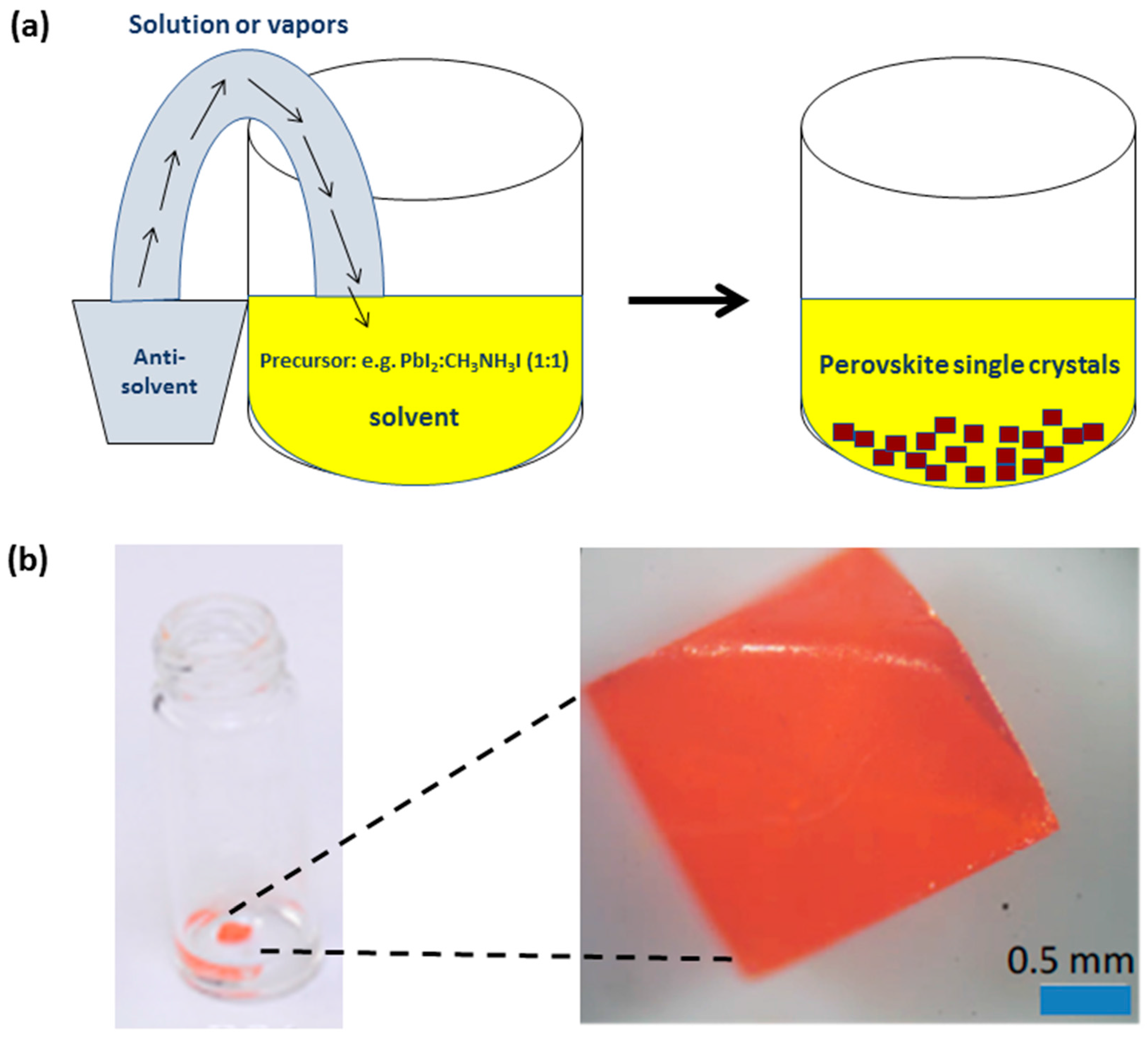
2.2. Anti-Solvent Precipitation: A Short Description

In another approach, supersaturation can be simply realized by exposing a solution of the product to another solvent (or multiple ones) in which the product is sparingly soluble (thus called anti-solvent). Again, precipitation will occur since the solubility of the desired product will be drastically reduced (Figure 1a). The efficacy of the approach (or otherwise stated, the quality of the crystals) depends on several parameters such as the nature of the anti-solvent being used, the volume ratio between solvent and anti-solvent, the exact time of the diffusion of the anti-solvent, the diffusion rate etc.

2.3. MAPbBr3 Single Crystals Grown Via Anti-Solvent (IPA) Precipitation

The first work on the anti-solvent precipitation method came out on June 2014. Tidhar et al. have grown MAPbBr3 single crystals by slowly adding isopropanol (IPA) vapors in the precursors dissolved in pure dimethylformamide (DMF); cubic perovskite crystals of large size were formed within 10–12 h (Figure 1b). The authors could not apply the same method to grow crystals for the MAPbI3 perovskite [21].

2.4. MAPbBr3 and MAPbI3 Single Crystals Grown Via Anti-Solvent (DCM) Precipitation

In a seminal work, submitted on January 2015 in Science, Shi et al. took the approach in a step forward. They replaced IPA by dichloromethane (DCM), which is a much poorer solvent of the perovskite (IPA can dissolve one of the constituents of the precursor, i.e., MAI or MABr). Vapors of DCM were allowed to diffuse into the precursor solutions that employed highly polar but non-highly coordinating solvents. Slow diffusion was chosen in order to develop adequate surface area to primarily achieve growth (vs. nucleation). With this, the ionic building blocks of the perovskite were co-precipitated from solution stoichiometrically, producing high-quality, millimeter-sized single crystals. Interestingly, these crystals exhibited exceptionally low trap densities (109–1010 cm−3) and impressively long diffusion lengths exceeding 10 µm [22]. We should state here that this was the first work ever to grow single crystals of MAPbI3 following anti-solvent crystallization; to achieve that, the authors have used an excess of MAI (PbI2:MAI = 1:3) in gamma-butyrolactone, gBL (instead of a stoichiometric 1:1 molar ratio of PbBr2:MABr in DMF, being employed for the crystals of MAPbBr3).

3. Anti-Solvent Dripping Technique to Prepare Polycrystalline Perovskite Films

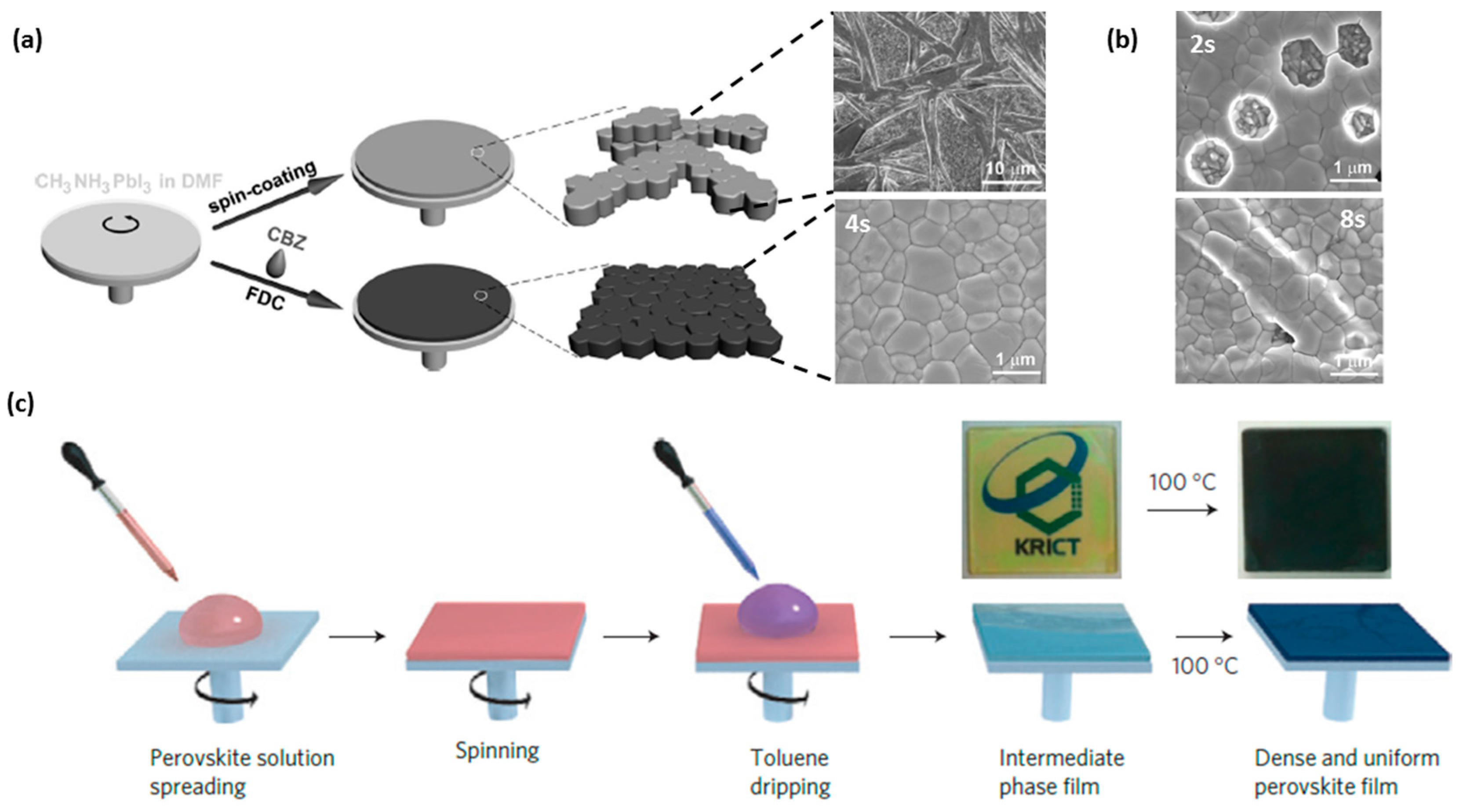
3.1. Anti-Solvent Dripping: An Introduction

Normally, to replicate the anti-solvent precipitation procedure, one should prepare yellow films of MAI:PbI2 (1:1) out of solution in an aprotic solvent (recall that this is a yellow solution) via spin-coating, and then inject the anti-solvent to immediately form a dark brown/red perovskite film; this film has to be purified (separation from mother liquor is not a prerequisite here as in the case of anti-solvent precipitation) by removing any additional phases, impurities (usually by copious washing with ethanol [20]) and the anti-solvent itself. There are inherently two main issues here: first crystallization of the film during spin-coating is quite fast, producing a perovskite film with bad morphology and very low surface coverage; if one injects the anti-solvent on top after the end of spinning (or if one simply immerses the “bad” film in a bath of anti-solvent), nothing will change. This implies that the anti-solvent needs to be dripped at a certain point (and quite quickly) during spinning. The second issue is that after forming a perovskite film (at the end of spin-coating), a proper procedure has to be adopted in order to get rid of all the stuff that are unnecessary (anything that is not MAPbI3). This suggests that perovskite films should be washed with an appropriate solvent and dried adequately so that impurities evaporate out of the film.

3.2. Anti-Solvent (CB) Dripping Using Precursor Solution Dissolved Solely in DMF

Simultaneously with the first work on anti-solvent precipitation for the growth of single crystals, two papers on anti-solvent crystallized perovskite films appeared in literature. First, Xiao et al. fabricated, inside a N2-filled glovebox, compact films with full surface coverage by employing a fast deposition-crystallization (FDC) procedure when dripping an anti-solvent during the first seconds of spin-coating a precursor solution dissolved in DMF [7]. When an anti-solvent was not involved in the process, an uncontrollable, needle-like structure was formed (Figure 2a). A large variety of anti-solvents was tested such as chlorobenzene (CB or CBZ), benzene, xylene (XYL), toluene (TL), methanol, ethanol, ethylene glycol, 2-propanol (IPA), chloroform (CF), tetrahydrofuran, acetonitrile and benzonitrile (some of these solvents, like ethanol or ethylene glycol, could dissolve the ammonium halide salt and destroy the final perovskite film). Due to the centrifugal forces during spinning, the anti-solvent should be dripped at the center of the film. The morphology of the film was uniform over the entire substrate only in the case of chlorobenzene, benzene, xylene and toluene; mainly the central area of the films was non-uniform when other anti-solvents were adopted.
To fabricate films with the desirable morphology and structure, CB as an anti-solvent along with a specific delay time of 4–6 s were proven to be the most adequate choices. The authors rationalized this as follows: in the first 3 s after spinning at 5000 rpm was commenced, removal of excess precursor solution is a dominant process. Introduction of CB at this stage does not lead to full surface coverage possibly because the perovskite solution is far from supersaturation. Then at 4th to 6th s, evaporation of the residue solvent occurs significantly, concentrating the perovskite solution from which a dense and uniform film is formed when the CB is introduced. After 7 s, the liquid film starts to dry and addition of CB does not help (Figure 2b).
After dripping, the film instantly darkened (from yellow to light brown), as perovskite constituents precipitate out and the material crystallized. Then, spinning lasted for additional 24–26 s. To purify and fully dry the material, the films were subsequently subjected to annealing at 100 °C for 10 min. The obtained crystalline grains spanned the thickness of the film (~micron size), being large and free of boundaries in the perpendicular direction, allowing for beneficial charge transport/recombination dynamics.

3.3. Anti-Solvent (TL) Dripping Using Precursor Solution Dissolved In DMSO-gBL Mixtures: Lewis Acid-Base Interactions

The second work came from the group of Sang Il Seok who employed a “solvent engineering” technique (Figure 2b) to deposit MAPb(I(1−x)Brx)3 onto thin mesoporous TiO2 (m-TiO2) scaffolds [8]. They used a mixture of gBL and DMSO (7:3 v/v) as a co-solvent for the precursors, which was coated onto the substrate by a consecutive two-step spin-coating process at 1000 and 5000 rpm for 10 and 20 s, respectively. During the second spin-coating step, TL was dripped onto the film. When gBL was used alone, dark hazy brown films, presenting very poor surface coverage, were obtained, with or without the anti-solvent treatment. In the presence of DMSO, the authors concluded that during anti-solvent dripping, the salts rapidly precipitated out of solution into a smooth, pre-crystalized, transparent yellowish film, potentially consisting of a MAI-PbI2-DMSO intermediate phase (or otherwise called, an adduct). The role of DMSO in the MAI-PbI2-DMSO phase is to retard the rapid reaction between PbI2 and MAI during the evaporation of solvent in the spin-coating process. This is realized due to the interaction between Lewis base DMSO, iodide (I) and Lewis acid PbI2. As a final step, annealing at 100 °C for 10 min leads to formation of the Br-containing MAPbI3 perovskite (dark brown film) by driving out the entrapped coordinated DMSO. This procedure results finally in compact and uniform capping layers with grain sizes in the range of 100 to 500 nm with a 100% surface coverage of the substrate.
The same group adopted the toluene dripping technique in order to fabricate highly efficient MAPbI3 solar cells by replacing m-TiO2 with mesoporous La–doped BaSnO3, which presents better electron mobility [23]. This time, the authors used a bromide-free MAPbI3 perovskite dissolved in a gBL/DMSO co-solvent system (4:3 v/v) but 2-methoxyethanol was added as well. Additionally, every fabrication step was conducted in air under relative humidity below 25% at 25 °C. The solar cells, having a meso n-i-p structure (FTO/compact TiO2/mesoporous BaSnO3 (or m-TiO2)/doped polytriarylamine (PTAA)/Au), have shown a steady-state PCE of 21.2%, under AM1.5G full sun illumination. The viability of the concept of TL dripping along with a gBL/DMSO system was confirmed by other groups [24].

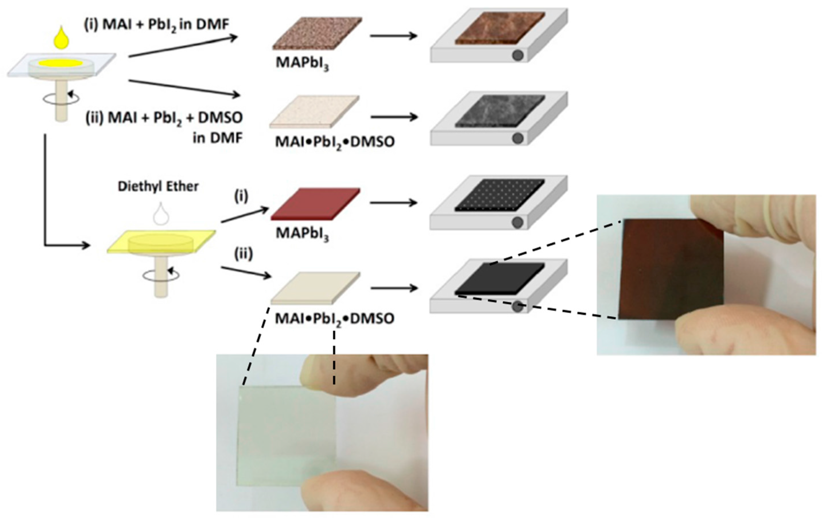
3.4. Anti-Solvent (DE) Dripping Using Precursor Solution Dissolved in DMSO-DMF Mixtures: The Role of the Stable MAI·PbI2·DMSO (1:1:1 mol%) Adduct

The existence of the intermediate MAI·PbI2·DMSO phase was justified by Jeon et al. [8], however it was unclear whether this was indeed a 1:1:1 stoichiometric compound; first because this specific crystalline structure could not be identified by X-ray diffraction, and then because the anti-solvent (TL) is fully miscible with gBL and DMSO, thus some of the DMSO could be washed away during dripping.
To do so, the group of Nam-Gyu Park suggested a novel Lewis acid–base adduct approach. The authors added an equimolar mixture of PbI2, MAI and DMSO (1:1:1 mol%) in DMF. The precursor solution was spin-coated onto the m-TiO2 substrate at 4000 rpm for 25 s. 10 s before the surface changed to be turbid, caused by rapid vaporization of DMF, diethyl ether (DE) was slowly dripped on the rotating substrate. This eventually results in a transparent film that is directly indicative of the formation of the adduct. The purpose of using DE (au lieu of toluene), which is immiscible with DMSO, is to remove only DMF to form the 1:1:1 adduct film; FTIR confirmed the adduct formation. The transparent film is then converted to a dark brown film upon heating at low temperature of 65 °C for 1 min due to removal of the volatile DMSO from the adduct (Figure 3). Average PCEs of 18.3% with a record value of 19.7% were attained via the adduct approach [25].
The approach was adopted by the same group in order to fabricate p-i-n solar cells. For this, perovskite films were deposited on poly(3,4-ethylenedioxythiophene)-poly(styrenesulfonate) or simply called PEDOT:PSS. A best PCE of 18.8% was attained [26]. Interestingly, the method worked also well for typical n-i-p solar cells and, most importantly, for a perovskite with a slightly lower bandgap (than the conventional MAPbI3 perovskite). Wang et al. were able to deposit high quality MA0.7FA0.3PbI3 (where FA stands for formamidinium cation) films on C60 SAM/SnO2 substrates via DE dripping (SAM being a self-assembled monolayer); 2% Pb(SCN)2 was added in order to enhance the crystal grain size. With these, a stabilized PCE of 20.3% was recorded [27]. Likewise, a stabilized PCE of 19% was obtained by depositing the MAPbI3 perovskite via the adduct method onto low temperature UV-treated Nb-doped compact TiO2 substrate [28].

3.5. The Presence of Intermediate Phases: Is 1:1:1 the Correct Molar Ratio for MAI:PbI2:DMSO to Make a Precursor Solution?

Despite the excellent results attained, the exact crystal structure and chemical composition of adduct were in doubt since X-ray diffraction data were missing. Simultaneously with the work of Ahn et al. [25], a very important paper was published, identifying the structure of the intermediate phase as MA2Pb3I8(DMSO)2, using a mixed DMF/DMSO (1:3 v/v) solvent and TL as the anti-solvent (Figure 1a) [29]. It was then suggested that the presence of this specific intermediate was a key point for the formation of a perovskite layer of the desirable morphology [30].
From the above works, an open question unveiled concerning whether the MAI:PbI2:DMSO ratio should remain exactly at 1:1:1 in order to form the MA2Pb3I8(DMSO)2 intermediate. Indeed, Bai et al. systematically manipulated the composition of intermediate perovskite films aiming to optimize the perovskite layer for highly efficient solar cells. By carefully controlling the ratio of DMSO:PbI2 in the perovskite precursor, a pure MA2Pb3I8(DMSO)2 intermediate phase was obtained at the DMSO:PbI2 ratio of 10.0:1 (Figure 4b,c) [31]. In other works, perovskite solar cells prepared by the precursor solution of PbI2:MAI:xDMSO (x = 2.0 [32] or x = 1.5 [33]) exhibited the highest reproducibility and efficiency (compared to the standard 1:1:1 ratio). Quite importantly, the presence of the intermediate was also confirmed during DMSO solvent annealing of a MAPbI3 perovskite film; DMSO vapors react with MAPbI3 to form a MA2Pb3I8(DMSO)2 intermediate at grain boundaries between perovskite crystalline domains. The decomposition of the intermediate can facilitate the grain boundary migration. As a result, the overall crystal size of MAPbI3 crystalline domains increases substantially [34].

3.6. The Unique Case of MAI-Excessive MAPbI3 Perovskite Films

Interestingly, the group of Nam-Gyu Park published a recent work proving that a novel precursor solution containing excess of MAI (e.g., (1 + x)MAI:PbI2:DMSO) was able to introduce an effective passivation layer on the MAPbI3 perovskite grain boundaries (Figure 4d). This grain boundary healing was found to play a crucial role in carrier lifetime improvement, suppression of non-radiative recombination at grain boundaries, and effective extraction of charge carriers at the interface between perovskite and selective contacts. Consequently, the photovoltaic performance was improved, leading to average power conversion efficiencies exceeding 20% at x = 0.06 (recall that average PCEs were 18.3% for x = 0) [35].

3.7. The Importance of the Presence of the Intermediate Phase: A New Era for the Future of Highly-Efficient Perovskite Solar Cells

The discovery of this intermediate species along with the possibility to extend the MAI:PbI2:DMSO ratio into a much wider region motivated lots of researchers to work more closely on anti-solvent crystallization, attempting the fabrication of highly efficient solar cells with a more easily controlled and reproducible manner. Fortunately, this fact has dramatically accelerated the development of perovskite solar cells. In the following figure, we plot PCEs for a large range of highly efficient perovskite solar cells. In the case of pure lead perovskites, we can see that the results are highly reproducible for the solar cells using perovskite films prepared via the intermediate/anti-solvent method. Fourteen independent works have been published, reporting PCEs over 20% (Figure 5a). Other techniques can be similarly efficient; however it is evident that researchers do not prefer to change from anti-solvent treatment. Certainly, we should note here that the current record efficiency (a certified PCE of 22.1%) belongs to a two-step solution process via a triiodide-assisted (through FAI/I2 reaction in IPA) FA+/MA+ intercalation process [36].
Even more importantly, in the case of pure tin or mixed lead/tin perovskite solar cells, anti-solvent crystallization was the sole manner to fabricate films of high quality and excellent surface coverage (Figure 5b). Quite notably, the current record efficiencies (8.1% for pure tin [37] and a certified 17% for 60% tin perovskite [38]) are attained by this technique. We do not intend to comment further on the tin perovskite solar cells here, as we have already published a review paper on the topic [39].

3.8. The Case of PbI2-Excessive Perovskite Films

Getting back to the previous discussion, in full contradiction to the work of Park [35], the groups of Grätzel/Nazeeruddin and Sang Il Seok have published (almost simultaneously) two papers on highly efficient MAPbI3 solar cells based on a non-stoichiometric ratio between PbI2 and MAI precursors (x:1, being x ≥ 1). In the first case, pure DMSO was used as a solvent and CB was dripped during spinning. 10% excessive PbI2 led to efficiencies of 19% under 1 sun illumination [40]. Likewise, Kim et al. adopted the usual gBL/DMSO co-solvent system and TL was utilized as the anti-solvent. 5.7% excess of PbI2 led to optimum results. Interestingly, the approach could be employed for the (FAPbI3)0.85(MAPbBr3)0.15 perovskite as well. This time a DMF/DMSO (6:1 v/v) system dissolved the perovskite constituents and DE was poured onto the substrate. Quite notably, the excess of PbI2 led to slightly smaller grains when compared to pure stoichiometric compound; there was no such effect in the case of MAPbI3 perovskite. The excessive PbI2 perovskite gave a stabilized efficiency of 20.1%, certified at 19.8% [41].
Even though multiple explanations have been suggested in order to interpret the beneficial role of extra PbI2, the most probable cause (in our opinion) should be passivation of grain boundaries (stoichiometric perovskites seem to possess grain boundaries with enriched organic species, impeding charge transport) [42]. Even though these works look completely contradictory to the work of Park [33] (excess of MAI or PbI2 passivates the grain boundaries after all?), we have to notice that, in these works, crystallization occurs via a different road to form the MA2Pb3I8(DMSO)2 intermediate. Therefore, we do not believe that a fair comparison between these two approaches is possible here.

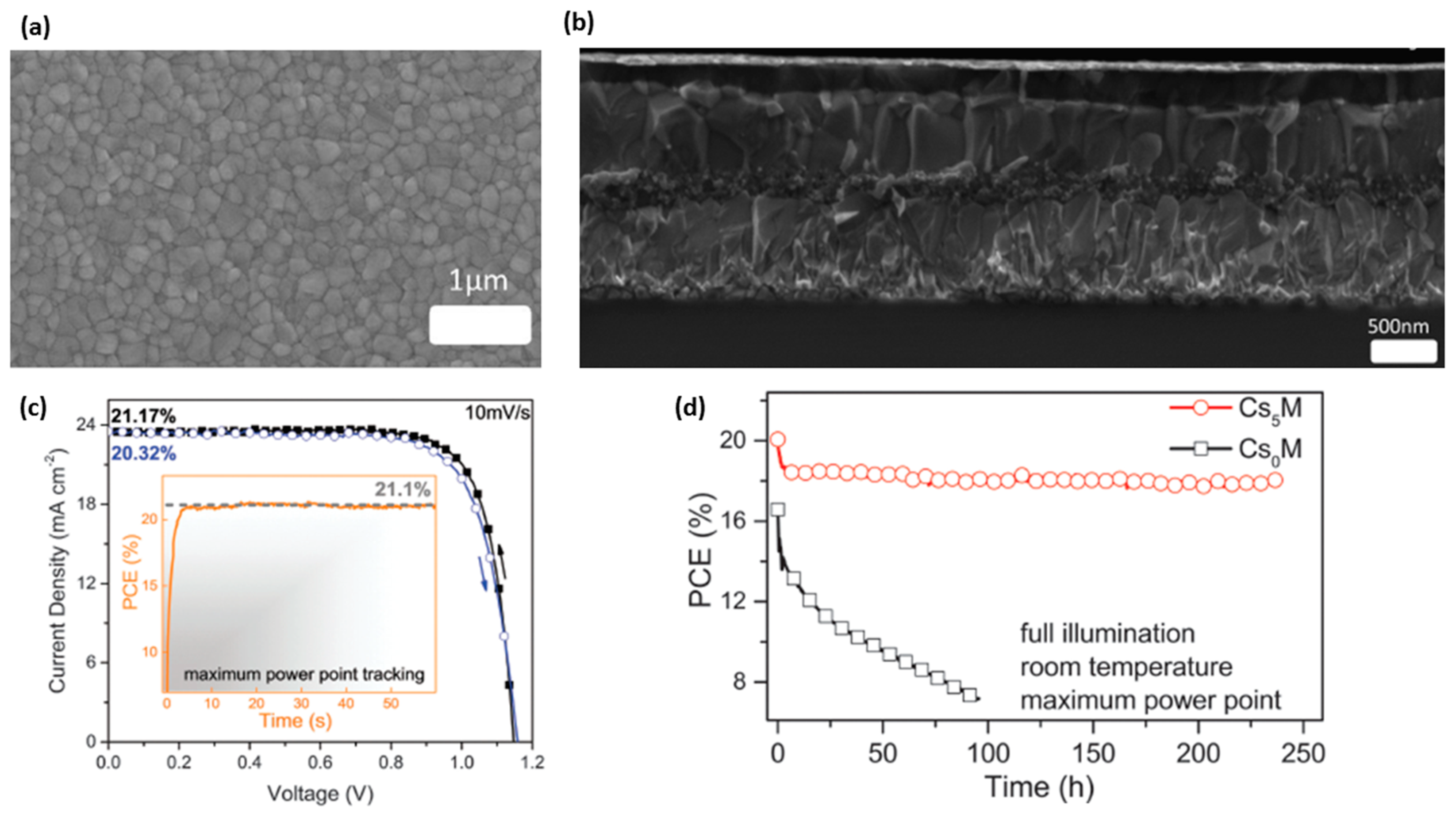
3.9. PbI2-Excessive Perovskite Films: The Key to Attain Record Efficiencies for Mixed Perovskites Grown on a Mesoporous Substrate?

We have previously seen that a PbI2-excessive (FAPbI3)0.85(MAPbBr3)0.15 perovskite could attain PCEs over 20% [41]. This was a motivation for researchers to adopt the approach for various mixed perovskites and enhance further the efficiencies. First, the ~20% efficiencies were confirmed by others [43]. Then, the Grätzel group was able to enhance the efficiency up to 20.8% (with a record open-circuit potential of 1.18 V) by simply optimizing the PbI2:FAI molar ratio at 1.05 [44]. The PCE was further increased up to 21.3% when a thin compositional gradient layer of FAPbBr3−xIx was introduced at the rear interface between the (FAPbI3)0.85(MAPbBr3)0.15 perovskite and the hole transporting material, severely reducing recombination.
Introduction of a small inorganic cation (Cs+) into the perovskite lattice resulted in a triple cation perovskite composition that contained less (yellow) phase impurities and was less sensitive to processing conditions. In our opinion, the key to achieve this was that, after anti-solvent (CB) treatment, films with Cs+ turned dark immediately (i.e., crystallized) after spin coating [45]. Thus, the situation is similar to the classical anti-solvent precipitation; a perovskite is formed when the anti-solvent is injected into the precursor solution (see Section 2.1). Drying is realized then only to drive out the impurities (e.g., CB) and coarsening the film. This was also observed in the case of the intercalation of FAI/MABr/I2 into the initial PbI2/PbBr2 film [36]. We are not aware whether this is happening also due to the involvement of the extra PbI2 in the process. For instance, in the case of the CsxFA(1−x)PbI3 perovskite, Cs incorporation led to small grain sizes, which limited the device performance due to short carrier lifetimes. Addition of 0.5 mol% excess of Pb(SCN)2 was a prerequisite to enlarge the grain size and significantly decrease recombination within the crystal [46]. With this in mind, PCEs of 20.6% were recorded by triple cation perovskites grown on Cs2CO3-treated m-TiO2 substrate [47]. In a seminal work, Saliba et al. managed to fabricate 5 mol% Cs+-doped FAMA films with highly uniform perovskite grains (Figure 6a), extending from the electron to the hole collecting layer, consistent with seed-assisted crystal growth (Figure 6b). Devices could attain record PCEs of 21.2% (under reverse scan,), stabilized at 21.1% (Figure 6c). Interestingly, the devices that incorporated cesium cation in the perovskite film presented a PCE of 18% (at maximum power point) even after 250 h under operational conditions (Figure 6d) [45].
Similar or even better results were drawn when a fourth cation was incorporated into the CsyFA(1−x)MA(1−x−y)PbI3 perovskite lattice. Surprisingly, the Rb+-doped perovskite film had a narrow photoluminescence peak at 770 nm attributable to perovskite, without any further annealing. Thus, the addition of Rb+ (5 mol%) enforces a controllable crystallization and avoids any additional insulating (yellow) phases. With these films, Saliba et al. achieved stabilized efficiencies of up to 21.6% (average value: 20.2%) on small areas (and a stabilized 19.0% on a 0.5 cm2 cell) as well as an electroluminescence of 3.8% [9]. Saliba’s results were independently confirmed by Peng and coworkers who reported a PCE of 20% attained by a meso n-i-p device using a Cs0.07Rb0.03FA0.765MA0.135PbI2.55Br0.45 perovskite. To achieve these large values, the authors incorporated an ultrathin passivation layer, consisting of a mixture of polymethyl(methacrylate), PMMA, and [6,6]-phenyl C61 butyric acid methyl ester (PCBM), on top of the perovskite, effectively passivating defects at or near to the perovskite/TiO2 interface, significantly suppressing interfacial recombination [48].

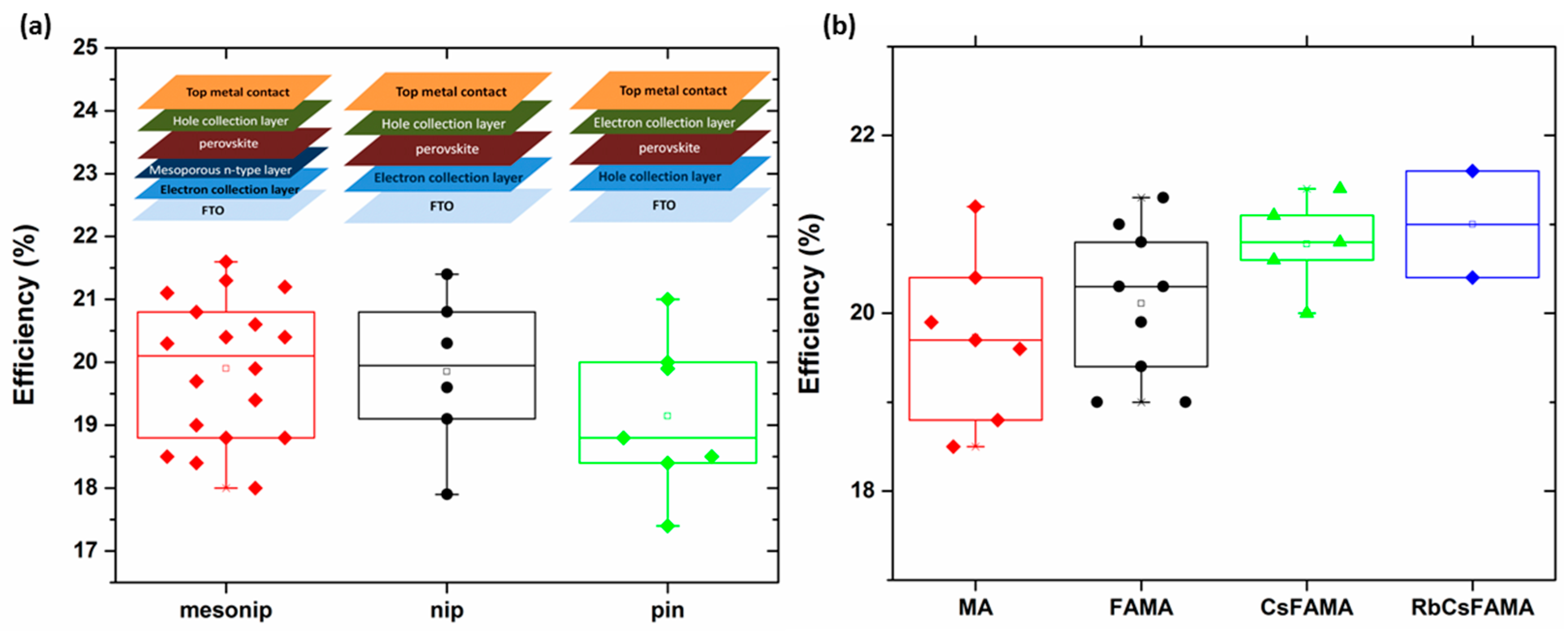
3.10. Mixed Perovskites in n-i-p and p-i-n Solar Cells: Is the Excess of PbI2 a Prerequisite?

Thus, far, almost every work, employing excess of PbI2 in mixed perovskites, referred to meso n-i-p solar cells. There are only two reports on record devices without this concept [23,48]. However, what happens when PbI2-excess concept is applied on n-i-p or p-i-n solar cells?
In the case of the n-i-p devices, stabilized efficiencies of 18% could be attained when a mixed FA(1−x)MAxI(3−y)Bry perovskite was grown onto Mg-doped TiO2 compact layer [49]. By replacing TiO2 with a low temperature SnO2 with higher charge selectivity for efficient electron extraction, a stabilized PCE of 20.8% could be obtained by a Cs+-doped FAMA perovskite [50]. For p-i-n solar cells, (CsPbI3)0.05[(FAPbI3)0.83(MAPbBr3)0.17]0.95 films on top of PTAA led to PCEs of 20% with a fill factor (close to 0.8) approaching the Shockley-Queisser limit [51]. Despite these results, the question remained whether one can fabricate highly efficient, mixed perovskite planar solar cells without an excess of PbI2.
The answer came recently with two breakthrough results. The group of Jinsong Huang published 21% (certified at 20.6%) efficient p-i-n solar cells employing a FA0.85MA0.15Pb(I0.85Br0.15)3 perovskite grown on PTAA substrate via TL dripping/DMSO adduct method. The trick to enhance the efficiencies (from 19.2 up to 21.0%) was to passivate ionic defects at the top surface of the perovskite by choline chloride. With this, the density of states was severely reduced over the whole trap depth region [52]. In the case of n-i-p solar cells, the group of Ted Sargent in Toronto used a chlorine-capped TiO2 layer (au lieu of typical TiO2) as the crystallization substrate, passivating traps and reducing recombination at the interface which forms upon contact of the n-type layer with the Cs0.05FA0.81MA0.14PbI2.55Br0.45 perovskite. Efficiencies of 21.4% were recorded for the best cell, certified at 20.1% [53].
In the following Figure 7a, we compare the efficiencies of various types of solar cells based on MAPbI3 and mixed perovskite films. It is evident that, using a thin mesoporous n-type layer, the efficiencies are very reproducible. However, we should note that record planar (both n-i-p and p-i-n) perovskite solar cells have now reached the values of PCE attained by the meso n-i-p devices. Accidentally or not, these two formulations (FAMA for p-i-n and CsFAMA for n-i-p devices) did not contain an excess of PbI2 (or MAI).
Then, in Figure 7b we show the evolution of the efficiency by simply adding one, two or three cations in the archetypal MAPbI3 lattice. In the case of FAMA perovskites, the bandgap lowers, hence more photocurrent is extracted. For the other two cations (Cs+ and Rb+), a small amount of them (solely 5 mol%), introduced in the lattice, stabilizes the system so that only the pure perovskite phase precipitates out.
Additionally, in Table 1, we summarize all the electrical parameters of the most efficient solar cells, providing a more comprehensive picture of the current status of the literature, concerning various perovskite films (mixed or not) and device structures. With this, one can also have a clearer view on the hysteresis (or not) of the devices (simply, when average PCE is close to stabilized PCE within 1–2%, hysteresis is not an issue).

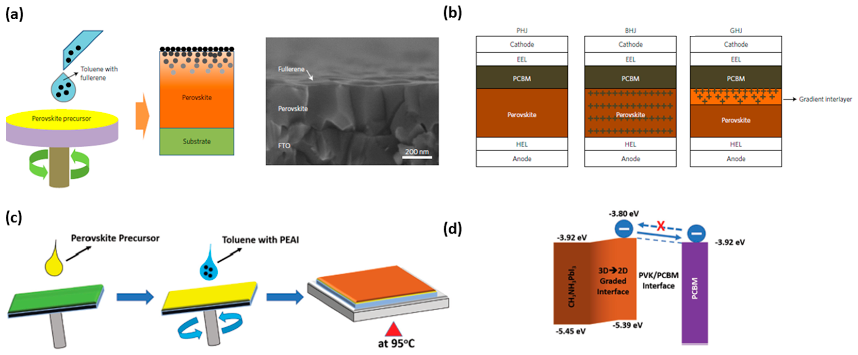
3.11. Dripping Active Compounds at the Top Surface of the Perovskite with the Help of the Anti-Solvent

A year ago, anti-solvent dripping was adopted in order to incorporate active compounds into the perovskite film during its formation. Two papers were published at the same day in Nature Energy. First, a molecular fullerene, PCBM, dissolved in toluene, was dripped onto the MAPbI3 perovskite precursor (dissolved in pure DMSO) film during spinning (Figure 8a). This led to the formation of a mixed interlayer with a gradient of electron acceptors in the perovskite light absorption layer, which was denoted as a graded heterojunction structure (Figure 8b). This structure was found capable of enhancing the PCE of inverted-structured PSCs as it improved the photoelectron collection and reduced recombination loss. With this, certified PCEs exceeding 18%, based on a cell with an aperture area greater than 1 cm2, were obtained [55]. The approach worked really well also in the case of meso n-i-p devices; using a mixed PbI2-excessive FAMA perovskite, efficiencies of 19.9% were recorded [56]. The authors also prepared a fullerene derivative (α-bis-PCBM) through purification of the as-produced PCBM isomer mixture. Quite notably, when α-bis-PCBM replaced standard PCBM in the process, PCE was further increased up to 20.8%. The rationale behind this was that the α-bis-PCBM fulfills (in a better way, compared to PCBM) the vacancies and grain boundaries of the perovskite film, enhancing the crystallization of perovskites and addressing the issue of slow electron extraction. Luckily, α-bis-PCBM also resists the ingression of moisture and passivates voids or pinholes generated in the hole-transporting layer [56].
The second work, published at the same day in Nature Energy, originated from the group of Michael Grätzel at EPFL. The authors adopted the previously reported concept to use an insulating polymer as a template to control nucleation and crystal growth of the perovskite [57]. For this, a PMMA solution in CB/TL (9:1 v/v) was pipetted onto the substrate, 15 s before the end of spin-coating step. Spin-coating was realized at 6500 rpm for 30 s using a typical PbI2-excessive FAMA precursor dissolved in a mixed solvent of DMF, NMP and DMSO (where the molar ratio of DMF/DMSO is 5:1 and the molar ratio of Pb2+/[(DMSO)0.8(NMP)0.2] is 1:1). With this, shiny, smooth perovskite films of excellent electronic quality were obtained, manifested by a remarkably long photoluminescence lifetime. Stable meso n-i-p solar cells with excellent reproducibility were fabricated with record PCEs of up to 21.6% (certified at 21.0%) under standard AM 1.5G illumination conditions [54]. This very interesting concept (polymer-assisted crystallization) gave efficiencies over 20% also in the case of n-i-p MAPbI3 perovskite solar cells (adopting the two step deposition method though) [58].
A unique approach was applied during anti-solvent crystallization by Bai and coworkers [59]. The authors slowly dripped a TL solution of phenethylammonium iodide (PEAI) during spin-coating a MAPbI3 solution in DMF:DMSO (2:7 v/v) co-solvent onto NiO substrate (Figure 8c). PEA+ is a large cation that cannot preserve a 3D perovskite structure; instead, when reacting with PbI2, it forms a 2D PEA2PbI4 perovskite [60].
With this, a 3D-2D (MAPbI3-PEA2Pb2I4) graded perovskite interface is formed, modifying the interface energy levels in such a way that reduces interface charge recombination and simultaneously favors electron extraction (into PCBM electron acceptor) with a marginal resistance (Figure 8d). These properties were translated to PCEs of 19.9% for p-i-n solar cell devices, accompanied with an ultrahigh Voc of 1.17 V. Moreover, benefiting from the large hydrophobic groups at the interface as well as the grain boundaries, the device presented enhanced moisture stability. Additionally, the devices proved to be thermally stable due to suppression of cross-layer ion migration [59]. The fabrication of efficient, ambient-air solar cells with 3D-2D perovskites is a recent trend in literature [61,62,63].
In another approach, electron-deficient aromatic compounds were incorporated at the top surface of perovskite films in order to enhance their photovoltaic performance. More specifically, various nitrogen-containing polycyclic aromatic hydrocarbons, dissolved in DE or CB anti-solvents, were dripped during spin-coating a MAPbI3 solution in DMF:DMSO (10.5:1 v/v) co-solvent onto m-TiO2 substrate. Photoluminescence measurements proved that, upon dripping, non-radiative recombination was severely reduced due to the fact that the organic molecules mainly reside at the grain boundaries of the perovskite films, effectively passivating them [64].

3.12. Various Anti-Solvents Dripping Combined with Adduct Method

Reaching the end of this review, a question evidently comes into the reader’s mind: Why should dripping always involve chlorobenzene, toluene or diethyl ether? What’s wrong with other solvents? In the last part of the review, we will not provide a clear answer but we will briefly discuss the impact of the nature of the anti-solvent on the crystallization process. As far as we are aware of, there are only three reports that compare a whole bunch of poor solvents (for perovskites) that can be used for the process. In two of them, two novel anti-solvents seem to deliver very promising results.
In the first comparative study, Li et al. compared TL, DE and DCM in the crystallization of MAPbI3 (dissolved in pure DMSO) on m-TiO2 substrates. The as-prepared films had very different appearance between each other (Figure 9a), due to the different ratios of MAPbI3 perovskite to MA2Pb3I8(DMSO)2 intermediate phase (recall Figure 4b,c). After annealing, a dense, compact and pinhole free film was obtained only for DE anti-solvent; in both other cases, the films had large, round (DCM) or small sized pinholes (Figure 9b). The authors rationalized the different film formation as follows: when DCM and TL were used as the anti-solvents, DMSO was probably over-extracted and thereby a high content perovskite phase was formed in the as-prepared thin films with more pinholes. On the contrary, in the case of DE, which is immiscible with DMSO, a purer (or more homogeneous) intermediate phase was formed which effectively retards the rapid nucleation. Annealing is not capable of altering the situation when the intermediate phase gradually transforms into the perovskite phase through the intramolecular exchange between DMSO and MAI (Figure 9c). In any event, we have to point out here that all anti-solvents were dripped in an identical way, namely similar volume and dripping rate/time [65].
In the second work, a much larger variety of anti-solvents were dripped on a PbI2-excessive perovskite precursor solution, spin-cast on m-TiO2 substrates (Figure 10a). Interestingly, alcohols such as isobutyl alcohol (IBA) and IPA worked quite efficiently, producing PCEs of 15.8% and 14.8%, respectively. However, the most amazing feature of the work was that ethyl acetate (EA) worked even better than CB, producing pinhole-free films composed of big crystalline grains and reduced number of grain boundaries (Figure 10b). Devices fabricated using the above films, exhibited record PCEs of 19.4%. Again, we should also emphasize the fact that all anti-solvents were dripped in an exactly similar manner [66]. The viability of EA as an anti-solvent was already confirmed by others [67,68,69].
A very concise comparison was recently published by the group of Nazeeruddin at EPFL in Sion. Again lots of solvents were tested, but this time the quantity (of the anti-solvent) and the time of dripping were optimized for every anti-solvent separately. Four of the tested anti-solvents of high boiling point formed perovskite films with a similar grain density and coverage on a nanometer scale; DE-treated films (or not treated at all) have shown pinholes at their surface (Figure 11a).
Interestingly, xylene, which is immiscible with both DMF and DMSO, produced PCEs of 17.8%. However, even better efficiencies were obtained by a new anti-solvent; quite notably, trifluorotoluene (TFL) was proven to give higher PCEs (best at 20.3%) than TL and CB, making it a good candidate for future experiments. We should also notice here that DE produced significantly lower PCEs when compared to rival CB and TL. Finally, the authors suggested a good trick to see whether an anti-solvent is good or bad: one injects the anti-solvent in a vial containing the precursor solution; the formation of the perovskite crystal (brown-blackish precipitate) can be a promising sign for high efficiencies (Figure 11b) [70].
Besides xylene, another solvent (hexane, HX), which is also immiscible with both DMF and DMSO, gave appreciable photovoltaic efficiencies (15.5%). Certainly, these values were increased up to 16.5% when a solvent miscible with DMF (DE) was added in a 50–50 ratio [71]. Another interesting co-solvent system (6% IPA in CB) assisted to get an even higher PCE (19.2%) when dripped on a CsFAMA precursor perovskite film [72]. In the following Figure 12, we summarize all the PCEs attained using various anti-solvents in literature thus far.
Apart from high crystallinity and controllable nucleation/growth kinetics, which result in a polycrystalline film with low defect density, anti-solvent was found to affect the electronic properties of the perovskite. Nawaz et al. evidenced a downward shift of the conduction and valence bands of the MAPbI3 perovskite via toluene-assisted crystallization, leading to favored interfacial charge transfer and consequently to higher open-circuit potential [74]. In turn, Cohen et al. demonstrated, through combined conductive atomic force microscopy and surface photovoltage measurements, that the perovskite film became slightly more intrinsic during TL anti-solvent treatment. They attributed this behavior to the net positive charge on the Pb atoms that is left when halide and methylammonium ions are removed from the surface, resulting in a more conductive surface of the perovskite [75].

4. Summary and Outlook

In summary, we have reviewed all the literature data concerning the intermediate (or adduct)/anti-solvent crystallization method in order to grow (MAPbI3 or mixed) perovskite films of high (and pure) crystallinity and rich substrate coverage; DMSO intermediate with MAI and PbI2 plays a key role to achieve this. Most of the solvents that are poor for perovskites seem to work quite efficiently, irrespectively of miscibility (with DMF, DMSO or both) and boiling point (and vapor pressure) properties. CB, TL and DE are definitely the winning anti-solvents even though TFL and EA have recently shown very interesting results. Meso n-i-p architectures are preferred due to much higher reproducibility and reduced hysteresis, however recent results prove that planar n-i-p and p-i-n devices can reach certified efficiencies of more than 20% as well. Whether a PbI2 or MAI excess in the perovskite precursor solution is a prerequisite or not is still an open question. However, it was clear that adding a second, third or fourth cation into the typical MAPbI3 perovskite, the bandgap lowers delivering more photocurrent (with FA) or a purer perovskite precipitates (with Cs and/or Rb), producing films of excellent electronic quality and record efficiencies.
How can we get at more than 21.6%? Certainly an easy answer is, if we take into account that we are already preparing films of 100% surface coverage, by precipitating a 100% pure polycrystalline perovskite. A trick to this could be an additional washing step after spin-coating (and before annealing) in order to drive away any impurities [68,73,76].
Certainly, the key will be to fully understand the intermediate-to-perovskite transition. Our current understanding is that, in the case of MAPbI3 perovskite, a yellow (e.g., MAI-excessive) intermediate film is enough to produce the perovskite via a simple annealing step for a few min. However, when FA is incorporated, a different lattice is formed and crystallization process could change completely; what is the intermediate that forms then? In any event, dark, well crystalline films should be produced after the end of spin casting.
To conclude, having in mind the recent results obtained by the group of Seok [36], we suspect that researchers will soon attempt to transform the I-deficient [(Pb3I8)n]2n− intermediate into the perovskite via reaction with I2-rich MAI. We argue that efficiency (and stability) increase of solar cell devices will prove to be beneficial for other optoelectronic applications, such as photodetectors, LEDs and X-Ray detectors [11].

Acknowledgments

The current work was funded by the “RESEARCH PROJECTS FOR EXCELLENCE IKY/SIEMENS” and the “IKY FELLOWSHIPS OF EXCELLENCE FOR POSTGRADUATE STUDIES IN GREECE-SIEMENS PROGRAMME” Programmes.

Author Contributions

Thomas Stergiopoulos conceived the topic of this review. Maria Konstantakou wrote the manuscript under the supervision of Thomas Stergiopoulos. Dorothea Perganti and Polycarpos Falaras made comments and revised the manuscript.

Conflicts of Interest

The authors declare no conflict of interest.

References

  1. Kojima, A.; Teshima, K.; Shirai, Y.; Miyasaka, T. Organometal Halide Perovskites as Visible-Light Sensitizers for Photovoltaic Cells. J. Am. Chem. Soc. 2009, 131, 6050–6051. [Google Scholar] [CrossRef] [PubMed]
  2. Lee, M.M.; Teuscher, J.; Miyasaka, T.; Murakami, T.N.; Snaith, H.J. Efficient hybrid solar cells based on meso-superstructured organometal halide perovskites. Science 2012, 338, 643–647. [Google Scholar] [CrossRef] [PubMed]
  3. Kim, H.S.; Lee, C.R.; Im, J.H.; Lee, K.B.; Moehl, T.; Marchioro, A.; Moon, S.J.; Humphry-Baker, R.; Yum, J.H.; Moser, J.E.; et al. Lead iodide perovskite sensitized all-solid-state submicron thin film mesoscopic solar cell with efficiency exceeding 9%. Sci. Rep. 2012, 2, 591. [Google Scholar] [CrossRef] [PubMed]
  4. Heo, J.H.; Im, S.H.; Noh, J.H.; Mandal, T.N.; Lim, C.S.; Chang, J.A.; Lee, Y.H.; Kim, H.J.; Sarkar, A.; Nazeeruddin, M.K.; et al. Efficient inorganic-organic hybrid heterojunction solar cells containing perovskite compound and polymeric hole conductors. Nat. Photonics 2013, 7, 487–492. [Google Scholar] [CrossRef]
  5. Burschka, J.; Pellet, N.; Moon, S.J.; Humphry-Baker, R.; Gao, P.; Nazeeruddin, M.K.; Grätzel, M. Sequential deposition as a route to high-performance perovskite-sensitized solar cells. Nature 2013, 499, 316–319. [Google Scholar] [CrossRef] [PubMed]
  6. Liu, M.; Johnston, M.B.; Snaith, H.J. Efficient planar heterojunction perovskite solar cells by vapour deposition. Nature 2013, 501, 395–398. [Google Scholar] [CrossRef] [PubMed]
  7. Xiao, M.; Huang, F.; Huang, W.; Dkhissi, Y.; Zhu, Y.; Etheridge, J.; Gray-Weale, A.; Bach, U.; Cheng, Y.B.; Spiccia, L.A. Fast deposition-crystallization procedure for highly efficient lead iodide perovskite thin-film solar cells. Angew. Chem. Int. Ed. Engl. 2014, 53, 9898–9903. [Google Scholar] [CrossRef] [PubMed]
  8. Jeon, N.J.; Noh, J.H.; Kim, Y.C.; Yang, W.S.; Ryu, S.; Seok, S.I. Solvent engineering for high-performance inorganic-organic hybrid perovskite solar cells. Nat. Mater. 2014, 13, 897–903. [Google Scholar] [CrossRef] [PubMed]
  9. Saliba, M.; Matsui, T.; Domanski, K.; Seo, J.Y.; Ummadisingu, A.; Zakeeruddin, S.M.; Correa-Baena, J.P.; Tress, W.R.; Abate, A.; Hagfeldt, A.; et al. Incorporation of rubidium cations into perovskite solar cells improves photovoltaic performance. Science 2016, 354, 206–209. [Google Scholar] [CrossRef] [PubMed]
  10. Best Research—Cell Efficiencies. Available online: https://www.nrel.gov/pv/assets/images/efficiency-chart.png (accessed on 27 September 2017).
  11. Zhang, W.; Eperon, G.E.; Snaith, H.J. Metal halide perovskites for energy applications. Nat. Energy 2016, 1, 16048. [Google Scholar] [CrossRef] [Green Version]
  12. Stranks, S.D.; Nayak, P.K.; Zhang, W.; Stergiopoulos, T.; Snaith, H.J. Formation of thin films of organic-inorganic perovskites for high-efficiency solar cells. Angew. Chem. Int. Ed. Engl. 2015, 54, 3240–3248. [Google Scholar] [CrossRef] [PubMed] [Green Version]
  13. Cohen, B.E.; Etgar, L. Parameters that control and influence the organo-metal halide perovskite crystallization and morphology. Front. Optoelectron. 2016, 9, 44–52. [Google Scholar] [CrossRef]
  14. Lee, J.W.; Kim, H.S.; Park, N.G. Lewis acid–base adduct approach for high efficiency perovskite solar cells. Acc. Chem. Res. 2016, 49, 311–319. [Google Scholar] [CrossRef] [PubMed]
  15. Seo, J.; Noh, J.H.; Il Seok, S. Rational strategies for efficient perovskite solar cells. Acc. Chem. Res. 2016, 49, 562–572. [Google Scholar] [CrossRef] [PubMed]
  16. Chen, Y.; He, M.; Peng, J.; Sun, Y.; Liang, Z. Structure and growth control of organic–inorganic halide perovskites for optoelectronics: From polycrystalline films to single crystals. Adv. Sci. 2016, 3, 1500392. [Google Scholar] [CrossRef] [PubMed]
  17. Fakharuddin, A.; Schmidt-Mende, L.; Garcia-Belmonte, G.; Jose, R.; Mora-Sero, I. Interfaces in perovskite solar cells. Adv. Energy Mater. 2017, 65, 1700623. [Google Scholar] [CrossRef]
  18. Snaith, H.J.; Abate, A.; Ball, J.M.; Eperon, G.E.; Leijtens, T.; Noel, N.K.; Stranks, S.D.; Wang, J.T.W.; Wojciechowski, K.; Zhang, W. Anomalous hysteresis in perovskite solar cells. J. Phys. Chem. Lett. 2014, 5, 1511–1515. [Google Scholar] [CrossRef] [PubMed]
  19. Saidaminov, M.I.; Abdelhady, A.L.; Murali, B.; Alarousu, E.; Burlakov, V.M.; Peng, W.; Dursun, I.; Wang, L.; He, Y.; Maculan, G.; et al. High-quality bulk hybrid perovskite single crystals within minutes by inverse temperature crystallization. Nat. Commun. 2015, 6, 7586. [Google Scholar] [CrossRef] [PubMed]
  20. Stoumpos, C.C.; Malliakas, C.D.; Kanatzidis, M.G. Semiconducting tin and lead iodide perovskites with organic cations: Phase transitions, high mobilities, and near-infrared photoluminescent properties. Inorg. Chem. 2013, 52, 9019–9038. [Google Scholar] [CrossRef] [PubMed]
  21. Tidhar, Y.; Edri, E.; Weissman, H.; Zohar, D.; Hodes, G.; Cahen, D.; Rybtchinski, B.; Kirmayer, S. Crystallization of methyl ammonium lead halide perovskites: Implications for photovoltaic applications. J. Am. Chem. Soc. 2014, 136, 13249–13256. [Google Scholar] [CrossRef] [PubMed]
  22. Shi, D.; Adinolfi, V.; Comin, R.; Yuan, M.; Alarousu, E.; Buin, A.; Chen, Y.; Hoogland, S.; Rothenberger, A.; Katsiev, K.; et al. Low trap-state density and long carrier diffusion in organolead trihalide perovskite single crystals. Science 2015, 347, 519–522. [Google Scholar] [CrossRef] [PubMed]
  23. Shin, S.S.; Yeom, E.J.; Yang, W.S.; Hur, S.; Kim, M.G.; Im, J.; Seo, J.; Noh, J.H.; Il Seok, S. Colloidally prepared La-doped BaSnO3 electrodes for efficient, photostable perovskite solar cells. Science 2017, 356, 167–171. [Google Scholar] [CrossRef] [PubMed]
  24. Yang, M.; Zhang, T.; Schulz, P.; Li, Z.; Li, G.; Kim, D.H.; Guo, N.; Berry, J.J.; Zhu, K.; Zhao, Y. Facile fabrication of large-grain CH3NH3PbI3−xBrx films for high-efficiency solar cells via CH3NH3Br selective Ostwald ripening. Nat. Commun. 2016, 7, 12305. [Google Scholar] [CrossRef] [PubMed]
  25. Ahn, N.; Son, D.Y.; Jang, I.H.; Min, K.S.; Choi, M.; Park, N.G. Highly reproducible perovskite solar cells with average efficiency of 18.3% and best efficiency of 19.7% fabricated via lewis base adduct of lead(ii) iodide. J. Am. Chem. Soc. 2015, 137, 8696–8699. [Google Scholar] [CrossRef] [PubMed]
  26. Sung, H.; Ahn, N.; Jang, M.S.; Lee, J.K.; Yoon, H.; Park, N.G.; Choi, M. Transparent conductive oxide-free graphene-based perovskite solar cells with over 17% efficiency. Adv. Energy Mater. 2015, 6, 1501873. [Google Scholar] [CrossRef]
  27. Wang, C.; Xiao, C.; Yu, Y.; Zhao, D.; Awni, R.A.; Grice, C.R.; Ghimire, K.; Constantinou, D.; Liao, W.; Cimaroli, A.J.; et al. Understanding and eliminating hysteresis for highly efficient planar perovskite solar cells. Adv. Energy Mater. 2017, 1700414. [Google Scholar] [CrossRef]
  28. Jeong, I.; Jung, H.; Park, M.; Park, J.S.; Hae, J.; Joo, J.; Lee, J.; Ko, M.J. A tailored TiO2 electron selective layer for high-performance flexible perovskite solar cells via low temperature UV process. Nano Energy 2016, 28, 380–389. [Google Scholar] [CrossRef]
  29. Rong, Y.; Tang, Z.; Zhao, Y.; Zhong, X.; Venkatesan, S.; Graham, H.; Patton, M.; Jing, Y.; Guloy, A.M.; Yao, Y. Solvent engineering towards controlled grain growth in perovskite planar heterojunction solar cells. Nanoscale 2015, 7, 10595–10599. [Google Scholar] [CrossRef] [PubMed]
  30. Rong, Y.; Venkatesan, S.; Guo, R.; Wang, Y.; Bao, J.; Li, W.; Fan, Z.; Yao, Y. Critical kinetic control of non-stoichiometric intermediate phase transformation for efficient perovskite solar cells. Nanoscale 2016, 8, 12892–12899. [Google Scholar] [CrossRef] [PubMed]
  31. Bai, Y.; Xiao, S.; Hu, C.; Zhang, T.; Meng, X.; Li, Q.; Yang, Y.; Wong, K.S.; Chen, H.; Yang, S. A pure and stable intermediate phase is key to growing aligned and vertically monolithic perovskite crystals for efficient PIN planar perovskite solar cells with high processibility and stability. Nano Energy 2017, 34, 58–68. [Google Scholar] [CrossRef]
  32. Tu, Y.; Wu, J.; He, X.; Guo, P.; Luo, H.; Liu, Q.; Lin, J.; Huang, M.; Huang, Y.; Fan, L.; et al. Controlled growth of CH3NH3PbI3 films towards efficient perovskite solar cells by varied-stoichiometric intermediate adduct. Appl. Surf. Sci. 2017, 403, 572–577. [Google Scholar] [CrossRef]
  33. Ren, Y.K.; Liu, S.D.; Duan, B.; Xu, Y.F.; Li, Z.Q.; Huang, Y.; Hu, L.H.; Zhu, J.; Dai, S.Y. Controllable intermediates by molecular self-assembly for optimizing the fabrication of large-grain perovskite films via one-step spin-coating. J. Alloy. Compd. 2017, 705, 205–210. [Google Scholar] [CrossRef]
  34. Xiao, S.; Bai, Y.; Meng, X.; Zhang, T.; Chen, H.; Zheng, X.; Hu, C.; Qu, Y.; Yang, S. Unveiling a key intermediate in solvent vapor post-annealing to enlarge crystalline domains of organometal halide perovskite films. Adv. Funct. Mater. 2017, 27, 1604944. [Google Scholar] [CrossRef]
  35. Son, D.Y.; Lee, J.W.; Choi, Y.J.; Jang, I.H.; Lee, S.; Yoo, P.J.; Shin, H.; Ahn, N.; Choi, M.; Kim, D.; et al. Self-formed grain boundary healing layer for highly-efficient CH3NH3PbI3 perovskite solar cells. Nat. Energy 2016, 1, 16081. [Google Scholar] [CrossRef]
  36. Yang, W.S.; Park, B.W.; Jung, E.H.; Jeon, N.J.; Kim, Y.C.; Lee, D.U.; Shin, S.S.; Seo, J.; Kim, E.K.; Noh, J.H.; et al. Iodide management in formamidinium-lead-halide–based perovskite layers for efficient solar cells. Science 2017, 356, 1376. [Google Scholar] [CrossRef] [PubMed]
  37. Zhao, Z.; Gu, F.; Li, Y.; Sun, W.; Ye, S.; Rao, H.; Liu, Z.; Bian, Z.; Huang, C. Mixed-Organic-Cation tin iodide for lead-free perovskite solar cells with an efficiency of 8.12%. Adv. Sci. 2017, 131, 1700204. [Google Scholar] [CrossRef]
  38. Zhao, D.; Yu, Y.; Wang, C.; Liao, W.; Shrestha, N.; Grice, C.R.; Cimaroli, A.J.; Lei, G.; Ellingson, R.J.; Zhu, K.; et al. Low-bandgap mixed tin–lead iodide perovskite absorbers with long carrier lifetimes for all-perovskite tandem solar cells. Nat. Energy 2017, 2, 17018. [Google Scholar] [CrossRef]
  39. Konstantakou, M.; Stergiopoulos, T. A critical review on tin halide perovskite solar cells. J. Mater. Chem. A 2017, 5, 11518–11549. [Google Scholar] [CrossRef]
  40. Roldán-Carmona, C.; Gratia, P.; Zimmermann, I.; Grancini, G.; Gao, P.; Graetzel, M.; Nazeeruddin, M.K. High efficiency methylammonium lead triiodide perovskite solar cells: The relevance of non-stoichiometric precursors. Energy Environ. Sci. 2015, 8, 3550–3556. [Google Scholar] [CrossRef]
  41. Kim, Y.C.; Jeon, N.J.; Noh, J.H.; Yang, W.S.; Seo, J.; Yun, J.; Ho-Baillie, A.; Huang, S.; Green, M.A.; Seidel, J.; et al. Beneficial effects of PBI2 incorporated in organo-lead halide perovskite solar cells. Adv. Energy Mater. 2016, 6, 1502104. [Google Scholar] [CrossRef]
  42. Jacobsson, T.J.; Correa-Baena, J.P.; Anaraki, E.H.; Philippe, B.; Stranks, S.D.; Bouduban, M.E.F.; Tress, W.; Schenk, K.; Teuscher, J.; Moser, J.E.; et al. Unreacted PbI2 as a double-edged sword for enhancing the performance of perovskite solar cells. J. Am. Chem. Soc. 2016, 138, 10331–10343. [Google Scholar] [CrossRef] [PubMed]
  43. Xie, L.Q.; Chen, L.; Nan, Z.A.; Lin, H.X.; Wang, T.; Zhan, D.; Yan, J.W.; Mao, B.W.; Tian, Z.Q. Understanding the cubic phase stabilization and crystallization kinetics in mixed cations and halides perovskite single crystals. J. Am. Chem. Soc. 2017, 139, 3320–3323. [Google Scholar] [CrossRef] [PubMed]
  44. Bi, D.; Tress, W.M.; Dar, I.; Gao, P.; Luo, J.; Renevier, C.; Schenk, K.; Abate, A.; Giordano, F.; Correa Baena, J.P.; et al. Efficient luminescent solar cells based on tailored mixed-cation perovskites. Sci. Adv. 2016, 2, 1501170. [Google Scholar] [CrossRef] [PubMed]
  45. Saliba, M.; Matsui, T.; Seo, J.Y.; Domanski, K.; Correa-Baena, J.P.; Nazeeruddin, M.K.; Zakeeruddin, S.M.; Tress, W.; Abate, A.; Hagfeldt, A.; et al. Cesium-containing triple cation perovskite solar cells: Improved stability, reproducibility and high efficiency. Energy Environ. Sci. 2016, 9, 1989–1997. [Google Scholar] [CrossRef] [PubMed]
  46. Yu, Y.; Wang, C.; Grice, C.R.; Shrestha, N.; Chen, J.; Zhao, D.; Liao, W.; Cimaroli, A.J.; Roland, P.J.; Ellingson, R.J.; et al. Improving the performance of formamidinium and cesium lead triiodide perovskite solar cells using lead thiocyanate additives. ChemSusChem 2016, 9, 3288–3297. [Google Scholar] [CrossRef] [PubMed]
  47. Ye, T.; Petrović, M.; Peng, S.; Yoong, J.L.K.; Vijila, C.; Ramakrishna, S. Enhanced charge carrier transport and device performance through dual-cesium doping in mixed-cation perovskite solar cells with near unity free carrier ratios. ACS Appl. Mater. Interfaces 2017, 9, 2358–2368. [Google Scholar] [CrossRef] [PubMed]
  48. Peng, J.; Wu, Y.; Ye, W.; Jacobs, D.A.; Shen, H.; Fu, X.; Wan, Y.; Duong, T.; Wu, N.; Barugkin, C.; et al. Interface passivation using ultrathin polymer–fullerene films for high-efficiency perovskite solar cells with negligible hysteresis. Energy Environ. Sci. 2017, 10, 1792–1800. [Google Scholar] [CrossRef]
  49. Zhang, H.; Shi, J.; Xu, X.; Zhu, L.; Luo, Y.; Li, D.; Meng, Q. Mg-doped TiO2 boosts the efficiency of planar perovskite solar cells to exceed 19%. J. Mater. Chem. A 2016, 4, 15383–15389. [Google Scholar] [CrossRef]
  50. Anaraki, E.H.; Kermanpur, A.; Steier, L.; Domanski, K.; Matsui, T.; Tress, W.; Saliba, M.; Abate, A.; Grätzel, M.; Hagfeldt, A.; et al. Highly efficient and stable planar perovskite solar cells by solution-processed tin oxide. Energy Environ. Sci. 2016, 9, 3128–3134. [Google Scholar] [CrossRef]
  51. Stolterfoht, M.; Wolff, C.M.; Amir, Y.; Paulke, A.; Perdigón-Toro, L.; Caprioglio, P.; Neher, D. Approaching the fill factor Shockley–Queisser limit in stable, dopant-free triple cation perovskite solar cells. Energy Environ. Sci. 2017, 10, 1530–1539. [Google Scholar] [CrossRef]
  52. Zheng, X.; Chen, B.; Dai, J.; Fang, Y.; Bai, Y.; Lin, Y.; Wei, H.; Zeng, X.C.; Huang, J. Defect passivation in hybrid perovskite solar cells using quaternary ammonium halide anions and cations. Nat. Energy 2017, 2, 17102. [Google Scholar] [CrossRef]
  53. Tan, H.; Jain, A.; Voznyy, O.; Lan, X.; de Arquer, F.P.G.; Fan, J.Z.; Quintero-Bermudez, R.; Yuan, M.; Zhang, B.; Zhao, Y.; et al. Efficient and stable solution-processed planar perovskite solar cells via contact passivation. Science 2017, 355, 722–726. [Google Scholar] [CrossRef] [PubMed]
  54. Bi, D.; Yi, C.; Luo, J.; Décoppet, J.D.; Zhang, F.; Zakeeruddin, S.M.; Li, X.; Hagfeldt, A.; Grätzel, M. Polymer-templated nucleation and crystal growth of perovskite films for solar cells with efficiency greater than 21%. Nat. Energy 2016, 1, 16142. [Google Scholar] [CrossRef]
  55. Wu, Y.; Yang, X.; Chen, W.; Yue, Y.; Cai, M.; Xie, F.; Bi, E.; Islam, A.; Han, L. Perovskite solar cells with 18.21% efficiency and area over 1 cm2 fabricated by heterojunction engineering. Nat. Energy 2016, 1, 16148. [Google Scholar] [CrossRef]
  56. Zhang, F.; Shi, W.; Luo, J.; Pellet, N.; Yi, C.; Li, X.; Zhao, X.; Dennis, T.J.S.; Li, X.; Wang, S.; et al. Isomer-pure bis-pcbm-assisted crystal engineering of perovskite solar cells showing excellent efficiency and stability. Adv. Mater. 2017, 29, 1606806. [Google Scholar] [CrossRef] [PubMed]
  57. Zhao, Y.; Wei, J.; Li, H.; Yan, Y.; Zhou, W.; Yu, D.; Zhao, Q. A polymer scaffold for self-healing perovskite solar cells. Nat. Commun. 2016, 7, 10228. [Google Scholar] [CrossRef] [PubMed]
  58. Zuo, L.; Guo, H.; de Quilettes, D.W.; Jariwala, S.; de Marco, N.; Dong, S.; de Block, R.; Ginger, D.S.; Dunn, B.; Wang, M.; et al. Polymer-modified halide perovskite films for efficient and stable planar heterojunction solar cells. Sci. Adv. 2017, 3. [Google Scholar] [CrossRef] [PubMed]
  59. Bai, Y.; Xiao, S.; Hu, C.; Zhang, T.; Meng, X.; Lin, H.; Yang, Y.; Yang, S. Dimensional engineering of a graded 3d–2d halide perovskite interface enables ultrahigh voc enhanced stability in the p-i-n photovoltaics. Adv. Energy Mater. 2017, 1701038. [Google Scholar] [CrossRef]
  60. Mitzi, D.B.; Field, C.A.; Harrison, W.T.A.; Guloy, A.M. Conducting tin halides with a layered organic-based perovskite structure. Nature 1994, 369, 467. [Google Scholar] [CrossRef]
  61. Grancini, G.; Roldán-Carmona, C.; Zimmermann, I.; Mosconi, E.; Lee, X.; Martineau, D.; Narbey, S.; Oswald, F.; de Angelis, F.; Graetzel, M.; et al. One-Year stable perovskite solar cells by 2D/3D interface engineering. Nat. Commun. 2017, 8, 15684. [Google Scholar] [CrossRef] [PubMed]
  62. Li, N.; Zhu, Z.; Chueh, C.C.; Liu, H.; Peng, B.; Petrone, A.; Li, X.; Wang, L.; Jen, A.K.Y. Mixed cation FAxPEA1–xPbI3 with enhanced phase and ambient stability toward high-performance perovskite solar cells. Adv. Energy Mater. 2017, 7, 1601307. [Google Scholar] [CrossRef]
  63. Wang, Z.; Lin, Q.; Chmiel, F.P.; Sakai, N.; Herz, L.M.; Snaith, H.J. Efficient ambient-air-stable solar cells with 2D–3D heterostructured butylammonium-caesium formamidinium lead halide perovskites. Nat. Energy. 2017, 6, 17135. [Google Scholar] [CrossRef]
  64. Ngo, T.T.; Suarez, I.; Antonicelli, G.; Cortizo-Lacalle, D.; Martinez-Pastor, J.P.; Mateo-Alonso, A.; Mora-Sero, I. Enhancement of the performance of perovskite solar cells, LEDs, and optical amplifiers by anti-solvent additive deposition. Adv. Mater. 2017, 29, 1604056. [Google Scholar] [CrossRef] [PubMed]
  65. Li, Y.; Wang, J.; Yuan, Y.; Dong, X.; Wang, P. Anti-solvent dependent device performance in CH3NH3PbI3 solar cells: The role of intermediate phase content in the as-prepared thin films. Sustain. Energy Fuels 2017, 1, 1041–1048. [Google Scholar] [CrossRef]
  66. Bu, T.; Wu, L.; Liu, X.; Yang, X.; Zhou, P.; Yu, X.; Qin, T.; Shi, J.; Wang, S.; Li, S.; et al. Synergic interface optimization with green solvent engineering in mixed perovskite solar cells. Adv. Energy Mater. 2017, 1700576. [Google Scholar] [CrossRef]
  67. Yin, M.; Xie, F.; Chen, H.; Yang, X.; Ye, F.; Bi, E.; Wu, Y.; Cai, M.; Han, L. Annealing-free perovskite films by instant crystallization for efficient solar cells. J. Mater. Chem. A 2016, 4, 8548–8553. [Google Scholar] [CrossRef]
  68. Fei, C.; Li, B.; Zhang, R.; Fu, H.; Tian, J.; Cao, G. Highly efficient and stable perovskite solar cells based on monolithically grained ch3nh3pbi3 film. Adv. Energy Mater. 2017, 1602017. [Google Scholar] [CrossRef]
  69. Troughton, J.; Hooper, K.; Watson, T.M. Humidity resistant fabrication of CH3NH3PbI3 perovskite solar cells and modules. Nano Energy 2017, 39, 60–68. [Google Scholar] [CrossRef]
  70. Paek, S.; Schouwink, P.; Athanasopoulou, E.N.; Cho, K.T.; Grancini, G.; Lee, Y.; Zhang, Y.; Stellacci, F.; Nazeeruddin, M.K.; Gao, P. From nano to micrometer scale: The role of anti-solvent treatment on the high-performance perovskite solar cells. Chem. Mater. 2017, 29, 3490–3498. [Google Scholar] [CrossRef]
  71. Yu, Y.; Yang, S.; Lei, L.; Cao, Q.; Shao, J.; Zhang, S.; Liu, Y. Ultrasmooth perovskite film via mixed anti-solvent strategy with improved efficiency. ACS Appl. Mater. Interfaces 2017, 9, 3667–3676. [Google Scholar] [CrossRef] [PubMed]
  72. Wang, Y.; Wu, J.; Zhang, P.; Liu, D.; Zhang, T.; Ji, L.; Gu, X.; Chen, Z.D.; Li, S. Stitching triple cation perovskite by a mixed anti-solvent process for high performance perovskite solar cells. Nano Energy 2017, 39, 616–625. [Google Scholar] [CrossRef]
  73. Eperon, G.E.; Leijtens, T.; Bush, K.A.; Prasanna, R.; Green, T.; Wang, J.T.W.; McMeekin, D.P.; Volonakis, G.; Milot, R.L.; May, R.; et al. Perovskite-perovskite tandem photovoltaics with optimized band gaps. Science 2016, 354, 861–865. [Google Scholar] [CrossRef] [PubMed]
  74. Nawaz, A.; Erdinc, A.K.; Gultekin, B.; Tayyib, M.; Zafer, C.; Wang, K.; Akram, M.N.; Wong, K.K.; Hussain, S.; Schmidt-Mende, L.; et al. Insights into optoelectronic properties of anti-solvent treated perovskite films. J. Mater. Sci. Mater. Electron. 2017, 1–7. [Google Scholar] [CrossRef]
  75. Cohen, B.E.; Aharon, S.; Dymshits, A.; Etgar, L. Impact of antisolvent treatment on carrier density in efficient hole-conductor-free perovskite-based solar cells. J. Phys. Chem. C 2016, 120, 142–147. [Google Scholar] [CrossRef]
  76. Cao, J.; Jing, X.; Yan, J.; Hu, C.; Chen, R.; Yin, J.; Li, J.; Zheng, N. Identifying the molecular structures of intermediates for optimizing the fabrication of high-quality perovskite films. J. Am. Chem. Soc. 2016, 138, 9919–9926. [Google Scholar] [CrossRef] [PubMed]
Figure 1. (a) A schematic diagram of a typical, anti-solvent crystallization process for MAPbI3 perovskite formation. (b) A vial containing an orange single crystal of MAPbBr3, grown by the anti-solvent (IPA) crystallization method and optical microscope image of the crystal. Reprinted with permission from [21]. Copyright (2014) American Chemical Society.
Crystals 07 00291 g001
Figure 2. (a) Schematic illustration of anti-solvent dripping (denoted as FDC) and conventional spin-coating process for fabricating perovskite films. Conventional spin-coating (top) results in a gray film (on top of a compact TiO2 layer) composed of rod-like crystals. In the FDC process (bottom), a light brown film is formed, consisting of uniformly sized perovskite grains. (b) SEM images of the surface morphology of films prepared by adding CBZ at different delay times from the start of the spin-coating process (after 2 s and 8 s) Note that a delay time between 4 and 6 s produces the optimum morphology. Reproduced from Ref. [7] with permission from Wiley-VCH. (c) Toluene dripping during precursor perovskite solution (gBL-DMSO) spin-casting onto m-TiO2 substrate for preparing a stable intermediate which easily transforms into the perovskite after annealing. Reproduced from ref. [8] with permission from Nature Publishing Group.
Crystals 07 00291 g002
Figure 3. Schematic representation of the anti-solvent (DE) dripping method when incorporating or not DMSO as a co-solvent in the perovskite precursor solution. Macroscopical photos of the films in the intermediate (transparent) and perovskite phase (dark brown) are also shown. Perovskite is formed after annealing at 65 °C for 1 min and then at 100 °C for 2 min. [25]. Copyright (2015) American Chemical Society.
Crystals 07 00291 g003
Figure 4. (a) The schematic crystal structure and composition of the intermediate MA2Pb3I8(DMSO)2 phase. Reprinted from [30] with permission from Royal Society of Chemistry. (b) Photos of different intermediate films on NiO substrates based on precursor solutions varying the DMF/DMSO volume ratio. Toluene is adopted as an anti-solvent here. Note that a transparent film appears in the case of DMSO:PbI2 4.2:1 (while the transparent film of Figure 3 shows up at a 1:1 molar ratio when DE is dripped during spinning), highlighting the importance of the anti-solvent being used (the substrate also should play a role here). (c) Schematic illustrating the relation between the amount of DMSO and the component of intermediate film. Note that the best results (photovoltaic efficiencies) were obtained after conversion of the yellow film (DMSO:PbI2 = 10:1) into a perovskite through annealing at 95 °C for 30 min. Reprinted from [31] with permission from Elsevier. (d) By adding excess of CH3NH3I in the precursor solution, a yellowish intermediate film was prepared which was later converted to a perovskite film with self-formed grain boundaries (top SEM view image). These films led to champion photovoltaic efficiencies (average PCEs over 20%) for a CH3NH3PbI3 perovskite. Reproduced from Ref. [35] with permission from Nature Publishing Group.
Crystals 07 00291 g004
Figure 5. Overall photovoltaic efficiencies of (various types of) perovskite solar cells with perovskite films fabricated via a combined intermediate/anti-solvent crystallization method: (a) solar cells based on pure Pb2+ perovskite and (b) solar cells based on mixed Pb/Sn perovskites. Note that in the case of pure lead perovskite solar cells, only efficiencies higher than 18.5% were introduced in the statistical analysis. Data were taken from the references existing in the present manuscript.
Crystals 07 00291 g005
Figure 6. (a) Top (b) and cross-sectional view scanning electron microscope (SEM) images of the Cs-doped FAMA perovskite films and the whole meso n-i-p devices, respectively. (c) Forward and reverse scanned J-V curves under 1 sun illumination and stabilized output power characteristics recorded for 60 s. (d) Aging for 250 h of devices with (Cs5M) or without Cs+ (Cs0M) in a nitrogen atmosphere held at room temperature under constant illumination and maximum power point tracking [45]. Published by The Royal Society of Chemistry.
Crystals 07 00291 g006
Figure 7. Overall photovoltaic efficiencies of perovskite solar cells with various mixed (or not) perovskite films fabricated via a combined intermediate/anti-solvent crystallization method: (a) mesonip, nip and pin cells refer to a specific architecture depicted in the figure as an inset. See text for further details. (b) MA, FAMA, CsFAMA and RbCsFAMA refer to compounds consisting of pure MAPbI3, mixed FAPbI3-MAPbI3, Cs+-doped mixed FAPbI3-MAPbI3 and Rb+/Cs+-co-doped mixed FAPbI3-MAPbI3, respectively. Note that various types (meso n-i-p, n-i-p and p-i-n) of highly efficient (over 18.5%) solar cells are included in the statistical analysis. Data were taken from the references existing in the present manuscript.
Crystals 07 00291 g007
Figure 8. (a) A schematic of the method of depositing fullerene molecules at the very top surface of the perovskite along with a cross-sectional SEM image of the dripping-induced perovskite–PCBM stacking. (b) Schematic of the p-i-n solar cell depicting the formation of a graded heterojunction, GHJ (perovskite with a gradient distribution of PCBM), in comparison with typical planar (PHJ) and bulk heterojunction (BHJ) devices. Reproduced from Ref. [55] with permission from Nature Publishing Group. (c) The schematic of the 3D-2D perovskite deposition. (d) Schematic of energy level alignment at the 3D-2D perovskite and PCBM interface. Reproduced from Ref [59] with permission from Wiley-VCH.
Crystals 07 00291 g008
Figure 9. (a) Photographs of the as-prepared perovskite films using different anti-solvents. (b) SEM images of the same films after annealing. (c) Schematic illustration for the formation process of the perovskite films via the intermediate/anti-solvent approach. Reproduced from Ref. [65] with permission from Royal Society of Chemistry.
Crystals 07 00291 g009
Figure 10. (a) Photographs of perovskite films fabricated using different anti-solvents before (the top brown one) and after annealing (the bottom black one) (b) Top view SEM images of the EA-processed perovskite films after annealing. Reproduced from Ref. [66] with permission from Wiley-VCH.
Crystals 07 00291 g010
Figure 11. (a) SEM images of perovskite films treated (or not) by various anti-solvents (trifluorotoluene: FTL, toluene:TL, chlorobenzene: CB, xylene: XYL, diethyl ether: DE); (b) Photograph of adding anti-solvents into precursor solutions. Reproduced from Ref. [70] with permission from American Chemical Society.
Crystals 07 00291 g011
Figure 12. Overall photovoltaic efficiencies of various types of solar cells which use perovskite films fabricated by the application of different anti-solvents in the combined intermediate/anti-solvent crystallization method. Note that in the case of anisole (AN), a highly efficient solar cell based on a Pb/Sn mixed perovskite [73] was included in the analysis.
Crystals 07 00291 g012
Table 1. Parameters for solar cells (measured at 1 sun-AM1.5G) based on record-efficient perovskite solar cells (adopting various n- or p-type contacts and under various cell structures). Jsc, Voc and FF values are taken from the best device, reported in every reference.
PerovskiteDevice StructureJsc (mA cm−2)Voc (V)FFAverage PCE (%)Stabilized PCE (%) Certified PCE (%) Reference
MAPbI3Meso n-i-p23.71.120.7820.1>20-[35]
FAMAMeso n-i-p23.71.140.7821.0-21.0[54]
FAMAMeso n-i-p23.41.120.8120.3-21.2[23]
FAMAp-i-n23.71.140.7819.419.620.6[52]
CsFAMAn-i-p22.31.190.8119.820.920.1[53]
RbCsFAMAMeso n-i-p22.81.180.8120.221.6-[9]

