Article

Deep-Blue Organic Light-Emitting Diodes Employed Traditional Hole Transporting Material as Emitter for 31-Inch 4K Flexible Display

1
School of Electronic and Communication Engineering, Shenzhen Polytechnic, Shenzhen 518000, China
2
Materials Science and Engineering, Tianjin University, Tianjin 300072, China
3
Ningbo Weierskeller Intelligent Technology Co., Ltd., Ningbo 315210, China
4
School of Foreign Languages and Trade, Guangzhou City Construction College, Guangzhou 510006, China
*
Authors to whom correspondence should be addressed.
Crystals 2023, 13(4), 687; https://doi.org/10.3390/cryst13040687
Submission received: 22 February 2023 / Revised: 9 April 2023 / Accepted: 14 April 2023 / Published: 17 April 2023
(This article belongs to the Special Issue Feature Paper in "Materials for Energy Applications" 2022–2023)

Abstract

:
High-efficiency deep-blue organic light-emitting diodes (OLEDs) play a crucial role in realizing ultra-high-definition (UHD) flat-panel displays and reducing power consumption. Generally, most reported OLEDs with a Commission Internationale de L’Eclairage (CIE) y coordinate < 0.06 are achieved by traditional fluorescent deep-blue emitters. However, it is challenging to obtain deep-blue fluorescent OLEDs with a high external quantum efficiency (EQE) (reaching the theoretical limit of 5%). In this work, we have successfully employed a hole-transporting material for an emitter, which can increase the efficiency in deep-blue OLEDs. The device employed with the proposed hole-transporting material exhibits deep-blue emission peaks at 427.0 nm with CIE coordinates of (0.155, 0.051), a turn-on voltage (Von) of 4.5 V, and an EQE of 4.5%. The performance of the OLED can be improved by 5.0% by optimizing the device structure. Finally, the flexible display when using the OLED devices exhibited a high image quality.

1. Introduction

With the increasing demand for organic-light-emitting-diode (OLEDs) displays with low power, deep-blue emitters with a high efficiency have attracted much attention [1,2,3,4,5,6,7,8,9]. The commonly used fluorescent luminescent materials exhibit the characteristics of a long lifetime and low cost. However, 25% of excitons are harvested for luminescence, which causes a lower efficiency when compared to phosphorescent emitters [10,11,12,13,14,15,16]. To improve the efficiency of an OLED, phosphorescence emitters are employed to harvest not only 25% excitons (*) from a singlet and but also 75% excitons (***) from triplet states, as shown in Figure 1a. However, blue phosphorescent emitters suffer from a short lifetime, high cost and severe efficiency roll-off. Then, the TADF materials have been considered as an alternative solution for the blue OLED device because 100% IQE can be achieved by harvesting triplet excitons through the reverse intersystem crossing (RISC) process, as shown in Figure 1b [17,18,19,20,21,22,23].
The TADF material developed by Yasuhiro Kondo et al. exhibits a high performance in OLEDs with a low full-width at the half-maximum (FWHM) value (14 nm). Moreover, the emitted light employed by OLED exhibits a high external quantum efficiency (EQE) (34.3%) with Commission Internationale de L’Eclairage (CIE) coordinates of (0.12, 0.11) [24]. Dae Hyun Ahn et al. have developed a promising TADF emitter, which exhibited high properties with a high EQE (21.50%) and CIE coordinates of (0.15, 0.06), respectively [25]. Although the y coordinate in CIE (CIEy) reached 0.06, reaching a deeper region still poses a challenge for the CIE y of TADF blue emitters.
Usually, traditional fluorescent deep-blue emitters are the most explored OLED devices for reaching a deeper region in CIE y. Nevertheless, it is difficult for these devices to obtain a high EQE (>5%). For example, the researchers from Sungkyunkwan University have reported a violet OLED emitter derived from the tetra-tert-butylindolo carbazole emitter with an EQE of 3.3% [26]. Z. Gao et al. have developed a deep-blue OLED device (EQE = 3.02 %) [27]. Therefore, more efforts are needed to enhance the EQE of fluorescent deep-blue OLEDs.
Generally, traditional blue fluorescent materials are composed of core moieties and side groups [28]. The core moieties, which mainly affect the performance in the blue fluorescent materials, should exhibit a high photoluminescence quantum yield (PLQY). It should be noted that the side chain part of traditional blue fluorescent materials can optimize OLED performance by the following method: (a) using large-volume side chains to reduce molecular stacking and thereby suppress luminescence quenching [29]; (b) introducing donor/acceptor side chains to change the electron/hole injection characteristics [30]; and (c) increasing the emission effect to affect molecular orientation [31].
It is well known that the emission of core moiety are red-shifted by increasing the number of side groups [32]. Therefore, to achieve a high-efficiency deep-blue emission, the emission region of the core moiety, which is related to the conjugation length, would take place in the violet or ultra-violet region. The core moieties in which emission wavelengths are appropriate for deep-blue molecules are anthracene, pyrene, chrysene, and fluorene, respectively [33]. Among these materials, the fluorene core moieties connected with various side groups have become promising candidates for deep-blue fluorescent molecules with a high efficiency. Specifically, fluorene exhibits blue light with PLQY as high as 72% [34]. More importantly, the properties of deep-blue fluorescent molecules, including optical, thermal, and electrical performances, can be improved by adopting various side groups.
In this work, the traditional hole-transporting material 9,9-bis-(4-triphenyl-amine)-9H-fluorene (DTF), which adopts fluorene as the core moiety and triphenylamine (TPA) as side groups, has been used for a promising deep-blue fluorescent molecule. The ultraviolet-visible (UV-Vis) absorption spectrum and photoluminescence (PL) spectrum of DTF films have been used to characterize the performance of materials [35,36]. It should be mentioned that DTF films were the theoretically preferred candidates for deep-blue OLEDs because DTF films exhibit an ultra-violet absorption below 350 nm. Moreover, the PLQY of DTF in dichloromethane (DCM) was 0.97. It should be noted that DTF was used as hole-transporting material. The utilization of DTF as deep-blue fluorescent material has not yet been reported. Herein, the preparation process and the performance of a deep-blue OLED device employing DTF were systematically investigated.

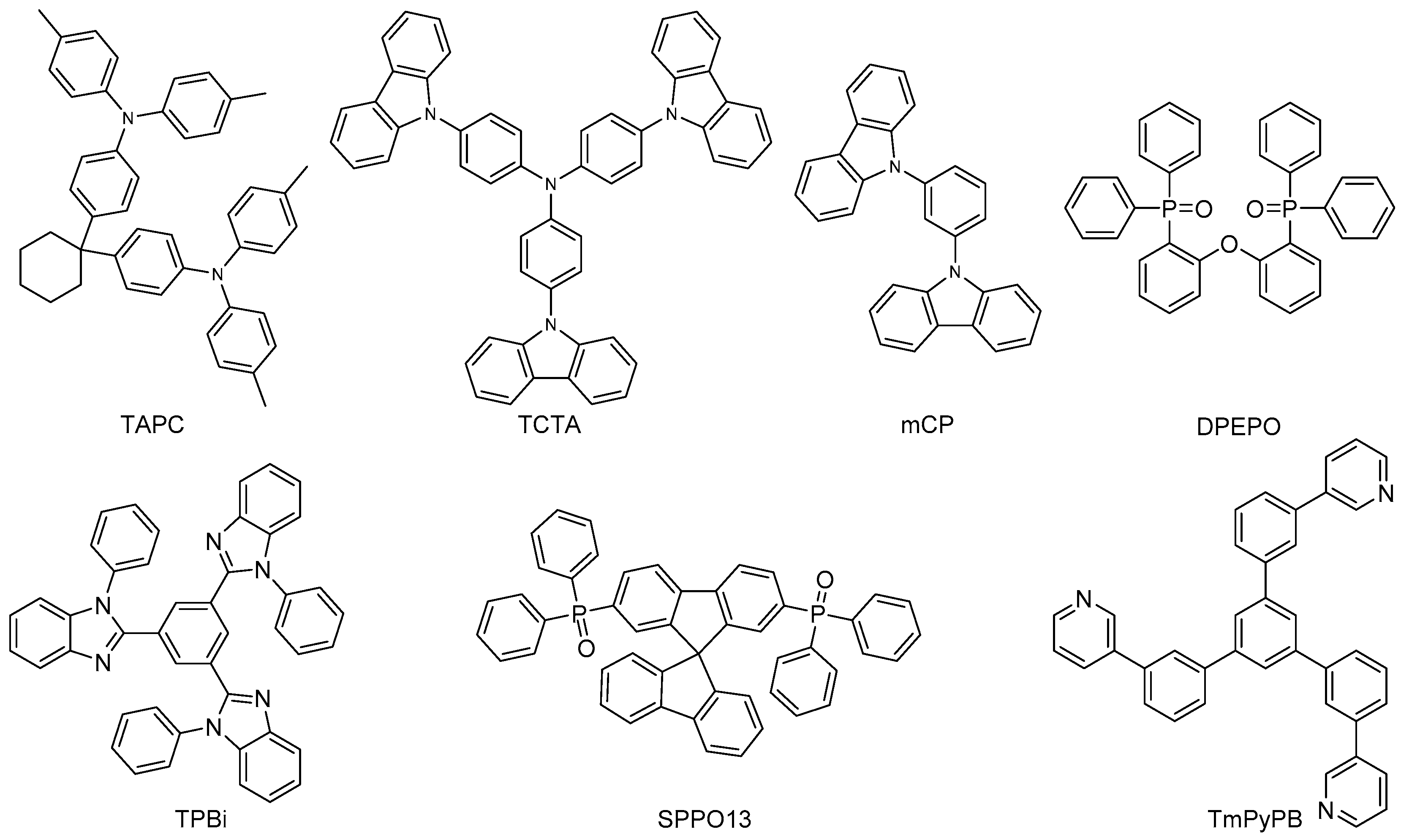
2. Materials and Methods
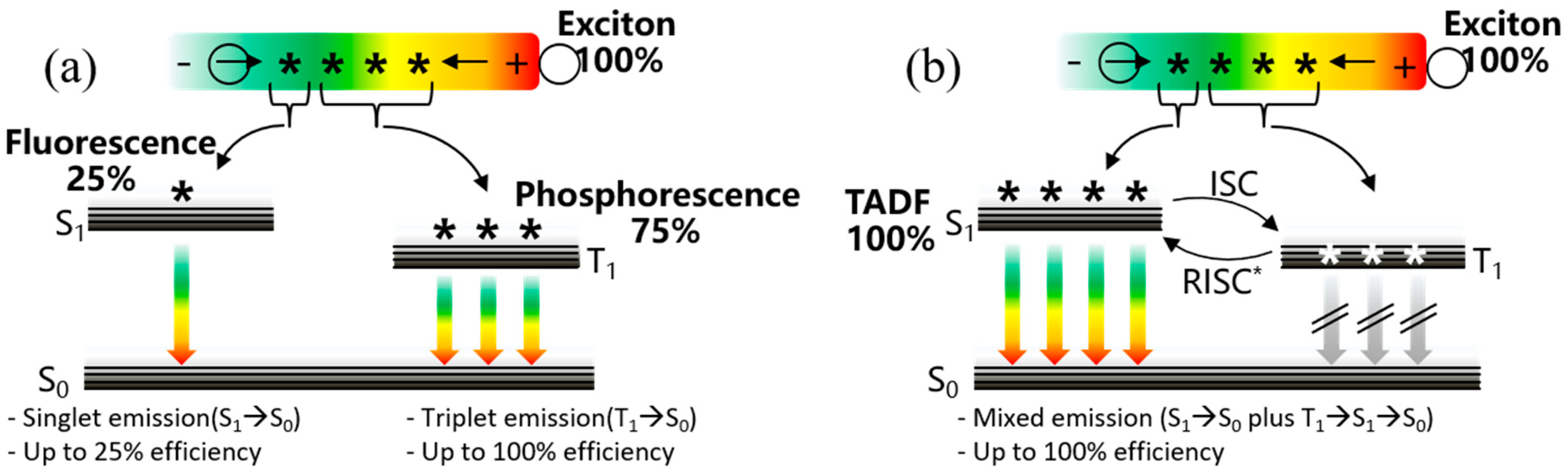
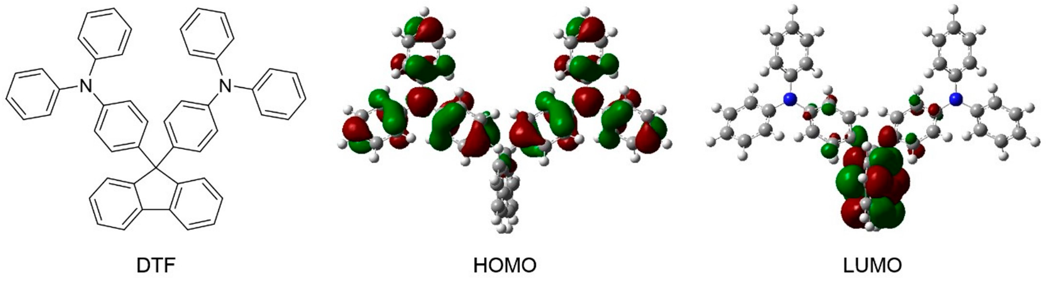
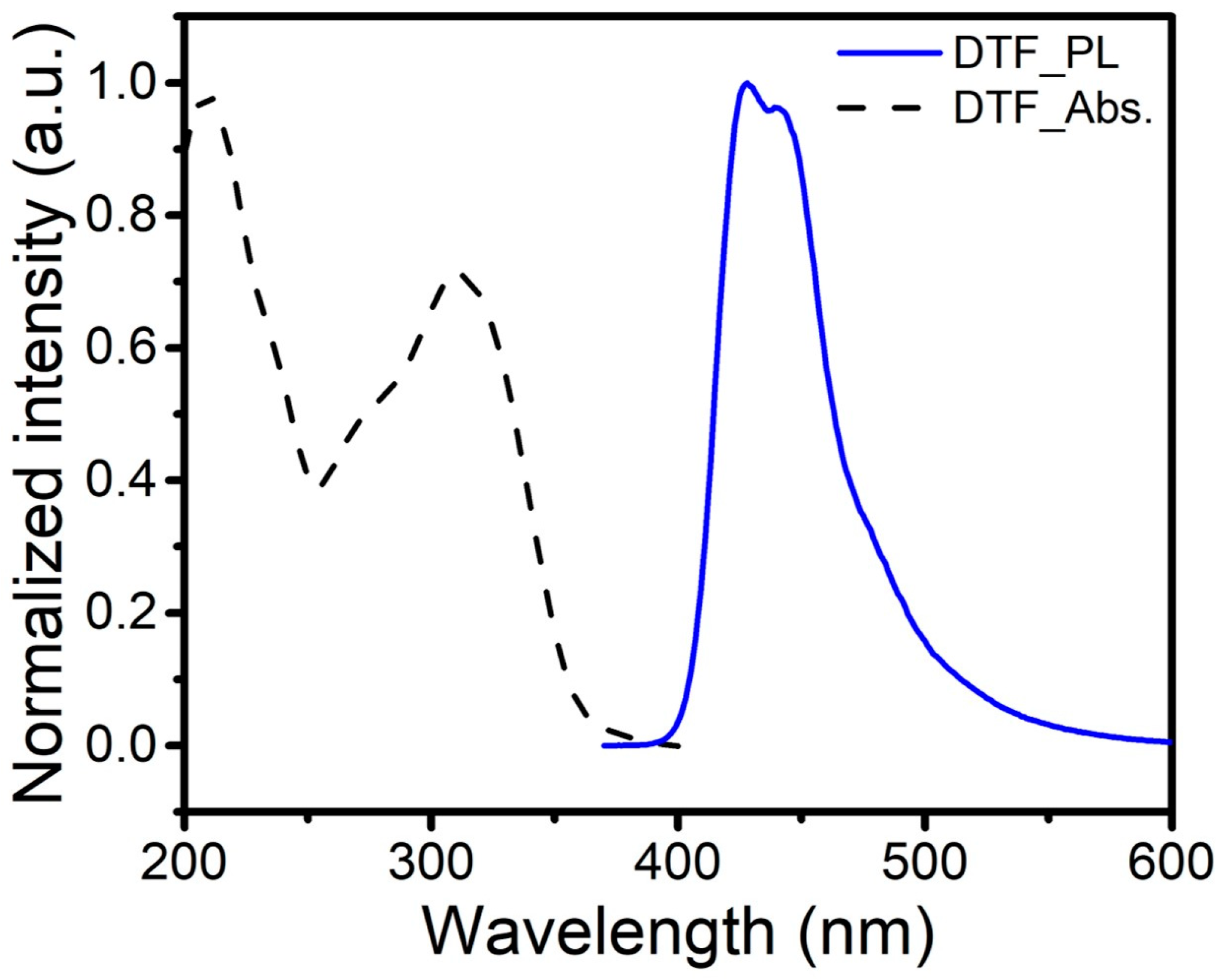
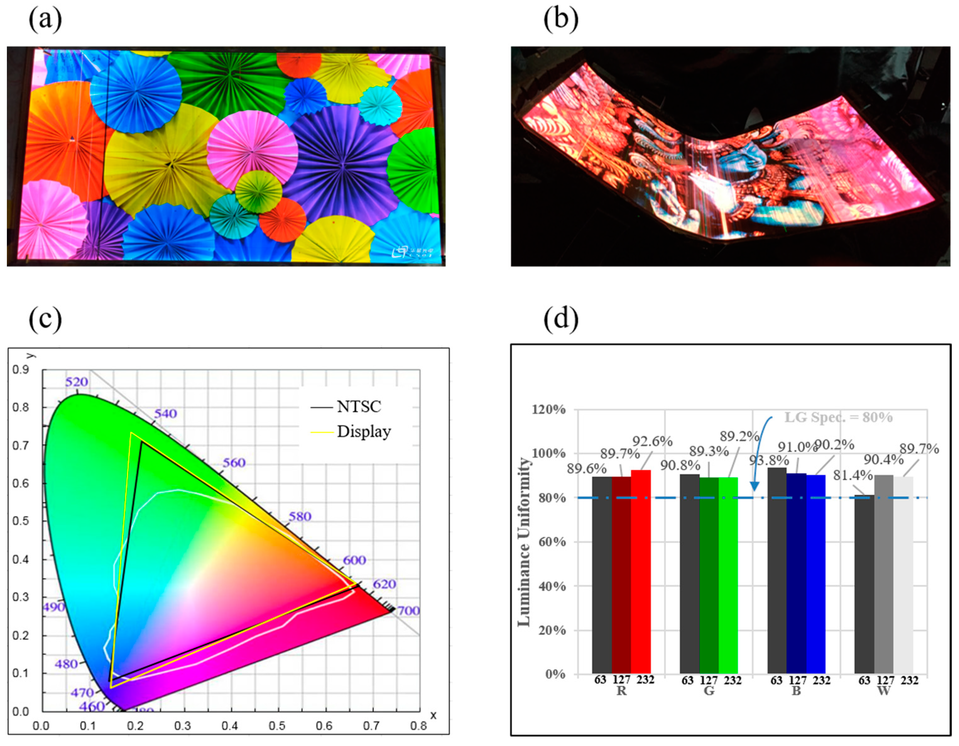
The materials used in this work were supplied by commercial suppliers (Lumtec) without additional purification.
The optical absorption spectrum was measured using Hitachi ultraviolet-visible spectrophotometer U-3010. The fluorescence spectrum was measured using Hitachi fluorescence spectrometer F-4600 [37].
Indium tin oxide (ITO)-coated glass substrates with a thickness of 135 nm and a sheet resistance of 15 Ω sq−1 were successively cleaned with detergent and deionized water. Then, they were dried in an oven at 110 °C for more than 2 h and then treated with ultraviolet ozone for 15 min. The organic layers LiF and aluminum were thermally evaporated at rates of 1.0, 0.1 and 10.0 Å s−1, respectively. The evaporation rate was monitored by a quartz crystal.
The voltage and current were measured by a computer-controlled Keithley 2400 source meter. The luminance characteristics were measured with a Spectrascan PR655 photometer under ambient atmosphere. CE and PE of the devices were calculated using the measured luminance, current, voltage and its lighting area. The EQE of the device was calculated from the current density, luminance, and EL spectrum, assuming a Lambertian distribution [38,39].

3. Results

The DTF is composed of a fluorene core and TPA side groups and is usually used as a hole-transporting material [40]. We noticed that fluorene is a core structure that can emit ultraviolet light and has a high PLQY (0.72) [41]. We think that DTF may be a promising candidate for deep-blue fluorescent materials. Density function theory (DFT) calculations (Gaussian 09 program) are used to study the B3LYP/6-31G (d) basis set. We can see that the TPA plane and fluorene plane are almost perpendicular to each other in Figure 2. This twisted conformation helps to reduce the π-π stacking between molecules. The highest occupied molecular orbital (HOMO) and the lowest unoccupied molecular orbital (LUMO) of DTF are distributed at the electron-rich triphenylamine moiety and the fluorene moiety, respectively [42].
The characteristics of the DTF films characterized under room temperature can be seen in Figure 3. The DTF films exhibit ultraviolet absorption with peaks at 209.0 nm, 279.0 nm, and 311.0 nm. As shown in the PL spectrum, a mixture of two adjacent peaks, 427.0 nm and 450.0 nm, can be evidently observed, respectively. Meanwhile, the FWHM is estimated to be 48 nm. Furthermore, the PLQY of DTF in DCM is measured to be 0.97. The above results indicate that DTF is a promising deep-blue fluorescent emitter.
The detailed deposition process of Device 1 is shown in Figure 4a, as follows: Firstly, a 30 nm thick 4,40-bis [N-(1-naphthyl)-N-phenyl] biphenyl diamine (α-NPD) film was deposited on the ITO template. Secondly, a 20 nm thick 4,4′,4″-tris(N-carbazolyl) triphenylamine (TCTA) layer was fabricated and patterned on the α-NPD layer. Subsequently, a 10 nm thick 9-(4-tert-butylphenyl)-3,6-bis(triphenylsilyl)-9H-carbazole (CzSi) layer and a 20 nm thick bis (2-(diphenylphosphino)phenyl) ether oxide (DPEPO):16 wt% DTF layer were deposited in sequence on the TCTA layer, and then a 30 nm thick 1,3,5-tris(N-phenylbenzimidazol-2-yl)benzene (TPBi) layer and a 0.8 nm thick LiF (0.8 nm) layer were deposited in sequence on the DPEPO layer. Finally, 80 nm thick aluminium (Al) was used as a cathode electrode for the OLED device.
Excitons can be combined well in the DTF films because DPEPO has a high singlet energy level (S1) and triplet energy level (T1). It should be mentioned that the doping concentration of DTF in the emitting layer (EML) is optimized to 16 wt%. Figure 4b shows the electroluminescence (EL) spectra with a different luminance. Device 1 exhibits the same deep-blue emission peaks at 427.0 nm, which is consistent with the PL spectrum. The CIE coordinates of Device 1 are measured to be (0.155, 0.051), demonstrating that the deep-blue OLED device can be fabricated. As shown in the J-V-L plots (Figure 4c), device 1 exhibits a high turn-on voltage (Von = 4.5 V, seen in Table 1), which may be caused by a large injection barrier between DPEPO and TPBi. As depicted in Figure 4d, Device 1 achieves a high EQE (4.5%).
Note that Device 1 exhibits a relatively high Von and low power efficiency (PE = 1.4 lm/W). Therefore, we investigated devices using mCP as the host and TPBi/2,7-bis(diphenylphosphoryl)-9,90-spirobi[fluorene] (SPPO13)/1,3-tri[(3-pyridyl)-phen-3-yl]-benzene (TmPyPB) as the ETL, with the configuration (as shown in Figure 5a) of di-[4-(N,Ndi-tolyl-amino)-phenyl]cyclohexane (TAPC) (40 nm)/TCTA (10 nm)/1,3-bis(carbazole-9-yl)benzene (mCP):24 wt% DTF (20 nm)/ETL (45 nm)/LiF (0.8 nm). The doping concentration of DTF is optimized to 24 wt%. The materials of the ETL layers are TPBi, SPPO13, and TmPyPB for Devices 2-1, 2-2, and 2-3, respectively. Figure 5b shows the EL spectra of Devices 2-1, 2-2, and 2-3 at different luminances. In the normalized EL spectra of Device 1, the intensity of the peak at 427 nm is higher than the peak at 450 nm. However, in Devices 2-1, 2-2 and 2-3, the intensity of the peak at 450 nm is higher than the peak at 427 nm. Therefore, there is a slight red shift of Devices 2-1, 2-2 and 2-3 compared to Device 1. The red shift may be caused by poor exciton confinement in the EML and can be estimated by the CIE coordinate variation [43]. The CIE coordinates of Devices 2-1, 2-2 and 2-3 are measured to be (0.160, 0.064), (0.151, 0.062) and (0.151, 0.056). The emissions of Devices 2-1, 2-2, 2-3 are slightly red-shifted compared with Device 1. The J-V-L plots are shown in Figure 5c. Devices 2-1, 2-2, and 2-3 exhibit a lower Von of 3.2 V, 3.1 V and 3.1 V (shown in Table 1). The lower Von may be caused by a lowered injection barrier. Moreover, as shown in Figure 5d, Devices 2-1, 2-2 and 2-3 exhibit a lower external EQE of 2.7%, 1.2% and 1.7%, respectively.
In contrast to the Device 1, Devices 2-1, 2-2, and 2-3 exhibit a lower Von and lower EQE, which may be caused by hole leakage from EML to ETL. DPEPO with a larger steric hindrance, higher energy gap and higher excited state energy levels possess a better capacity for hole blocking and exciton confinement in the deep-blue device. Therefore, we use DPEPO as a hole-blocking layer and investigate Device 3 with the configuration shown in Figure 6a: TAPC (40 nm)/TCTA (10 nm)/mCP:24 wt% DTF (20 nm)/DPEPO (5 nm)/TmPyPB (45 nm)/LiF (0.8 nm). The thickness of DPEPO is optimized to 5 nm. The EL spectra of Device 3 are depicted in Figure 6b, indicating stable deep-blue emission peaks at 427.0 nm in this device with the CIE coordinates of (0.155, 0.055). The J-V-L plots are shown in Figure 6c. Device 3 exhibits a Von of 3.3 V (shown in Table 1). Most importantly, Device 3 exhibits a high EQE of 5.0% in Figure 6d. It is challenging for the CIE y of TADF blue emitters to reach a deeper region (CIE y < 0.06) [44]. Normally, most reported OLEDs with CIE y < 0.06 were achieved by traditional fluorescent deep-blue emitters. Here, deep-blue fluorescent OLEDs with a high EQE of 5.0% (reaching the theoretical limit) were reported.
An AMOLED display was used to test the OLED device (Device 3), which was prepared on a flexible polyimide (PI) substrate. As shown in Figure 7a, the display features an external compensation sub-pixel circuit composed of three thin film transistors (TFT, T1–T3) and one storage capacitance (Cst) to provide a stable driving circuit for the OLED device. The cathode electrode of the OLED device is connected to the low-level power source (VSS = 0 V), while the anode electrode is connected to the source electrode of the driving TFT (T1). When the scan signal (WR) is selected, VData is transported to the gate electrode of T1, allowing the brightness of the OLED to be adjusted via the driving current generated by T1. The circuit design ensures the reliable performance of the OLED device.
Figure 7b illustrates the sub-pixel arrangement in each pixel of the top-emitting flexible AMOLED display. Each pixel is composed of three sub-pixels (Red/Green/Blue). The areas of OLED are 4664 μm2 for R sub-pixel, 5088 μm2 for G sub-pixel and 5862 μm2 for B sub-pixel, respectively. Meanwhile, the pixel size is 29,756.25 μm2. Therefore, the average aperture ratio (the proportion of OLED area in the pixel) is 52.5%. Figure 7c shows the pixel expanding horizontally and vertically in two dimensions. The scan signals (WR1~WR2160, RD1~RD2160) are generated by the gate driver circuits. The data lines are connected to the external source IC.
Figure 7d presents the schematic diagram of the 31-inch AMOLED display on the plastic substrate. The process starts by coating the PI substrate, with a thickness of 10 μm, on the carrier glass using a slot-die coater. Next, a stack of SiO2/Si3N4/SiO2 films is deposited on the PI to serve as a template layer for the TFT arrays. The indium-gallium-zinc oxide (IGZO)-TFTs are then fabricated on the inorganic SiO2/Si3N4/SiO2 films, followed by the deposition of the OLED films on the TFT arrays in an AMOLED manufacturing factory. Finally, the laser lift-off process is used to peel off the PI from the carrier glass, as shown in Figure 7d. This fabrication process ensures the reliability and flexibility of the AMOLED display. The mechanical properties of the prepared flexible structure can be seen in our previous study [3].
Our team has performed lighting tests on the fabricated OLED device, and as shown in Figure 8a, all pixels (2160 × 3840) light up successfully, demonstrating the functionality of the OLED devices. Additionally, even after the laser lift-off process, the display still works well, as shown in Figure 8b. In our previous study [3], the flexible display was continuously operated for 500 h. Colorimetric measurements were taken using the CIE at (0.72, 0.28), completely covering the BT.2020 color gamut (the black line in Figure 8c). The luminance uniformity of the flexible display was systematically studied using the following equation:
P i = ( 1 | L i L c e n t e r L c e n t e r | )
where Lcenter is the luminance at the center of the display, Li is the luminance at the other place in the display, and Pi is the luminance uniformity. The luminance uniformity of low grays (63 gray), medium grays (127 gray) and high grays (232 gray) in different pictures (R/G/B/W) can be seen in Figure 8d. It should be mentioned that all the gray scales can reach the LG’s brightness uniformity spec (80%), indicating that the OLED devices and the displays fabricated in our laboratory can reach industrialization requirements.

4. Conclusions

In conclusion, we have found that traditional hole-transporting material is a promising deep-blue fluorescent emitter. (1) A mixture of two adjacent peaks at 427.0 nm and 450.0 nm can be evidently observed in DTF films. Furthermore, the PLQY of DTF in DCM is measured to be 0.97; (2) A device utilizing DTF as an emitter exhibits deep-blue emission peaks at 427.0 nm, which is consistent with the PL spectrum. The device exhibits CIE coordinates of (0.155, 0.051), a Von of 4.5 V, and an EQE of 4.5%; (3) By optimizing the device structure, a Von of 3.3 V and EQE of 5.0% can be obtained; (4) Finally, confirming the OLED device described above (Device 3), the flexible AMOLED display exhibits a high image quality, demonstrating the high performance of the OLED devices.

Author Contributions

Y.X., Q.N., X.H. and B.W. contributed to the device design, data analysis, and writing. The material preparation and data collection were performed by Y.C., Y.Z. and L.X. All authors have read and agreed to the published version of the manuscript.

Funding

We gratefully acknowledge funding from the Basic and Applied Basic Research Funding of Guangdong (No. 2020A1515110551), Provincial Education Department of Guangdong (No. 2021KTSCX277), Shenzhen Science and Technology Program (No. RCBS20210609103648040), The Second Batch of High-level Professional Cluster in Majors for Vocational Colleges in Guangdong Province (No. GSPZYQ2021079), Provincial High Vocational Education Teaching Reform Research and Practice Project (GDJG2021422). Key funded projects of special funds for scientific and technological innovation strategy of Guangdong Province (pdjh2022a0973, pdjh2022001, pdjh2023a0967), Shenzhen Science and Technology Program under grant (20220814133504001), Post-doctoral Later-stage Foundation Project of Shenzhen Polytechnic under grant (6021271013K), and the Founding of Shenzhen polytechnic (Nos. 6021310007K, 6022312061K, 6022310034K, 6021271011K, 6021230059K, 6021210078K, LHRC20220402, 1019-8122310001C0, 6022310030K) for this work.

Data Availability Statement

All data generated or analyzed during this study are included in this article.

Conflicts of Interest

The authors declare that they have no known competing financial interests or personal relationships that could have appeared to influence the work reported in this paper.

References

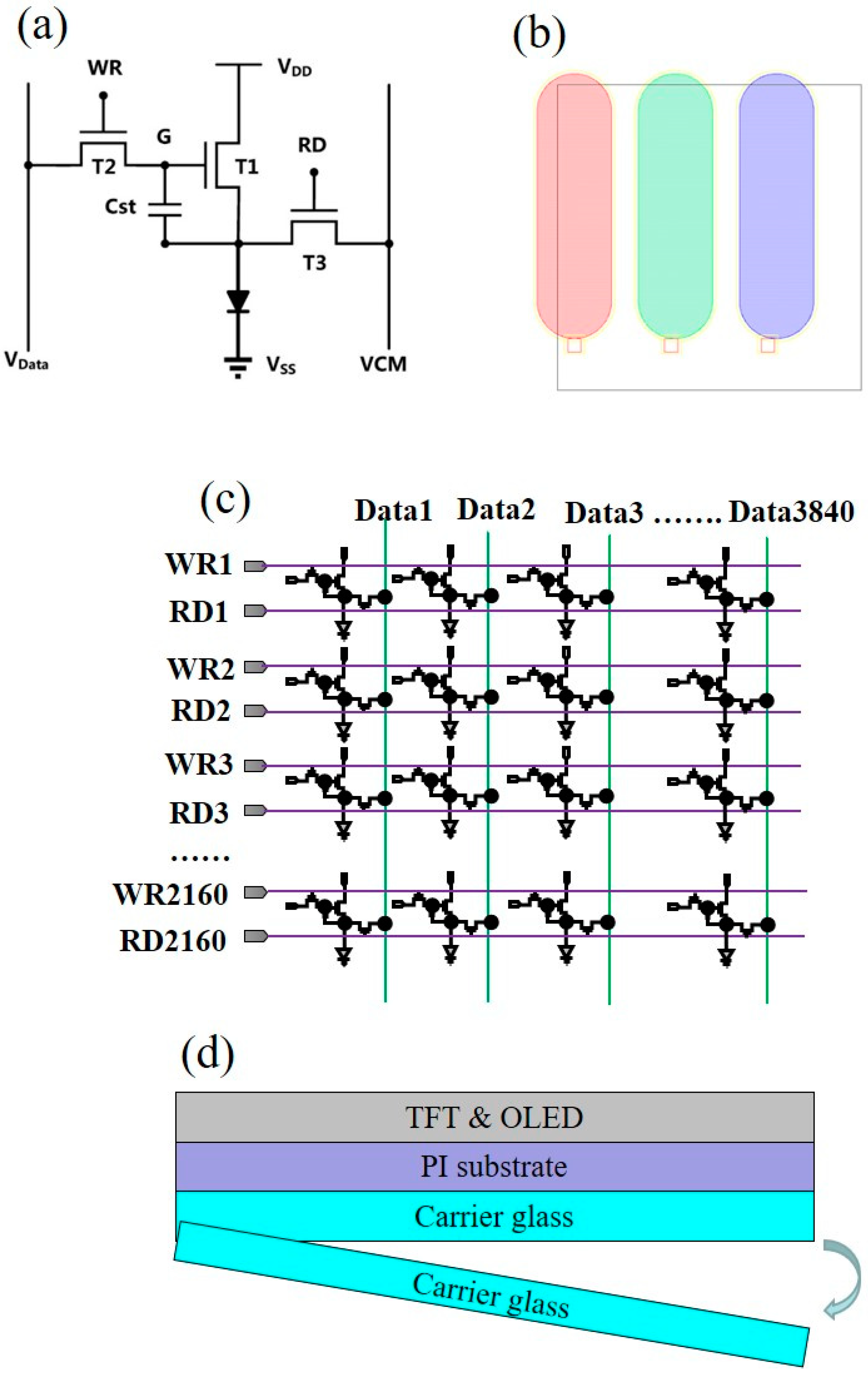
  1. Song, R.; Wu, Y.; Lin, C.; Liu, K.; Qing, Z.; Li, Y.; Xue, Y. High-Speed Shift Register with Dual-Gated Thin-Film Transistors for a 31-Inch 4K AMOLED Display. Micromachines 2022, 13, 1696. [Google Scholar] [CrossRef]
  2. Yang, X.; Xu, X.; Zhou, G. Recent advances of the emitters for high performance deep-blue organic light-emitting diodes. J. Mater. Chem. C 2015, 3, 913–944. [Google Scholar] [CrossRef]
  3. Xue, Y.; Wang, L.; Zhang, Y.; Liang, G.; Chu, J.; Han, B.; Cao, W.; Liao, C.; Zhang, S. 31-inch 4K flexible display employing gate driver with metal oxide thin-film transistors. IEEE Electron Device Lett. 2021, 42, 188–191. [Google Scholar] [CrossRef]
  4. Tang, X.; Bai, Q.; Peng, Q.; Gao, Y.; Li, J.; Liu, Y.; Yao, L.; Lu, P.; Yang, B.; Ma, Y. Efficient Deep Blue Electroluminescence with an External Quantum Efficiency of 6.8% and CIEy < 0.08 Based on a Phenanthroimidazole-Sulfone Hybrid Donor-Acceptor Molecule. Chem. Mater. 2015, 27, 151006104612009. [Google Scholar]
  5. Lee, M.T.; Liao, C.H.; Tsai, C.H.; Chen, C.H. Deep-blue doped organic light-emitting devices. Adv. Mater. 2005, 17, 2493–2497. [Google Scholar] [CrossRef]
  6. Zhao, J.; Liu, B.; Wang, Z.; Tong, Q.; Du, X.; Zheng, C.; Lin, H.; Tao, S.; Zhang, X. EQE climbing over 6% at high brightness of 14350 cd/m2 in deep-blue OLEDs based on hybridized local and charge-transfer fluorescence. ACS Appl. Mater. Interfaces 2018, 10, 9629–9637. [Google Scholar] [CrossRef]
  7. Kim, S.K.; Yang, B.; Ma, Y.; Lee, J.H.; Park, J.W. Exceedingly efficient deep-blue electroluminescence from new anthracenes obtained using rational molecular design. J. Mater. Chem. 2008, 18, 3376–3384. [Google Scholar] [CrossRef]
  8. Kim, M.; Jeon, S.K.; Hwang, S.H.; Lee, S.S.; Yu, E.; Lee, J.Y. Correlation of molecular structure with photophysical properties and device performances of thermally activated delayed fluorescent emitters. J. Phys. Chem. C 2016, 120, 2485–2493. [Google Scholar] [CrossRef]
  9. Chen, S.; Tan, G.; Wong, W.Y.; Kwok, H.S. White Organic Light-Emitting Diodes with Evenly Separated Red, Green, and Blue Colors for Efficiency/Color-Rendition Trade-Off Optimization. Adv. Funct. Mater. 2011, 21, 3785–3793. [Google Scholar] [CrossRef]
  10. Yang, Z.; Mao, Z.; Xie, Z.; Zhang, Y.; Liu, S.; Zhao, J.; Xu, J.; Chi, Z.; Aldred, M.P. Recent advances in organic thermally activated delayed fluorescence materials. Chem. Soc. Rev. 2017, 46, 915–1016. [Google Scholar] [CrossRef]
  11. Wu, T.L.; Huang, M.J.; Lin, C.C.; Huang, P.Y.; Chou, T.Y.; Chen-Cheng, R.W.; Lin, H.W.; Liu, R.S.; Cheng, C.H. Diboron compound-based organic light-emitting diodes with high efficiency and reduced efficiency roll-off. Nat. Photonics 2018, 12, 235–240. [Google Scholar] [CrossRef]
  12. Sarma, M.; Wong, K.T. An intermolecular charge-transfer approach for TADF. ACS Appl. Mater. Interfaces 2018, 10, 19279–19304. [Google Scholar] [CrossRef] [PubMed]
  13. Li, M.; Li, S.H.; Zhang, D.; Cai, M.; Duan, L.; Fung, M.K.; Chen, C.F. Stable enantiomers displaying thermally activated delayed fluorescence: Efficient OLEDs with circularly polarized electroluminescence. Angew. Chem. Int. Ed. 2018, 57, 2889–2893. [Google Scholar] [CrossRef]
  14. Lee, J.H.; Chen, C.H.; Lee, P.H.; Lin, H.Y.; Leung, M.K.; Chiu, T.L.; Lin, C.F. Blue organic light-emitting diodes: Current status, challenges, and future outlook. J. Mater. Chem. C 2019, 7, 5874–5888. [Google Scholar] [CrossRef]
  15. Huang, T.; Jiang, W.; Duan, L. Recent progress in solution processable TADF materials for organic light-emitting diodes. J. Mater. Chem. C 2018, 6, 5577–5596. [Google Scholar] [CrossRef]
  16. Chen, X.-K.; Kim, D.; Bredas, J.-L. Thermally activated delayed fluorescence (TADF) path toward efficient electroluminescence in purely organic materials: Molecular level insight. Acc. Chem. Res. 2018, 51, 2215–2224. [Google Scholar] [CrossRef]
  17. Yook, K.S.; Lee, J.Y. Organic materials for deep blue phosphorescent organic light-emitting diodes. Adv. Mater. 2012, 24, 3169–3190. [Google Scholar] [CrossRef] [PubMed]
  18. Kim, R.; Lee, S.; Kim, K.H.; Lee, Y.J.; Kwon, S.K.; Kim, J.J.; Kim, Y.H. Extremely deep blue and highly efficient non-doped organic light emitting diodes using an asymmetric anthracene derivative with a xylene unit. Chem. Commun. 2013, 49, 4664–4666. [Google Scholar] [CrossRef]
  19. Li, Y.; Li, X.L.; Cai, X.; Chen, D.; Liu, X.; Xie, G.; Wang, Z.; Wu, Y.C.; Lo, C.C.; Lien, A.; et al. Deep blue fluorophores incorporating sulfone-locked triphenylamine: The key for highly efficient fluorescence–phosphorescence hybrid white OLEDs with simplified structure. J. Mater. Chem. C 2015, 3, 6986–6996. [Google Scholar] [CrossRef]
  20. Qin, W.; Yang, Z.; Jiang, Y.; Larn, J.W.Y.; Liang, G.; Kwok, H.S.; Tang, B.Z. Construction of efficient deep blue aggregation-induced emission luminogen from triphenylethene for nondoped organic light-emitting diodes. Chem. Mater. 2015, 27, 3892–3901. [Google Scholar] [CrossRef]
  21. Zhang, Z.; Wu, Y.S.; Tang, K.C.; Chen, C.L.; Ho, J.W.; Su, J.; Tian, H.; Chou, P.T. Excited-state conformational/electronic responses of saddle-shaped N,N′-disubstituted-dihydrodibenzo[a,c]phenazines: Wide-tuning emission from red to deep blue and white light combination. J. Am. Chem. Soc. 2015, 137, 8509–8520. [Google Scholar] [CrossRef]
  22. Lee, J.; Chen, H.F.; Batagoda, T.; Coburn, C.; Djurovich, P.I.; Thompson, M.E.; Forrest, S.R. Deep blue phosphorescent organic light-emitting diodes with very high brightness and efficiency. Nat. Mater. 2016, 15, 92–98. [Google Scholar] [CrossRef] [PubMed]
  23. Shan, T.; Liu, Y.; Tang, X.; Bai, Q.; Gao, Y.; Gao, Z.; Li, J.; Deng, J.; Yang, B.; Lu, P.; et al. Highly efficient deep blue organic light-emitting diodes based on imidazole: Significantly enhanced performance by effective energy transfer with negligible efficiency roll-off. ACS Appl. Mater. Interfaces 2016, 8, 28771–28779. [Google Scholar] [CrossRef]
  24. Kondo, Y.; Yoshiura, K.; Kitera, S.; Nishi, H.; Oda, S.; Gotoh, H.; Sasada, Y.; Yanai, M.; Hatakeyama, T. Narrowband deep-blue organic light-emitting diode featuring an organoboron-based emitter. Nat. Photonics 2019, 13, 678–682. [Google Scholar] [CrossRef]
  25. Ahn, D.H.; Kim, S.W.; Lee, H.; Ko, I.J.; Karthik, D.; Lee, J.Y.; Kwon, J.H. Highly efficient blue thermally activated delayed fluorescence emitters based on symmetrical and rigid oxygen-bridged boron acceptors. Nat. Photonics 2019, 13, 540–546. [Google Scholar] [CrossRef]
  26. Lee, H.L.; Chung, W.J.; Lee, J.Y. Narrowband and Pure Violet Organic Emitter with a Full Width at Half Maximum of 14 nm and y Color Coordinate of Below 0.02. Small 2020, 16, 1907569. [Google Scholar] [CrossRef] [PubMed]
  27. Gao, Z.; Liu, Y.; Wang, Z.; Shen, F.; Liu, H.; Sun, G.; Yao, L.; Lv, Y.; Lu, P.; Ma, Y. High-efficiency violet-light-emitting materials based on phenanthro[9,10-d]imidazole. Chem. Eur. J. 2013, 19, 2602–2605. [Google Scholar] [CrossRef] [PubMed]
  28. Poriel, C.; Berthelot, J.R. Blue Single-Layer Organic Light-Emitting Diodes Using Fluorescent Materials: A Molecular Design View Point. Adv. Funct. Mater. 2020, 30, 1910040. [Google Scholar] [CrossRef]
  29. Dayneko, S.V.; Cieplechowicz, E.; Bhojgude, S.S.; Van Humbeck, J.F.; Pahlevani, M.; Welch, G.C. Improved performance of solution processed OLEDs using N-annulated perylene diimide emitters with bulky side-chains. Mater. Adv. 2021, 2, 933–936. [Google Scholar] [CrossRef]
  30. Chettri, B.; Patra, P.K.; Verma, S.; Rao, B.K.; Verma, M.L.; Thakur, V.; Kumar, N.; Hieu, N.N.; Rai, D.P. Induced magnetic states upon electron–hole injection at B and N sites of hexagonal boron nitride bilayer: A density functional theory study. Int. J. Quantum Chem. 2021, 121, e26680. [Google Scholar] [CrossRef]
  31. Cui, D.; Wang, S.; Li, S.; Liu, Y.; Gao, X.; Wang, W.; Dong, X. Improving the performance of OLEDs by controlling the molecular orientation in charge carrier transport layers. Opt. Express 2021, 29, 16845–16856. [Google Scholar] [CrossRef] [PubMed]
  32. Tang, M.C.; Lee, C.H.; Ng, M.; Wong, Y.C.; Chan, M.Y.; Yam, V.W.W. Highly Emissive Fused Heterocyclic Alkynylgold (III) Complexes for Multiple Color Emission Spanning from Green to Red for Solution-Processable Organic Light-Emitting Devices. Angew. Chem. Int. Ed. 2018, 57, 5463–5466. [Google Scholar] [CrossRef] [PubMed]
  33. Teng, J.M.; Wang, Y.F.; Chen, C.F. Recent progress of narrowband TADF emitters and their applications in OLEDs. J. Mater. Chem. C 2020, 8, 11340–11353. [Google Scholar] [CrossRef]
  34. Kim, S.; Kim, B.; Lee, J.; Shin, H.; Park, Y.-I.; Park, J. Design of fluorescent blue light-emitting materials based on analyses of chemical structures and their effects. Mater. Sci. Eng. R Rep. 2016, 99, 1–22. [Google Scholar] [CrossRef]
  35. Wan, Z.; Zhang, Y.; Yang, J.; Xia, J.; Lin, F.; Yao, X.; Luo, J.; Jia, C. Simple hybrid dithiafulvenes-triphenylamine systems as dopant-free hole-transporting materials for efficient perovskite solar cells. J. Energy Chem. 2022, 68, 293–299. [Google Scholar] [CrossRef]
  36. Hai, J.; Wu, H.; Yin, X.; Song, J.; Hu, L.; Jin, Y.; Li, L.; Su, Z.; Xu, Z.; Wang, H.; et al. Dopant-Free Hole Transport Materials Based on a Large Conjugated Electron-Deficient Core for Efficient Perovskite Solar Cells. Adv. Funct. Mater. 2021, 31, 2105458. [Google Scholar] [CrossRef]
  37. Xie, G.; Luo, J.; Huang, M.; Chen, T.; Wu, K.; Gong, S.; Yang, C. Inheriting the characteristics of TADF small molecule by side-chain engineering strategy to enable bluish-green polymers with high PLQYs up to 74% and external quantum efficiency over 16% in light-emitting diodes. Adv. Mater. 2017, 29, 1604223. [Google Scholar] [CrossRef]
  38. Udagawa, K.; Sasabe, H.; Igarashi, F.; Kido, J. Simultaneous Realization of High EQE of 30%, Low Drive Voltage, and Low Efficiency Roll-Off at High Brightness in Blue Phosphorescent OLEDs. Adv. Opt. Mater. 2016, 4, 86–90. [Google Scholar] [CrossRef]
  39. Yan, C.C.; Wang, X.D.; Liao, L.S. Thermally activated delayed fluorescent gain materials: Harvesting triplet excitons for lasing. Adv. Sci. 2022, 9, 2200525. [Google Scholar] [CrossRef]
  40. Huang, F.; Cheng, Y.J.; Zhang, Y.; Liu, M.S.; Jen, A.K.Y. Crosslinkable hole-transporting materials for solution processed polymer light-emitting diodes. J. Mater. Chem. 2008, 18, 4495–4509. [Google Scholar] [CrossRef]
  41. Kang, S.; Jung, H.; Lee, H.; Park, S.; Kim, J.; Park, J. Highly efficient dual-core derivatives with EQEs as high as 8.38% at high brightness for OLED blue emitters. J. Mater. Chem. C 2019, 7, 14709–14716. [Google Scholar] [CrossRef]
  42. Halls, M.D.; Schlegel, H.B. Molecular orbital study of the first excited state of the OLED material tris (8-hydroxyquinoline) aluminum (III). Chem. Mater. 2001, 13, 2632–2640. [Google Scholar] [CrossRef]
  43. Wu, C.L.; Chang, C.H.; Chang, Y.T.; Chen, C.T.; Chen, C.T.; Su, C.J. High efficiency non-dopant blue organic light-emitting diodes based on anthracene-based fluorophores with molecular design of charge transport and red-shifted emission proof. J. Mater. Chem. C 2014, 2, 7188–7200. [Google Scholar] [CrossRef]
  44. Aksoy, E.; Danos, A.; Varlikli, C.; Monkman, A.P. Navigating CIE space for efficient TADF downconversion WOLEDs. Dyes Pigments 2020, 183, 108707. [Google Scholar] [CrossRef]
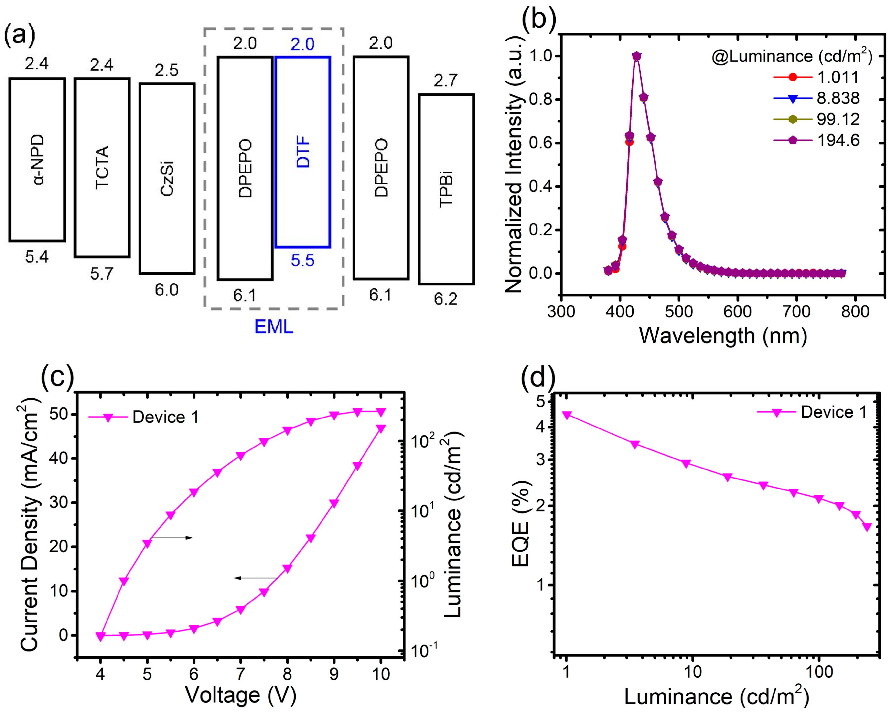
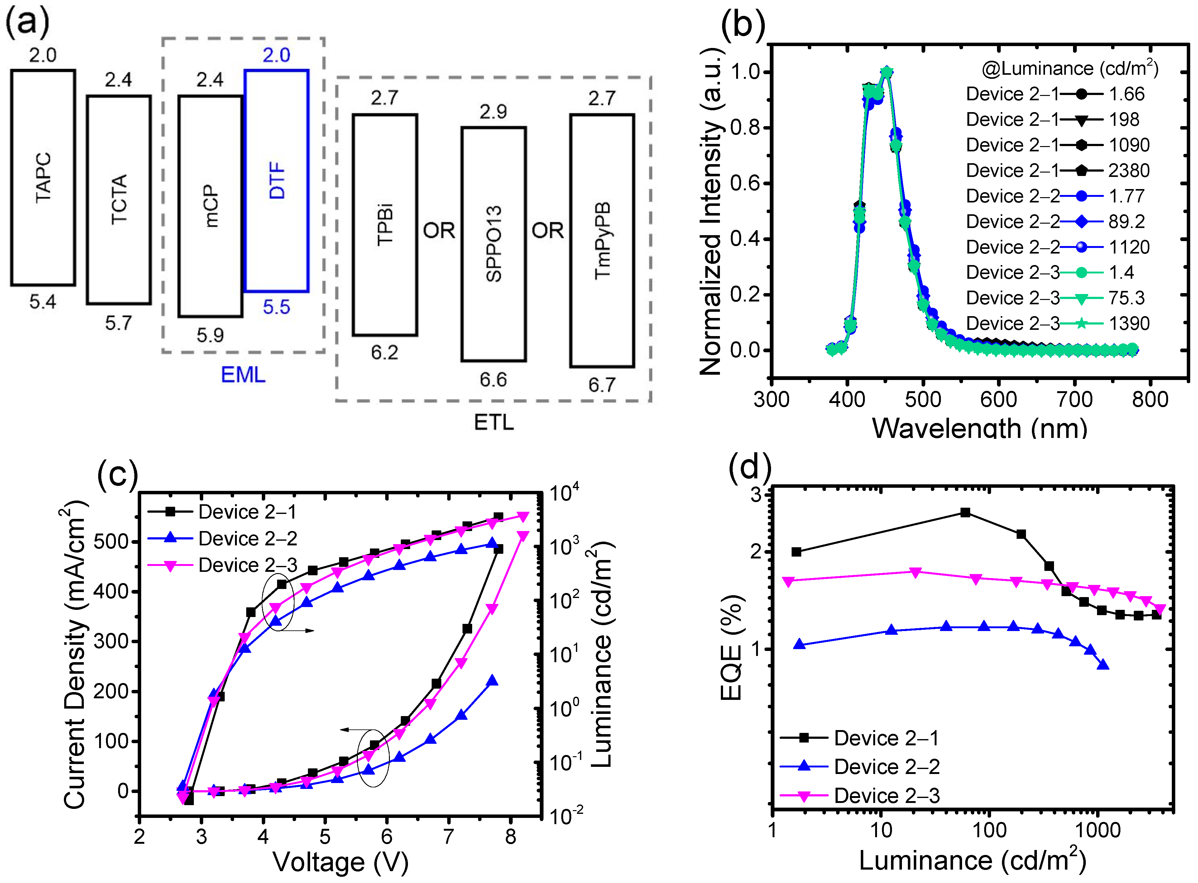
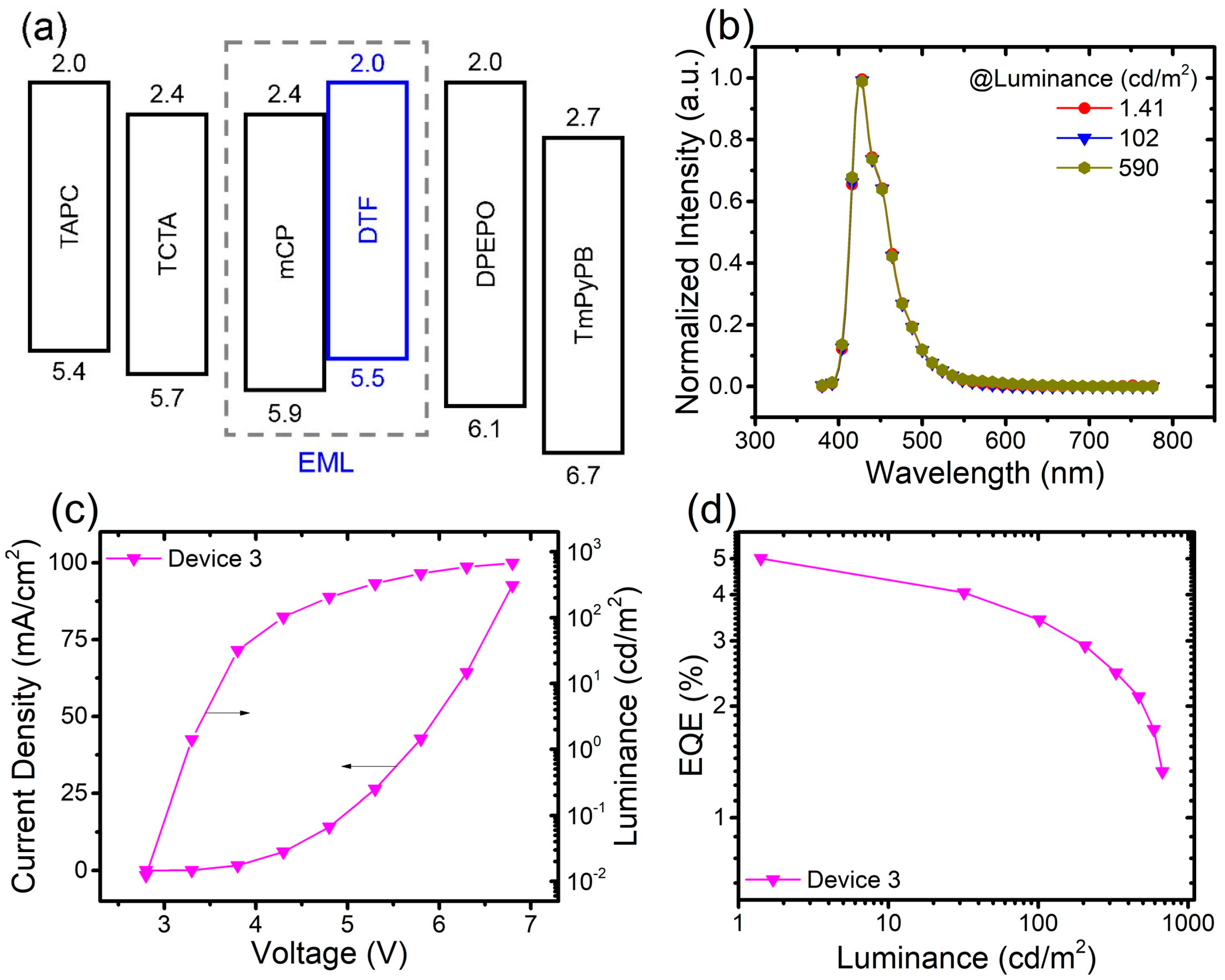
Figure 1. Energy diagram of (a) phosphorescent emitter and (b) TADF emitter.
Crystals 13 00687 g001
Figure 2. The calculated HOMO and LUMO distributions of DTF and molecular structure of materials used in devices.
Crystals 13 00687 g002aCrystals 13 00687 g002b
Figure 3. The ultraviolet absorption and PL spectra of DTF films.
Crystals 13 00687 g003
Figure 4. Device 1: (a) structure and HOMO, LUMO energy levels (in eV); (b) EL spectra; (c) current density-voltage-luminance (J-V-L) plots; and (d) EQE curve.
Crystals 13 00687 g004
Figure 5. Devices 2-1, 2-2 and 2-3: (a) structure and HOMO, LUMO energy levels (in eV); (b) EL spectra at different luminance; (c) J-V-L plots; and (d) EQE curves.
Crystals 13 00687 g005
Figure 6. Device 3: (a) Structure and HOMO, LUMO energy levels (in eV); (b) EL spectra with different luminance; (c) J-V-L plots; and (d) EQE curve.
Crystals 13 00687 g006
Figure 7. The 31-inch 4K AMOLED flexible display. (a) The circuit design of each sub-pixel in the display; (b) the sub-pixel arrangement in each pixel; (c) the TFT array diagram of 4K AMOLED display; and (d) the schematic diagram of thin films on the backplane.
Crystals 13 00687 g007
Figure 8. The image of 31-inch 4K AMOLED display on (a) PI/glass template; (b) PI template; (c) CIE color coordinate of the AMOLED display; (d) the brightness difference over the display.
Crystals 13 00687 g008
Table 1. The EL performance summary of the prepared devices in this work.
DeviceVon
[V]
CEMax
[cd/A]
PEMax
[lm/W]
EQEMax
[%]
Peak
[nm]
LMAX
[cd/m2]
CIE
14.52.01.44.5427266.2(0.155, 0.051)
2-13.21.41.22.7427/4503500.0(0.160, 0.064)
2-23.10.70.71.2427/4501120.0(0.151, 0.062)
2-33.10.90.81.7427/4503750.0(0.151, 0.056)
33.32.52.35.0427674.0(0.155, 0.055)
Von: The driving voltage at the luminance of 1 cd/m2; CEMax: The maximum CE; PEMax: The maximum PE; EQEMax: The maximum EQE; Peak: The peak wavelength of EL spectra; LMax: The maximum luminance; CIE: Commission Internationale de L’Eclairage.
Disclaimer/Publisher’s Note: The statements, opinions and data contained in all publications are solely those of the individual author(s) and contributor(s) and not of MDPI and/or the editor(s). MDPI and/or the editor(s) disclaim responsibility for any injury to people or property resulting from any ideas, methods, instructions or products referred to in the content.

