Article

Preparation of HfNbTiTaZr Thin Films by Ionized Jet Deposition Method

Faculty of Nuclear Sciences and Physical Engineering, Czech Technical University in Prague, Břehová 7, 115 19 Prague, Czech Republic
*
Author to whom correspondence should be addressed.
Crystals 2023, 13(4), 580; https://doi.org/10.3390/cryst13040580
Submission received: 6 March 2023 / Revised: 20 March 2023 / Accepted: 23 March 2023 / Published: 28 March 2023

Abstract

:
The ionized jet deposition (IJD) method is applied to the preparation of thin films composed of refractory HfNbTiTaZr high-entropy alloy (HEA). Due to its stoichiometric reliability, the IJD method provides a flexible tool for deposition of complex multi-element materials, such as HEAs. Scanning electron microscopy, energy-dispersion spectroscopy, confocal microscopy, and X-ray diffraction methods are used to characterize the influence of the applied accelerating voltage of the IJD deposition head ranging from 16 to 22 kV on the resulting morphology, chemical composition, thickness, crystalline structure, and phase composition of the layers prepared as 10 mm-wide strips on a single stainless-steel substrate. With a low accelerating voltage applied, the best surface homogeneity is obtained. Transfer coefficient values characterizing the elemental transport between the bulk target and the grown layer are evaluated for each constituting element and applied voltage. With the IJD accelerating voltage approaching 22 kV, the coefficients converge upon the values proportional to the atomic number of the element. Such voltage dependence of the IJD elemental transport might be used as a suitable tool for fine-tuning the elemental composition of layers grown from a single deposition target.

1. Introduction

Studies of a high-entropy alloy (HEA) with the composition HfNbTiTaZr began with the works of Senkov et al., dealing with the preparation of bulk samples of the alloy and analysis of their microstructure and mechanical properties at room as well as elevated temperatures [1,2]. Later interest in the study of this alloy has been stimulated by its good refractory properties and biocompatibility, making it promising, e.g., for high temperature and medical applications [3]. Another area in which this alloy is currently being tested for possible application is hydrogen storage devices, where they could be an economically viable alternative to expensive systems based on hydrates of lanthanides, yttrium, and rare earth metals. For such purposes, a fine-grained microstructure with a high internal surface formed by grain boundaries and opened volume defects is advantageous [4,5].
HfNbTiTaZr HEA shows a better workability than other refractory HEAs of different composition (e.g., MoNbTaVW or MoNbTaW [6,7]) and medium-entropy alloys from the same HfNbTiTaZr system [8]. As reported by Zherebtsov et al., the alloy can be processed by a three-stage cold rolling up to the thickness strain 80%, with the microhardness gradually increasing, and the final microstructure consisting of sheer bands with fine lamellar internal substructure [9]. Changes of the HfNbTiTaZr HEA microstructure associated with microhardness growth were also observed under the influence of annealing at temperatures above 600 °C [10].
The possible range of practical applicability of the alloy can be further promoted by its preparation and utilization in the form of thin coatings prepared on already properly shaped functional parts by a suitable thin-film deposition method. Such an approach provides a convenient way of overcoming some of the limitations of traditional manufacturing practices [11]. Several studies have been recently published dealing with thin layers prepared by magnetron sputtering deposition (either radio frequency or direct current) composed of HfNbTiTaZr alloy, e.g., [4,12], as well as from other refractory high- and medium-entropy alloys [13,14,15,16,17,18]. Usage of the cathodic arc deposition has also been reported [18]. Depending on the used deposition procedure frequently employing a nitrogen-reactive atmosphere of different concentrations, changes are published, typically involving a BCC [13,15,18] or amorphous character [12,17] of the film structure in the absence of nitrogen or its low concentration and a gradual transition to the FCC phase, combined with the amorphous phase, for high nitrogen contents [16,17,18]. In ref. [14], reporting on the preparation of (TiVCrNbSiTaBY)N high-entropy alloy nitride films by radio-frequency magnetron sputtering, a mixture of amorphous and FCC phase is observed for low nitrogen concentrations.
In this paper, we apply for the first time the ionized jet deposition (IJD) method in the preparation of thin films from an HEA target. Due to the novelty of the method, a detailed description of IJD is provided in the Materials and Methods section.
From the observed chemical composition and microstructure of the prepared films, we derive basic characteristics of the IJD deposition process for the HfNbTiTaZr alloy. In particular, the influence of the applied acceleration voltage on the elemental transfer coefficients between the target and the grown film is demonstrated and discussed. The latter effect is key as one of the pre-requisites for fine-tuning the elemental and phase composition of the final HfNbTiTaZr films constituting the subject of our forthcoming studies.

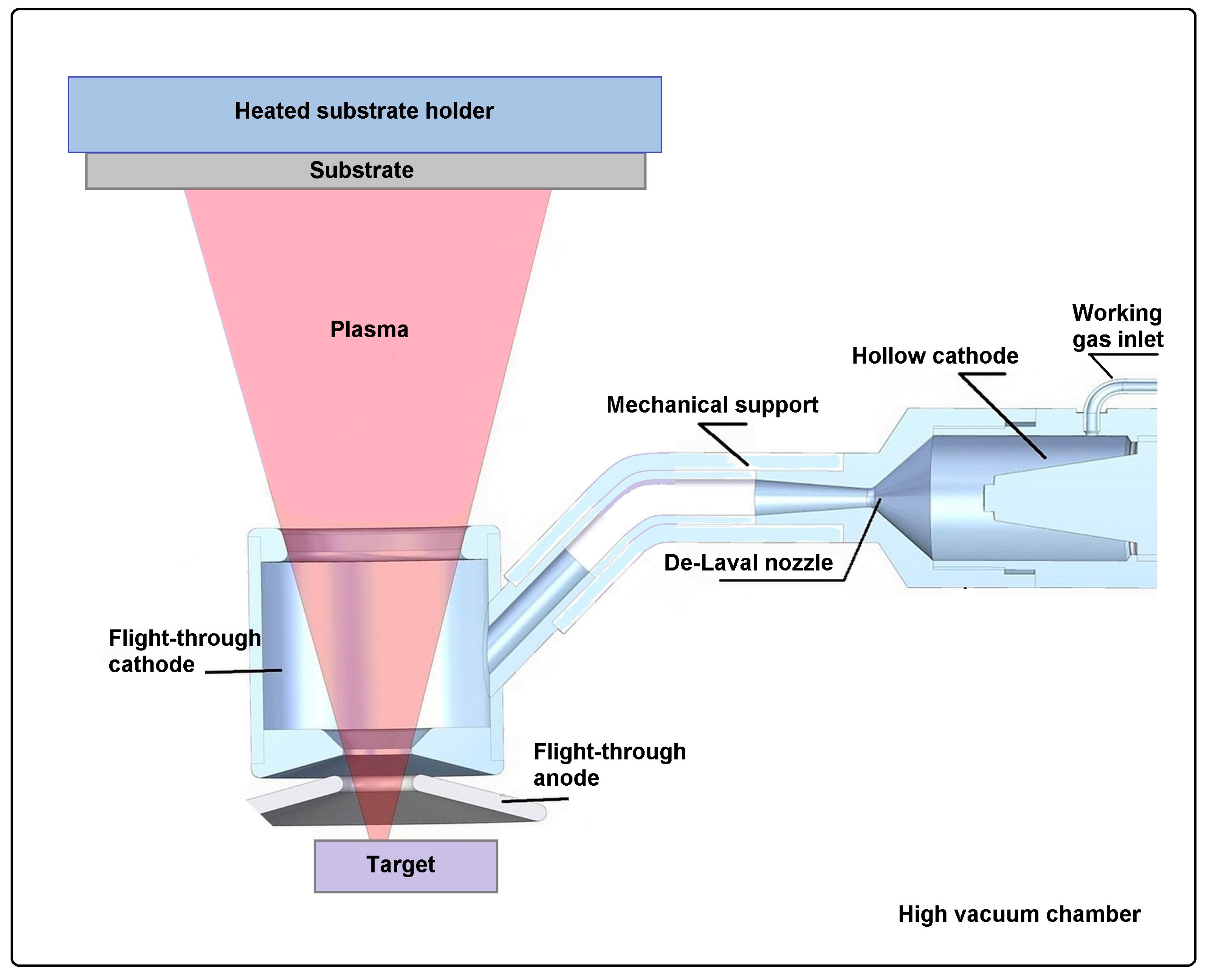
2. Materials and Methods

The films under study were deposited from an HfNbTiTaZr target of equimolar elemental composition, the preparation of which was as follows [19,20]: (i) arc melting of equimolar Hf, Nb, Ti, Ta, and Zr mixture (purity of the constitutive elements 99.5% wt.) performed under an inert gas (Ar) atmosphere; (ii) reactive metal atomization of the raw ingot obtained from the previous step by the electrode induction melting inert gas atomization (EIGA) method; (iii) sintering of the obtained powder by the field-assisted spark plasma sintering (SPS) performed for 2 min at temperature 1200 °C and pressure 80 MPa. The crystalline structure of the target obtained from X-ray diffraction data consisted of a single BCC phase [19] with the lattice parameter a = 3.40835(2) Å, confirming the HEA character of the alloy. For the subsequent IJD depositions, the ingot bulk was machined to the shape of a cylinder with a diameter of 35 mm and thickness of 5 mm.
The IJD method belongs to the family of physical vapor deposition (PVD) methods used in the preparation of thin films. It employs a pulsing high-energy electron beam to ablate the source target material through application of the so-called hollow cathode effect. The material to be deposited is converted into the form of an ionized plasma plum, which is then accelerated towards the deposition substrate (see, e.g., references [21,22,23] for overview of the basic physical principles the IJD method is built on). The practical strength of the IJD method consists in its high flexibility concerning the selection of working material (allowing for deposition of various complex materials such as dielectrics, high-temperature superconductors, and polymers [24,25,26,27]), well-defined stoichiometry transfer ratio between the target and the growing layer tunable by the electric parameters of the deposition process, a low thermal load of the deposited material, and the general ease of upscaling the deposition process by increasing the number of IJD heads simultaneously installed in the deposition chamber. The basic set of adjustable parameters supporting IJD flexibility involves the distance between the target and the substrate, the electric potential and frequency of the IJD source pulses, the temperature of the substrate, the type and pressure of the selected working gas, and total deposition time.
The studied samples were prepared using the experimental IJD system JetDep 100, installed in the laboratories of the Department of Solid State Engineering, Faculty of Nuclear Science and Physical Engineering of the Czech Technical University in Prague. The system was designed and fabricated in co-operation with Czech Vacuum, s.r.o. (Czech Republic) and Noivion s.r.l. (Italy). The scheme of the system is shown in Figure 1.
The chain of processes the IJD source uses starts with the working gas entering the hollow cathode cavity (also called the “trigger,” cf. Figure 1). Here, the primary plasma and electrons are created by an electric arc ignited by the modulated potential applied between the central electrode and the trigger outer wall. The plasma then expands and propagates towards the inner space of a flight-through cathode (also called the “transmitron”) through the attached de Laval nozzle. The transmitron starts to behave as an ordinary hollow cathode, with the oscillating primary electrons creating secondary electrons by avalanche ionization of the working gas. The working gas guided through the trigger, the de Laval nozzle, and the transmitron to the target then creates a conducting channel meeting Paschen’s law for electric discharge [22].
When enough electrons are generated in the transmitron by the hollow cathode effect, the electrons escape towards the target. The complex interaction of electrons and ions inside the plasma channel then creates two adjacent plasma regions forming together a “double layer” of opposite charges located in the vicinity of the transmitron opening. At the double-layer boundary, all the potential difference between the target and the transmitron is realized. Electrons propagating from the transmitron towards the target cross the electric double layer, are accelerated by its potential difference, and cause ablation of the target material.
The ablation is a rather fast, explosion-like process of quantum energy transfer to the target material. The ablated target material is in plasma state and expands through the transmitron away from the target surface, towards the substrate where it is deposited. The deposition process and redistribution of the growing film mass on the substrate surface is governed by a set of physical and chemical processes and parameters including, e.g., substrate–plasma ion interaction, the type of crystal structure of the substrate and target material, and the kinetic energy, temperature, and ionized state of the plasma ions. The homogeneity of the resulting film also depends significantly on the actual distance between the target and the substrate. If the distance is too short, the plasma retains too much kinetic energy at its arrival at the substrate surface and may cause damage to the substrate and/or to the already deposited film. Conversely, if the distance is too long, the plasma can condense during its travel to the substrate and deposit in the form of droplets.
The studied sample layers (reported further on as S16, S18, S20, and S22) consisted of 10 mm-wide, mutually separated strips on a pre-cleaned stainless steel substrate (50 × 50 mm2). The layers were prepared by using the IJD acceleration voltage (in kV) corresponding to the number indicated in the sample designation. The other main IJD deposition parameters were selected as follows: IJD pulsing head frequency 20 Hz, temporal pulse width 500 ns, mean electric current per pulse 2 kA, distance between the target and the substrate 90 mm, total deposition time 20 min per layer, working gas (Ar) pressure 130 mPa, and the substrate kept at room temperature (RT). During the whole deposition process, the target was rotated below the IJD head to reduce its local energy exposure and compromise the influence of possible local fluctuations in its chemical composition.
The searched IJD transport coefficients characterizing the transfer of individual elements between the target and the growing layer were calculated by dividing the mean chemical composition (in at. %) of the prepared layer by the mean composition of the deposition target. Due to the applied target rotation and the overall small volume of material ablated from the target during deposition of the tested layers, we neglected to change the target composition during deposition. The necessary elemental composition data were obtained by the energy dispersive X-ray spectroscopy (EDXS) method. The EDXS measurements were performed on a JEOL JSM-IT500HR scanning electron microscope (SEM), which was also applied to characterize the surface morphology of the prepared layers. With an accelerating voltage of 10 kV, the EDAX Octane Elite Super energy dispersive analyzer and secondary electron imaging mode were used. The thickness of the prepared layers was tested by the confocal microscopy (CM) method, using the laser confocal microscope LEXT OLS5000 (Olympus). The crystallographic phase composition of the prepared layers was checked by the X-ray diffraction (XRD) method. The measurements were performed in grazing incidence geometry on the X’Pert PRO MPD (Malvern Panalytical) diffractometer with the X’Cellerator detector, filtered CoKα radiation (λ = 1.79026 Å), and the grazing angle of the primary beam relative to the sample plane set to 1.5 angular degrees. The lattice parameters of the observed crystallographic phases were calculated using the standard Rietveld procedure implemented in the SW tool HighScore (Malvern Panalytical).

3. Results and Discussion

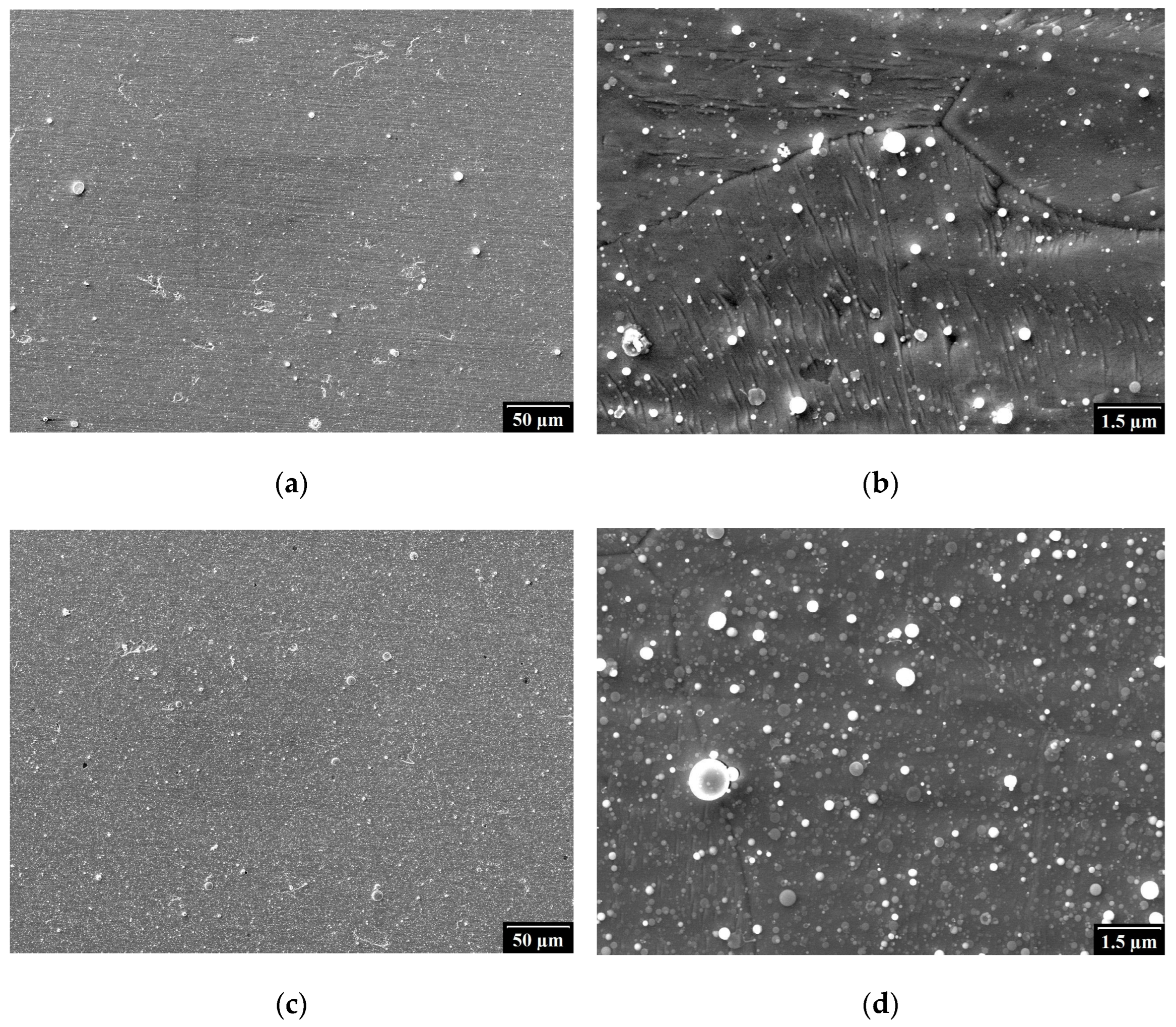
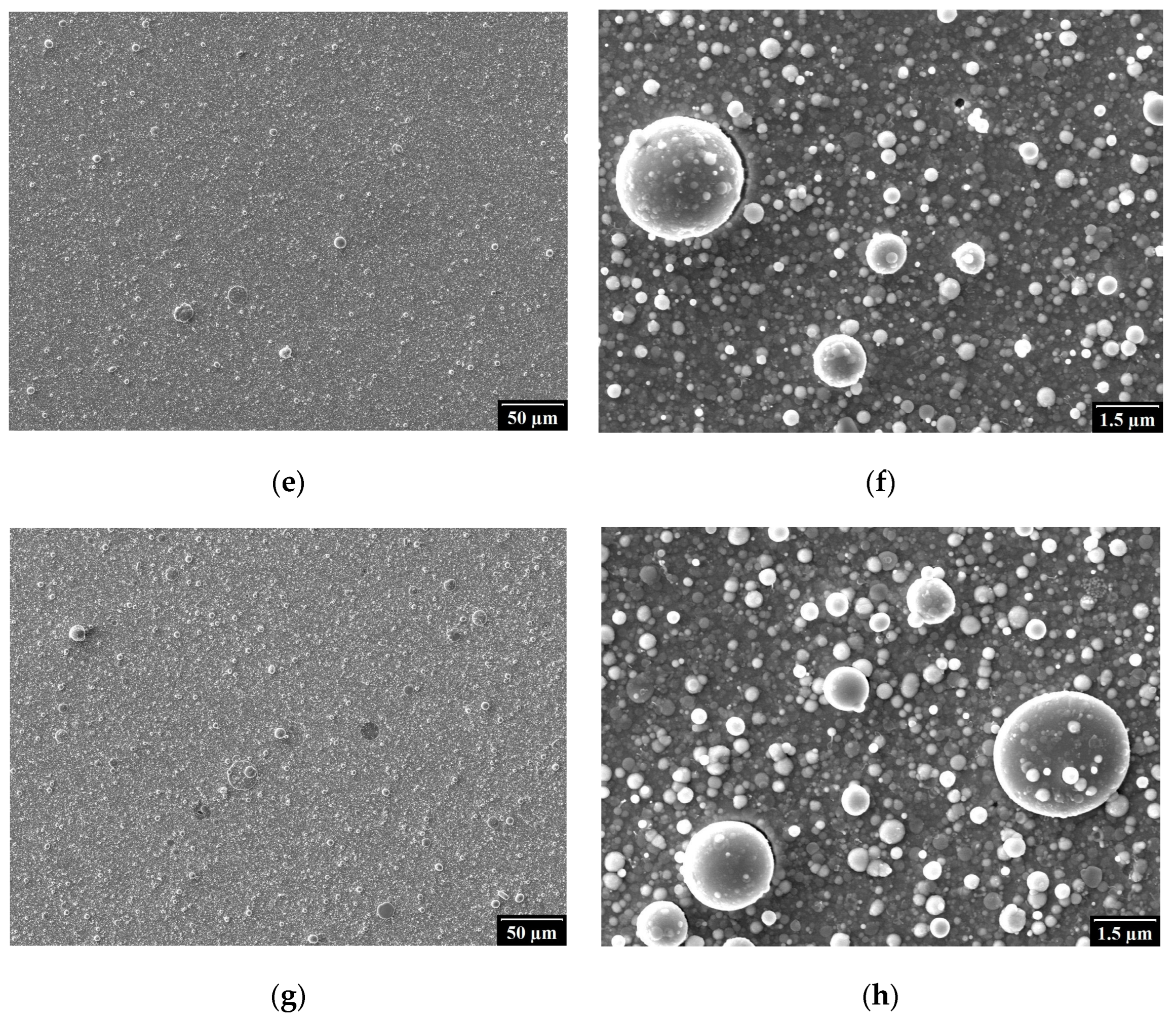
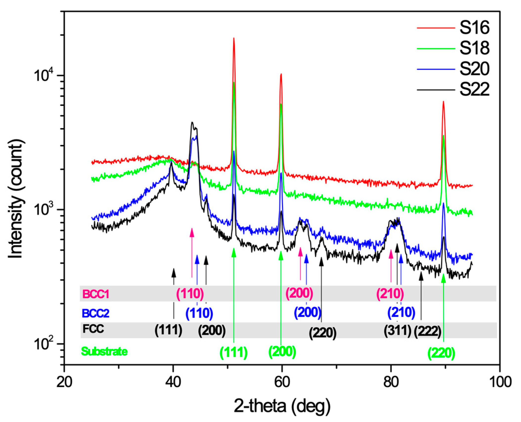
3.1. Morphology and Phase Composition of the Sample Layers

The overall thickness of the prepared layers obtained by CM measurement is given in Table 1. As expected, the thickness increases with the IJD accelerating voltage (U), in agreement with the increasing rate of the target mass ablation caused by the growing pulse power. The large standard deviations of the determined thickness are caused by the frequent particle-like surface corrugations discussed in detail below.
The evolution of the surface morphology of the prepared layers with the IJD accelerating voltage is demonstrated in Figure 2. With the U-value increasing, both the surface density and the average size of the observed splash-like surface irregularities increases. Within the tested voltage range, the highest surface smoothness is obtained for U = 16 kV. The occurrence of splashes is attributed to the impact of melted material clusters ejected from the deposition target.
The observed XRD patterns shown in Figure 3 document the evolution of phase composition for the studied samples. Apparently, the phase resolution increases with the layer thickness growing. With the layer thickness growing, the presence of the amorphous phase is becoming more pronounced, demonstrated by a broad maximum found in the low scattering angle region of the recorded patterns. The sharp peaks then correspond to the presence of the following three crystalline phases: BCC1 with the lattice parameter (a) in the range 3.410 and 3. 416 Å, BCC2 with a between 3.343 and 3.347 Å, and FCC with a ≈ 4.56 Å. The phase content given in volume percent calculated by standard Rietveld analysis of the observed XRD patterns is for all tested samples summarized in Table 2. Note that due to the small thickness of the S16 sample, the individual phase content data obtained for this sample should be taken with caution.
Compared to the films prepared by magnetron sputtering without the presence of nitrogen, which are dominated by the amorphous phase [12], the films prepared by IJD show a significantly higher content in the crystalline BCC phase, although the amorphous phase fraction is also significant and exceeds 50 volume percent for the samples S18, S20, and S22. Similar to our experimental conditions, the substrate was kept at room temperature during the layers’ growth reported in [12]. The presence of two BCC phases with slightly different lattice parameters observed in our samples resembles the results reported by Málek et al. [20] for a bulk equimolar HfNbTaTiZr specimen sintered at 1400 °C. In that case, too, two different BCC phases with the lattice parameters a = 3.399(8) Å and a = 3.347(3) Å were identified and interpreted as belonging, respectively, to the bulk equimolar HfNbTaTiZr matrix and to the Nb- and Ta-rich dendritic precipitates. Instead of the FCC phase observed in our samples (belonging likely, according to the observed a-value, to TiC or TiO2 precipitates), an HCP phase was observed in [20] interpreted as consisting of Zr- and Hf-rich precipitates.

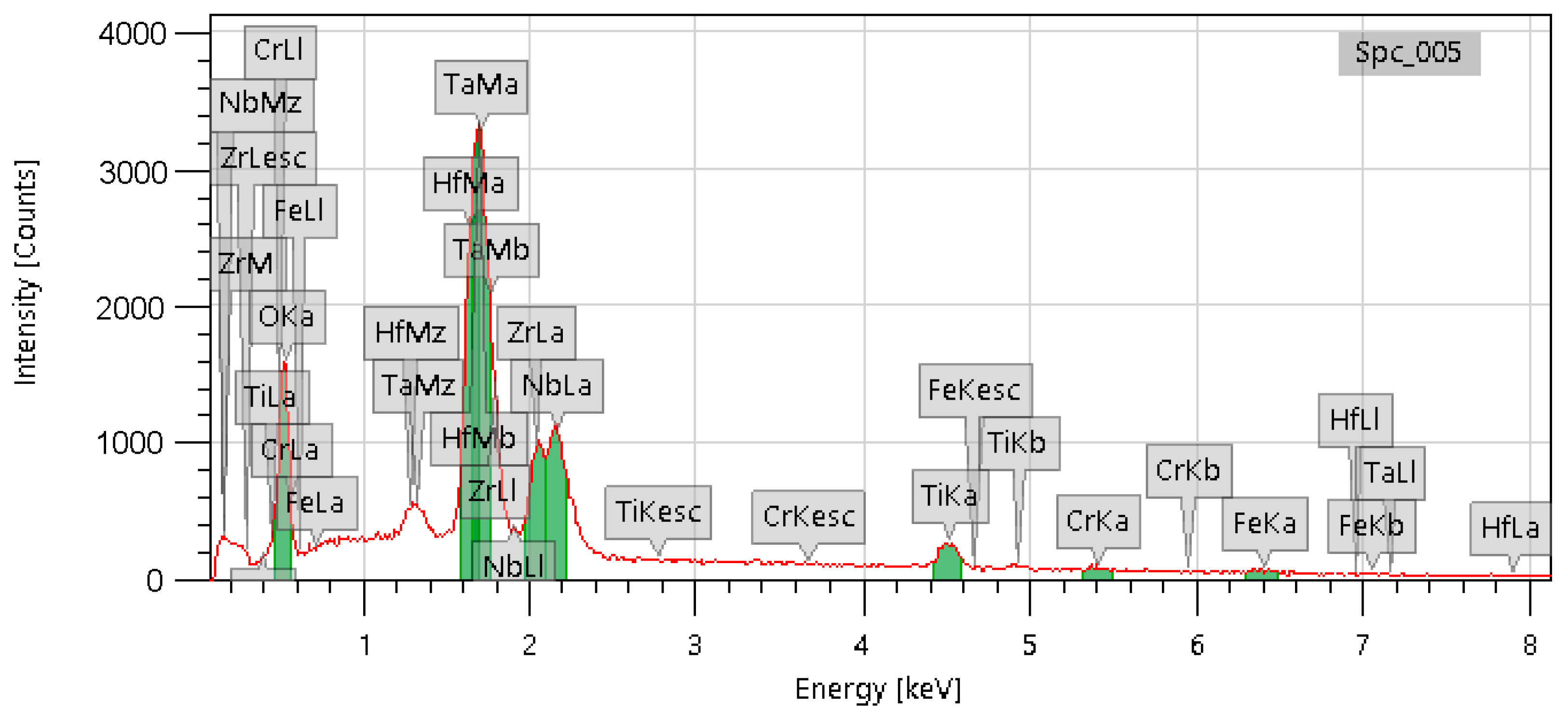
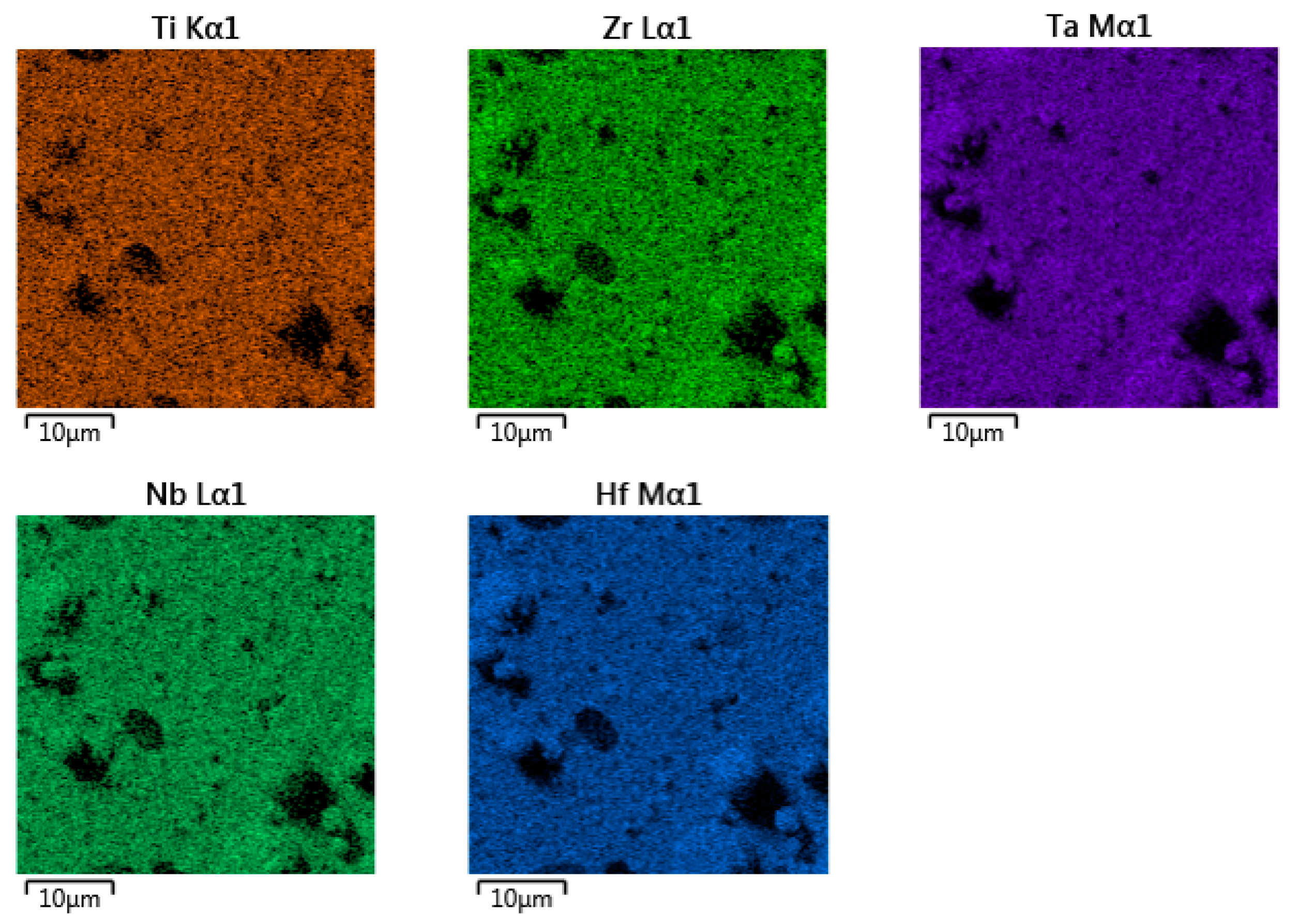
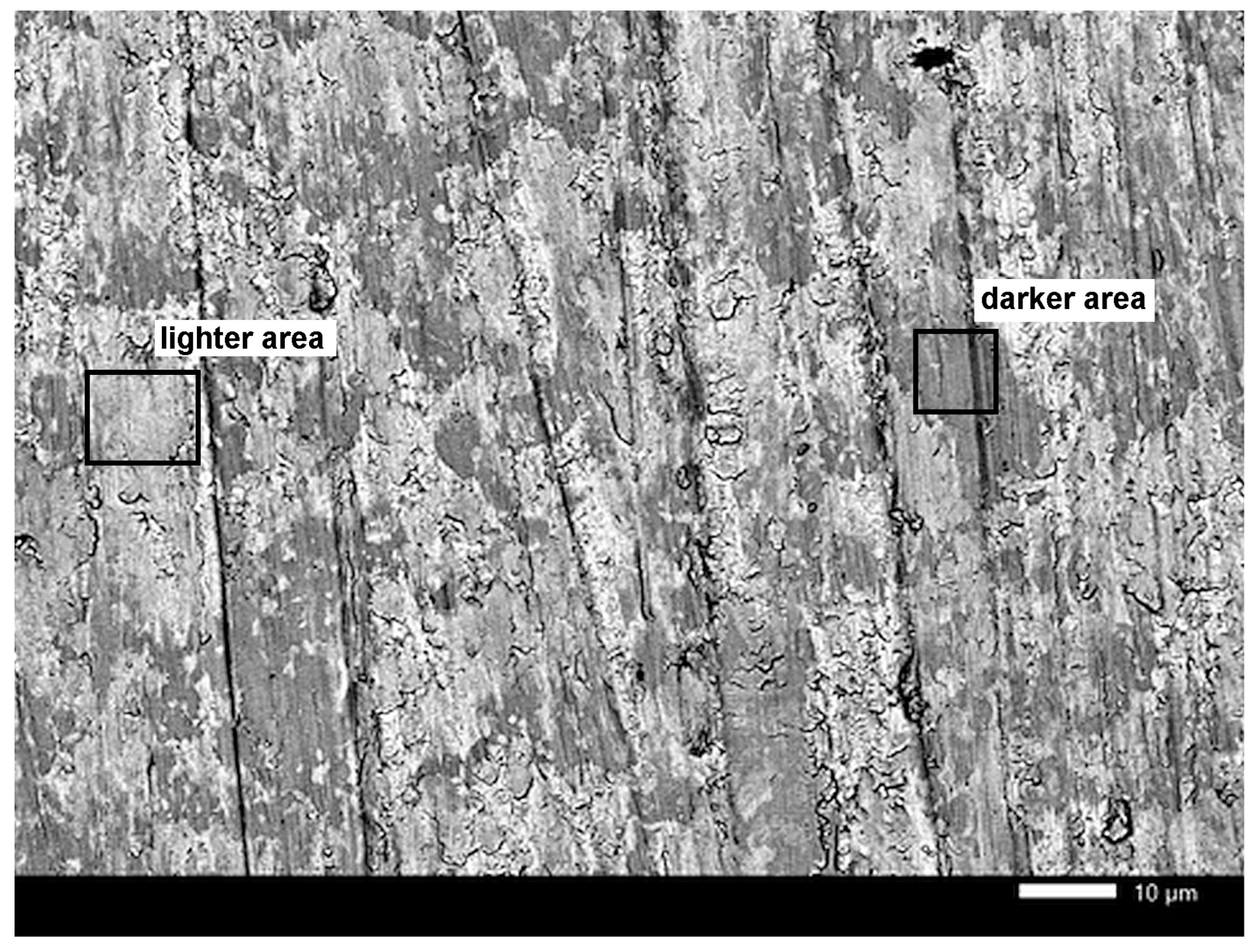
3.2. Chemical Composition and IJD Transport Coefficients

Following the observed elemental EDXS concentration maps, the constituting metallic elements are evenly distributed over the surface of the prepared layers for all the studied samples. As an example of the obtained EDXS data, Figure 4 and Figure 5 show, respectively, the typical EDXS spectrum and the elemental concentration maps observed for the sample S18. A significant amount of oxygen is also found in all tested layers (Figure 4), consistent with the amount found in the target (see below). Note that the oxygen content was not considered in the subsequent calculation of the transport coefficients.
To calculate the elemental transfer coefficients, a mean content of the constituting elements (Hf, Nb, Ta, Ti, Zr, c.f. Table 3) in the deposition target was considered. Not involved in these calculations is the content of oxygen, both in the target and in the prepared layers. Let us note that the mean target composition used here is effectively integrating over the two types of microstructural domains (Figure 6) of slightly different composition (Table 4) observed in the target, with characteristic dimensions of approx. 10–20 μm.
In order to obtain the representative composition data of the target, the EDXS measurements were performed at two depth levels below the target surface approached by successive grinding of the target mass. Four different lateral positions were then analyzed by EDXS at each of the ground levels. Usage of such mean values in calculation of the transfer coefficients is justified by (i) a large diameter of the minute ablation spot (amounting to several millimeters) compared to the above-mentioned typical structural domain size, and (ii) the steady target rotation applied during the deposition process, resulting in the total ablated area being widely spread over the deposition target surface.
The evolution of the mean elemental concentrations (determined from the obtained EDXS data by averaging over the sample surface) with the IJD accelerating voltage (U) is shown in Figure 7. With the U-value crossing 20 kV, the observed elemental concentrations of the constituting metallic elements tend to nearly monotonically converge upon the values ordered in size according to the atomic number (Z) of the element. The related IJD transport coefficients (the scale shown on the right side in Figure 7) take, for the IJD acceleration voltage of 22 kV, values between ca 0.77 and 1.2, centered upon the value of 1.0, corresponding to some ideal stoichiometry-preserving deposition process, and slightly above/below unity for the heavier (Hf, Ta)/lighter (Nb, Zr, Ti) elements, respectively. Interestingly, the order of elemental transfer coefficients observed for IJD is the opposite of that reported in ref. [4] for the films prepared by direct current magnetron sputtering, documenting thus the different physical nature of the two methods.
For the lower U-values, however, the dispersion in elemental transport coefficients is much broader (approx. 0.62–1.55 for U = 16 kV), allowing thus for controlling the elemental composition of films prepared by the IJD method, not only by changing the composition of the deposition target but also by varying the applied acceleration voltage of the IJD deposition head.

4. Conclusions

The obtained results document the main features of the IJD method and demonstrate the applicability of this method to deposition of thin films from the target composed of equimolar HfNbTiTaZr high-entropy alloy.
The surface morphology of the prepared layers is dominated by splash-like surface irregularities, the mean size and surface frequency of which increases with the applied IJD accelerating voltage. This undesirable effect can be later corrected by an appropriate choice of the distance between the target and the substrate, preventing the premature condensation of propagating plasma resulting in the creation of condensed clusters.
The phase composition of the layers is found to consist in four phases: amorphous phase, BCC1, BCC2, and FCC. The relative amount of the amorphous phase exceeds 50 vol. % for the layers prepared with the IJD accelerating U ≥ 18 kV. The lattice parameter found for the BCC1 phase is very close to that observed for the HEA solid solution of the HfNbTiTaZr target, so it is possible to conclude that at least some of the alloy forming the film mass retains the HEA character of the original bulk material.
The distribution of the constituting metallic elements in the plane of the prepared layers is uniform for all applied IJD voltages, without the resolvable presence of microstructural domains characterized by a slightly different elemental composition, observed in the volume of the deposition target.
The atomic concentration of the metallic elements in the prepared layers changes with the applied IJD accelerating voltage, its dispersion being most pronounced for the lowest applied voltage (16 kV). With the IJD voltage rising, the atomic concentrations converge smoothly to the values ordered, at the high-voltage limit (22 kV), in accordance with the atomic number of the present metallic elements.
The calculated elemental transfer coefficients between the target and the grown layer show significant changes over the whole interval of the tested accelerating voltages, with the largest variance for U = 16 kV (approx. 0.62–1.55) and the smallest one for U = 22 kV (approx. 0.77–1.2). For the set of metallic elements tested, and for the highest IJD voltage used in this work, the IJD elemental transfer coefficient is growing with the atomic number of the element. This observed voltage dependence of the elemental transfer coefficients can thus provide a flexible tool for fine-tuning the final atomic concentration of the prepared layer by varying the acceleration voltage of the IJD head. For HEA materials in particular, such a technique can be used to obtain sets of layers providing “composition libraries” relevant for the particular studied HEA system, prepared on a single substrate.

Author Contributions

Conceptualization, L.K.; methodology, J.Č. (Jaroslav Čech), J.Č. (Jiří Čapek), and K.T.; validation, L.K. and J.S.; formal analysis, L.K.; investigation, J.Č. (Jaroslav Čech), J.Č. (Jiří Čapek) and K.T.; resources, L.K.; data curation, J.Č. (Jaroslav Čech), J.Č. (Jiří Čapek) and K.T.; writing—original draft preparation, L.K.; writing—review and editing, L.K.; visualization, J.Č. (Jaroslav Čech), J.Č. (Jiří Čapek) and K.T.; supervision, L.K.; project administration, L.K.; funding acquisition, L.K. All authors have read and agreed to the published version of the manuscript.

Funding

This research was funded by the Ministry of Education, Youth and Sports of the Czech Republic grant number grant CZ.02.1.01/0.0/0.0/16_019/0000778, Czech Science Foundation grant GA21-05259S, and the Grant Agency of the Czech Technical University in Prague, grant No. SGS22/183/OHK4/3T/14.

Institutional Review Board Statement

Not applicable.

Informed Consent Statement

Not applicable.

Data Availability Statement

Data available from the authors upon the personal request.

Conflicts of Interest

The authors declare no conflict of interest. The funders had no role in the design of the study; in the collection, analyses, or interpretation of data; in the writing of the manuscript; or in the decision to publish the results.

References

  1. Senkov, O.N.; Scott, J.M.; Senkova, S.V.; Miracle, D.B.; Woodward, C.F. Microstructure and room temperature properties of a high-entropy TaNbHfZrTi alloy. J. Alloys Compd. 2011, 509, 6043–6048. [Google Scholar] [CrossRef]
  2. Senkov, O.N.; Scott, J.M.; Senkova, S.V.; Meisenkothen, F.; Miracle, D.B.; Woodward, C.F. Microstructure and elevated temperature properties of a refractory TaNbHfZrTi alloy. J. Mater. Sci. 2012, 47, 4062–4074. [Google Scholar] [CrossRef]
  3. Zýka, J.; Málek, J.; Pala, Z.; Andršová, I.; Veselý, J. Structure and mechanical properties of TaNbHfZrTi high entropy alloy. In Proceedings of the Metal 2015—24th International Conference on Metallurgy and Materials, Brno, Czech Republic, 3–5 June 2015. [Google Scholar]
  4. Lukáč, F.; Hruška, P.; Cichoň, S.; Vlasák, T.; Čížek, J.; Kmjec, T.; Melikhova, O.; Butterling, M.; Liedke, M.O.; Wagner, G. Defects in thin layers of high entropy alloy HfNbTaTiZr. Acta Phys. Pol. 2020, A137, 219–221. [Google Scholar] [CrossRef]
  5. Moore, C.M.; Wilson, J.A.; Rushton, M.J.D.; Lee, W.E.; Astbury, J.O.; Middlenurgh, S.C. Hydrogen accommodation in the TiZrNbHfTa high entropy alloy. Acta Mater. 2022, 229, 117832. [Google Scholar] [CrossRef]
  6. Senkov, O.N.; Wilks, G.B.; Miracle, D.B.; Chuang, C.P.; Liaw, K. Refractory high entropy alloys. Intermetallics 2010, 18, 1758–1765. [Google Scholar] [CrossRef]
  7. Senkov, O.N.; Wilks, G.B.; Scott, J.M.; Miracle, D.B. Mechanical properties of Nb25Mo25Ta25W25 and V20Nb20Mo20Ta20W20 refractory high entropy alloys. Intermetallics 2011, 19, 698–706. [Google Scholar] [CrossRef]
  8. Zýka, J.; Málek, J.; Veselý, J.; Lukáč, F.; Čížek, J.; Kuriplach, J.; Melikhova, O. Microstructure and Room Temperature Mechanical Properties of Different 3 and 4 Element Medium Entropy Alloys from HfNbTaTiZr System. Entropy 2019, 21, 114. [Google Scholar] [CrossRef] [Green Version]
  9. Zherebtsov, S.; Yurchenko, N.; Shaysultanov, D.; Tikhonovsky, M.; Salishchev, G.; Stepanov, N. Microstructure and Mechanical Properties Evolution in HfNbTaTiZr Refractory High-Entropy Alloy During Cold Rolling. Adv. Eng. Mater. 2020, 22, 2000105. [Google Scholar] [CrossRef]
  10. Stepanov, N.D.; Yurchenko, N.Y.; Zherebtsov, S.V.; Tikhonovsky, M.A.; Salishchev, G.A. Aging behavior of the HfNbTaTiZr high entropy alloy. Mater. Lett. 2018, 211, 87–90. [Google Scholar] [CrossRef]
  11. Farzaneh, A.; Khorasanim, M.; Farabi, E.; Gibson, I.; Leary, M.; Hossein Ghasemi, A.; Rolfe, B. Sandwich structure printing of Ti-Ni-Ti by directed energy deposition. Virtual Phys. Prototyp. 2022, 17, 1006–1030. [Google Scholar] [CrossRef]
  12. Hruška, P.; Lukáč, F.; Cichoň, S.; Vondráček, M.; Čížek, J.; Fekete, L.; Lančok, J.; Veselý, J.; Minárik, P.; Cieslar, M.; et al. Oxidation of amorphous HfNbTaTiZr high entropy alloy thin films prepared by DC magnetron sputtering. J. Alloy. Compd. 2021, 869, 157978. [Google Scholar] [CrossRef]
  13. Feng, X.; Zhang, K.; Zheng, Y.; Zhou, H.; Wan, Z. Chemical state, structure and mechanical properties of multi-element (CrTaNbMoV)Nx films by reactive magnetron sputtering. Mater. Chem. Phys. 2020, 239, 121991. [Google Scholar] [CrossRef]
  14. Zhang, X.; Pelenovich, V.; Liu, Y.; Ke, X.; Zhang, J.; Yang, B.; Ma, G.; Li, M.; Wang, X. Effect of bias voltages on microstructure and properties of (TiVCrNbSiTaBY)N high entropy alloy nitride coatings deposited by RF magnetron sputtering. Vacuum 2022, 195, 110710. [Google Scholar] [CrossRef]
  15. Li, H.; Jiang, N.; Li, J.; Huang, J.; Kong, J.; Xiong, D. Hard and tough (NbTaMoW)Nx high entropy nitride films with sub-stoichiometric nitrogen. J. Alloy. Compd. 2021, 889, 161713. [Google Scholar] [CrossRef]
  16. Hsieh, T.H.; Hsu, C.H.; Wu, C.Y.; Kao, K.O.; Hsu, C.Y. Effects of deposition parameters on the structure and mechanical properties of high-entropy alloy nitride films. Curr. Appl. Phys. 2018, 18, 512–518. [Google Scholar] [CrossRef]
  17. Chen, L.; Li, W.; Liu, P.; Zhang, K.; Ma, F.; Chen, X.; Zhou, H.; Liu, X. Microstructure and mechanical properties of (AlCrTiZrV)Nx high-entropy alloy nitride films by reactive magnetron sputtering. Vacuum 2020, 181, 109706. [Google Scholar] [CrossRef]
  18. Xia, A.; Dedoncker, R.; Glushko, I.; Cordill, M.J.; Depla, D.; Franz, R. Influence of the nitrogen content on the structure and properties of MoNbTaVW high entropy alloy thin films. J. Alloy. Compd. 2021, 850, 156740. [Google Scholar] [CrossRef]
  19. Lukac, F.; Dudr, M.; Musalek, R.; Klecka, J.; Cinert, J.; Cizek, J.; Chraska, T.; Melikhova, O.; Kuriplach, J.; Zyka, J.; et al. Spark plasma sintering of gas atomized high-entropy alloy HfNbTaTiZr. J. Mater. Res. 2018, 33, 3247–3257. [Google Scholar] [CrossRef]
  20. Málek, J.; Zýka, J.; Lukáč, F.; Čížek, J.; Kunčická, L.; Kocich, R. Microstructure and Mechanical Properties of Sintered and Heat-Treated HfNbTaTiZr High Entropy Alloy. Metals 2019, 9, 1324. [Google Scholar] [CrossRef] [Green Version]
  21. Metel, A.; Kolobov, V. Glow discharges with electrostatic confinement of fast electrons. J. Phys. D 2015, 48, 233001. [Google Scholar]
  22. Giacomo, G. Paschen’s law in extreme pressure and temperature conditions. IEEE Trans. Plasma Sci. 2019, 47, 1641–1647. [Google Scholar]
  23. Müller, G.; Konijnenberg, M.; Krafft, G.; Schultheiss, C. Thin film deposition by means of pulsed electron beam ablation. In Science and Technology of Thin Films; Matacotta, F.C., Ottaviani, G., Eds.; World Scientific: London, UK, 1995; pp. 89–119. [Google Scholar]
  24. Skočdopole, J.; Lojka, M.; Hlásek, T.; Antončík, F.; Jankovský, O.; Kalvoda, L. Influence of Substrate Temperature on the Morphology and Phase Composition of Thin Films Prepared From Y-123 Targets by the IJD Method. IEEE Trans. Appl. Supercond. 2023, 33, 7500604. [Google Scholar] [CrossRef]
  25. Skočdopole, J.; Lojka, M.; Hlásek, T.; Antončík, F.; Jankovský, O.; Kalvoda, L. Transport Coefficients in Y-Ba-Cu-O System for Ionized Jet Deposition Method. IEEE Trans. Appl. Supercond. 2021, 31, 9364744. [Google Scholar] [CrossRef]
  26. Skočdopole, J.; Aversa, L.; Golan, M.; Schenk, A.; Baldi, G.; Kratochvilova, I.; Kalvoda, L.; Nozar, P. Preparing of the chameleon coating by the ion jet deposition method. Acta Polytech. CTU Proc. 2017, 9, 19–25. [Google Scholar] [CrossRef] [Green Version]
  27. Skočdopole, J.; Kalvoda, L.; Nozar, P.; Netopilík, M. Preparation of polymeric coatings by ionized jet deposition method. Chem. Pap. 2018, 72, 1735–1739. [Google Scholar] [CrossRef]
Figure 1. Scheme of the IJD deposition system JetDep100 used in preparation of the studied samples; the main construction parts are indicated (see text for details).
Crystals 13 00580 g001
Figure 2. SEM micrographs of samples S16 (a,b), S18 (c,d), S20 (e,f), and S22 (g,h); the magnification of images on the left and right side set to 300× and 10,000×, respectively; the incident electron beam voltage 100 kV and secondary electrons imaging mode used.
Crystals 13 00580 g002aCrystals 13 00580 g002b
Figure 3. XRD patterns observed for the studied samples S16–S22; the background levels shifted for clarity; the crystalline phase symbols, angular positions, and Miller indices of the diffraction maxima are indicated.
Crystals 13 00580 g003
Figure 4. Example of the observed EDXS intensity patterns; sample S18; symbols of elements and X-ray fluorescence transitions are shown.
Crystals 13 00580 g004
Figure 5. Example of the elemental surface concentration maps obtained by EDXS; sample S18; symbols of the elements and characteristic X-ray fluorescence lines used in the measurements are shown.
Crystals 13 00580 g005
Figure 6. SEM micrograph of the ground deposition target surface; 10 kV, back-scattered electrons, magnification 1000×; the presence of “light” and “dark” structural domains is apparent; the straight scratch- lines are caused by the applied grinding process.
Crystals 13 00580 g006
Figure 7. Influence of the applied IJD accelerating voltage on the resulting elemental composition of the grown film (vertical scale on the left side; only the elements listed in the legend are considered) and the corresponding calculated IJD transport coefficient (vertical scale on the right side).
Crystals 13 00580 g007
Table 1. Mean thickness of the sample layers as obtained from CM measurements; values determined as the average of four measurements taken at different locations on the tested layer.
SampleAccelerating Voltage U (kV)Mean Thickness (nm)
S161674 ± 25
S1818178 ± 32
S2020364 ± 51
S2222559 ± 119
Table 2. Phase composition (volume %) of the studied layers obtained by XRD phase analysis with the substrate contribution subtracted.
PhaseS16S18S20S22
Amorphous phase26.5 ± 15.149.8 ± 11.864.5 ± 7.556.4 ± 4.3
BCC151.1 ± 29.219.1 ± 4.513.8 ± 1.627.5 ± 2.1
BCC215.5 ± 8.928.2 ± 6.718.4 ± 2.114.0 ± 1.1
FCC6.8 ± 3.92.9 ± 0.72.5 ± 0.32.0 ± 0.2
Table 3. Mean elemental composition of the deposition target obtained by EDXS. Only the content of the constituting metallic elements is included.
ElementZConcentration (at. %)
Ti2122.1 ± 0.9
Zr4019.6 ± 0.3
Nb4118.7 ± 0.9
Hf7220.8 ± 0.6
Ta7318.7 ± 0.8
Table 4. Elemental composition observed by EDXS on a pair of the “light” and “dark” structural domains shown in Figure 6; the oxygen content is included.
ElementConcentration, Darker
Domain (at. %)
Concentration, Lighter
Domain (at. %)
Ti26.913.1
Zr21.716.8
Nb13.515.6
Hf19.917.0
Ta10.722.8
O7.312.8
Disclaimer/Publisher’s Note: The statements, opinions and data contained in all publications are solely those of the individual author(s) and contributor(s) and not of MDPI and/or the editor(s). MDPI and/or the editor(s) disclaim responsibility for any injury to people or property resulting from any ideas, methods, instructions or products referred to in the content.

