1. Introduction
Optical bistability (OB) is a nonlinear optical phenomenon, in which the single-value input intensity is directly relevant to two different transmission intensities, and the input-output intensity relationship is shown as a hysteresis curve [
1,
2,
3]. This effect can be applied to multiple components, such as all-optical switches, optical logic devices, optical differential amplifiers, optical diodes, and other elements with extremely fast and controllable function [
4,
5,
6]. Therefore, optical bistable devices have a promising prospect in all optical communication, optical information processing, and optical computing. In bistability, with the increase in inputting light intensity, the outputting intensity of light jumps upward abruptly at the upper threshold, while with the intensity decrease in incident lights, the output jumps downward at the lower threshold. In other words, the intensity of the incident light triggers the transmitted light to produce a step effect. The incident light intensity at the jump points is called the upper threshold and the lower threshold of OB, respectively. Previous studies have shown that OB can be realized in many structures and materials, such as the nonlinear prism couplers [
7,
8], semiconductors [
9], Fano resonances [
10], Fabry–Perot cavities [
11], and ring resonators [
12]. For optical equipment, it is extremely important to realize the dynamic adjustment of OB. Graphene, as a new two-dimensional material, has both metallic and non-metallic properties. Furthermore, it possesses an ultra-fast and broadband response, low optical loss, and tunability of the surface conductivity [
13,
14]. Especially, graphene has a strong nonlinear characteristic which can be utilized for OB [
15,
16] and OB based on photonic crystal (PC) heterostructure/nonlinear graphene as well [
17,
18]. OB also could be realized based on topological edge states, one-dimensional resonant PCs, the tight-binding model multilayer graphene system, and complex photonic lattices [
19,
20,
21,
22,
23]. These studies can effectively reduce and tune the threshold of OB. It is a still a challenge, despite the fundamental principle of realizing the OB phenomenon being perfectly clear, so at least the low threshold and simple structure are well planned.
Furthermore, superconducting PCs demonstrate many significative and special electromagnetic properties in striking contrast to the precedent conventional PCs [
24,
25,
26]. Researchers found that a series of transmission peaks emerge in the major photonic band gap, which is the counterpart of the local modes of light. The bandwidth is particularly susceptible to the thickness of superconductors and environment temperature. Compared with the traditional dielectric PCs, the width of the photonic band gap changes regularly with the change in the width of the whole structure layers. All these characteristics promote the development of photoelectronic devices to be more efficient, such as multiplexers, optical fiber, filter, temperature sensing device, and other applications for optical communication [
27]. The superconductor and semiconductor are sensitive to the environment temperature. On the other hand, defect PCs can localize the electric field greatly. Therefore, it is meaningful to combine the superconductor and semiconductor with graphene to form a defect PC and to explore OB and its temperature dependence in this compound system.
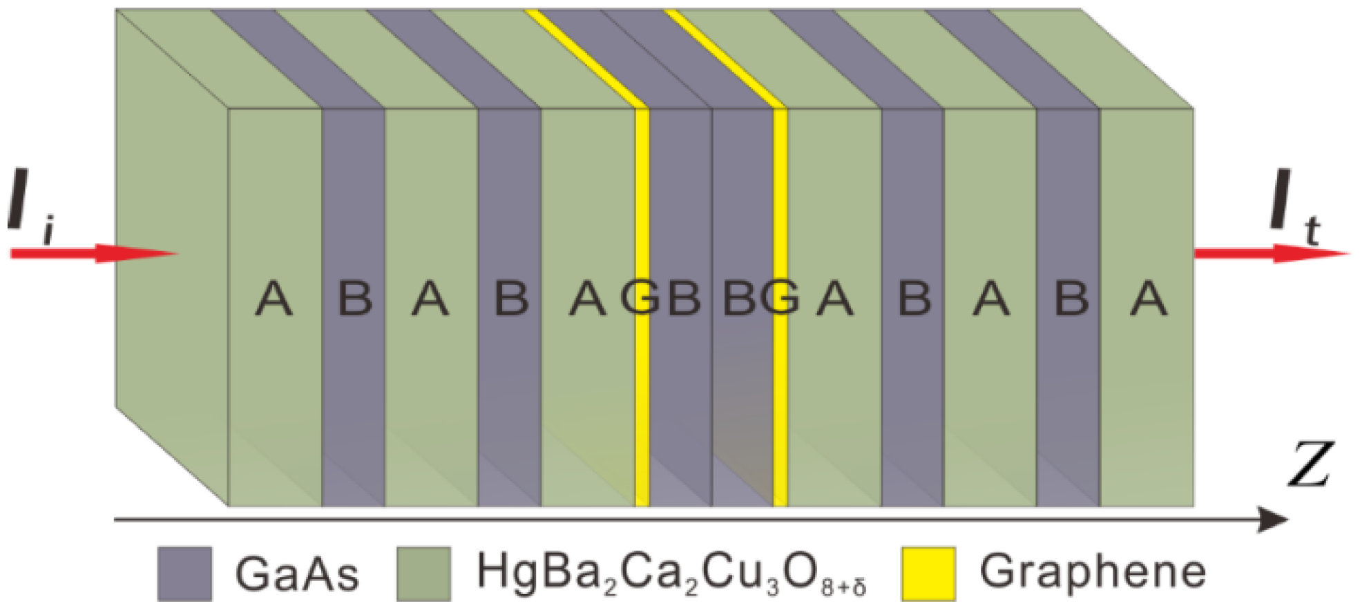
Optical bistability is studied in one-dimensional PCs embedded with graphene. The one-dimensional PC is formed by periodic arrangement of superconducting materials and semiconductor materials as well as graphene inlay. The defect modes in the transmission spectrum are presented. Low-threshold tunable OB phenomenon is then illustrated. Furthermore, the relationships between the bistable thresholds, threshold intervals, environment temperature, incident wavelengths, and the chemical potential of graphene are presented. Our work provides a new theoretical approach and inspiration for the study of tunable threshold OB in low-temperature environment and gives a scheme for temperature-controlled non-contact switches.
2. Theoretical Model and Method
Two kinds of medium sheet A and medium sheet B with distinct values in refractive index are arranged to form the one-dimensional PC. The substitution would be: S
1 = ABBA, S
2 = ABABBABA, ……, S
N = (AB)
N (BA)
N, where
N (
N = 1, 2, ……) is the number of spatial periods of the periodic structure, and
N is a positive integer. When
N tends to infinity, the structure is one-dimensional PC. When
N is finite, the structure is called truncated PC. Two truncated PCs (AB)
N and (BA)
N are combined to form a one-dimensional symmetric structure (AB)
N (BA)
N. For example,
N = 3, viz. the current structure is ABABABBABABA. Graphene G is embedded into the interface of the medium to form a composite structure (AB)
N−1AGBBGA(BA)
N−1. The schematic of composite structure consisting of superconducting materials, and graphene is shown schematically in
Figure 1. The structure is expressed as ABABABBGABABA. The symbol
Ii is the incident light, and
It is the transmitted light. Here, transverse magnetic (TM) polarized light waves are considered to impact the composition and propagate along the Z-axis.
The superconductor and semiconductor component layers can be manufactured by the chemical vapor deposition method which is a common technique in micro- and nano-fabrication. The primary superconducting and semiconducting layers arrange alternatively to satisfy the periodic sequence law. Graphene sheet on a substrate can also be transferred to the interface of two different layers [
28], so it is feasible to realize this proposed scheme in experiments completely.
The host materials of medium A and B are HgBa
2Ca
2Cu
3O
8+δ and GaAs, respectively. The superconductor HgBa
2Ca
2Cu
3O
8+δ is a lossless material as environment temperature is below the critical value, and its permittivity is given by
where
ω = 2π
f is the angular frequency of the incident light waves, and
f =
c/
λ is the frequency. The London penetration depth
λL can be expressed as
where
λ0 = 6.1 μm, and
Te is the environment temperature. The critical temperature is
Tc = A
1 + B
1P + D
1P2, A
1 = 134, B
1 = 2.009, D
1 = −4.194 × 10
−2, and the symbol of
P represents the hydrostatic pressure applied on the superconductor [
29,
30].
The superconductor HgBa
2Ca
2Cu
3O
8+δ is anisotropic, and experimental results demonstrate that the maximum London penetration depth are
λab0 = 0.21 μm and
λc0 = 6.1 μm, respectively [
29]. Here in our proposed system, the HgBa
2Ca
2Cu
3O
8+δ layers are local in the ab-plane (or XY-plane) and arrange along the c-axis (or Z-axis); meanwhile, the incident light waves are TM-polarized and normally impinge upon the structure from the left, propagating along the c-axis (or Z-axis). Therefore, the parallel component (along the Z-axis) of permittivity of HgBa
2Ca
2Cu
3O
8+δ which is governed by
λc determines the optical wave propagating, and the maximum penetration depth is
λ0 =
λc0.
The dielectric constant of the semiconductor material GaAs is
where K is the absolute temperature unit;
P is the hydrostatic pressure [
30,
31].
The relationship between the thickness of medium sheet B and the pressure is
where
db0 is the initial thickness of
P = 0; the elastic constant is
M11 = 1.16 × 10
−2 GPa
−1, and
M12 = −3.7 × 10
−3 GPa
−1 [
32,
33].
The hydrostatic pressure
P on sheet B can make it strain, which is an elastic distortion, with stretching and shrinking in size of the sheet. The layer A also distorts elastically, but elastic constant of material A is one order magnitude lower than the value of material B [
33]. Therefore, we neglect the influence of the hydrostatic pressure on the thickness of layer A.
Taking the environment temperature Te = 100 K, P = 0 Pa as the standard, the refractive index of HgBa2Ca2Cu3O8+δ is na0 = 0.9994; the refractive index of GaAs is nb0 = 3.5678, and λ = 1.55 μm. Based on this, the thickness of medium sheet A and medium sheet B is determined to be 1/4 optical wavelength, respectively; that is, the thickness of A is da = λ0/(4na0) = 0.3877 μm. The thickness of B is db = λ0/(4nb0) = 0.1086 μm.
The surface conductivity of graphene is
, which includes the intra-band transition and the inter-band transition of electrons [
34]. The first part is defined as
where
in this equation are, respectively, the electric charge, the Planck constant, the imaginary unit, and the Boltzmann constant. The parameter of
τ is the phenomenological relaxation time of electrons, and
μ is the chemical potential of graphene. When
,
, another part of the graphene conductivity can be represented as
The nonlinear conductivity coefficient of graphene is
whose Fermi velocity satisfies
VF ≈
c/300 [
35].
The equivalent dielectric constant of graphene is
Here the equivalent thickness of graphene is set as
dg = 0.33 nm, and
k0 represents the wave vector in vacuum. The symbol of
is the local electric field intensity at the position where graphene locates in Z-direction [
36,
37]. For a normally incident TM-polarized light wave, propagating along with the Z-axis, the magnetic fields contain the orthogonal components
Hx and
Hy, and the electric field only includes the parallel component
Ez. The third order nonlinearity of graphene is proportional to the local electric field intensity of the parallel component |
Ez|
2.
The one-dimensional photonic crystal layers including graphene arrange along the Z-axis. As light waves normally impinge upon the system from the left and transmit in each layer, one can simulate the linear transmission spectra through the forward transmission matrix method (FTMM) [
38,
39]. The electromagnetic fields at the incident port of systems are denoted by (
Ei,
Hi), and at the outputting port it is expressed as (
Eo,
Ho), of which their relationship is governed by
where
m11,
m12,
m21, and
m22, respectively, mean the four elements of transfer matrix. The subscript
γ represents the total layer number of structures. The transfer matrix of light waves
Mi in the
ith layer can is given by
For the non-magnetic medium, the transmission phase is φl = 2πdl(εl − sin2θ)/λ, where θ is the incident angle, and εl, dl, and λ are the permittivity, dielectric thickness, and the wavelength of the incident light, respectively. For a TM-polarized light wave, the light resistivity in each layer is given by ηl = εl(ε0/μ0)1/2/(εl − sin2θ)1/2.
The photonic crystal is placed in free space, and the transmission coefficients can be derived by the expression
where the vacuum resistivity for the incident, and outputting ports are
ηo =
ηi =
η0 = (
ε0μ0)
1/2, respectively. The transmittance of light waves is derived by
αT =
tt*.
The distribution of electric field and the optical bistability are simulated by the inverse transfer matrix method (ITMM) [
40]. We view graphene as an equivalent dielectric and denote it by the
lth layer. The transfer matrix of graphene contains the permittivity item
εl =
εg + 1 +
iσ0η0/
k0dg +
iσ3η0|
Ez,l|
2/
k0dg. It needs to give a nonlinear correction for the linear permittivity of graphene as a strong laser impinges upon this structure, especially in the process of simulating the optical bistability. We, respectively, set
Eo and
Ho =
Eo/
η0 as the electric field and the magnetic field at the outputting port. The total transfer matrix of the partial structure from the
l+1th layer to the last layer is given by [
m′11,
m′12;
m′21,
m′22], and the corresponding transmittance of light waves is denoted by
α′T. Then, the electric field at the incident port of the
l+1th layer is derived by |
Ez,l|
2 = |
Eo|
2/
α′T. The electric field distribution can also be calculated by dividing the superconductor and semiconductor layers into a series of slices in nm magnitude, ignoring the nonlinear correction term.
3. Results and Discussion
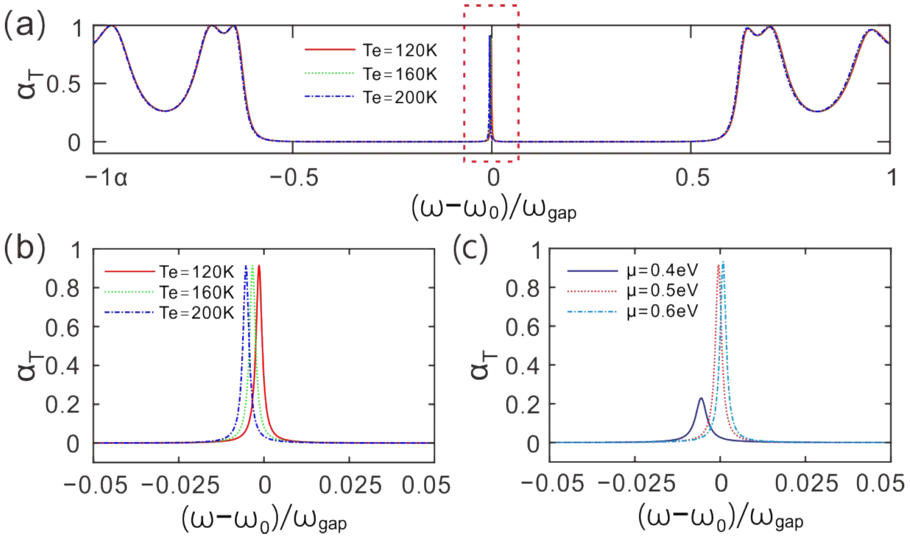
Figure 2a gives the transmission spectra for
N = 3,
μ = 0.5 eV,
= 0.15 ps. The transverse coordinate of (
ω −
ω0)/
ωgap is the normalized angular frequency, where
ω = 2πc/λ is the incident angular frequency of light;
ω0 = 2πc/
λ0 is the central angular frequency; arcsin represents the inverse sine function; and
ωgap = 4
ω0arcsin|(
na0 −
nb0)/(
na0 +
nb0)|
2/π is the photonic bandgap [
41]. The symbol of
αT is the transmittance of light waves.
Each environment temperature value corresponds to a light wave transmission spectrum curve. For (ω − ω0)/ωgap = (−1, 1), there is a photonic band gap in the middle of each transmission spectrum curve. In the middle of the band gap, there is a resonant transmission peak, such as the position marked by the dotted line. The central transmission mode of the band gap has a strong localization effect on the electric field. The main energy of the electric field is bound at the interface of the medium.
Figure 2b shows a local enlarged view of the transmission mode at the center of the band gap at different environment temperatures. One can see that the locations of the resonant transmission peaks corresponding to different environment temperatures are different. Obviously, the position of the resonance transmission peak moves to the left with the increase in the environment temperature value, such as the low-frequency direction. Different resonance peaks correspond to different resonance wavelengths; that is, the central wavelength corresponding to the transmission peak wanders towards the long wavelength as the temperature increases. Therefore, the position of transmission peak, i.e., transmission wavelength, can be controlled by different environment temperatures.
Figure 2c gives a local enlarged view of the central transmission mode of the band gap for different graphene chemical potentials. The chemical potential
μ can be tuned by the gate voltage
Vg on graphene, and their relation can be governed by [
42]
where the parameter
vF ≈ 10
6 m/s is the Fermi velocity of electrons in graphene;
a0 is empirical constant and is given by
a0 = 9 × 10
−16 m; and
VD is the offset bias voltage, and it is generally set as
VD = 0 for intrinsic graphene. We have added the discussion in the revised manuscript. The environment temperature is set to
Te = 100 K,
τ = 0.15 ps. It is obvious that the locations of transmission peaks corresponding to different chemical potentials are different. The position of the transmission peak moves to the left with the decrease in the chemical potential, that is, to the low frequency direction, while the central wavelength of the transmission peak changes to the long wavelength, and the peak transmittance will decrease. Therefore, the wavelength and transmittance of the central transmission mode can also be dominated by the chemical potential of graphene.
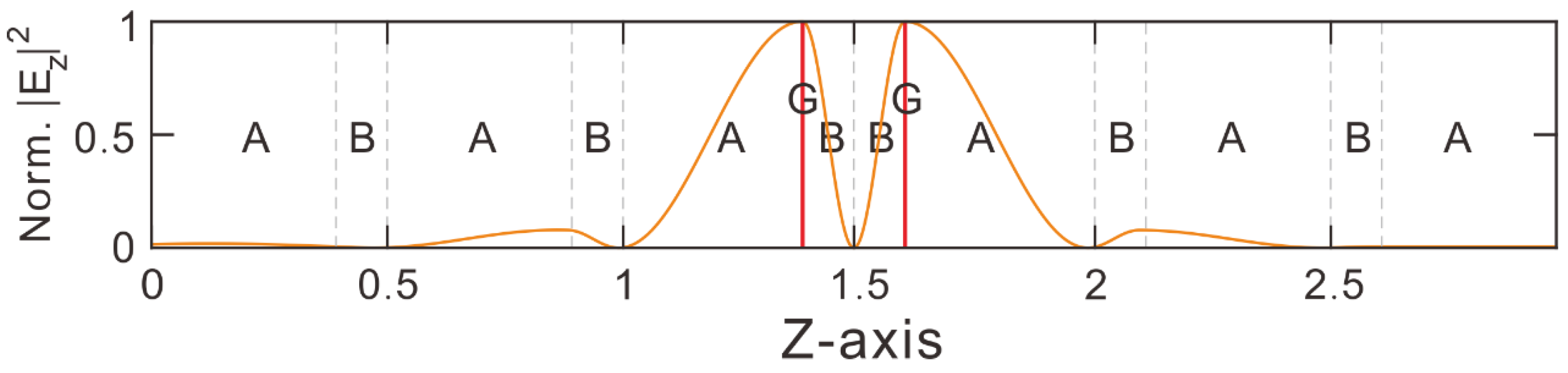
Figure 3 demonstrates the electric field distribution of the central transmission mode in the whole structure (
N = 3). Taking
Te = 100 K as an example, wavelength of central resonant mode is
λp = 1.5506 μm. The horizontal direction is the arrangement direction of the medium sheet. The ordinate represents the intensity of the component of the electric field in the horizontal direction and is normalized. One can be seen that the electric field is mainly distributed in the middle of the structure (denoted by the orange line), and the electric field intensity is the largest on the two media interfaces of AB and BA, respectively. Graphene (denoted by the red lines) is embedded on the two media interfaces between AB and BA, which have the largest electric field strength, forming a three-layer structure of AGB and BGA. The whole system structure is ABABABBGABABA. The local electric field strength at the location of graphene is the largest; the third-order nonlinear effect of graphene should be improved obviously so that the optical bistability with low threshold can be achieved.
The defect mode is a transmission mode in the transmission spectrum; on the other hand, it is also a localized optical mode for the longitudinal distributed field. We here give the stationary distribution of the longitudinal mode. It is similar to the mode field distribution of standing wave resonance, so the mode is static and time-free.
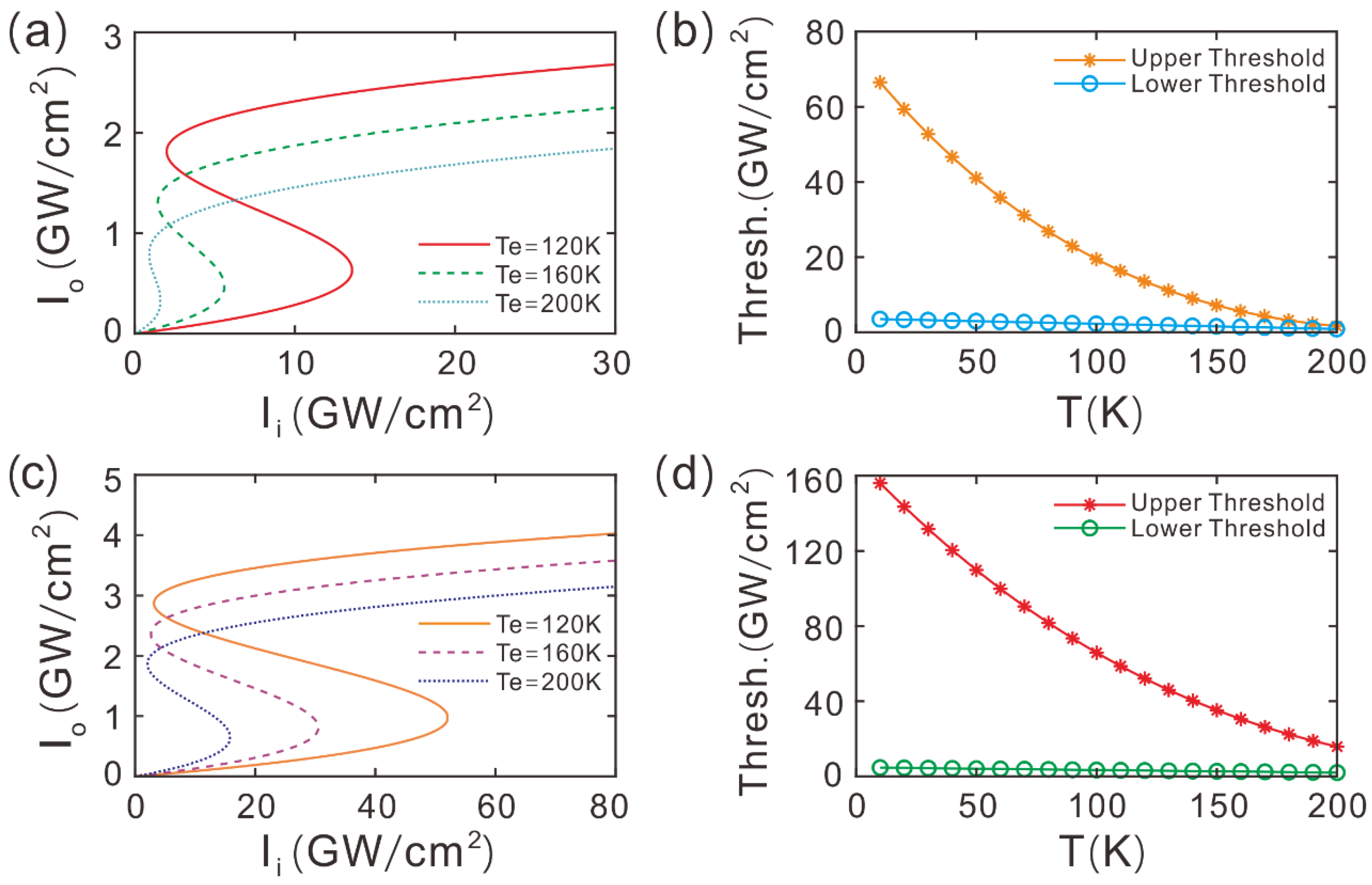
Figure 4a shows the input–output light intensity variation relationship under different environment temperatures for
λ = 1.56 μm, which is red-detuning to that
λ = 1.5506 μm in the linear spectrum. It is the condition for realizing OB. Other parameters remain unchanged. For different values of environment temperature, there are different input-output light intensity curves and in each curve; there is an S-shaped curve segment, which is the OB effect. The left and right inflection points of the S-shaped curve segment correspond to the lower threshold
Iid and the upper threshold
Iiu of the OB, respectively. As the value of
Ii gradually increases from a lower value to
Iiu, the value of
Io changes upward. As the value of
Ii gradually decreases from a higher value to
Iid, the value of
Io changes downward. The upper and lower thresholds of the corresponding OB are different at different values of environment temperature. As the value of
Ii changes, viz.
Iid <
Ii <
Iiu, one input can correspond to two stable outputs, which is the origin of the name of OB. The above OB is further applied to the temperature control switch. The upper threshold
Iiu corresponds to the opening threshold of the temperature control switch, and the lower threshold
Iid corresponds to the closing threshold of the temperature control switch. The turn-on threshold and turn-off threshold are functions of the environment temperature. Therefore, the turn-on and turn-off threshold of the switch are controlled by the environment temperature.
For a given environment temperature
Te = 120 K, the corresponding lower threshold and upper threshold are
Iid = 1.9902 GW/cm
2 and
Iiu = 13.5776 GW/cm
2, respectively. The threshold interval is
Iint =
Iiu −
Iid = 11.5874 GW/cm
2. For
Te = 160 K,
Iid = 1.4399 GW/cm
2 and
Iiu = 5.6045 GW/cm
2. Increasing the environment temperature to 200 K, the upper threshold, lower threshold, and threshold interval are
Iiu = 1.6315 GW/cm
2,
Iid = 0.8892 GW/cm
2, and
Iint = 0.7423 GW/cm
2, respectively. One can see that with the increase in environment temperature, the values of
Iid and
Iiu of the temperature control switch decrease, and the corresponding threshold interval
Iint =
Iiu −
Iid decreases, as shown in
Figure 4b. Here, the incident wavelength is
λ = 1.56 μm.
With further increasing the incident wavelength to
λ = 1.565 μm,
Figure 4c reveals the relationship between input intensity and output intensity of light. Other parameters remain unchanged. One can see that at different temperatures, there are still S-shaped curve segments, that is, the bistable relationship. Relative to
λ = 1.56 μm, the threshold and threshold interval of the temperature control switch increase at the same environment temperature. For example, for the value of
Te = 120K, the upper threshold
Iiu = 52.0753 GW/cm
2; the lower threshold
Iid = 3.1399 GW/cm
2; and the threshold interval
Iint = 48.9354 GW/cm
2. This shows that the threshold and threshold interval are affected by modulated incident wavelength.
Figure 4d plots the threshold changing with the environment temperature for
λ = 1.565 μm. It is obvious that the threshold and threshold interval of the OB decrease with the increase in environment temperature, while relative to
λ = 1.55 μm, the threshold and threshold interval of the OB increase, which means that the greater the detuning of incident wavelength is, the greater it needs the threshold and threshold interval of the temperature to control switches. The larger the threshold is, the higher the light field energy is required for turning on and off. With the increase in threshold interval, the discrimination between turn-on and turn-off is more remarkable, and the misjudgment rate decreases. At the same time, we can also see that the bistable effect disappears at 0 K.
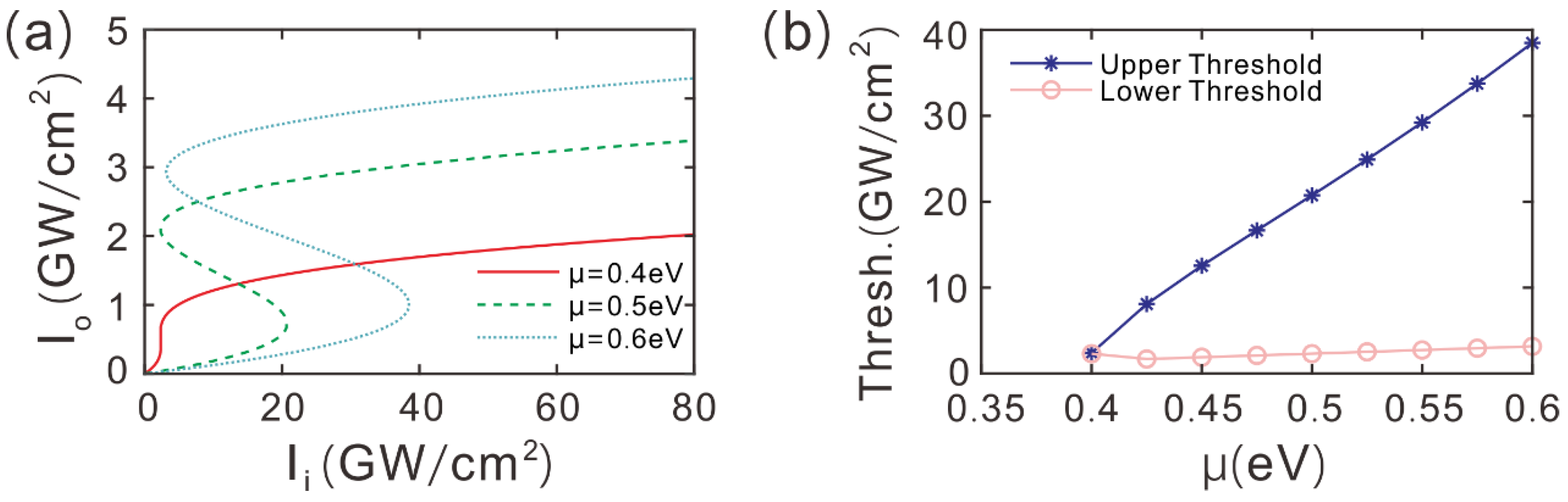
Figure 5a provides the input–output relationship of light intensity. Here,
Te = 100 K, and
λ = 1.56 μm. For the values of
μ = 0.5 and 0.6 eV, we can see that there is an S-shape in each curve (i.e., an OB). For
μ = 0.4 eV, there is not a S-shaped curve segment in the input–output relationship curve; i.e., the bistable relationship is not supported. However, compared with the results in the cases of
μ = 0.5 and 0.6 eV, the values of
Iiu,
Iid, and
Iint increase.
Figure 5b shows that the thresholds of OB depend on the graphene chemical potential for
λ = 1.56 μm. The environment temperature is
Te = 100 K. This graph shows that the bistable action emerges as
μ > 0.4 eV, the OB threshold and threshold interval increase with the increase in the graphene chemical potential. Therefore, the appearance of OB and its threshold parameters can be controlled by the chemical potential.
One can see that the nonlinear conductivity coefficient of graphene is inversely proportional to the chemical potential of graphene from Equation (7). Therefore, the nonlinearity of graphene shrinks as the increase in the potential of graphene. It needs stronger incident light energy to meet the resonant condition for a larger value of graphene chemical potential, which can be utilized to explain why the thresholds of OB increase with the increase in the chemical potential of graphene.
In our previous studies [
1,
3], we used the electric field localization of defect state to strengthen the nonlinear effect of graphene. The threshold parameters can be flexibly adjusted by
μ,
λ, and
θ. Otherwise, some studies have been done on OB in PC heterostructure based on topological edge states [
17,
20,
23]; the hysteresis behavior and OB threshold are also adjusted by the Fermi energy of graphene, as well as the wavelength and angle of the incident beam. The dielectric constant of conventional dielectrics and the conductivity of graphene are functions of temperature, but the performance of OB controlled by temperature is not obviously dependent. For our proposed project, the PC includes the following components: high-temperature superconductor and semiconductor materials. The results show that the proposed composite structure can have the same photonic band gap characteristics as the periodic structure. The dielectric constant of these materials varies with the environment temperature, which means that the threshold and threshold interval of OB can be flexibly controlled by environment temperature, rather than just through graphene and incident beam. The OB is further applied to the temperature control switch. The upper and lower thresholds of OB correspond to the opening and closing thresholds of the temperature control switch, which is the feature of this paper.
The photonic crystal can support the defect mode as a defect is embedded at the center of the structure. The local electric field of the defect mode is the strongest in the central position, so the optical nonlinearity could be greatly enhanced under considering the three-order nonlinear effect of the defect. Optical bistability and solitons were further achieved in the defect photonic crystal [
43,
44]. The threshold of optical bistability can be modulated through the chemical potential of graphene which is embedded at the interfaces of the defect [
45]. However, Zheng et al. neglected the nonlinearity of graphene though three-order nonlinear coefficient is an order of magnitude larger than that of the conventional dielectric, such as SiO
2 [
45,
46]. Otherwise, the optical soliton is a transversal distributed mode, while the defect mode is longitudinal. The optical bistability therefore results from the localization of longitudinal electric field. We here realize the optical bistability based on the nonlinearity of graphene in defect photonic crystals. Of which graphene is embedded at the site where the local electric field is the strongest in the whole system. Consequently, the nonlinearity of graphene has been greatly enhanced, and low-threshold bistability is realized.


 ,
, 


