
Influence of Thermal Treatment on the Cross-Sectional Properties of Aerosol-Deposited Pb(Mg1/3Nb2/3)O3−PbTiO3 Thick Films
 , , and
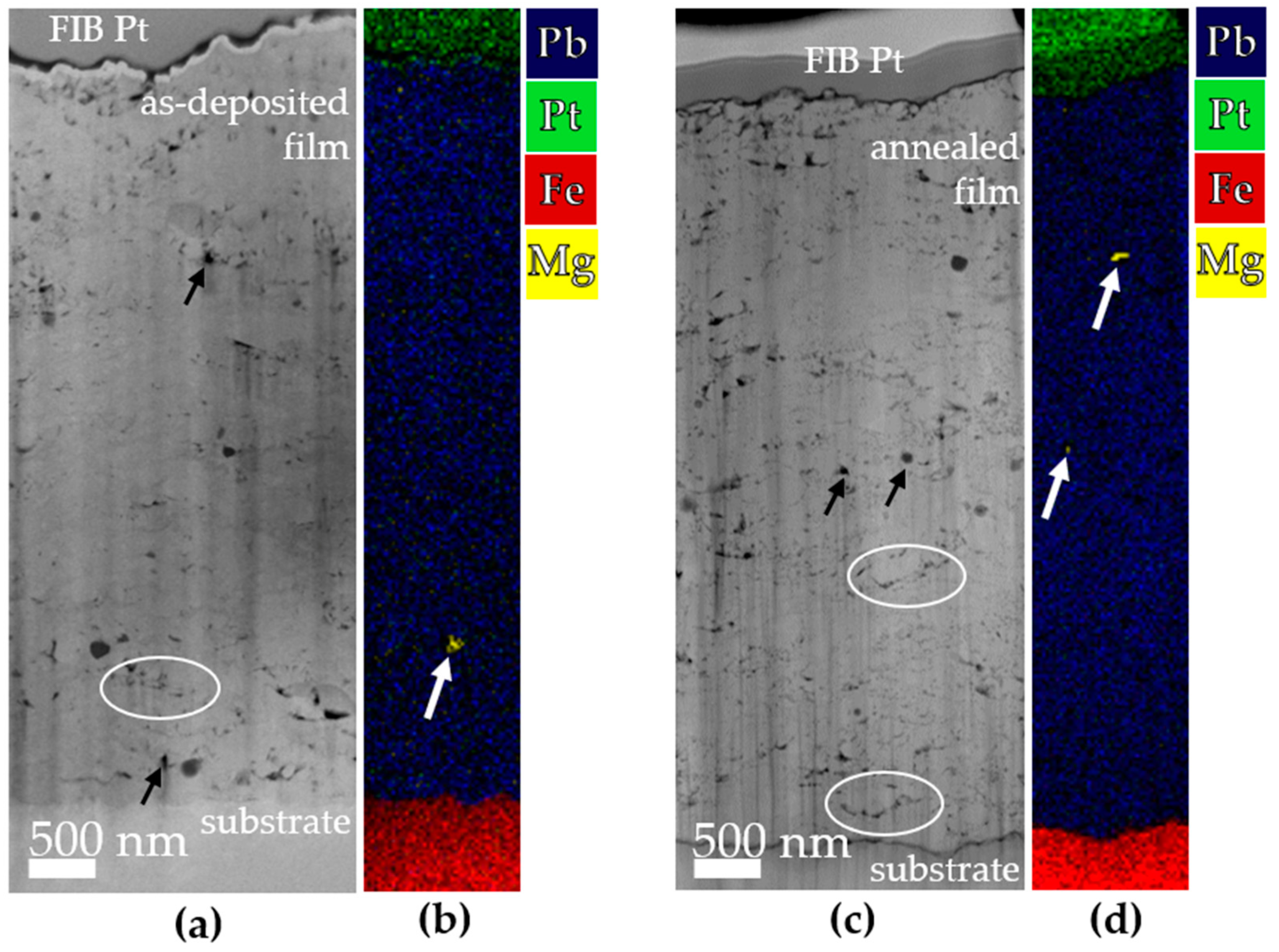
Abstract
:1. Introduction
2. Materials and Methods
3. Results and Discussion
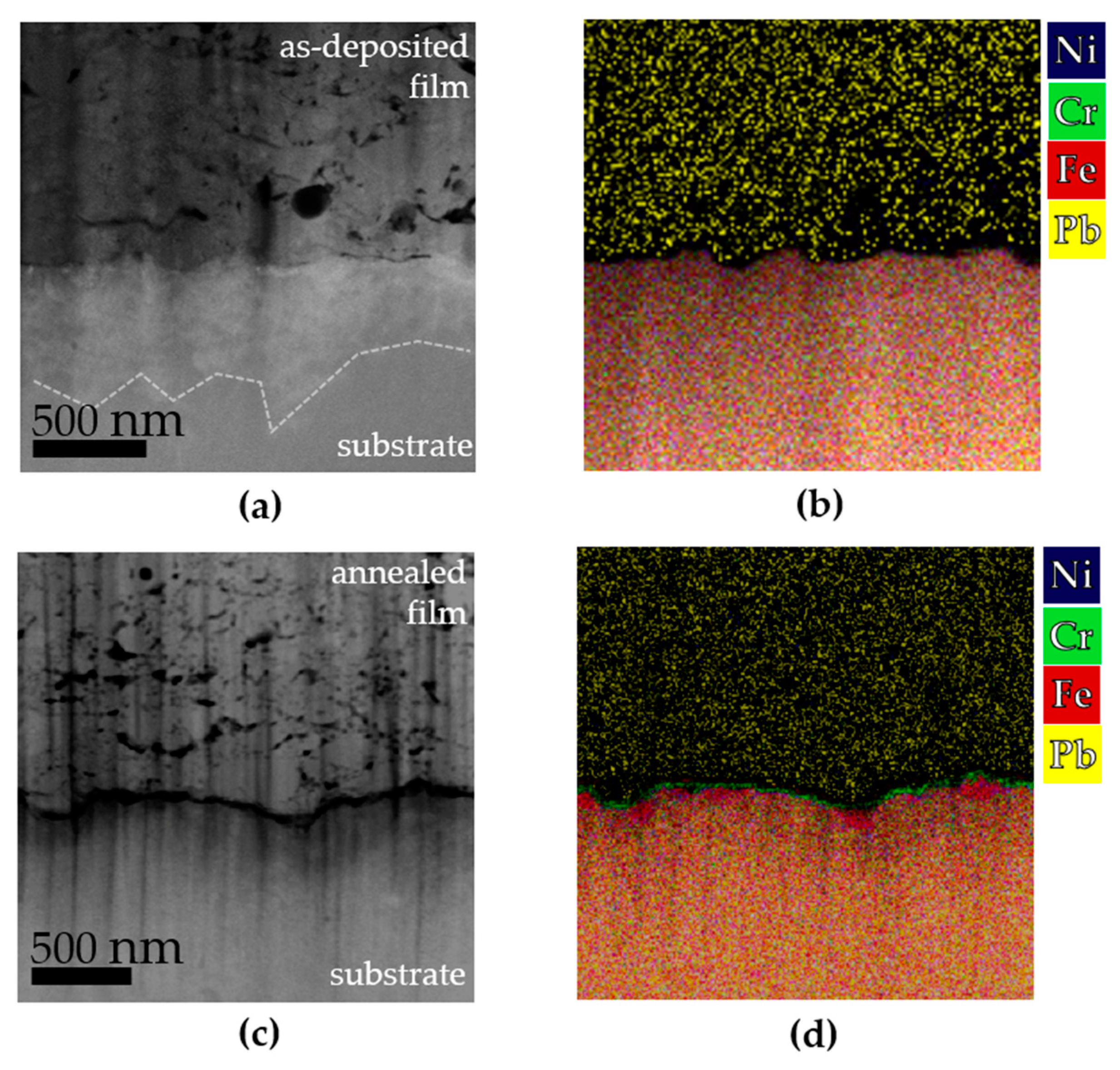
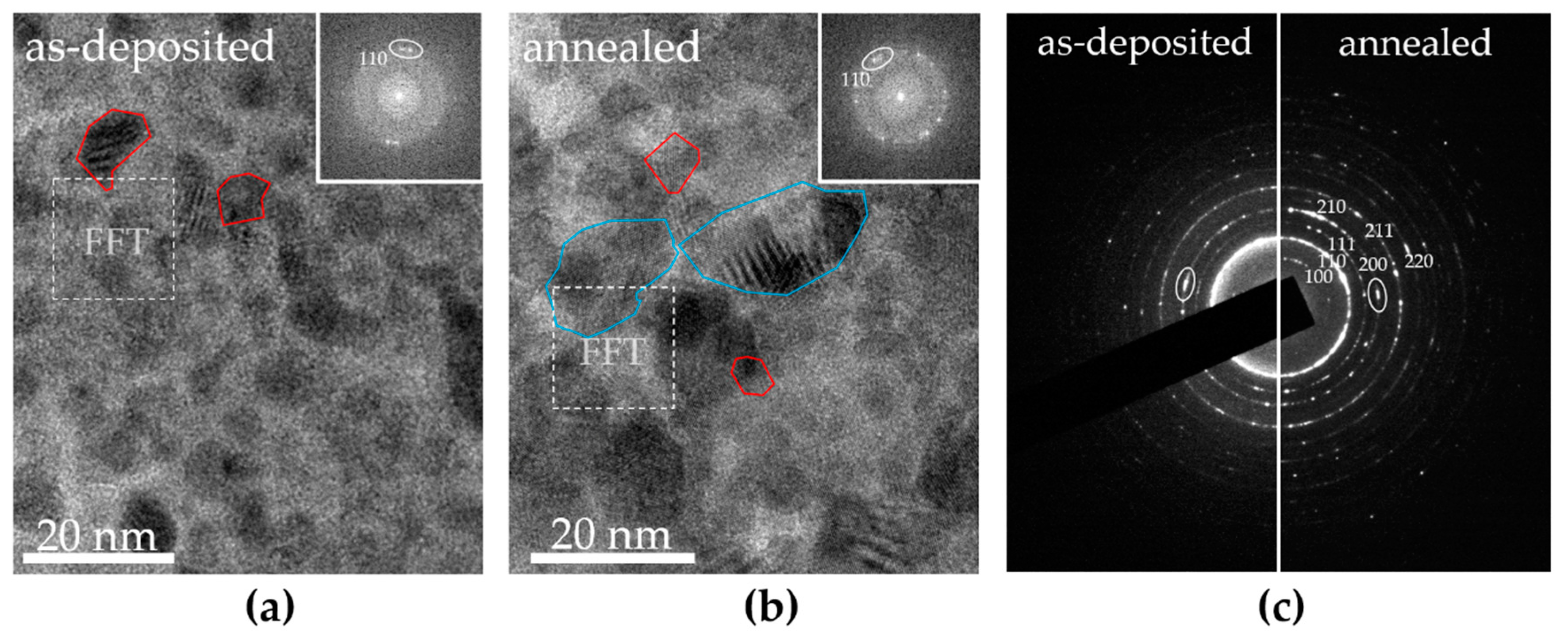
3.1. Microstructure and Chemical Composition
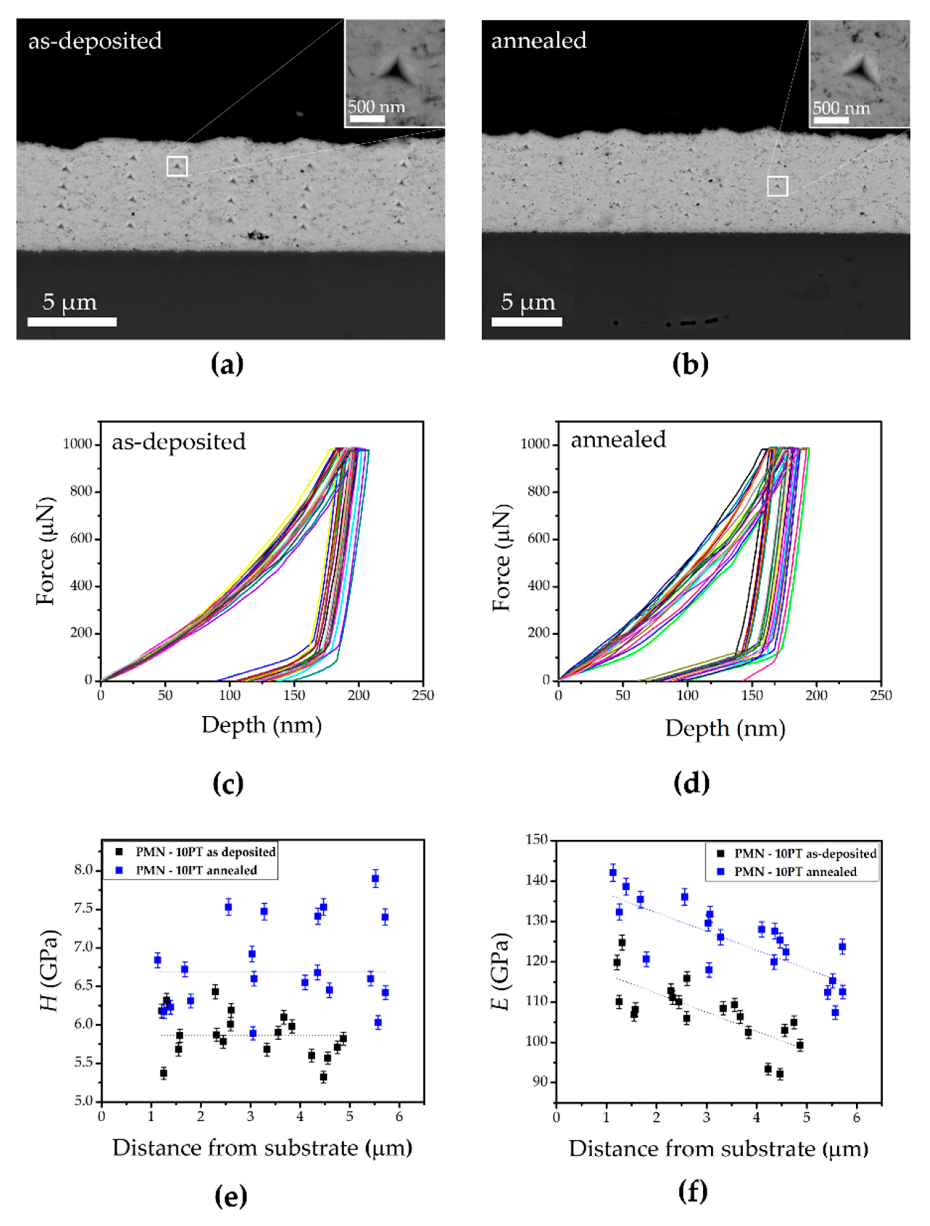
3.2. Mechanical Behavior
4. Conclusions
Supplementary Materials
Author Contributions
Funding
Data Availability Statement
Acknowledgments
Conflicts of Interest
References
- Hanft, D.; Exner, J.; Schubert, M.; Stöcker, T.; Fuierer, P.; Moos, R. An Overview of the Aerosol Deposition Method: Process Fundamentals and New Trends in Materials Applications. J. Ceram. Sci. Technol. 2015, 6, 147–181. [Google Scholar] [CrossRef]
- Schubert, M.; Hanft, D.; Nazarenus, T.; Exner, J.; Nieke, P.; Glosse, P.; Leupold, N.; Kita, J.; Moos, R. Powder Aerosol Deposition Method—Novel Applications in the Field of Sensing and Energy Technology. Funct. Mater. Lett. 2019, 12, 1930005. [Google Scholar] [CrossRef] [Green Version]
- Akedo, J. Room Temperature Impact Consolidation (RTIC) of Fine Ceramic Powder by Aerosol Deposition Method and Applications to Microdevices. J. Therm. Spray Technol. 2008, 17, 181–198. [Google Scholar] [CrossRef]
- Saunders, R.; Johnson, S.D.; Schwer, D.; Patterson, E.A.; Ryou, H.; Gorzkowski, E.P. A Self-Consistent Scheme for Understanding Particle Impact and Adhesion in the Aerosol Deposition Process. J. Therm. Spray Technol. 2021, 30, 523–541. [Google Scholar] [CrossRef]
- Akedo, J.; Lebedev, M. Piezoelectric Properties and Poling Effect of Pb(Zr, Ti)O3 Thick Films Prepared for Microactuators by Aerosol Deposition. Appl. Phys. Lett. 2000, 77, 1710–1712. [Google Scholar] [CrossRef]
- Akedo, J.; Lebedev, M. Microstructure and Electrical Properties of Lead Zirconate Titanate (Pb(Zr52/Ti48)O3) Thick Films Deposited by Aerosol Deposition Method. Jpn. J. Appl. Phys. 1999, 38, 5397–5401. [Google Scholar] [CrossRef]
- Kim, H.K.; Oh, J.M.; Kim, S.I.; Kim, H.J.; Lee, C.W.; Nam, S.M. Relation between Electrical Properties of Aerosol-Deposited BaTiO3 Thin Films and Their Mechanical Hardness Measured by Nano-Indentation. Nanoscale Res. Lett. 2012, 7, 1–16. [Google Scholar] [CrossRef] [Green Version]
- Khansur, N.H.; Eckstein, U.; Li, Y.; Hall, D.A.; Kaschta, J.; Webber, K.G. Revealing the Effects of Aerosol Deposition on the Substrate-Film Interface Using NaCl Coating. J. Am. Ceram. Soc. 2019, 102, 5763–5771. [Google Scholar] [CrossRef]
- Khansur, N.H.; Eckstein, U.; Benker, L.; Deisinger, U.; Merle, B.; Webber, K.G. Room Temperature Deposition of Functional Ceramic Films on Low-Cost Metal Substrate. Ceram. Int. 2018, 44, 16295–16301. [Google Scholar] [CrossRef]
- Sadl, M.; Condurache, O.; Bencan, A.; Dragomir, M.; Prah, U.; Malic, B.; Deluca, M.; Eckstein, U.; Hausmann, D.; Khansur, N.H.; et al. Energy-Storage-Efficient 0.9Pb(Mg1/3Nb2/3)O3–0.1PbTiO3 Thick Films Integrated Directly onto Stainless Steel. Acta Mater. 2021, 221, 117403. [Google Scholar] [CrossRef]
- Sadl, M.; Nadaud, K.; Bah, M.; Levassort, F.; Eckstein, U.; Khansur, N.H.; Webber, K.G.; Ursic, H. Multifunctional Energy Storage and Piezoelectric Properties of 0.65Pb(Mg1/3Nb2/3)O3-0.35PbTiO3 thick Films on Stainless-Steel Substrates. J. Phys. Energy 2022, 4, 024004. [Google Scholar] [CrossRef]
- Zhuo, F.; Eckstein, U.R.; Khansur, N.H.; Dietz, C.; Urushihara, D.; Asaka, T.; Kakimoto, K.I.; Webber, K.G.; Fang, X.; Rödel, J. Temperature-Induced Changes of the Electrical and Mechanical Properties of Aerosol-Deposited BaTiO3 Thick Films for Energy Storage Applications. J. Am. Ceram. Soc. 2022, 105, 4108–4121. [Google Scholar] [CrossRef]
- Eckstein, U.; Exner, J.; Bencan Golob, A.; Ziberna, K.; Drazic, G.; Ursic, H.; Wittkämper, H.; Papp, C.; Kita, J.; Moos, R.; et al. Temperature-Dependent Dielectric Anomalies in Powder Aerosol Deposited Ferroelectric Ceramic Films. J. Mater. 2022, 8, 1239–1250. [Google Scholar] [CrossRef]
- Suzuki, M.; Akedo, J. Temperature Dependence of Dielectric Properties of Barium Titanate Ceramic Films Prepared by Aerosol Deposition Method. Jpn. J. Appl. Phys. 2010, 49, 09MA10. [Google Scholar] [CrossRef]
- Khansur, N.H.; Eckstein, U.; Uršič, H.; Sadl, M.; Brehl, M.; Martin, A.; Riess, K.; de Ligny, D.; Webber, K.G. Enhanced Electromechanical Response and Thermal Stability of 0.93(Na1/2Bi1/2)TiO3-0.07BaTiO3 Through Aerosol Deposition of Base Metal Electrodes. Adv. Mater. Interfaces 2021, 8, 2100309. [Google Scholar] [CrossRef]
- Sadl, M.; Lebar, A.; Valentincic, J.; Ursic, H. Flexible Energy-Storage Ceramic Thick-Film Structures with High Flexural Fatigue Endurance. ACS Appl. Energy Mater. 2022, 5, 6896–6902. [Google Scholar] [CrossRef]
- Maruyama, K.; Kawakami, Y.; Narita, F. Young’s Modulus and Ferroelectric Property of BaTiO3 Films Formed by Aerosol Deposition in Consideration of Residual Stress and Film Thickness. Jpn. J. Appl. Phys. 2022, 61, SN1011. [Google Scholar] [CrossRef]
- Nadaud, K.; Sadl, M.; Bah, M.; Levassort, F.; Ursic, H. Effect of Thermal Annealing on Dielectric and Ferroelectric Properties of Aerosol-Deposited 0.65Pb(Mg1/3Nb2/3)O3-0.35PbTiO3 thick Films. Appl. Phys. Lett. 2022, 120, 112902. [Google Scholar] [CrossRef]
- Ryu, J.; Choi, J.J.; Hahn, B.D.; Park, D.S.; Yoon, W.H. Ferroelectric and Piezoelectric Properties of 0.948(K0.5Na0.5)NbO3−0.052LiSbO3 Lead-Free Piezoelectric Thick Film by Aerosol Deposition. Appl. Phys. Lett. 2008, 92, 2006–2009. [Google Scholar] [CrossRef]
- Hoshina, T.; Furuta, T.; Kigoshi, Y.; Hatta, S.; Horiuchi, N.; Takeda, H.; Tsurumi, T. Size Effect of Nanograined BaTiO3 Ceramics Fabricated by Aerosol Deposition Method. Jpn. J. Appl. Phys. 2010, 49, 03MC02. [Google Scholar] [CrossRef]
- Khansur, N.H.; Eckstein, U.; Riess, K.; Martin, A.; Drnec, J.; Deisinger, U.; Webber, K.G. Synchrotron X-ray Microdiffraction Study of Residual Stresses in BaTiO3 Films Deposited at Room Temperature by Aerosol Deposition. Scr. Mater. 2018, 157, 86–89. [Google Scholar] [CrossRef]
- Sadl, M.; Tomc, U.; Prah, U.; Ursic, H. Protective Alumina Coatings Prepared by Aerosol Deposition on Magnetocaloric Gadolinium Elements. Inf. MIDEM 2019, 49, 177–182. [Google Scholar] [CrossRef]
- ImageJ. Available online: https://imagej.net/ij/ (accessed on 27 December 2022).
- Oliver, W.C.; Phaar, G.M. An Improvved Techniques for Determining Hardness and Elastic Modulus Using Using Load and Dispacement Sensing Indentation Experiments. J. Mater. Res. 1992, 7, 1564–1583. [Google Scholar] [CrossRef]
- Catalan, G.; Corbett, M.H.; Bowman, R.M.; Gregg, J.M. Effect of Thermal Expansion Mismatch on the Dielectric Peak Temperature of Thin Film Relaxors. J. Appl. Phys. 2002, 91, 2295–2301. [Google Scholar] [CrossRef]
- Uršič, H.; Vrabelj, M.; Otoničar, M.; Furlanović, L.; Rožič, B.; Kutnjak, Z.; Bobnar, V.; Malič, B. Influence of Synthesis-Related Microstructural Features on the Electrocaloric Effect for 0.9Pb(Mg1/3Nb2/3)O3–0.1PbTiO3 Ceramics. Crystals 2021, 11, 372. [Google Scholar] [CrossRef]
- Stainless Steel—Grade 304 (UNS S30400). Available online: https://www.azom.com/properties.aspx?ArticleID=965 (accessed on 13 January 2023).
- Walls, M.G.; Chaudhri, M.M.; Tang, T.B. Stm Profilometry of Low-Load Vickers Indentations in a Silicon Crystal. J. Phys. D Appl. Phys. 1992, 25, 500–507. [Google Scholar] [CrossRef]
- Devaraj, A.; Barton, D.J.; Li, C.H.; Lambeets, S.V.; Liu, T.; Battu, A.; Vaithiyalingam, S.; Thevuthasan, S.; Yang, F.; Guo, J.; et al. Visualizing the Nanoscale Oxygen and Cation Transport Mechanisms during the Early Stages of Oxidation of Fe–Cr–Ni Alloy Using In Situ Atom Probe Tomography. Adv. Mater. Interfaces 2022, 9, 2200134. [Google Scholar] [CrossRef]
- Navickas, E.; Huber, T.M.; Chen, Y.; Hetaba, W.; Holzlechner, G.; Rupp, G.; Stöger-Pollach, M.; Friedbacher, G.; Hutter, H.; Yildiz, B.; et al. Fast Oxygen Exchange and Diffusion Kinetics of Grain Boundaries in Sr-Doped LaMnO3 Thin Films. Phys. Chem. Chem. Phys. 2015, 17, 7659–7669. [Google Scholar] [CrossRef] [Green Version]
- Daneshian, B.; Gärtner, F.; Assadi, H.; Vidaller, M.V.; Höche, D.; Klassen, T. Features of Ceramic Nanoparticle Deformation in Aerosol Deposition Explored by Molecular Dynamics Simulation. Surf. Coat. Technol. 2022, 429, 127886. [Google Scholar] [CrossRef]
- Porz, L.; Klomp, A.J.; Fang, X.; Li, N.; Yildirim, C.; Detlefs, C.; Bruder, E.; Höfling, M.; Rheinheimer, W.; Patterson, E.A.; et al. Dislocation-Toughened Ceramics. Mater. Horiz. 2021, 8, 1528–1537. [Google Scholar] [CrossRef]
- Zak, S.; Trost, C.O.W.; Kreiml, P.; Cordill, M.J. Accurate Measurement of Thin Film Mechanical Properties Using Nanoindentation. J. Mater. Res. 2022, 37, 1373–1389. [Google Scholar] [CrossRef]


Disclaimer/Publisher’s Note: The statements, opinions and data contained in all publications are solely those of the individual author(s) and contributor(s) and not of MDPI and/or the editor(s). MDPI and/or the editor(s) disclaim responsibility for any injury to people or property resulting from any ideas, methods, instructions or products referred to in the content. |
© 2023 by the authors. Licensee MDPI, Basel, Switzerland. This article is an open access article distributed under the terms and conditions of the Creative Commons Attribution (CC BY) license (https://creativecommons.org/licenses/by/4.0/).
Share and Cite
Žiberna, K.; Šadl, M.; Drnovšek, A.; Dražić, G.; Uršič, H.; Benčan, A. Influence of Thermal Treatment on the Cross-Sectional Properties of Aerosol-Deposited Pb(Mg1/3Nb2/3)O3−PbTiO3 Thick Films. Crystals 2023, 13, 536. https://doi.org/10.3390/cryst13030536
Žiberna K, Šadl M, Drnovšek A, Dražić G, Uršič H, Benčan A. Influence of Thermal Treatment on the Cross-Sectional Properties of Aerosol-Deposited Pb(Mg1/3Nb2/3)O3−PbTiO3 Thick Films. Crystals. 2023; 13(3):536. https://doi.org/10.3390/cryst13030536
Chicago/Turabian StyleŽiberna, Katarina, Matej Šadl, Aljaž Drnovšek, Goran Dražić, Hana Uršič, and Andreja Benčan. 2023. "Influence of Thermal Treatment on the Cross-Sectional Properties of Aerosol-Deposited Pb(Mg1/3Nb2/3)O3−PbTiO3 Thick Films" Crystals 13, no. 3: 536. https://doi.org/10.3390/cryst13030536