Article

Three-Dimensional MoS2 Nanosheet Structures: CVD Synthesis, Characterization, and Electrical Properties

1
FG-Nanotechnologie, Institut für Mikro-und Nanoelektronik, Institut für Mikro-und Nanotechnologien MacroNano®, Institut für Werkstofftechnik, TU Ilmenau, Postfach 100565, 98684 Ilmenau, Germany
2
FG Technische Physik I, Institut für Physik, Institut für Mikro-und Nanotechnologien MacroNano®, Technische Universität Ilmenau, 98684 Ilmenau, Germany
3
FG-Werkstoffe der Elektrotechnik, Institut für Werkstofftechnik, Institut für Mikro- und Nanotechnologien MacroNano®, TU Ilmenau, Gustav-Kirchhoff-Straße 5, 98693 Ilmenau, Germany
*
Author to whom correspondence should be addressed.
Crystals 2023, 13(3), 448; https://doi.org/10.3390/cryst13030448
Submission received: 11 February 2023 / Revised: 28 February 2023 / Accepted: 2 March 2023 / Published: 4 March 2023
(This article belongs to the Special Issue Recent Developments of Inorganic Crystalline Materials)

Abstract

:
The proposed study demonstrates a single-step CVD method for synthesizing three-dimensional vertical MoS2 nanosheets. The postulated synthesizing approach employs a temperature ramp with a continuous N2 gas flow during the deposition process. The distinctive signals of MoS2 were revealed via Raman spectroscopy study, and the substantial frequency difference in the characteristic signals supported the bulk nature of the synthesized material. Additionally, XRD measurements sustained the material’s crystallinity and its 2H-MoS2 nature. The FIB cross-sectional analysis provided information on the origin and evolution of the vertical MoS2 structures and their growth mechanisms. The strain energy produced by the compression between MoS2 islands is assumed to primarily drive the formation of vertical MoS2 nanosheets. In addition, vertical MoS2 structures that emerge from micro fissures (cracks) on individual MoS2 islands were observed and examined. For the evaluation of electrical properties, field-effect transistor structures were fabricated on the synthesized material employing standard semiconductor technology. The lateral back-gated field-effect transistors fabricated on the synthesized material showed an n-type behavior with field-effect mobility of 1.46 cm2 V−1 s−1 and an estimated carrier concentration of 4.5 × 1012 cm−2. Furthermore, the effects of a back-gate voltage bias and channel dimensions on the hysteresis effect of FET devices were investigated and quantified.

1. Introduction

Transition metal dichalcogenides (TMDs) have received much attention in advanced material science and technology due to their unique material properties. Among this material class, molybdenum disulfide (MoS2) has been extensively used in many device applications [1,2]. Moreover, its unique semiconductor properties have gained much recognition among 2D materials for various promising applications. As a result, many bottom-up approaches have been developed to synthesize large-scale MoS2, including sulfurization of the Mo layer [3,4,5,6,7] and chemical vapor deposition (CVD) [8,9,10,11,12,13]. However, among the numerous vapor phase reactions, researchers mainly emphasized horizontally grown 2D materials on planar substrates rather than the vertical formation of MoS2 structures.
Nevertheless, some research has recently been conducted on the vertical formation of MoS2 nanostructures [14,15,16,17]. In addition, several studies have been made to analyze the growth mechanism of this vertical formation of MoS2 [14,17]. In vertical MoS2, the physical properties may vary due to its growth direction, making it a promising candidate for diverse applications. For example, the high aspect ratio, presence of dangling bonds, and extensively exposed edges with a high absorption rate of vertical MoS2 nanosheets show outstanding gas-sensing properties [18,19]. Furthermore, vertically exposed structures with chemically active sites and catalytically active zones make them suitable for photocatalytic, hydrogen evolution reactions (HER) and many other promising applications [16,20,21].
Additionally, the vertically formed MoS2 nanoflakes exhibit excellent optical absorption with enhanced photoresponsivity and interlayer transport, making them a highly efficient material for photodetection, optoelectronic applications [22,23], and field emission applications [24]. However, the studies based on the formation and electrical properties of the vertical MoS2 structures have not received much attention in research. Although numerous investigations on horizontal MoS2-based planar devices with multi-terminal designs have been conducted, understanding of the structural development and electrical characterization of devices based on vertical MoS2 nanosheets remains sporadic.
This study presents the development and investigation of a reliable, single-step CVD method for synthesizing three-dimensional (3D) vertical MoS2 nanosheets. The developed synthesizing approach uses the vapor phase reaction of solid precursors with a ramping temperature and a constant N2 gas flow for the vertical growth of MoS2 nanosheets. In addition, the time-dependent growth morphologies of MoS2 were analyzed using scanning electron microscope (SEM) and focused ion beam (FIB), and the growth mechanism and evolution of the vertical structures was examined. Employing standard semiconductor technology, several lateral backgated field effect transistors were fabricated using the synthesized material. Furthermore, the electrical properties were determined by measuring the FET devices in ambient environment.

2. Materials and Methods

2.1. Growth Method

For the preferential growth of vertical MoS2 thin films, we employed the vapor phase reactions of the precursor materials molybdenum (MoO3) and sulfur (S). The developed process was performed in a 1.2 m long quartz tube with inner and outer diameters of 4.6 and 5 cm, respectively, as shown in Figure S1 (supplementary information). In a typical growth process, silicon substrates (1 × 1 cm) with a 90 nm thick SiO2 layer were initially cleaned in acetone, isopropanol, and a deionized water bath for 10 min, and subsequently dried using nitrogen gas. The substrates were then inserted into the quartz tube and positioned in the center of a single-zone horizontal tube furnace. After that, we placed a ceramic boat containing the precursor MoO3 powder (0.3 mg) (99%, Sigma-Aldrich) in the center of the quartz tube (40 cm from the inlet). The sulfur (S, 0.6 mg) (99% Sigma-Aldrich) source was positioned at a lower temperature position (27 cm upstream from the inlet). The furnace was then purged with 500 sccm of nitrogen for one hour. After purging, the furnace’s temperature was increased to a predetermined level of 850 °C using a linear heating ramp that increased by 28 °C per minute with a flow of 500 sccm of nitrogen gas. The heating ramp was slowed down once 850 °C was reached. The temperatures were monitored using thermocouples. The sulfur was kept at a constant temperature of 240 °C. The growth process was carried out for different growth times that varied from 10 min to 30 min. Finally, a 500 sccm nitrogen flow operating at atmospheric pressure brought the system down to ambient temperature. The temperature–time profile of the whole CVD process is given in Figure S1 (supplementary information).

2.2. Characterization of Synthesized 3D Verical MoS2 Nanosheet

The surface morphology and topographical details of the vertical MoS2 nanosheets were analyzed using optical microscopy and SEM. A cross-sectional study also has been performed with a FIB device (Zeiss Auriga 60 dual beam) to analyze the inner morphology of the vertical structures. Before cutting, protective carbon and platinum layers were deposited sequentially via an electron beam. A gallium ion beam was used to realize the cuts. Furthermore, we investigated the material properties with Raman spectroscopy and X-ray diffraction (XRD). The Raman spectra were obtained using a WiTec Alpha 300R with 532 nm excitation. X-ray diffraction (XRD) was performed using a Siemens D5000 with a copper anode (radiation: 0.15406 nm for Kα1 (Bragg—Brentano mode)).

2.3. Device Fabrication

The devices were fabricated using a maskless aligner (MLA) photolithography tool from the Heidelberg Instrument. First, the CVD-grown MoS2 samples were cleaned, pre-baked, and coated with an adhesion promoter, hexamethyldisilazane (HMDS). Later, the samples were spin-coated at 4000 rpm with a positive resist (AZ1505). After the material was structured by image inversion using MLA, the exposed structures were developed in AZ 351-B for 30 s. Subsequently, the samples were etched using Cl2 and O2 plasma for 1 min, and the resist was removed by acetone. After etching, the samples were again coated with HMDS and later spin-coated with another positive resist (AZ 1518) at 4000 rpm to pattern the metal contacts. Then, the patterned resist was developed in AZ 315-B and metalized with Titanium (Ti-10 nm) and gold (Au-80 nm) using electron beam evaporation. The metal deposited on the resist was removed in a lift-off step in dimethyl sulfoxide (DMSO) for 30 min.

3. Results and Discussion

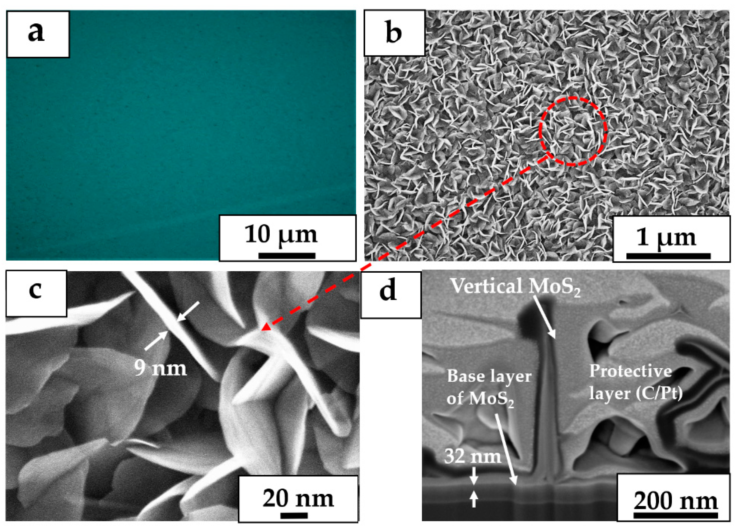
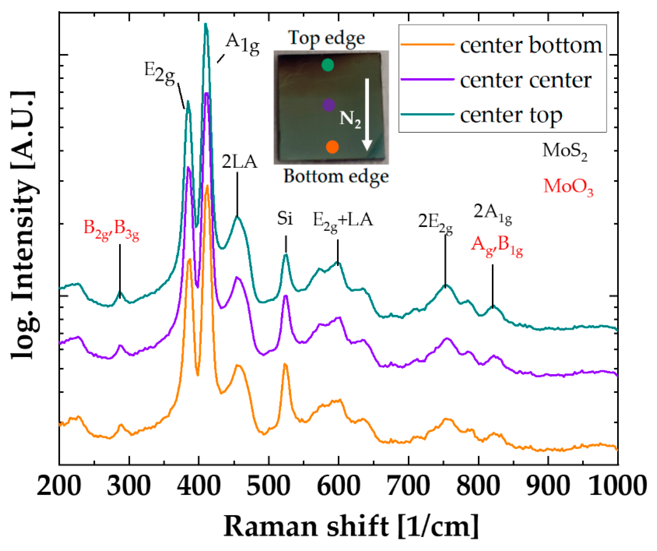
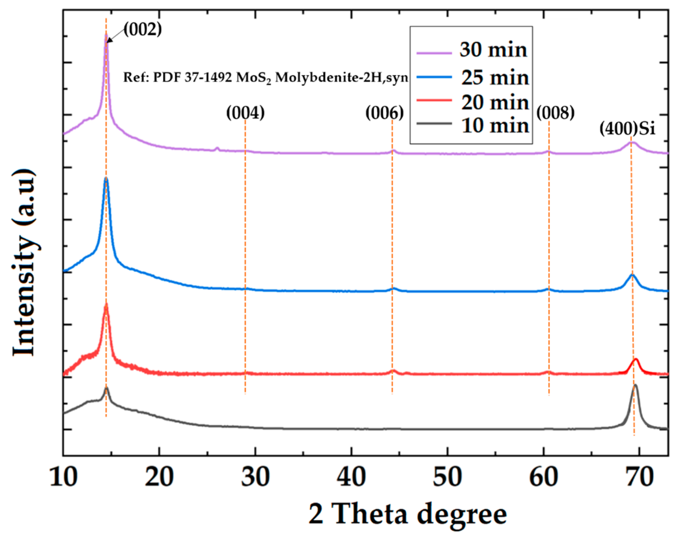
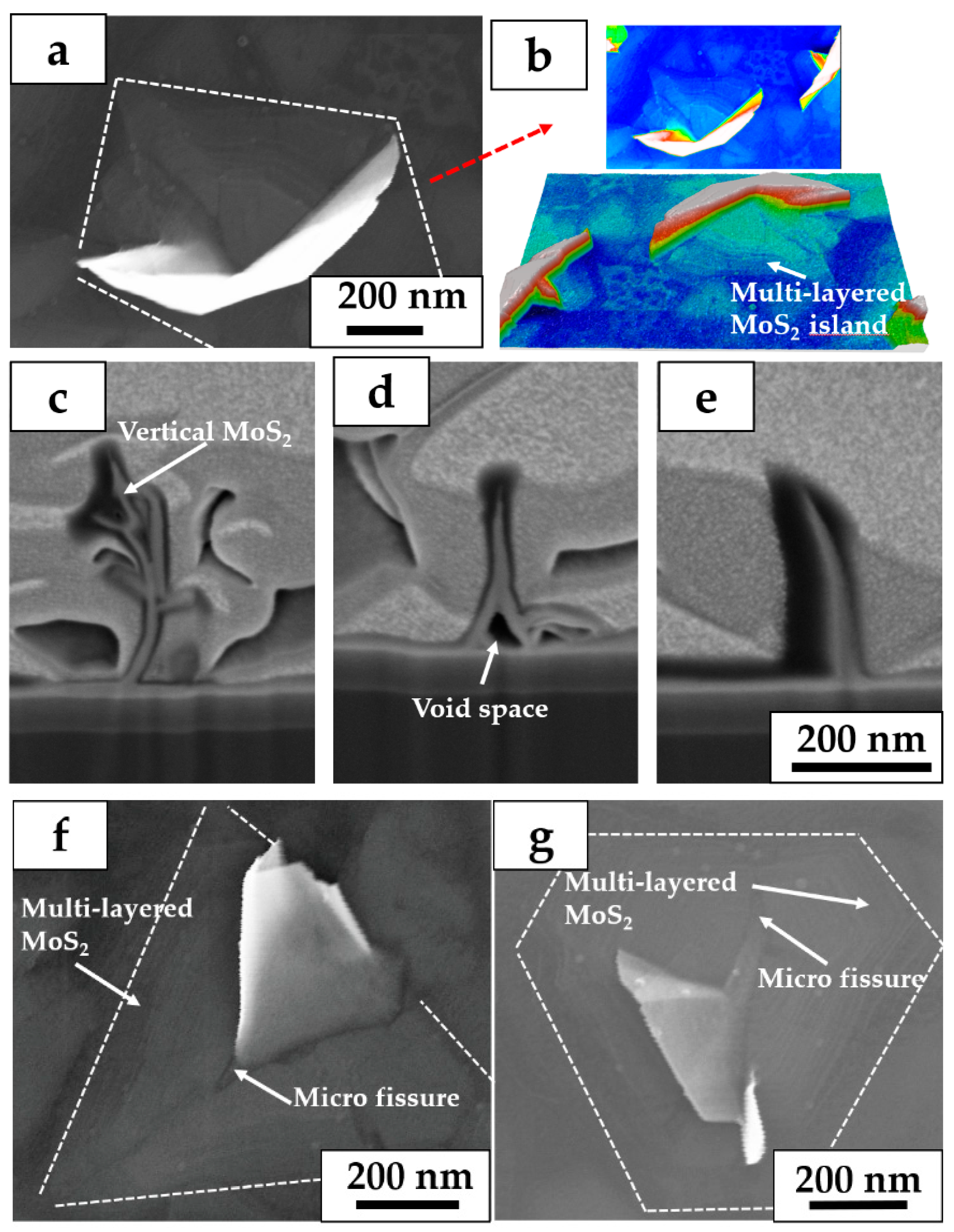
3.1. Formation and Characterization of the Three-Dimensional MoS2 Nanosheet

A typical optical micrograph image obtained from the MoS2 nanosheet sample surface is shown in Figure 1a. The homogeneous interference color demonstrates a homogeneous deposition on the substrate. Figure 1b,c show SEM images. In them, a three-dimensional (3D) MoS2 nanosheet structure can be observed.
The MoS2 has randomly grown vertically from the substrate surface, forming three-dimensional vertical nanostructures representing a quasiperiodic modulation of the material surface. Each nanosheet has a flower petal-like shape with sub-20 nm dimension thin edges, as illustrated in Figure 1c. Furthermore, these vertical structures have nano-sized edge sites with multiple grain boundaries. On the substrates, these nano platelets are grown dominantly in the vertical direction, exposing their edge sites rather than their basal planes. Moreover, these structures often possess a high aspect ratio with more edge sites suitable for many applications.
A cross-sectional examination was conducted to better understand the early stages of the vertical MoS2 formation. The cross-section samples were prepared using focused ion beam (FIB) technology. The general morphology of vertically free-standing MoS2 nanosheets grown on a SiO2/Si substrate can be observed in the cross-section FIB picture shown in Figure 1d. Most of the vertical structures are oriented perpendicular to the substrate surface. The basal plane of MoS2 is a bulk layer and has a height of 32 nm. The bulk layer is buckled. The buckling is highlighted in Figure S2 with arrows. The buckling is evidence of compressive stress in the deposited polycrystalline 2H-MoS2 layer. Each of these vertical structures possesses a size up to 1 µm and they are formed at the coalescence point of two misoriented MoS2 flakes. Additionally, the thickness of the MoS2 nanosheet is not constant along the vertical nanosheet height. Instead, it has a tapered morphology with a larger basal size with decreasing size towards the end. Detailed morphological attributes of these features are given in Figure S2. It is worth noting that these vertical features have different dimensions and grow randomly upwards with varying thicknesses. Furthermore, the basal plane of the vertical structures has a tetrahedral shape. This tetrahedral layer is a three-dimensional bulk layer of MoS2, as will be discussed later.
The material properties of the vertical MoS2 nanosheet layers were further investigated using X-ray diffraction analysis and Raman spectroscopy measurements. Raman measurements were performed at room temperature under ambient conditions and unpolarized detection. Figure 2 is the corresponding Raman spectrum obtained from the material surface.
The Raman measurements were carried out on the sample surface at three different places. The insets in Figure 2 show the positions where the Raman spectra were obtained. Each spectrum color corresponds to the color assigned to the respective circle shown in the measurement area of the inset in Figure 2. The two dominant Raman modes of MoS2 are revealed by the Raman spectra, which are the in-plane (E12g) and the out-of-plane (A1g) vibrations of the sulfur atoms at 382.5 and 409.0 cm−1, respectively [25]. The study reveals further corresponding Raman peaks of MoS2 attributable to the following two phonon modes such as 2LA (M) at 454 cm−1, [25,26,27,28]; E2g + LA at 600 cm−1; 2E2g at 764 cm−1; and 2A1g at 820 cm−1. As shown in the insets in Figure 2, the top edge is near to the precursor and the bottom edge is facing the outlet of the furnace. The flow direction of N2 is shown with an arrow mark pointing towards the outlet. The Raman measurements obtained from three points show a variation in the intensities of the E12g and A1g modes. This variation can reveal different attributes such as crystallinity, thickness, and defect density of the deposited material [14,29,30]. The intensities of the E12g and A1g peaks are decreasing from the top edge to the bottom edge of the sample. The sample surface near to the precursor has a higher thickness of MoS2 deposition as compared to the other end and a higher defect density of exposed edges of the vertical structures [29,30]. Moreover, most of the peak shapes remain unchanged without any significant peak shift, providing the stable crystal morphology of the MoS2 sand flower-like structures at different positions of the sample. Furthermore, we could not observe any additional peaks at different measurement positions of the sample surface. The wavenumber difference Δ between the E2g and A1g Raman modes is 25 cm−1, confirming the bulk nature of the material [28,30,31]. A weak Raman signal of MoO3 is visible, which can be attributed to partial oxidation at growth or after exposure to air [32].
The X-ray diffraction spectra measured in Bragg−Brentano configuration from the synthesized MoS2 at different deposition times is shown in Figure 3. Here, for each deposition time, the diffraction peak at 14.4° can be attributed to the 2H-MoS2 structure, which corresponds to (002) crystal planes in 2H-MoS2 [33] that are orientated along its c-axis [33,34]. The corresponding higher-order diffraction peaks (004), (006), and (008) are given at their corresponding characteristic designations. While for the deposition time of 10 min we could observe a broader peak with lower intensity at diffraction peak 14.4°, other higher order diffraction peaks are not visible. This might be due to discontinuous and scattered deposition of MoS2. Moreover, the prominent Si (400), compared to other deposition times, further supports the non-uniformity of the MoS2 deposition. However, it is evident that, with an increase in the deposition time, the intensity of the diffraction peaks became prominent and further give significance to the crystallinity of the synthesized MoS2. Unfortunately, diffraction peaks of non-basal planes are not observed. This might be caused by the orientations of these sheets not fulfilling the diffraction.

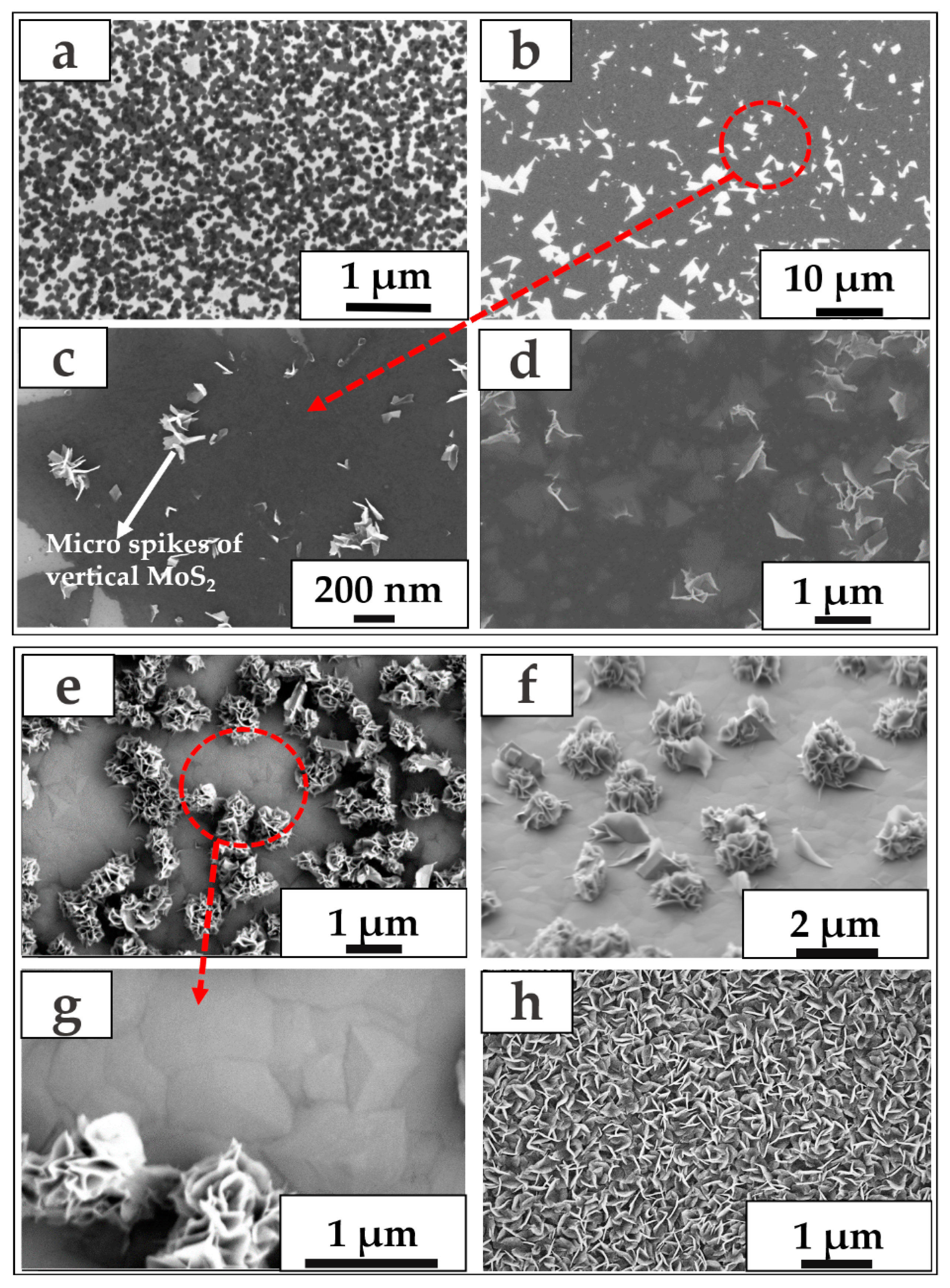
3.2. Evolution and Growth Mechanism of the Three-Dimensional MoS2 Nanosheet

Several samples with varying growth durations were examined to understand the vertical growth mechanism of the MoS2 nanosheets. The growth morphological evolution of the three-dimensional vertical MoS2 nanosheet are summed up in the SEM images in Figure 4. Initially in the growth process, the precursor MoO3 is partially reduced, resulting in the formation of the volatile MoO3-x species [35,36]. The carrier gas transports these under-stoichiometric MoO3-x species to the substrate, where they absorb and diffuse, forming the initial MoS2 nucleation sites. These nucleation sites react with incoming sulfur molecules to form the randomly oriented initial MoS2 grains (flakes) with even-sided triangular shape (Figure 4a). More MoO3−x gets absorbed as the growth time increases, and the nucleation domains enlarge due to the steady supply of reactants [35,37]. Due to the enlarging terrace dimension, secondary nucleation of the next MoS2 layer occurs. This is evidenced by the different grey scale in Figure 4a. In Figure 4b, taken from a sample with a deposition time of 10 min, a random distribution of few-layered MoS2 triangular structures is seen. In this pattern, two types of light grey areas can be noticed: (1) triangular- and (2) non-triangular-like. The triangular-like areas stem from substrate surface uncovered with MoS2. To reveal the nature of the non-triangular feature, higher magnification images were taken. A typical image is shown in Figure 4c.
A closer observation revealed submicron vertical spikes platelets that appeared to have formed at the grain boundaries of the thin layers of MoS2 (see Figure 4c). These the edges cause a higher secondary electron emission. After 15 min of growth time, most triangular structures grow laterally into larger domain sizes and join into a uniform film, as presented in Figure 4d. In addition, it was observed that MoS2 was distributed across the whole substrate surface with several scattered multi-stacked triangular islands (see Figure 4d).
Additional micro spike-like structures also grew along the substrate surface. Then, with the subsequent increase in growth time and constant supply of reactants, more multilayered triangular features developed and started to merge. Eventually, after 25 min of growth, most of the multilayered triangular islands joined and formed a bulk tetrahedral MoS2 thin film, as shown in Figure 4e. Here, the MoS2 thin film exhibits a tetrahedral geometrical shape. The grain boundaries of these structures have a triangular base and a multilayered stepped lateral face. The lateral dimensions of these triangular steps decrease from the bottom to the apex, forming a tetrahedral shape. A magnified SEM image of the tetrahedral structure is shown in Figure 4g. Figure 4f shows the tilted image of those layers with several sand flower-like MoS2 formations. The synthesis of tetrahedral MoS2 thin films was reported previously [9,38,39,40]. This type of structural formation could be referred to as the Stranski−Krastanov-like growth mechanism [41,42,43], which might also stem from Ehrlich−Schwoebel barriers [44].
In Figure 4e, f, a significant number of vertical sand flower-like structures emerged above the bulk layer. Notably, the developed bulk layer formed the base for the vertical MoS2 structures. Many vertical structures were finally formed densely covering the substrate surface after 30 min of growth, as illustrated in Figure 4h. To further clarify the layer transformation of MoS2, Raman measurements were performed on the samples with different growth times. The wavenumber difference between E12g and A1g peaks for various growth times was analyzed and plotted as shown in the supplementary Figure S3. The frequency difference of the prominent peaks of Raman spectra of MoS2 increases with increasing growth time, indicating a transformation of MoS2 structures from a two-dimensional to a three-dimensional structure.
For further elucidation of the formation of vertical MoS2 nanosheets, we have analyzed more plane view and cross-section SEM images at different growth intervals. The so-called extrusion growth model [14] is currently the most acceptable growth mechanism among the numerous growth models for vertically standing MoS2 nanosheets presented in the literature [14,45]. According to this growth model, several multi-layered MoS2 islands are initially developed individually on the substrate surface. Then, once these layers have reached a specific thickness, provided with more supply of reactants and an increase in growth time, these individual islands start to merge to form a thick layer of MoS2. During this process, edge-oriented, vertically standing MoS2 seedlings of the sand flower-like structures are originated. A similar formation of vertical MoS2 seedlings is presented in Figure 5a. As speculated above, the seedlings stemmed from the aggregation zone of different MoS2 islands. A three-dimensional representation of the SEM image shown in Figure 5b confirms the interaction in the aggregation zone between different multilayered MoS2 islands. A comparable formation has already been reported [14,45]. Therefore, FIB cross sections were prepared to gather more information on these MoS2 vertical structures, shown in Figure 5c–e, from different 3D vertical MoS2 structures. The FIB images indicate that the vertical structures are induced by the distorted growth of planar bulk MoS2 layers.
Two types of vertical morphology could generally be observed based on the cross-sectional observations. Figure 5c,e show that most vertical structures originate from the base bulk layer of MoS2, tend to bend or slip with the adjacent MoS2 islands, and grow upwards. Another alternative would be that the vertical structure was formed by converging two separate MoS2 films, creating a void space between them, as shown in Figure 5d. These two inferences provide direct evidence of forming a vertical MoS2 nanosheet consistent with the known growth model. Thus, the formation of vertical standing MoS2 seedlings could be attributed to the compressive force created by developing deformations and strain energy [14,45,46].
However, based on our experimental results, we could also observe a seedling of vertical MoS2 structures that originates from the micro fissures (cracks) appearing on individual MoS2 islands, as shown in Figure 5f,g. Furthermore, it could be observed that the vertically standing MoS2 seedlings appear from the micro fissures on separate MoS2 islands with different geometrical features. Therefore, we believe that these self-formative micro cracks arise during the growth and vertical nanosheets extrude from these cracks due to the strain energy inside the cracks.

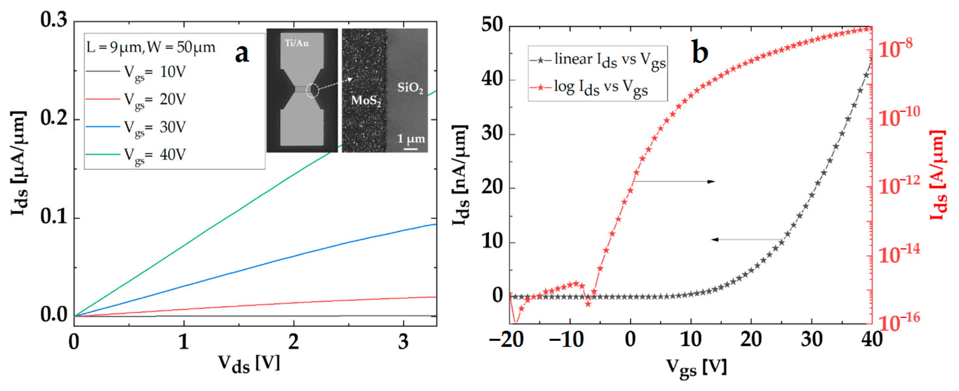
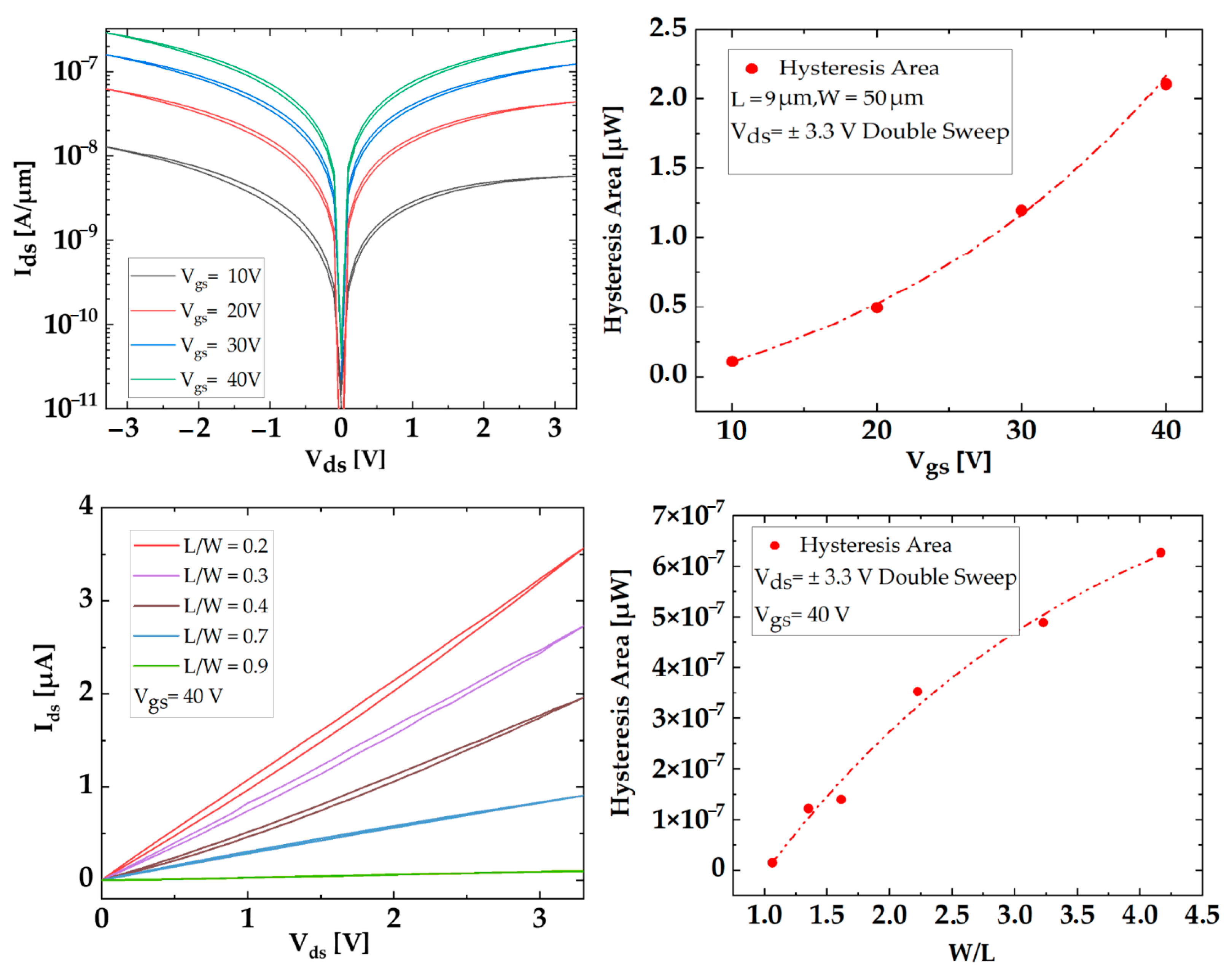
3.3. Electrical Performance of FET Devices on the 3D Vertical MoS2 Nanosheet

We performed electrical tests on fabricated field-effect transistor (FET) devices to analyze the electrical properties of the synthesized material. The measured characteristics of devices fabricated on vertical MoS2 nanosheets are illustrated in Figure 6. The insets in Figure 6a are the SEM picture of the fabricated lateral device. The electrical measurements were carried out under a nitrogen environment at ambient temperature using a Keithley SCS 4200 system.
A back-gate voltages (VGS) was applied to the Si-substrate and the SiO2 layer of 90 nm thickness to modulate the Fermi level. Figure 6a shows a typical output characteristic of the fabricated device with channel dimensions of L= 9 µm and W= 50 µm. The back-gate voltage (VGS) was varied in 10 V increments from 10 V to 40 V. The back-gate voltage (VGS) was varied by 10 V from 10 V to 40 V. The FET shows an n-type behavior. The respective transfer characteristics of the device are given in Figure 6b. The device exhibits an on/off ratio greater than 108 with minimum current (Ioff) of 4.34 × 10⁻¹⁵ and maximum current (Ion) of 2.22 × 10⁻⁶ A at VDS = 0.5 V and VGS = 40 V. An exponential transition from the subthreshold to the conduction region was observed, corresponding to a subthreshold swing (SS) of 1.66 V/dec.
Furthermore, the transconductance extrapolation (GMLE) method was employed to calculate the threshold voltage from transfer characteristics [47,48]. According to this method, Equation (1) is:
µ = L W I D C ox V DS ( V GS V T )   ,
where µ—low-field mobility of the carriers, L—the channel length, W—the channel width, ID—the drain current, COX—the gate oxide capacitance per unit area, VDS—the drain-to-source voltage, VGS—the back-gate-to-source voltage, and VT—the threshold voltage. Further, with the extracted threshold voltage VT = 21 V, we have determined a low-field charge carrier mobility of 1.46 cm2 V−1 s−1, and a channel carrier concentration of 4.5 × 1012 cm−2. The value obtained in this work is comparable to the values reported in related work [18]. The relatively low carrier mobility can be attributed to the high density of scatters, mainly grain boundaries, interface traps, and charged impurities [49,50,51]. In addition, vertical MoS2 structures exhibit a lower mobility due to their high aspect ratio and edge sites, contributing also to the scattering [50,51]. However, the higher density of defects is advantageous for assessing the hysteresis of these devices on vertical MoS2, which could further broaden its use in memristive applications. Figure 7a illustrates the log scale double sweep output curve of the MoS2 FET. Here, the devices were measured in such a way that the drain–source voltage (VDS) was varied from 0 V to 3.3 V, then from 3.3 V to −3.3 V, and back to 0 V. After each sweep, the gate voltage (VGS) was increased by 10 V from 0 V to 40 V.
The difference in the areas underneath the upper and lower branches of the hysteresis curves was used to quantify the hysteresis using the following equation:
H = Vmin Vmax I d V d d V d forward Vmin Vmax I d V d d V d backward
The hysteresis area obtained by varying the back-gate voltage is shown in Figure 7b. Notably, the hysteresis area increased with gate voltage variation from 10 V to 40 V. This implies that higher-gate electric field strength sweeps enhance the trapping and de-trapping of charges, contributing to a wider hysteresis [52,53]. Additionally, it is noted that the hysteresis area could also be modulated with an altered channel dimension of the device. Figure 7c shows the double-sweep output curves of the device with varying channel length-to-width ratio at the drain–source voltage ±3.3 V at a constant gate–source voltage of 40 V. As seen in Figure 7c, increasing the channel width causes the surface-to-volume ratio and the number of charge trap states to increase for a given channel length, resulting in a broader hysteresis width. A calculated hysteresis area dependence on the channel length-to-width ratio is shown in Figure 7d.
Therefore, a change in the channel dimensions broadens the hysteresis area, suggesting the contribution of the MoS2 surface and MoS2/SiO2 interface defects and their associated traps on hysteresis [52,53,54].
To further understand the relationship between structural properties and electrical properties of synthesized MoS2 at different growth times, we have fabricated back-gate field effect devices and calculated the electrical parameters as shown in Table 1. The mobilities and sheet carrier concentrations of the devices decrease when the synthesized MoS2 makes a transition from 2D phase to 3D phase. It further explains that higher mobilities are observed in few layered MoS2 and decreases with an increase in the layer thickness, which is typical behavior of MoS2 FET devices reported previously [49,50]. The reduced sheet carrier density leads to an increase of the ON/OFF ratio. With increasing thickness, a decrease in mobility is observed. This effect can contribute to an increase in defect density, grain boundaries, increasing surface-to-volume ratio, and significant phonon scattering at ambient conditions [5,49,50,55]. The change in the subthreshold swing (SS) is a consequence of the increased thickness of the MoS2 layer at a constant thickness of the back-gate silicon dioxide.

4. Conclusions

In conclusion, a reliable, single-step CVD process for synthesizing vertical MoS2 nanosheets was developed and investigated. The morphological characteristics of the material surface were characterized by employing optical microscopy and SEM. Additionally, a Raman spectroscopy investigation uncovered the MoS2 characteristic signals. The significant disparity in wavenumber between the active modes supported the bulk nature of the synthesized material. Moreover, XRD measurements verified the material crystallinity and its nature as 2H-MoS2. The cross-sectional FIB images revealed the primary growth mechanism. It is assumed that the main driving force of vertical MoS2 nanosheet growth is the high strain energy brought on by the compression between MoS2 islands. In addition to the known concept, we could also notice the sprouting of vertical MoS2 structures that develop from the micro fissures (cracks) on individual MoS2 islands. This might be due to the strain energy within the crack. Additionally, the lateral back-gated FET devices fabricated on the synthesized material showed an n-type behavior with field-effect mobility of 1.46 cm2 V−1 s−1 and an estimated carrier concentration of 4.5 × 1012 cm−2. Moreover, we have compared and evaluated the extracted low-field charge carrier mobilities and the electrical properties of the devices fabricated on MoS2 with different growth times. Furthermore, the effects of back-gate voltage bias and channel dimensions on the hysteresis effect were investigated and quantified. Finally, it is noted that the high aspect ratio, defects on the vertical MoS2, and MoS2/SiO2 interface defects and their associated traps have a substantial influence on the hysteresis.

Supplementary Materials

The following supporting information can be downloaded at: https://www.mdpi.com/article/10.3390/cryst13030448/s1, Figure S1: Schematic illustration of the CVD setup. Figure S2: Cross-sectional FIB image of vertical MoS2. Figure S3: Raman spectrum obtained with different growth times.

Author Contributions

Conceptualization, S.M. and J.P.; methodology, S.M., J.R. and S.N.; software, S.M.; validation, S.M., J.P. and B.H.; formal analysis, S.M. and S.A.; investigation, S.M.; resources, S.M. and T.S.; data curation, S.M., T.S., D.F., S.T., B.H., V.K. and S.A.; writing—original draft preparation, S.M. and J.P.; writing—review and editing, S.M., J.P., B.H. and J.R.; visualization, S.M. and J.P.; supervision, J.P. and H.O.J.; project administration, J.P.; funding acquisition, J.P. All authors have read and agreed to the published version of the manuscript.

Funding

The financial support of this research by the Carl Zeiss Foundation under Contract P2018-01-002.

Institutional Review Board Statement

Not applicable.

Informed Consent Statement

Not applicable.

Data Availability Statement

The data that support the findings of this study are available from the corresponding authors, S.M. and J.P., upon reasonable request.

Acknowledgments

The authors acknowledge the financial support of this research by the Carl Zeiss Foundation under Contract P2018-01-002. The work was supported in addition by the European Fund for Regional Development (EFRE-OP 2014-2020 and FKZ Raman 2021 FGI 0032) as part of the REACT-EU program as reaction to the COVID-19 pandemic. The authors would like to thank Joachim Döll, Manuela Breiter, David Venier, and Jonas Schneegaß from the Center of Micro- and Nanotechnologies (ZMN) (DFG RIsources reference: RI_00009), a DFG-funded core facility (Grant No. MU 3171/2-1 + 6-1, SCHA 632/19-1 + 27-1, HO 2284/4-1 + 12-1) at TU Ilmenau, for their support with the experiments concerning the fabrication of devices.

Conflicts of Interest

The authors declare no conflict of interest.

References

  1. Radisavljevic, B.; Radenovic, A.; Brivio, J.; Giacometti, V.; Kis, A. Single-layer MoS2 transistors. Nat. Nanotechnol. 2011, 6, 147–150. [Google Scholar] [CrossRef] [PubMed]
  2. Wang, Q.H.; Kalantar-Zadeh, K.; Kis, A.; Coleman, J.N.; Strano, M.S. Electronics and optoelectronics of two-dimensional transition metal dichalcogenides. Nat. Nanotechnol. 2012, 7, 699–712. [Google Scholar] [CrossRef]
  3. Choudhary, N.; Park, J.; Hwang, J.Y.; Choi, W. Growth of large-scale and thickness-modulated MoS2 nanosheets. ACS Appl. Mater. Interfaces 2014, 6, 21215–21222. [Google Scholar] [CrossRef]
  4. Lee, B.S.; Rapp, R.A. Gaseous Sulfidation of Pure Molybdenum at 700–950 °C. J. Electrochem. Soc. 1984, 131, 2998. [Google Scholar] [CrossRef]
  5. Lin, Y.-C.; Zhang, W.; Huang, J.-K.; Liu, K.-K.; Lee, Y.-H.; Liang, C.-T.; Chu, C.-W.; Li, L.-J. Wafer-scale MoS2 thin layers prepared by MoO 3 sulfurization. Nanoscale 2012, 4, 6637–6641. [Google Scholar] [CrossRef]
  6. Shahzad, R.; Kim, T.; Kang, S.-W. Effects of temperature and pressure on sulfurization of molybdenum nano-sheets for MoS2 synthesis. Thin Solid Film. 2017, 641, 79–86. [Google Scholar] [CrossRef]
  7. Cho, D.-H.; Lee, W.-J.; Wi, J.-H.; Han, W.S.; Yun, S.J.; Shin, B.; Chung, Y.-D. Enhanced sulfurization reaction of molybdenum using a thermal cracker for forming two-dimensional MoS2 layers. Phys. Chem. Chem. Phys. 2018, 20, 16193–16201. [Google Scholar] [CrossRef]
  8. Lin, Z.; Zhao, Y.; Zhou, C.; Zhong, R.; Wang, X.; Tsang, Y.H.; Chai, Y. Controllable growth of large–size crystalline MoS2 and resist-free transfer assisted with a Cu thin film. Sci. Rep. 2015, 5, 18596. [Google Scholar] [CrossRef] [PubMed] [Green Version]
  9. Mathew, S.; Narasimha, S.; Reiprich, J.; Scheler, T.; Hähnlein, B.; Thiele, S.; Stauffenberg, J.; Kurtash, V.; Abedin, S.; Manske, E.; et al. Formation and Characterization of Three-Dimensional Tetrahedral MoS2 Thin Films by Chemical Vapor Deposition. Cryst. Growth Des. 2022, 22, 5229–5238. [Google Scholar] [CrossRef]
  10. Liu, H.; Wong, S.L.; Chi, D. CVD growth of MoS2-based two-dimensional materials. Chem. Vap. Depos. 2015, 21, 241–259. [Google Scholar] [CrossRef]
  11. Wang, S.; Rong, Y.; Fan, Y.; Pacios, M.; Bhaskaran, H.; He, K.; Warner, J.H. Shape evolution of monolayer MoS2 crystals grown by chemical vapor deposition. Chem. Mater. 2014, 26, 6371–6379. [Google Scholar] [CrossRef]
  12. Seravalli, L.; Bosi, M. A review on chemical vapour deposition of two-dimensional MoS2 flakes. Materials 2021, 14, 7590. [Google Scholar] [CrossRef]
  13. Patel, C.; Singh, R.; Dubey, M.; Pandey, S.K.; Upadhyay, S.N.; Kumar, V.; Sriram, S.; Than Htay, M.; Pakhira, S.; Atuchin, V.V. Large and uniform single crystals of MoS2 monolayers for ppb-level NO2 sensing. ACS Appl. Nano Mater. 2022, 5, 9415–9426. [Google Scholar] [CrossRef]
  14. Li, H.; Wu, H.; Yuan, S.; Qian, H. Synthesis and characterization of vertically standing MoS2 nanosheets. Sci. Rep. 2016, 6, 21171. [Google Scholar] [CrossRef] [Green Version]
  15. Kong, D.; Wang, H.; Cha, J.J.; Pasta, M.; Koski, K.J.; Yao, J.; Cui, Y. Synthesis of MoS2 and MoSe2 films with vertically aligned layers. Nano Lett. 2013, 13, 1341–1347. [Google Scholar] [CrossRef]
  16. He, J.; Zhang, C.; Du, H.; Zhang, S.; Hu, P.; Zhang, Z.; Ma, Y.; Huang, C.; Cui, G. Engineering vertical aligned MoS2 on graphene sheet towards thin film lithium ion battery. Electrochim. Acta 2015, 178, 476–483. [Google Scholar] [CrossRef]
  17. Zhang, F.; Momeni, K.; AlSaud, M.A.; Azizi, A.; Hainey, M.F.; Redwing, J.M.; Chen, L.-Q.; Alem, N. Controlled synthesis of 2D transition metal dichalcogenides: From vertical to planar MoS2. 2D Mater. 2017, 4, 025029. [Google Scholar] [CrossRef]
  18. Barzegar, M.; Tiwari, A. On the performance of vertical MoS2 nanoflakes as a gas sensor. Vacuum 2019, 167, 90–97. [Google Scholar] [CrossRef]
  19. Li, H.; Huang, M.; Cao, G. Markedly different adsorption behaviors of gas molecules on defective monolayer MoS2: A first-principles study. Phys. Chem. Chem. Phys. 2016, 18, 15110–15117. [Google Scholar] [CrossRef]
  20. Voiry, D.; Salehi, M.; Silva, R.; Fujita, T.; Chen, M.; Asefa, T.; Shenoy, V.B.; Eda, G.; Chhowalla, M. Conducting MoS2 nanosheets as catalysts for hydrogen evolution reaction. Nano Lett. 2013, 13, 6222–6227. [Google Scholar] [CrossRef] [PubMed]
  21. Wang, F.; Zheng, M.; Zhang, B.; Zhu, C.; Li, Q.; Ma, L.; Shen, W. Ammonia intercalated flower-like MoS2 nanosheet film as electrocatalyst for high efficient and stable hydrogen evolution. Sci. Rep. 2016, 6, 31092. [Google Scholar] [CrossRef] [Green Version]
  22. Deokar, G.; Rajput, N.; Vancsó, P.; Ravaux, F.; Jouiad, M.; Vignaud, D.; Cecchet, F.; Colomer, J.-F. Large area growth of vertically aligned luminescent MoS 2 nanosheets. Nanoscale 2017, 9, 277–287. [Google Scholar] [CrossRef] [PubMed]
  23. Wang, L.; Jie, J.; Shao, Z.; Zhang, Q.; Zhang, X.; Wang, Y.; Sun, Z.; Lee, S.T. MoS2/Si heterojunction with vertically standing layered structure for ultrafast, high-detectivity, self-driven visible-near infrared photodetectors. Adv. Funct. Mater. 2015, 25, 2910–2919. [Google Scholar] [CrossRef]
  24. Kashid, R.V.; Late, D.J.; Chou, S.S.; Huang, Y.K.; De, M.; Joag, D.S.; More, M.A.; Dravid, V.P. Enhanced field-emission behavior of layered MoS2 sheets. Small 2013, 9, 2730–2734. [Google Scholar] [CrossRef]
  25. Fan, J.-H.; Gao, P.; Zhang, A.-M.; Zhu, B.-R.; Zeng, H.-L.; Cui, X.-D.; He, R.; Zhang, Q.-M. Resonance Raman scattering in bulk 2H-MX2 (M = Mo, W; X = S, Se) and monolayer MoS2. J. Appl. Phys. 2014, 115, 053527. [Google Scholar] [CrossRef] [Green Version]
  26. Windom, B.C.; Sawyer, W.; Hahn, D.W. A Raman spectroscopic study of MoS2 and MoO3: Applications to tribological systems. Tribol. Lett. 2011, 42, 301–310. [Google Scholar] [CrossRef]
  27. Frey, G.L.; Tenne, R.; Matthews, M.J.; Dresselhaus, M.; Dresselhaus, G. Raman and resonance Raman investigation of MoS2 nanoparticles. Phys. Rev. B 1999, 60, 2883. [Google Scholar] [CrossRef]
  28. Carey, B.J.; Ou, J.Z.; Clark, R.M.; Berean, K.J.; Zavabeti, A.; Chesman, A.S.; Russo, S.P.; Lau, D.W.; Xu, Z.-Q.; Bao, Q. Wafer-scale two-dimensional semiconductors from printed oxide skin of liquid metals. Nat. Commun. 2017, 8, 14482. [Google Scholar] [CrossRef] [Green Version]
  29. Lee, C.; Yan, H.; Brus, L.E.; Heinz, T.F.; Hone, J.; Ryu, S. Anomalous lattice vibrations of single-and few-layer MoS2. ACS Nano 2010, 4, 2695–2700. [Google Scholar] [CrossRef] [Green Version]
  30. Li, H.; Zhang, Q.; Yap, C.C.R.; Tay, B.K.; Edwin, T.H.T.; Olivier, A.; Baillargeat, D. From bulk to monolayer MoS2: Evolution of Raman scattering. Adv. Funct. Mater. 2012, 22, 1385–1390. [Google Scholar] [CrossRef]
  31. Rice, C.; Young, R.; Zan, R.; Bangert, U.; Wolverson, D.; Georgiou, T.; Jalil, R.; Novoselov, K. Raman-scattering measurements and first-principles calculations of strain-induced phonon shifts in monolayer MoS2. Phys. Rev. B 2013, 87, 081307. [Google Scholar] [CrossRef] [Green Version]
  32. Atuchin, V.; Gavrilova, T.; Grigorieva, T.; Kuratieva, N.; Okotrub, K.; Pervukhina, N.; Surovtsev, N. Sublimation growth and vibrational microspectrometry of α-MoO3 single crystals. J. Cryst. Growth 2011, 318, 987–990. [Google Scholar] [CrossRef]
  33. Hadouda, H.; Pouzet, J.; Bernede, J.; Barreau, A. MoS2 thin film synthesis by soft sulfurization of a molybdenum layer. Mater. Chem. Phys. 1995, 42, 291–297. [Google Scholar] [CrossRef]
  34. Akcay, N.; Tivanov, M.; Ozcelik, S. MoS2 Thin Films Grown by Sulfurization of DC Sputtered Mo Thin Films on Si/SiO2 and C-Plane Sapphire Substrates. J. Electron. Mater. 2021, 50, 1452–1466. [Google Scholar] [CrossRef]
  35. Li, X.L.; Li, Y.D. Formation of MoS2 inorganic fullerenes (IFs) by the reaction of MoO3 nanobelts and S. Chem.–A Eur. J. 2003, 9, 2726–2731. [Google Scholar] [CrossRef]
  36. George, A.; Neumann, C.; Kaiser, D.; Mupparapu, R.; Lehnert, T.; Hübner, U.; Tang, Z.; Winter, A.; Kaiser, U.; Staude, I. Controlled growth of transition metal dichalcogenide monolayers using Knudsen-type effusion cells for the precursors. J. Phys. Mater. 2019, 2, 016001. [Google Scholar] [CrossRef]
  37. Yu, Y.; Li, C.; Liu, Y.; Su, L.; Zhang, Y.; Cao, L. Controlled scalable synthesis of uniform, high-quality monolayer and few-layer MoS2 films. Sci. Rep. 2013, 3, 1866. [Google Scholar] [CrossRef] [PubMed] [Green Version]
  38. Zheng, J.; Yan, X.; Lu, Z.; Qiu, H.; Xu, G.; Zhou, X.; Wang, P.; Pan, X.; Liu, K.; Jiao, L. High-mobility multilayered MoS2 flakes with low contact resistance grown by chemical vapor deposition. Adv. Mater. 2017, 29, 1604540. [Google Scholar] [CrossRef]
  39. Samaniego-Benitez, J.E.; Mendoza-Cruz, R.; Bazán-Díaz, L.; Garcia-Garcia, A.; Arellano-Jimenez, M.J.; Perez-Robles, J.F.; Plascencia-Villa, G.; Velázquez-Salazar, J.J.; Ortega, E.; Favela-Camacho, S.E. Synthesis and structural characterization of MoS2 micropyramids. J. Mater. Sci. 2020, 55, 12203–12213. [Google Scholar] [CrossRef]
  40. Ly, T.H.; Zhao, J.; Kim, H.; Han, G.H.; Nam, H.; Lee, Y.H. Vertically conductive MoS2 spiral pyramid. Adv. Mater. 2016, 28, 7723–7728. [Google Scholar] [CrossRef] [PubMed]
  41. Lin, Y.-C. Synthesis and Properties of 2D Semiconductors. In Properties of Synthetic Two-Dimensional Materials and Heterostructures; Springer: Berlin/Heidelberg, Germany, 2018; pp. 21–43. [Google Scholar]
  42. Baskaran, A.; Smereka, P. Mechanisms of stranski-krastanov growth. J. Appl. Phys. 2012, 111, 044321. [Google Scholar] [CrossRef]
  43. Xu, X.; Guo, T.; Kim, H.; Hota, M.K.; Alsaadi, R.S.; Lanza, M.; Zhang, X.; Alshareef, H.N. Growth of 2D Materials at the Wafer Scale. Adv. Mater. 2022, 34, 2108258. [Google Scholar] [CrossRef] [PubMed]
  44. Krug, J. Four lectures on the physics of crystal growth. Phys. A: Stat. Mech. Its Appl. 2002, 313, 47–82. [Google Scholar] [CrossRef] [Green Version]
  45. Zhang, S.; Liu, J.; Ruiz, K.H.; Tu, R.; Yang, M.; Li, Q.; Shi, J.; Li, H.; Zhang, L.; Goto, T. Morphological evolution of vertically standing molybdenum disulfide nanosheets by chemical vapor deposition. Materials 2018, 11, 631. [Google Scholar] [CrossRef] [Green Version]
  46. Zhu, M.; Wang, J.; Holloway, B.C.; Outlaw, R.; Zhao, X.; Hou, K.; Shutthanandan, V.; Manos, D.M. A mechanism for carbon nanosheet formation. Carbon 2007, 45, 2229–2234. [Google Scholar] [CrossRef]
  47. Schroder, D.K. Semiconductor Material and Device Characterization; John Wiley & Sons: Hoboken, NJ, USA, 2015. [Google Scholar]
  48. Tsuno, M.; Suga, M.; Tanaka, M.; Shibahara, K.; Miura-Mattausch, M.; Hirose, M. Physically-based threshold voltage determination for MOSFET’s of all gate lengths. IEEE Trans. Electron Devices 1999, 46, 1429–1434. [Google Scholar] [CrossRef]
  49. Huo, N.; Yang, Y.; Wu, Y.-N.; Zhang, X.-G.; Pantelides, S.T.; Konstantatos, G. High carrier mobility in monolayer CVD-grown MoS 2 through phonon suppression. Nanoscale 2018, 10, 15071–15077. [Google Scholar] [CrossRef]
  50. Lee, Y.H.; Zhang, X.Q.; Zhang, W.; Chang, M.T.; Lin, C.T.; Chang, K.D.; Yu, Y.C.; Wang, J.T.W.; Chang, C.S.; Li, L.J. Synthesis of large-area MoS2 atomic layers with chemical vapor deposition. Adv. Mater. 2012, 24, 2320–2325. [Google Scholar] [CrossRef] [Green Version]
  51. Van Der Zande, A.M.; Huang, P.Y.; Chenet, D.A.; Berkelbach, T.C.; You, Y.; Lee, G.-H.; Heinz, T.F.; Reichman, D.R.; Muller, D.A.; Hone, J.C. Grains and grain boundaries in highly crystalline monolayer molybdenum disulphide. Nat. Mater. 2013, 12, 554–561. [Google Scholar] [CrossRef] [PubMed] [Green Version]
  52. Di Bartolomeo, A.; Genovese, L.; Giubileo, F.; Iemmo, L.; Luongo, G.; Foller, T.; Schleberger, M. Hysteresis in the transfer characteristics of MoS2 transistors. 2D Mater. 2017, 5, 015014. [Google Scholar] [CrossRef] [Green Version]
  53. Shu, J.; Wu, G.; Guo, Y.; Liu, B.; Wei, X.; Chen, Q. The intrinsic origin of hysteresis in MoS2 field effect transistors. Nanoscale 2016, 8, 3049–3056. [Google Scholar] [CrossRef] [PubMed]
  54. Kurtash, V.; Mathew, S.; Thiele, S.; Scheler, T.; Reiprich, J.; Hähnlein, B.; Stauffenberg, J.; Manske, E.; Narasimha, S.; Abedin, S. Hysteresis Associated with Intrinsic-Oxide Traps in Gate-Tunable Tetrahedral CVD-MoS2 Memristor. In Proceedings of the 2022 IEEE 22nd International Conference on Nanotechnology (NANO), Palma de Mallorca, Spain, 4–8 July 2022; pp. 527–530. [Google Scholar]
  55. Zhang, W.; Huang, J.K.; Chen, C.H.; Chang, Y.H.; Cheng, Y.J.; Li, L.J. High-gain phototransistors based on a CVD MoS2 monolayer. Adv. Mater. 2013, 25, 3456. [Google Scholar] [CrossRef] [PubMed]
Figure 1. (a) Optical microscope image of the material surface. (b) Typical SEM image of a vertical MoS2 nanosheet. (c) Randomly grown vertical MoS2 nanosheet. (d) Cross-sectional FIB image of vertical MoS2.
Crystals 13 00448 g001
Figure 2. Raman spectra obtained from different points on the 3D MoS2 nanosheet. Inset shows a photograph of the 1 × 1 cm growth substrate with Raman measurement points and the N2 flow direction (arrow mark points to the outlet).
Crystals 13 00448 g002
Figure 3. XRD analysis of synthesized MoS2 at different deposition times.
Crystals 13 00448 g003
Figure 4. Growth morphology evolution of synthesized vertical MoS2 nanosheets. (a) SEM images of the initial formation of nucleation domains of MoS2 after 5 min of growth time. (b) Triangular-shaped MoS2 formation after 10 min. (c) A magnified SEM image of triangular MoS2 structures with micro spikes. (d) Formation of MoS2 multilayered islands which cover the substrate surface after 20 min. (e) Formation of a three-dimensional tetrahedral MoS2 thin film along with numerous vertical flower-like formations. (f,g) Tilted and magnified SEM images of material surface after 25 min. (h) Formation of dense flower-like vertical formations of MoS2 structures after 30 min.
Crystals 13 00448 g004
Figure 5. Typical growth morphological evolution of vertical MoS2 structures. (a) Vertical seedlings originate from the aggregation zone of two MoS2 islands due to the compressive forces between them (b) A three-dimensional representation of aggregation zone between different multi-layered MoS2 islands, the light blueish green color represents the multilayered structures and the red color represent the vertical sheet. (ce) Cross-sectional FIB image of vertical MoS2 structures with different morphological features. (f,g) The formation of vertical seedlings from the micro fissure appears on individual MoS2 islands.
Crystals 13 00448 g005
Figure 6. Electrical performance of a FET device on a vertical MoS2 nanosheet. (a, b) Typical output and transfer characteristics of a lateral device; inset shows the SEM image of a fabricated device.
Crystals 13 00448 g006
Figure 7. (a) Double-sweep output characteristics (logarithmic scale) of MoS2 FET. (b) Dependence of hysteresis area with varying back-gate modulation. (c) Double-sweep output characteristics of MoS2 FET with varying channel length-to-width ratio. (d) Hysteresis area dependence with length-to-width ratio of MoS2 FET.
Crystals 13 00448 g007
Table 1. Electrical properties of MoS2 deposited at different growth times.
Deposition TimeOn/Off RatioSS (V/dec)Mobility
(cm2 V−1 s−1)
Carrier Density (cm−2)
10 min1.8 × 1043.053.261.01 × 1013
25 min1.9 × 1081.90.255.4 × 1012
30 min5.1 × 1081.61.464.5 × 1012
Disclaimer/Publisher’s Note: The statements, opinions and data contained in all publications are solely those of the individual author(s) and contributor(s) and not of MDPI and/or the editor(s). MDPI and/or the editor(s) disclaim responsibility for any injury to people or property resulting from any ideas, methods, instructions or products referred to in the content.

