Article

Vacuum Electrodeposition of Cu(In, Ga)Se2 Thin Films and Controlling the Ga Incorporation Route

1
Key Laboratory for Nonferrous Vacuum Metallurgy of Yunnan Province, Kunming University of Science and Technology, Kunming 650093, China
2
State Key Laboratory of Complex Non-Ferrous Metal Resources Clean Utilization, Kunming University of Science and Technology, Kunming 650093, China
3
National Engineering Research Center of Vacuum Metallurgy, Kunming University of Science and Technology, Kunming 650093, China
4
Faculty of Metallurgical and Energy Engineering, Kunming University of Science and Technology, Kunming 650093, China
*
Author to whom correspondence should be addressed.
Crystals 2023, 13(2), 319; https://doi.org/10.3390/cryst13020319
Submission received: 9 January 2023 / Revised: 7 February 2023 / Accepted: 10 February 2023 / Published: 15 February 2023
(This article belongs to the Special Issue Crystallization of High Performance Metallic Materials)

Abstract

:
The traditional electrochemical deposition process used to prepare Cu(In, Ga)Se2 (CIGS) thin films has inherent flaws, such as the tendency to produce low-conductivity Ga2O3 phase and internal defects. In this article, CIGS thin films were prepared under vacuum (3 kPa), and the mechanism of vacuum electrodeposition CIGS was illustrated. The route of Ga incorporation into the thin films could be controlled in a vacuum environment via inhibiting pH changes at the cathode region. Through the incorporation of a low-conductivity secondary phase, Ga2O3 was inhibited at 3 kPa, as shown by Raman and X-ray photoelectron spectroscopy. The preparation process used a higher current density and a lower diffusion impedance and charge transfer impedance. The films that were produced had larger particle sizes.

1. Introduction

CIGS thin films are one of the most promising photovoltaic materials for second-generation solar cells [1]. They are composite semiconductor materials with chalcopyrite structures [2] with band gaps of 1.0 eV to 1.7 eV [3]. Co-evaporation [4], magnetron sputtering [5], spray pyrolysis [6], solution gel method [7], and electrodeposition [8] are the main methods to prepare CIGS thin films.
Electrodeposition has the advantages of a low preparation cost, high efficiency, large area, and continuous preparation and is likely to be used in future industrialized production methods [9]. However, it has some inherent flaws when used to prepare metal materials. For example, hydrogen is easily generated on the cathode surface and is difficult to remove and the deposition rate can be slow [10,11].
Generally, a vacuum environment induces rapid off-gassing [12] and lower oxidation and contamination [13]. Based on these properties, researchers have conducted studies on the electrodeposition of metal thin films in a vacuum environment. In the 1940s, RCA Company [14] electrodeposited Fe and Mn in a vacuum environment and found that hydrogen quickly escaped from the films, and the oxidation of the film was avoided. This resulted in the preparation of smooth and bright metal films. In 1984, E Muttilainen et al. [15] electrodeposited Cr in a vacuum environment and found that a low-pressure environment increased the current efficiency and reduced the porosity and roughness of the coating. They concluded that low pressure was one of the most important factors affecting the quality of the coating. In a following study, S. E. Nam [16,17], R. Su [18], and P. Ming et al. [19,20] prepared metal thin films with excellent properties using vacuum electrodeposition.
In the application of electrodeposition to prepare CIGS thin films, the Ga2O3 phase is also easily generated, along with the generation of hydrogen on the cathode surface [21,22]. The entry of Ga2O3 into the films can decrease the conductivity [23,24]. Therefore, in this article, electrodeposition was applied to prepare CIGS thin films in a vacuum environment. The effects of the vacuum environment on the deposition process and the composition, morphology, and phases in the CIGS thin films were studied.

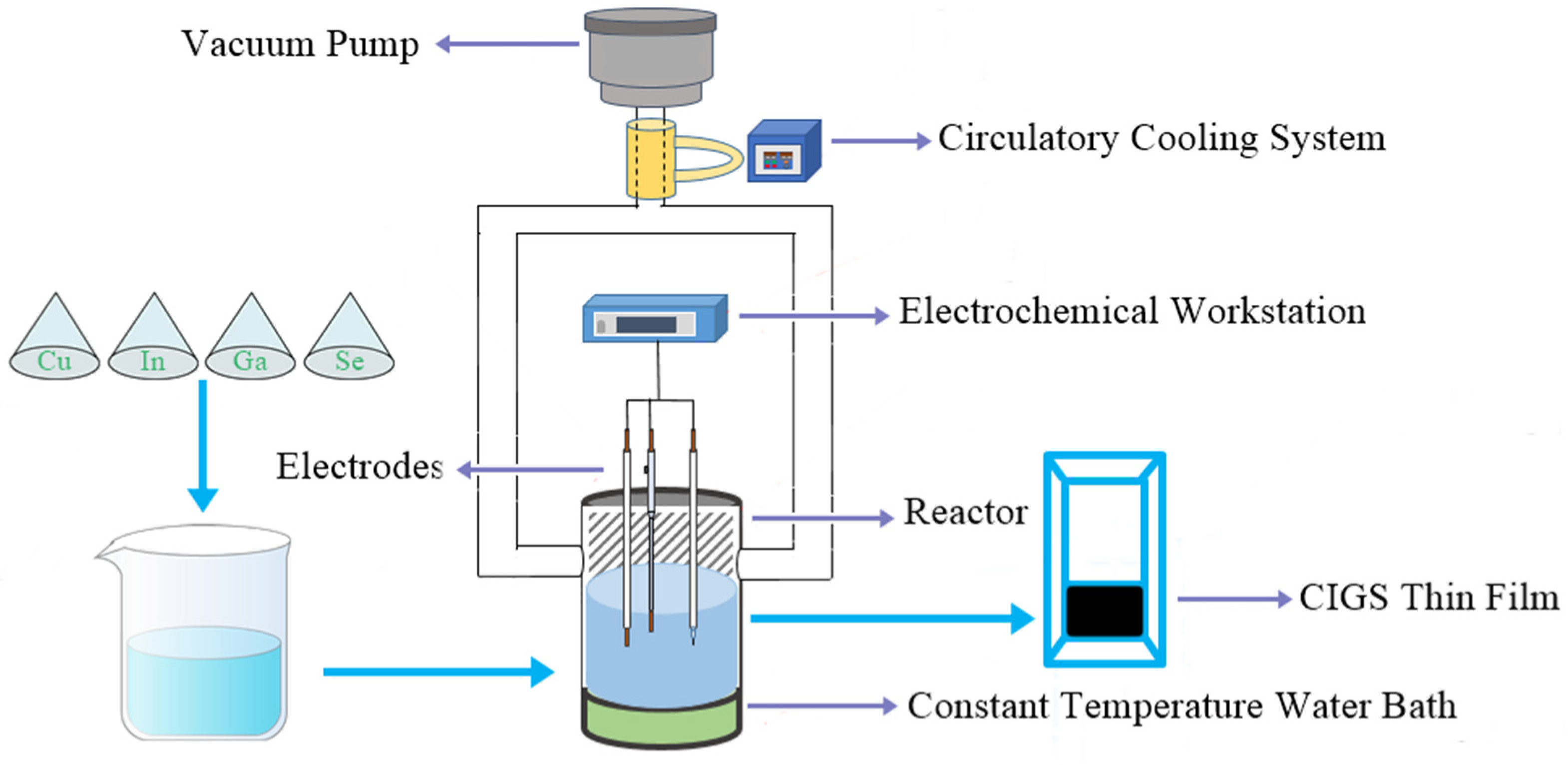
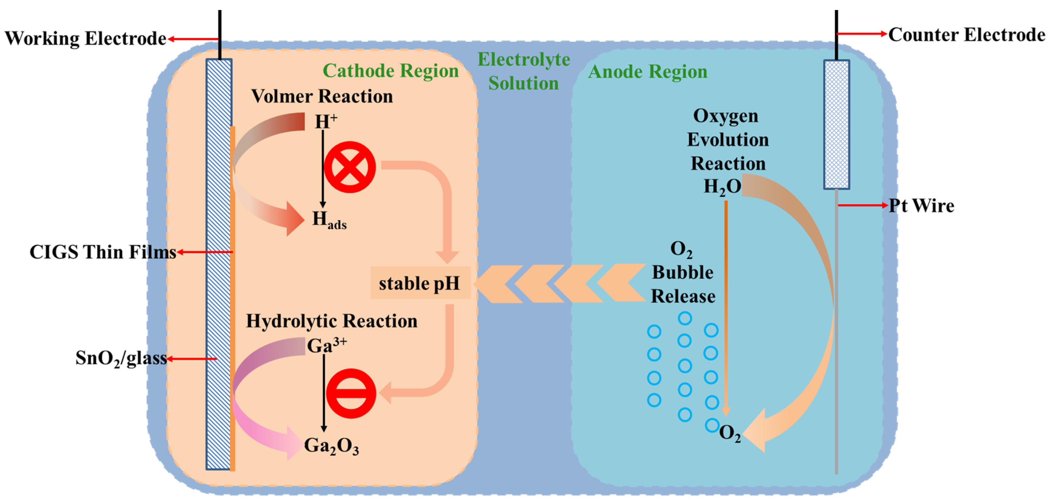
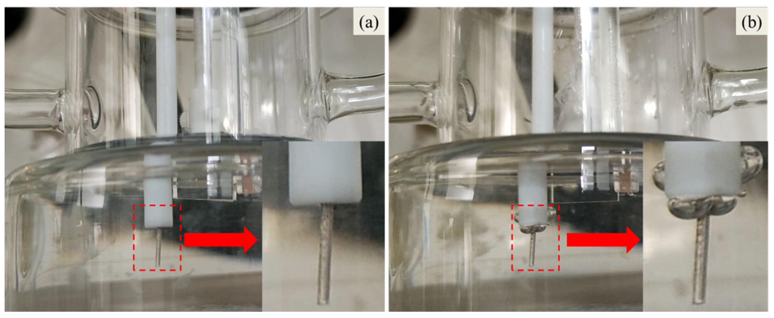
2. Materials and Methods

The electrolyte solution contained 200 mL deionized water with 4 mM CuCl2, 10 mM InCl3, 10 mM GaCl3, 8 mM H2SeO3, and a supporting electrolyte (100 mM LiCl, 100 mM NH4Cl, and 60 mM NH2SO3H). The pH of the solution was adjusted to 1.8 by adding concentrated hydrochloric acid dropwise.
Electrochemical experiments, including linear scanning voltammetry (LSV), potentiostatic polarization, electrochemical impedance spectroscopy (EIS), and electrodeposition were carried out on CIGS thin films in a three-electrode system with a SnO2/glass (1 × 1.5 cm) as the working electrode, a Pt electrode as the counter electrode, and a saturated calomel electrode (SCE) as the reference electrode.
A CorrTest CH310H electrochemical workstation was used for the LSV, potentiostatic polarization, EIS, and electrodeposition CIGS thin film studies. The LSV curves were measured at potentials between 0.1 V to −1.0 V (vs. SCE) with a scanning rate of 10 mV/s. The potentiostatic polarization curves were measured at a potential of −0.60 V (vs. SCE) and a polarization time of 30 min. EIS was performed at a potential of −0.60 V (vs. SCE) with a test frequency range of 0.01 Hz to 100 kHz. On electrodeposited CIGS thin films, the potential range was −0.1 V to −0.9 V (vs. SCE), and the polarization time was 30 min. When the experiment was carried out at 3 kPa, a vacuum pump was used to extract the air from the experimental system for 30 min. Figure 1 illustrates the electrodeposition process of CIGS thin films.
Scanning electron microscopy (SEM, TM3030Plus, Hitachi, Tokyo, Japan) was used to measure the morphology of CIGS thin films, and energy-dispersive spectroscopy (EDS, TM3030Plus, Hitachi, Tokyo, Japan) was utilized to characterize the elemental composition of the CIGS thin films. X-ray diffraction (XRD, Rigaku Ultima IV, Tokyo, Japan), Raman spectroscopy (Raman, DXRxi, Thermo Scientific, MA, USA), and X-ray photoelectron spectroscopy (XPS, Escalab Xi+, Thermo Scientific, MA, USA) were used to characterize the phases in the CIGS thin films.

3. Results and Discussion
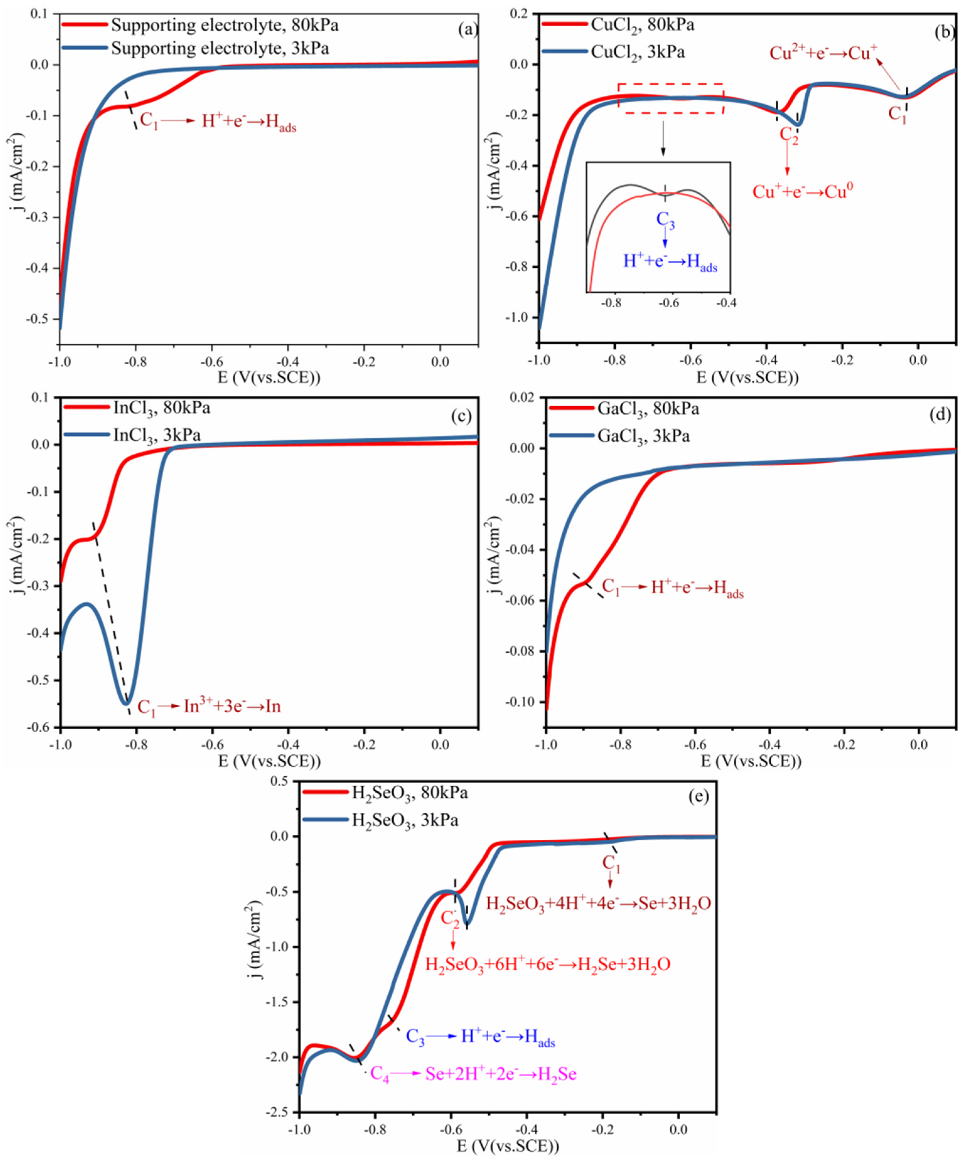
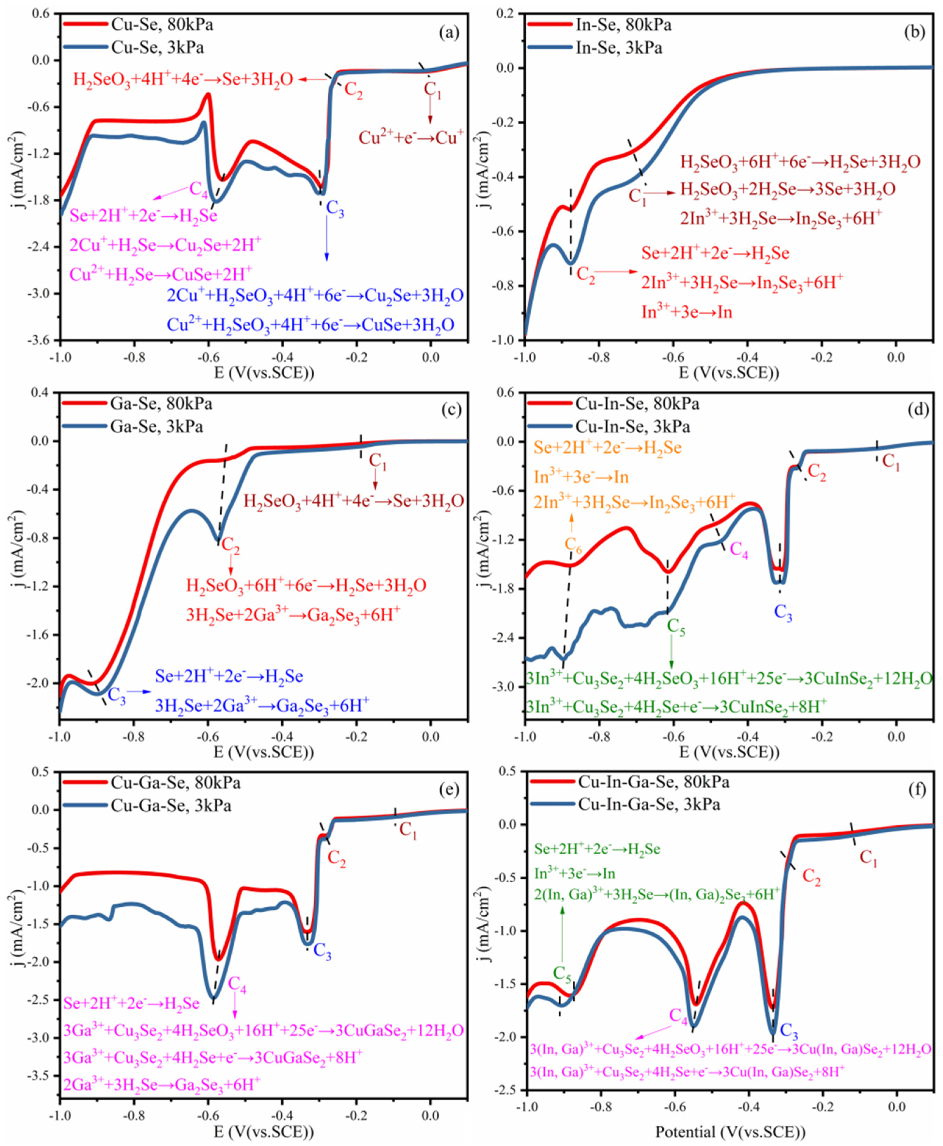
Figure 2 illustrates a schematic of how the vacuum environment affects the electrochemical behavior of Ga3+. In the cathode region, the vacuum environment inhibited the Volmer reaction of H+ to a hydrogen atom (Hads), leading to lower H+ consumption on the cathode surface. In the anode region, the oxygen evolution reaction (OER) of H2O to O2 was promoted, which produced additional O2. At the same time, the rapid release of O2 bubbles agitated the electrolyte solution, which led to a uniform H+ distribution in the electrolyte solution. Thus, the inhibition of the Volmer reaction and the promotion of the OER together stabilized the pH of the cathode region. This finally interrupted the route of Ga3+ entering the films in the form of Ga2O3 by the hydrolytic reaction of Ga3+.

3.1. LSV Analyses

Figure 3a illustrates the effects of the vacuum environment on the hydrogen evolution potentials. Evidence of an inhibited reaction of H+ to Hads was found in a vacuum environment. Peak C1 corresponding to the reaction of H+ to Hads (Equation (1)) did not appear at 3 kPa, possibly due to a decrease in the H2 partial pressure. Because of the reduced partial pressure of H2, the overpotential of H+/Hads on the electrode surface was increased. This phenomenon has also been observed on Au and Pt electrodes [25,26].
H + + e H ads
Figure 3b illustrates the LSV curve of the Cu unary solution at 3 kPa. Peaks C1, C2, and C3 corresponded to the reaction of Cu2+ to Cu+ (Equation (2)), Cu+ to Cu (Equation (3)), and H+ to Hads (Equation (1)), respectively [27]. Peak C1 was indistinguishable at 80 kPa and 3 kPa, indicating that pressure did not affect the reaction of Cu2+ to Cu+. Peak C2 was reduced at 3 kPa, indicating that the formation of Cu was promoted in a low-pressure environment. Peak C3 did not appear at 3 kPa, indicating that the reaction of H+ to Hads was inhibited in a vacuum environment.
Cu 2 + + e Cu +
Cu + + e Cu
Figure 3c illustrates the LSV curve of the In unary solution at 3 kPa. Peak C1 corresponded to the reaction of In3+ to In (Equation (4)) [28]. This peak was reduced at 3 kPa, showing that the formation of In was promoted in a vacuum environment.
I n 3 + + 3 e In
Figure 3d illustrates the LSV curve of the Ga unary solution at 3 kPa. Peak C1 corresponds to the reaction of H+ to Hads [27] (Equation (1)). This peak did not appear at 3 kPa, indicating that the reaction of H+ to Hads was inhibited in a vacuum environment. The reaction of Ga3+ to Ga did not occur within the range of 0.1 V to −1.0 V because the reaction required a higher potential [24].
Figure 3e illustrates the LSV curve of the Se unary solution at 3 kPa. Peaks C1, C2, C3, and C4 corresponded to the reactions of H2SeO3 to Se (Equation (5)), H2SeO3 to H2Se (Equation (6)), H+ to Hads (Equation (1)), and Se to H2Se (Equation (7)), respectively [27]. The current densities of peaks C1, C2, and C4 were greater at 3 kPa, indicating that the formation of H2Se and Se was promoted. Peak C3 did not appear at 3 kPa, indicating that the reaction of H+ to Hads was inhibited in a vacuum environment.
H 2 Se O 3 + 4 H + + 4 e Se + 3 H 2 O
H 2 Se O 3 + 6 H + + 6 e H 2 Se + 3 H 2 O
Se + 2 H + + 2 e H 2 Se
Figure 4a illustrates the LSV curves of Cu-Se binary solutions at 3 kPa. Peaks C1 and C2 corresponded to the formation of Cu+ and Se, respectively (Equations (2) and (5)). Peaks C3 and C4 corresponded to the reaction of H2SeO3 to H2Se and Se to H2Se, respectively (Equations (6) and (7)). Since the solution contained both Cu+ and Cu2+, the two ions were induced by H2SeO3 or H2Se to form Cu2Se or CuSe, respectively [26] (denoted as Cu3Se2 phase) (Equations (8)–(11)). The current densities of peaks C3 and C4 were greater at 3 kPa, indicating that the formation of Cu3Se2 was promoted in a vacuum environment.
2 Cu + + H 2 Se O 3 + 4 H + + 6 e Cu 2 Se + 3 H 2 O
Cu 2 + + H 2 Se O 3 + 4 H + + 6 e Cu Se + 3 H 2 O
2 Cu + + H 2 Se Cu 2 Se + 2 H +
Cu 2 + + H 2 Se Cu Se + 2 H +
Figure 4b illustrates the LSV curves of the In-Se binary solutions at 3 kPa. Peaks C1 and C2 corresponded to the reaction of H2SeO3 to H2Se and Se to H2Se, respectively (Equations (6) and (7)). H2SeO3 reacted with H2Se to form Se (Equation (12)). Because In2Se3 has a high standard Gibbs energy of formation (−386 kJ/mol [29]), H2Se induced In3+ to form In2Se3 [30] (Equation (13)). The current densities of peaks C1 and C2 were greater at 3 kPa, indicating that the formation of H2Se, In2Se3, or In was promoted in a vacuum environment.
2 H 2 Se + H 2 Se O 3 3 Se + 3 H 2 O
3 H 2 Se + 2 In 3 + + 6 e In 2 Se 3
Figure 4c illustrates the LSV curves of Ga-Se binary solutions at 3 kPa. The peaks C1, C2, and C3 correspond to the reaction of H2SeO3 to Se, H2SeO3 to H2Se, and Se to H2Se, respectively (Equations (5)–(7)). Because Ga2Se3 has a high standard Gibbs energy of formation (−418 kJ/mol [31]), Ga3+ was induced by H2Se to form Ga2Se3 [32] (Equation (14)). The current densities of the peaks C2 and C3 are greater at 3 kPa, indicating that the formation of H2Se or Ga2Se3 was promoted in a vacuum environment.
3 H 2 Se + 2 Ga 3 + Ga 2 Se 3 + 6 H +
Figure 4d illustrates the LSV curves of Cu-In-Se ternary solutions at 3 kPa. Peaks C1, C2, C3, C4, and C6 correspond to the formation of Cu+, Se, Cu3Se2, H2Se, and In2Se3 or In, respectively (Equations (2), (5), (8)–(11), (6), (13) or (4)). In3+ was induced by Cu3Se2 + H2SeO3 or Cu3Se2 + H2Se to produce more stable CuInSe2 [32] (Equations (15) and (16)) at peak C5. As the polarization potential increased, the current density became greater at 3 kPa, indicating that the formation of CIS was promoted in a vacuum environment.
3 In 3 + + Cu 3 Se 2 + 4 H 2 Se O 3 + 16 H + + 25 e 3 CuIn Se 2 + 12 H 2 O
3 In 3 + + Cu 3 Se 2 + 4 H 2 Se + e 3 CuIn Se 2 + 8 H +
Figure 4e illustrates the LSV curves of Cu-Ga-Se ternary solutions at 3 kPa. Peaks C1, C2, C3, and C4 corresponded to the formation of Cu+, Se, Cu3Se2, and Ga2Se3, respectively (Equations (2), (5), (8)–(11) and (14)). Ga3+ was induced by Cu3Se2 + H2SeO3 or Cu3Se2 + H2Se to produce CuGaSe2 [31] (Equations (17) and (18)) at peak C4. As the polarization potential increased, the current density became greater at 3 kPa, indicating that the formation of CGS was promoted in a vacuum environment.
3 Ga 3 + + Cu 3 Se 2 + 4 H 2 Se O 3 + 16 H + + 25 e 3 Cu Ga Se 2 + 12 H 2 O
3 Ga 3 + + Cu 3 Se 2 + 4 H 2 Se + e 3 Cu Ga Se 2 + 8 H +
Figure 4f illustrates the LSV curves of Cu-In-Ga-Se ternary solutions at 3 kPa. Peaks C1, C2, and C3 corresponded to the formation of Cu+, Se, and Cu3Se2, respectively (Equations (2), (5), (8)–(11)). Ga and In are homotopic elements, and their reduction processes at the cathode are similar (noted as (In, Ga)3+ phase). Meanwhile, both In3+ and Ga3+ were induced by Cu3Se2 + H2SeO3 or Cu3Se2 + H2Se into the films (Equations (15)–(18)). Therefore, In3+ and Ga3+ competed for reduction at the cathode. According to previous conclusions, the reduction potential of In and Ga in the CIGS thin films was −0.6 V. Therefore, peak C4 corresponded to the formation of CuInSe2, CuGaSe2, or Cu(In, Ga)Se2 (Equations (19) and (20)). Peak C5 corresponded to the formation of In2Se3, Ga2Se3, or In (Equations (13), (14), or (4)). The current density of peak C4 was greater at 3 kPa, indicating that the formation of CIGS was promoted in a vacuum environment.
3 ( In ,   Ga ) 3 + + Cu 3 Se 2 + 4 H 2 Se O 3 + 16 H + + 25 e 3 Cu ( In ,   Ga ) Se 2 + 12 H 2 O
3 ( In ,   Ga ) 3 + + Cu 3 Se 2 + 4 H 2 Se + e 3 Cu ( In ,   Ga ) Se 2 + 8 H +

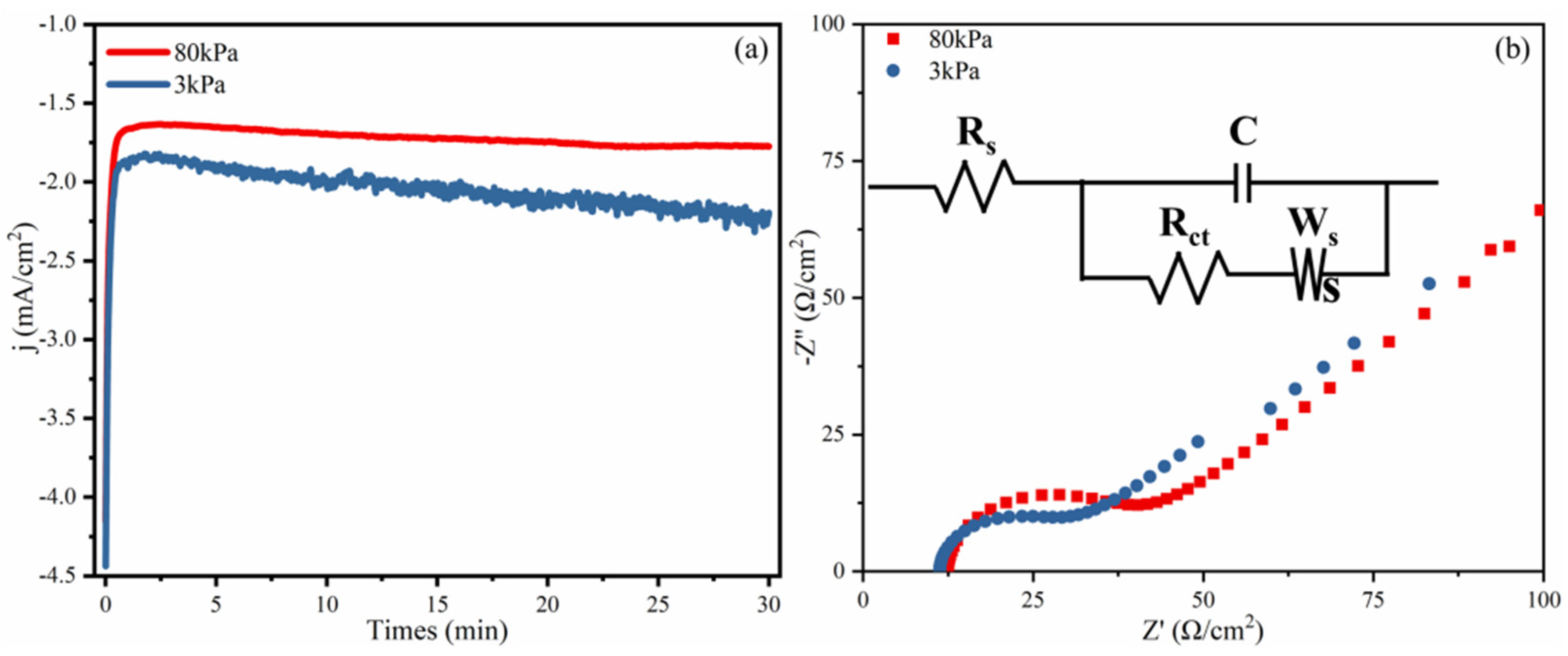
3.2. Potentiostatic Polarization and EIS Analyses
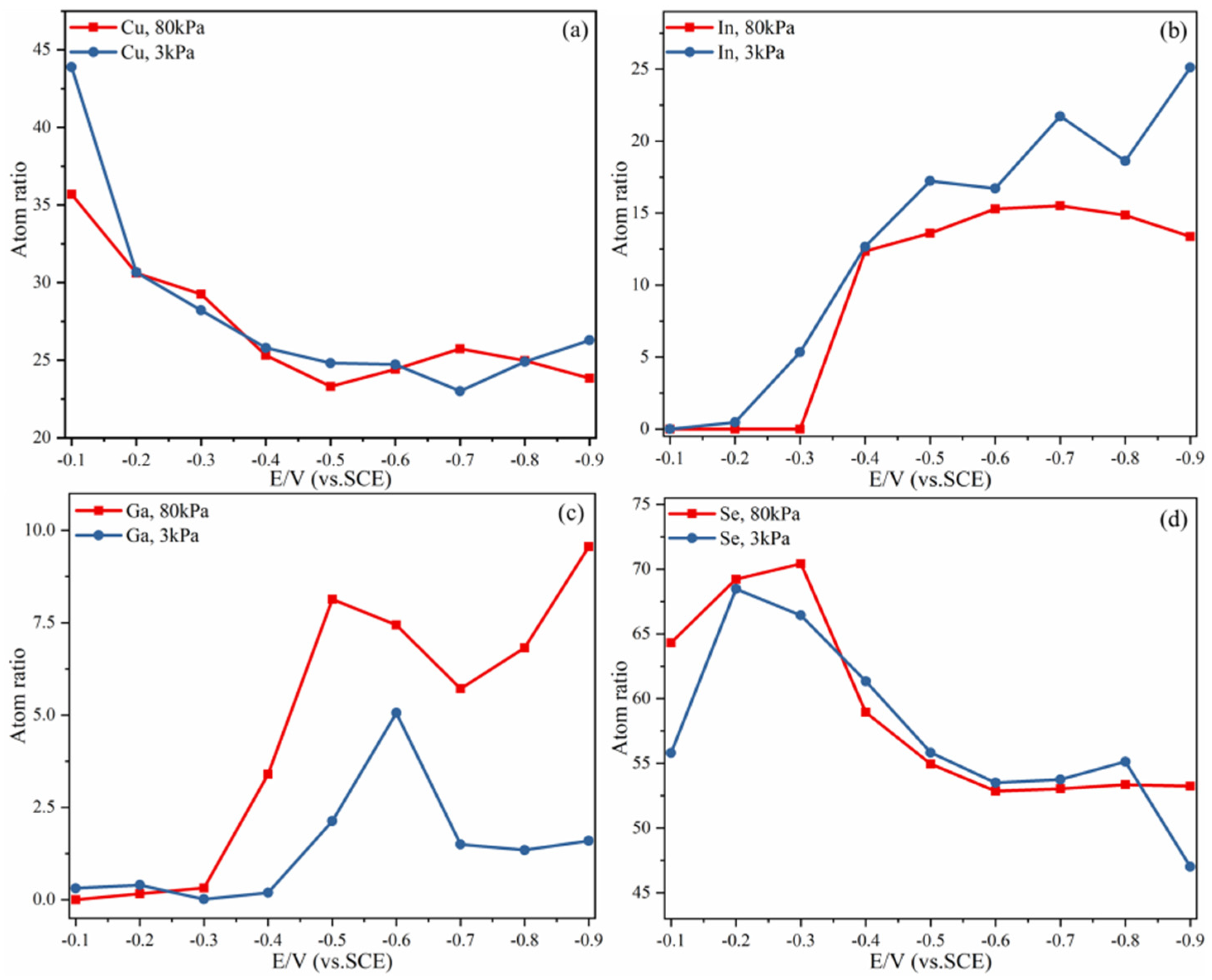
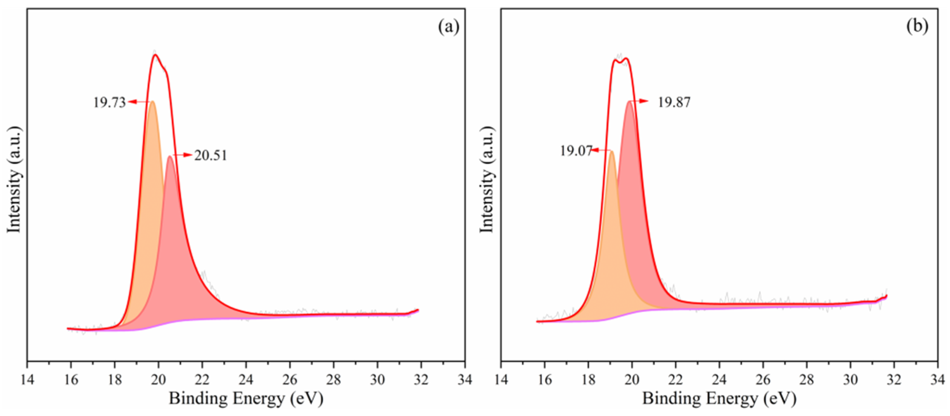
According to the previous conclusion, the main reduction potential of In3+ and Ga3+ in the CIGS thin films was −0.6 V. Therefore, the potentiostatic polarization potential was set to −0.6 V. Figure 5a illustrates the potentiostatic polarization curve of the CIGS thin films at 3 kPa. The current density was always greater at 3 kPa, indicating that the resistance during the preparation of CIGS thin films was lower in a vacuum environment.
Changes in the diffusion impedance and charge-transfer impedance during the preparation of CIGS thin films were investigated by EIS at a low pressure. Figure 5b illustrates the impedance Nyquist plot of the CIGS thin films deposition process at 3 kPa. The semicircle diameter of the curve was smaller, and the slope of the straight line was larger at 3 kPa, indicating that the electroreduction and diffusion impedances were lower, respectively. In addition, the ohmic impedance was smaller. Thus, the resistance was lower when applying vacuum electrodeposition. This corresponds to the conclusion of the current density-time curves. Both curves in Figure 5b were semicircular with straight lines, indicating that electroreduction and diffusion controlled the CIGS thin films deposition [33].
In this study, the impedance test data were combined in order to fit the equivalent circuit of the CIGS thin films deposition process. The fitted EIS data of the CIGS thin films deposition process at different pressures are shown in Table 1. Ws is the Warburg diffusion impedance, Rct is the charge-transfer impedance between the interface of cathode and electrolyte solutions, C is the electrical double-layer capacitance on the electrode surface, and Rs is the electrolyte solution impedance.
When the system pressure was reduced from 80 kPa to 3 kPa, Ws fell by 69.1%, Rct fell by 29.6%, C rose by 35.4%, and Rs remained constant. Figure 6 illustrates the OER on the anode surface during the preparation of the CIGS thin films. At 3 kPa, the number of bubbles at the Pt electrode was higher, and the volume was larger. Therefore, the formation of O2 was promoted under a vacuum. The promoted formation of O2 indicates that the electrode reaction proceeded more smoothly. The smooth occurrence of the electrode reaction was also one of the reasons for the higher current density at 3 kPa. In addition, according to Boyle’s law, the bubble volume should be larger in a vacuum environment. This is consistent with the phenomenon in Figure 6. The rapid release of O2 bubbles enhanced the diffusion of the electrolyte solution. Therefore, the Ws value fell. Since the reaction of H+ to Hads was inhibited, and the rapid dehydrogenation occurred in the electrolyte at 3 kPa, the contact area increased between the interface of the cathode and electrolyte solution, which decreased the Rct value. Because the reaction of H+ to Hads was inhibited, the deposition of major elements increased. Thus, the thickness of the CIGS thin films increased, which increased the C value at 3 kPa. Because it was determined by the electrolyte solution, the Rs value remained constant.

3.3. EDS Analysis

Figure 7 illustrates the EDS composition curves of Cu, In, Ga, and Se in CIGS thin films at polarization potentials from −0.1 V to −0.9 V. Overall, changing the pressure had little effect on the element deposition pattern but had a significant impact on the elemental content. Combined with Figure 3, the first reduction potentials of Cu and Se were 0 V and −0.2 V, respectively. Therefore, Cu ions were more easily reduced when the reduction potential was −0.1 V. As shown in Figure 7a, the content of Cu in the films was highest at this time. The formation of Cu and Cu3Se2 was promoted in a vacuum environment, which in turn led to a high content of Cu in the films at 3 kPa. When the reduction potential was −0.2 V, the reduction of Se became easier. As shown in Figure 7d, the content of Se in the films increased. As the potential increases, the Cu and Se content tended to be relatively stable. As a whole, the content of Cu and Se in the CIGS thin films was slightly higher at 3 kPa, indicating that the vacuum environment was beneficial for the formation of Cu and Se.
As shown in Figure 7b, the potential of In in the CIGS thin films was −0.2 V at 3 kPa. However, this potential was −0.4 V at 80 kPa. The reason may be that the formation of Cu3Se2 was promoted in a vacuum environment and In was induced by the excess Cu3Se2 to produce a more stable CuInSe2 phase, which in turn could enter the films at a lower potential. Meanwhile, the content of In in the films was higher at 3 kPa. As a result, the formation of In was promoted in a vacuum environment.
As shown in Figure 7c, when the potential was lower, the formation of Ga was largely unaffected due to the lower In content in the films. Because the In content in the films increased as the potential increased, and the formation of In and Ga had a competitive relationship, the formation of Ga was inhibited. This was the first reason for the low concentration of Ga in the CIGS thin films at 3 kPa. Upon increasing the potential, the production of H2 at the cathode surface increased at 80 kPa. In turn, the consumption of H+ in the cathode region increased. Along with the consumption of H+, the pH at the cathode region increased, which led to the hydrolysis of Ga3+ to Ga2O3 [24]. Ga3+ entered the films in the form of Ga2O3 [23]. Because the reaction of H+ to Hads was inhibited and the OER was promoted at 3 kPa, the pH remained relatively stable at the cathode region, which prevented Ga3+ from entering the films in the form of Ga2O3. This was the second reason for the low Ga concentration in the CIGS thin films at 3 kPa. In summary, the formation of Ga was inhibited in a vacuum environment.

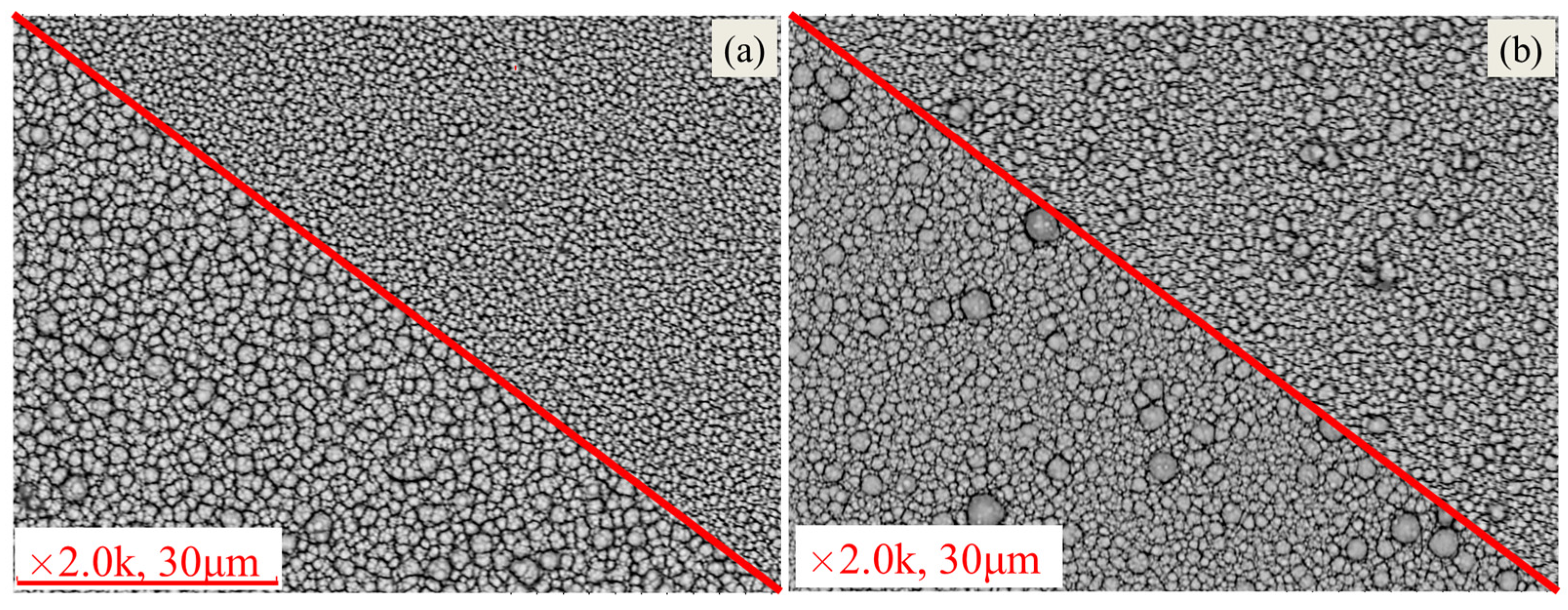
3.4. Morphologic Analyses
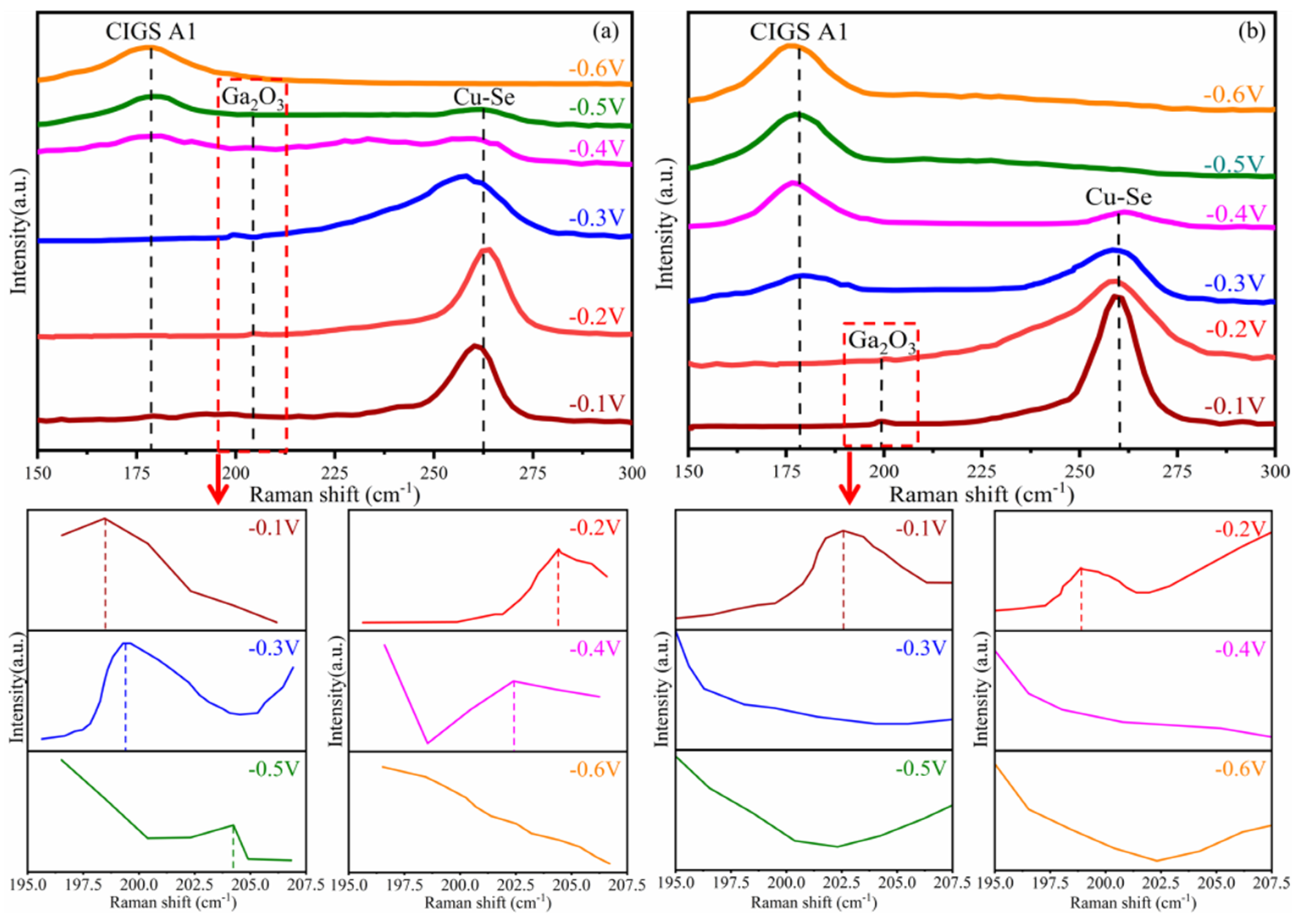
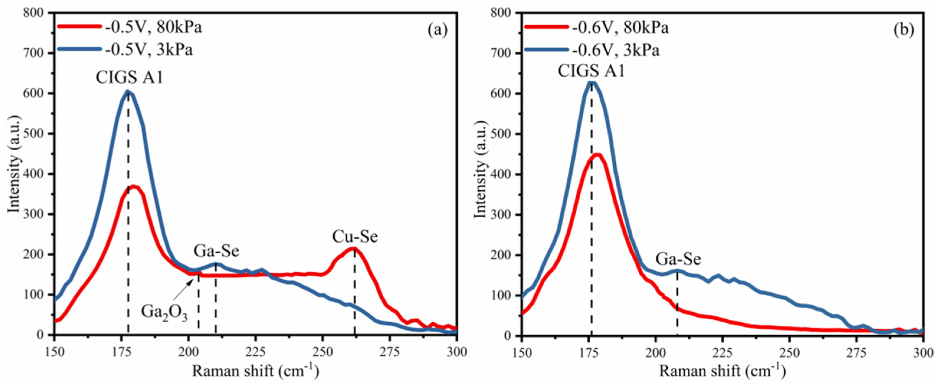
SEM images showing the morphologies of the CIGS thin films prepared at various deposition potentials and pressures are displayed in Figure 8. Overall, the particles [29] in the films were larger at 3 kPa. The first reason is that the reaction of H+ to Hads was inhibited, which in turn inhibited H2 production. Another reason is that the vacuum environment quickly removed H2 from the surface of the CIGS thin films. The amount of H2 adsorbed on the cathode surface decreased, and the space available for the deposition of major elements increased.

3.5. Phase Analyses

As shown in Figure 9, in the CIGS thin films, there are three main diffraction peaks due to (101), (112), and (220) planes corresponding to CuIn0.7Ga0.3Se2. The positions of these diffraction peaks are quite similar. In addition, the difference in pressure changes the preferred crystallographic orientation. When the pressure is 80 kPa, the CuIn0.7Ga0.3Se2 phase possesses a (101) preferred crystallographic orientation at approximately 17.27°. However, under 3 kPa, the preferred crystallographic orientation is a (112) plane located at approximately 26.90°. For the CuIn0.7Ga0.3Se2 phase, a preference for the (112) plane is more favorable. Therefore, the main CuIn0.7Ga0.3Se2 phase can be electrochemically deposited at the pressure of 80 kPa and even at 3 kPa, although with different preferred crystallographic orientations.
The surface phases were characterized by Raman spectroscopy, as shown in Figure 10 and Figure 11. According to Figure 10a, the vibrational peaks of the Ga2O3 phase (200 cm−1 [34]) appeared in the potential range from −0.1 V to −0.2 V at both 80 kPa and 3 kPa. This was because the reaction of H2SeO3 to Se consumed H+ in the cathode region, which in turn hydrolyzed Ga to Ga2O3 in the films [35]. Meanwhile, little O2 formed on the anode surface due to the low potential and could not increase the mass transfer rate of the solution at 3 kPa. This was why the Ga2O3 phase appeared at a low potential at 3 kPa.
When the potential was −0.3 V, the main phase of the films changed from the Cu-Se phase (260 cm−1 [36]) to the CIGS A1 phase (175 cm−1 [37]) at 3 kPa. The formation of the CIGS A1 phase led to a decrease in the consumption of H+. Increasing the potential led to a gradual increase in the O2 production, which in turn led to a gradual increase in the mass transfer rate, resulting in a stable pH in the cathode region. Ga3+ hydrolysis was inhibited, and the Ga2O3 phase disappeared. However, at 80 kPa, when the potential was −0.4 V, only the main phase of the films began to transform. In correspondence with the higher potential, the hydrogen evolution reaction began to occur. Therefore, the vibrational peak of the Ga2O3 phase was always present when the potential was in the range of −0.3 V to −0.5 V.
As shown in Figure 11, Ga entered the films as Ga-Se phase (214 cm−1 [38]) at 3 kPa. Combined with the above conclusions, the formation of Ga2O3 was inhibited at 3 kPa.
Since poorly-crystallized Ga2O3 did not produce a Raman response, this article determined the phase of Ga from the Ga 3d binding energy. The XPS spectra of the CIGS thin films are presented in Figure 12. According to Figure 11, at 80 kPa, the binding energy of 19.73 eV and 20.51 eV are related to Ga of CIGS thin films, and at 3 kPa, 19.07 eV and 19.87 eV are related to Ga of CIGS thin films. According to the literature, 19.07 eV corresponds to GaSe (19.00 eV, Ga 3d) [39], and 19.73 eV and 19.87 eV correspond to Ga2Se3 (19.70 eV or 19.90 eV, Ga 3d5/2) [40]. In addition, 20.51 eV is close to Ga2O3 (20.50 eV, Ga 3d5/2) [41]. In summary, the phases of the films were Ga2Se3 and Ga2O3 at 80 kPa, while GaSe and Ga2Se3 were the phases at 3 kPa. That is to say, the formation of Ga2O3 must be inhibited in a vacuum environment.

4. Conclusions

In this article, CIGS films without a low-conductivity Ga2O3 phase were prepared using vacuum electrodeposition, as supported by the conclusions of Raman and XPS. There were two main reasons for the inhibited Ga2O3 formation. The first reason is the inhibition of the H+ to Hads reaction, which decreased the consumption of H+ on the cathode surface, as confirmed by the disappearance of the Hads generation peak in the LSV curve. The second reason is that the OER reaction was promoted by a smoother electrode reaction and a decrease in the electrochemical impedance during deposition. The larger current density in the current density-time curves and the smaller semicircle diameter in the impedance Nyquist plots confirmed this. The inhibition of the H+ to Hads reaction and the promotion of the OER together stabilized the pH in the cathode region, which in turn inhibited Ga3+ hydrolysis. The path of Ga3+ into the films in the form of Ga2O3 was blocked.
In a vacuum environment, the content of Cu, In, and Se in the films increased, the current density of the preparation process increased, and the resistance decreased. The increase in the deposition space of the main elements produced larger particles in the films.

Author Contributions

In this joint work, each author was in charge of their expertise and capability: Conceptualization, G.L.; methodology, K.H.; validation, J.Z.; formal analysis, K.H.; investigation, K.H.; resources, L.X.; data curation, W.W.; writing—original draft preparation, G.L.; writing—review and editing, J.Y.; supervision, B.Y.; project administration, B.X.; funding acquisition, J.Y. All authors have read and agreed to the published version of the manuscript.

Funding

This research was funded by the National Natural Science Foundation of China grant number 52104350 and 52264038, the Natural Science Foundation of Yunnan Province grant number 202001AT070045, National Key Research and Development Program of China grant number 2022YFC2904204.

Data Availability Statement

The data presented in this study are available on request from the corresponding author. The data are not publicly available due to unfinished related ongoing further studies.

Conflicts of Interest

The authors declare no conflict of interest. The funders had no role in the design of the study, in the collection, analyses, or interpretation of data, in the writing of the manuscript, or in the decision to publish the results.

References

  1. Kang, C.; Lee, G.; Lee, W.; Cho, D.H.; Maeng, I.; Chung, Y.D.; Kee, C.S. Terahertz Emission and Ultrafast Carrier Dynamics of Ar-Ion Implanted Cu(In, Ga)Se2 Thin Films. Crystals 2021, 11, 411. [Google Scholar] [CrossRef]
  2. Jiang, J.; Giridharagopal, R.; Jedlicka, E.; Sun, K.; Yu, S.; Wu, S.; Gong, Y.; Yan, W.; Ginger, D.S.; Green, M.A.; et al. Highly efficient copper-rich chalcopyrite solar cells from DMF molecular solution. Nano Energy 2020, 69, 104438. [Google Scholar] [CrossRef]
  3. Hedayati, M.; Olyaee, S. High-Efficiency p-n Homojunction Perovskite and CIGS Tandem Solar Cell. Crystals 2022, 12, 703. [Google Scholar] [CrossRef]
  4. Huang, C.H.; Chuang, W.J.; Lin, C.P.; Jan, Y.L.; Shih, Y.C. Deposition Technologies of High-Efficiency CIGS Solar Cells: Development of Two-Step and Co-Evaporation Processes. Crystals 2018, 8, 296. [Google Scholar] [CrossRef] [Green Version]
  5. Ma, Q.; Zhang, W.; Jiang, Z.; Ma, D.; Zhang, Y.; Lu, C.; Fan, Z. The Formation Mechanism of Cu(In0.7 Ga0.3)Se2 Nanoparticles and the Densification Trajectory of the Se-Rich Quaternary Target by Hot Pressing. Crystals 2018, 8, 135. [Google Scholar] [CrossRef] [Green Version]
  6. Altaf, C.T.; Sahsuvar, N.S.; Abdullayeva, N.; Coskun, O.; Kumtepe, A.; Karagoz, E.; Sankir, M.; Sankir, N.D. Inverted Configuration of Cu(In, Ga)S2/In2S3 on 3D-ZnO/ZnSnO3 Bilayer System for Highly Efficient Photoelectrochemical Water Splitting. ACS. Sustain. Chem. Eng. 2020, 8, 15209–15222. [Google Scholar] [CrossRef]
  7. Matur, U.C.; Baydogan, N. Changes in gamma attenuation behaviour of sol-gel derived CIGS thin film irradiated using Co-60 radioisotope. J. Alloys Compd. 2017, 695, 1405–1413. [Google Scholar] [CrossRef]
  8. Ao, J.; Fu, R.; Jeng, M.J.; Bi, J.; Yao, L.; Gao, S.; Sun, G.; He, Q.; Zhou, Z.; Sun, Y.; et al. Formation of Cl-Doped ZnO Thin Films by a Cathodic Electrodeposition for Use as a Window Layer in CIGS Solar Cells. Materials 2018, 11, 953. [Google Scholar] [CrossRef] [Green Version]
  9. Oliveri, R.L.; Patella, B.; Pisa, F.D.; Mangione, A.; Aiello, G.; Inguanta, R. Fabrication of CZTSe/CIGS Nanowire Arrays by One-Step Electrodeposition for Solar-Cell Application. Materials 2021, 14, 2778. [Google Scholar] [CrossRef]
  10. Péter, L.; Fekete, É.; Kapoor, G.; Gubicza, J. Influence of the preparation conditions on the microstructure of electrodeposited nanocrystalline Ni–Mo alloys. Electrochim. Acta 2021, 382, 138352. [Google Scholar] [CrossRef]
  11. Beltowska-Lehman, E.; Bigos, A.; Indyka, P.; Kot, M. Electrodeposition and characterisation of nanocrystalline Ni–Mo coatings. Surf. Coat. Technol. 2012, 211, 67–71. [Google Scholar] [CrossRef]
  12. Ren, Y.; Ma, W.; Wei, K.; Yu, W.; Dai, Y.; Morita, K. Degassing of aluminum alloys via the electromagnetic directional solidification. Vacuum 2014, 109, 82–85. [Google Scholar] [CrossRef]
  13. Fromm, E. Maximum rate of sorption and degassing processes in vacuum metallurgical treatments. Vacuum 1971, 21, 585–586. [Google Scholar] [CrossRef]
  14. Pessel, L. Apparatus for electroplating metal. U.S. Patent 2465747, 30 April 1945. [Google Scholar]
  15. Muttilainen, E.; Tunturi, P.J. Hard chromium plating under reduced pressure improves corrosion resistance. Anti-Corros. Method. M. 1984, 31, 13–15. [Google Scholar] [CrossRef]
  16. Nam, S.E.; Lee, S.H.; Lee, K.H. Preparation of a palladium alloy composite membrane supported in a porous stainless steel by vacuum electrodeposition. J. Membrane. Sci. 1999, 153, 163–173. [Google Scholar] [CrossRef]
  17. Nam, S.E.; Seong, Y.K.; Lee, J.W.; Lee, K.H. Preparation of highly stable palladium alloy composite membranes for hydrogen separation. Desalination 2007, 236, 51–55. [Google Scholar] [CrossRef]
  18. Su, R.; Lü, Z.; Chen, K.; Ai, N.; Li, S.; Wei, B.; Su, W. Novel in situ method (vacuum assisted electroless plating) modified porous cathode for solid oxide fuel cells. Electrochem. Commun. 2008, 10, 844–847. [Google Scholar] [CrossRef]
  19. Ming, P.; Zhu, D.; Hu, Y.; Zeng, Y. Micro-electroforming under periodic vacuum-degassing and temperature-gradient conditions. Vacuum 2009, 83, 1191–1199. [Google Scholar] [CrossRef]
  20. Ming, P.; Li, Y.; Wang, S.; Li, S.; Li, X. Microstructure and properties of nickel prepared by electrolyte vacuum boiling electrodeposition. Surf. Coat. Technol. 2012, 213, 299–306. [Google Scholar] [CrossRef]
  21. Hibberd, C.J.; Chassaing, E.; Liu, W.; Mitzi, D.B.; Lincot, D.; Tiwari, A.N. Non-vacuum methods for formation of Cu(In, Ga)(Se, S)2 thin film photovoltaic absorbers. Prog. Photovoltaics. 2010, 18, 434–452. [Google Scholar] [CrossRef]
  22. Estela Calixto, M.; Dobson, K.D.; McCandless, B.E.; Birkmire, R.W. Controlling Growth Chemistry and Morphology of Single-Bath Electrodeposited Cu(In, Ga)Se2 Thin Films for Photovoltaic Application. J. Electrochem. Soc. 2006, 153, G521–G528. [Google Scholar] [CrossRef]
  23. Yang, J.; Huang, C.; Jiang, L.; Liu, F.; Lai, Y.; Li, J.; Liu, Y. Effects of hydrogen peroxide on electrodeposition of Cu(In, Ga)Se2 Thin films and band gap controlling. Electrochim. Acta 2014, 142, 208–214. [Google Scholar] [CrossRef]
  24. Flamini, D.O.; Saidman, S.B.; Bessone, J.B. Electrodeposition of gallium onto vitreous carbon. J. Appl. Electrochem. 2007, 37, 467–471. [Google Scholar] [CrossRef]
  25. Murray, R.; Sigmund, S. The H+/H2 equilibrium potential dependence on H2 partial pressure on gold electrodes. Electrochim. Acta 1973, 18, 687–690. [Google Scholar]
  26. Warner, T.B.; Schuldiner, S. Potential of a Platinum Electrode at Low Partial Pressures of Hydrogen or Oxygen. J. Electrochem. Soc. 1965, 112, 853–856. [Google Scholar] [CrossRef]
  27. Liu, J.; Liu, F.; Lai, Y.; Zhang, Z.; Li, J.; Liu, Y. Effects of sodium sulfamate on electrodeposition of Cu(In, Ga)Se2 thin film. Electroanal. Chem. 2011, 651, 191–196. [Google Scholar] [CrossRef]
  28. Lai, Y.; Liu, F.; Zhang, Z.; Liu, J.; Li, Y.; Kuang, S.; Li, J.; Liu, Y. Cyclic voltammetry study of electrodeposition of Cu(In, Ga)Se2 thin films. Electrochim. Acta. 2008, 54, 3004–3010. [Google Scholar] [CrossRef]
  29. Lincot, D.; Guillemoles, J.F.; Taunier, S.; Guimard, D.; Sicx-Kurdi, J.; Chaumont, A.; Roussel, O.; Ramdani, O.; Hubert, C.; Fauvarque, J.P.; et al. Chalcopyrite thin film solar cells by electrodeposition. Sol. Energy. 2004, 77, 725–737. [Google Scholar] [CrossRef]
  30. Lai, Y.; Liu, J.; Yang, J.; Wang, B.; Liu, F.; Zhang, Z.; Li, J.; Liu, Y. Incorporation Mechanism of Indium and Gallium during Electrodeposition of Cu(In, Ga)Se2 Thin Film. J. Electrochem. Soc. 2011, 158, D704–D709. [Google Scholar] [CrossRef]
  31. Lai, Y.; Liu, F.; Li, J.; Zhang, Z.; Liu, Y. Nucleation and growth of selenium electrodeposition onto tin oxide electrode. Electroanal. Chem. 2010, 639, 187–192. [Google Scholar] [CrossRef]
  32. Kemell, M.; Ritala, M.; Saloniemi, H.; Leskelä, M.; Sajavaara, T.; Rauhala, E. One-Step Electrodeposition of Cu2-xSe and CuInSe2 Thin Films by the Induced Co-deposition Mechanism. J. Electrochem. Soc. 2000, 147, 1080–1087. [Google Scholar] [CrossRef]
  33. You, R.; Lew, K.K.; Fu, Y.P. Effect of indium concentration on electrochemical properties of electrode-electrolyte interface of CuIn1−xGaxSe2 prepared by electrodeposition. Mater. Res. Bull. 2017, 96, 183–187. [Google Scholar] [CrossRef]
  34. Gonzalo, A.; Nogales, E.; Lorenz, K.; Víllora, E.G.; Shimamura, K.; Piqueras, J.; Méndez, B. Raman and cathodoluminescence analysis of transition metal ion implanted Ga2O3 nanowires. J. Lumin. 2017, 191, 56–60. [Google Scholar] [CrossRef]
  35. Liu, F.; Yang, J.; Zhou, J.; Lai, Y.; Jia, M.; Li, J.; Liu, Y. One-step electrodeposition of CuGaSe2 thin films. Thin Solid Films 2012, 520, 2781–2784. [Google Scholar] [CrossRef]
  36. Ren, T.; Yu, R.; Zhong, M.; Shi, J.; Li, C. Microstructure evolution of CuInSe2 thin films prepared by single-bath electrodeposition. Sol. Energ. Mat. Sol. C 2010, 95, 510–520. [Google Scholar] [CrossRef]
  37. Insignares-Cuello, C.; Izquierdo-Roca, V.; López-García, J.; Calvo-Barrio, L.; Saucedo, E.; Kretzschmar, S.; Unold, T.; Broussillou, C.; Goislard de Monsabert, T.; Bermudez, V.; et al. Combined Raman scattering/photoluminescence analysis of Cu(In, Ga)Se2 electrodeposited layers. Solar Energy 2014, 103, 89–95. [Google Scholar] [CrossRef]
  38. Bergeron, A.; Ibrahim, J.; Leonelli, R.; Francoeur, S. Oxidation dynamics of ultrathin GaSe probed through Raman spectroscopy. Appl. Phys. Lett. 2017, 110, 241901. [Google Scholar] [CrossRef] [Green Version]
  39. Lang, O.; Tomm, Y.; Schlaf, R.; Pettenkofer, C.; Jaegermann, W. Single crystalline GaSe/WSe2 heterointerfaces grown by van der Waals epitaxy. II. Junction characterization. J. Appl. Phys. 1994, 75, 7814–7820. [Google Scholar] [CrossRef]
  40. Iwakuro, H.; Tatsuyama, C.; Ichimura, S. XPS and AES Studies on the Oxidation of Layered Semiconductor GaSe. Jpn. J. Appl. Phys. 1982, 21, 94–99. [Google Scholar] [CrossRef]
  41. Carli, R.; Bianchi, C.L. XPS analysis of gallium oxides. Appl. Surf. Sci. 1994, 74, 99–102. [Google Scholar] [CrossRef]
Figure 1. A schematic of the electrodeposition CIGS thin films system.
Crystals 13 00319 g001
Figure 2. Schematic illustration for the inhibition of Ga3+ hydrolysis in 3 kPa.
Crystals 13 00319 g002
Figure 3. The LSV curves in the (a) supporting electrolyte, (b) 4 mM CuCl2, (c) 10 mM InCl3, (d) 10 mM GaCl3, and (e) 8 mM H2SeO3 unary solutions at 3 kPa.
Crystals 13 00319 g003
Figure 4. The LSV curves in the (a) Cu−Se, (b) In−Se (c) Ga−Se binary, (d) Cu−In−Se, (e) Cu−Ga−Se ternary, and (f) Cu−In−Ga−Se quaternary solutions at 3 kPa.
Crystals 13 00319 g004
Figure 5. The (a) current density−time curve and (b) impedance Nyquist plot of electrodeposition CIGS thin films at 3 kPa.
Crystals 13 00319 g005
Figure 6. The picture of the OER on the anode surface at pressures of (a) 80 kPa and (b) 3 kPa.
Crystals 13 00319 g006
Figure 7. EDS composition curves of (a) Cu, (b) In, (c) Ga, and (d) Se in CIGS thin films.
Crystals 13 00319 g007
Figure 8. SEM images of the morphology of CIGS thin films prepared at the pressures of 80 kPa (above the red diagonal line) and 3 kPa (below the red diagonal line) and at the potentials of (a) −0.5 V and (b) −0.6 V.
Crystals 13 00319 g008
Figure 9. XRD spectra of CIGS thin film prepared at the potential of −0.6 V and pressures of: (a) 80 kPa and (b) 3 kPa.
Crystals 13 00319 g009
Figure 10. Raman spectra of CIGS thin film prepared at potentials of −0.1 V to −0.6 V and pressures of: (a) 80 kPa and (b) 3 kPa.
Crystals 13 00319 g010
Figure 11. Raman spectra of CIGS thin films prepared at pressures of 80 kPa and 3 kPa and at potentials of (a) −0.5 V and (b) −0.6 V.
Crystals 13 00319 g011
Figure 12. Binding energy of Ga 3d in CIGS thin films prepared at the potential of −0.6 V and pressures of (a) 80 kPa and (b) 3 kPa.
Crystals 13 00319 g012
Table 1. Fitting data of CIGS thin films deposition impedance at 3 kPa (Ω).
PressureWsRctCRs
80 kPa417.642.392.292 × 10−418.77
3 kPa129.129.833.546 × 10−419.23
Disclaimer/Publisher’s Note: The statements, opinions and data contained in all publications are solely those of the individual author(s) and contributor(s) and not of MDPI and/or the editor(s). MDPI and/or the editor(s) disclaim responsibility for any injury to people or property resulting from any ideas, methods, instructions or products referred to in the content.

