1. Introduction
Fused silica is an important component of large high-power laser devices and electro-optic information systems [
1,
2]. Surface damage frequently occurs in the process of high-throughput operation. The damage point will expand dramatically if it is not repaired in time, which will degrade the property of the fused silica and even damage other components [
3,
4]. The optical element can be repaired by removing the damaged point and the surrounding material. This will ensure the economical and stable operation of the device. Traditional damage repair methods mainly include CO
2 laser ablation and femtosecond excision. The material around the damage point is vaporized using the focal point of the CO
2 laser [
5,
6,
7,
8] or femtosecond laser [
9,
10]. The scanning track of the focus point has to fill up the area gradually and completely. Thus, processing efficiency and heat accumulation become thorny issues. Fused silicon possesses high transmittance, and it is a kind of friable material. Microcracks and residual stresses are found on the acting surface after the ablation process. A smoothing operation is required with CO
2 laser. That is, parameters need to be reset, or the light source needs to be replaced using traditional damage repair methods. For the most part, the number of damage points is large. The efficiency will be greatly affected, so it is urgent to develop a new and efficient repair method.
Selective femtosecond laser-induced etching has been widely adopted in the three-dimensional processing of various materials, especially for brittle materials such as fused silica [
11,
12,
13,
14,
15,
16,
17]. Femtosecond laser modification by irradiation is the first step in this method. In this case, the irradiation energy is below the ablation threshold. The properties of irradiated materials have changed. Compared with the unirradiated area, the modified materials can be more easily etched using an acid or alkali solution, so that the modified material is removed with an etching solution while the substrate material is maintained. It means that we can realize the processing of three-dimensional topography by controlling the laser scanning trajectory. The laser energy used for material modification is relatively smaller than ablation, which partially avoids microcracks in the processing of brittle materials. Researchers have applied this method to the fabrication of micropores, microfluidics, microchannels, etc. [
18,
19,
20,
21]. The etch selectivity ratio of the modified area to the non-modified area can be as high as 1000:1 [
12]. It should be noted that the etching solution will cause a certain weak etching in the material substrate, which just homogenizes the laser irradiation interface. The effect of the interface smoothing plays a positive role in improving the processing quality of selective femtosecond laser-induced etching. Therefore, it is suitable for arbitrary 3D microfabrication processing of brittle materials.
In this paper, we have proposed a new method for the repair of fused silica damage, which has several advantages in comparison with traditional methods. The influence of femtosecond laser parameters, displacement system parameters, and the etching solution ratio was studied to obtain the optimized repair quality and efficiency. Femtosecond laser scanning is used to modify the three-dimensional contour of the area around the damaged points, and then an etching solution is used to remove the modified materials in the damaged point area. In the traditional repair process, the material nearby the damaged area is ablated with CO2 laser bit by bit. We redesigned the removal path based on the selective femtosecond laser-induced etching technology, which would improve the repair efficiency. The damage point is located on the surface of the element. In the process of femtosecond laser modification, only the side and bottom surfaces around the damage point need to be covered by the focus scanning track. The modified area forms a box covering the damage point area as a whole. Multiple damage points can be treated synchronously during the etching process. The increase in the number of damage points will not affect work efficiency. When the number of damage points is large, the efficiency advantage is more obvious than that of traditional methods. Another advantage is that the particular weak etching reaction on the substrate material, which synchronously completes the interface smoothing, omits the secondary treatment process used in the traditional method. We also present results of the effect of laser processing parameters such as single pulse energy, repetition frequency, and scan speed on etching depth and surface morphology. Therefore, based on the characteristics of the femtosecond laser of low energy and high power, the rapid scanning modification brings a new and efficient method for repairing the surface damage points of fused silica components.
2. Materials and Methods
2.1. Experimental Samples
As the typical transparent medium material, quartz glass has been widely used as substrate material for optical elements. In general, glass whose main component is SiO
2 could be collectively called quartz glass, mainly including fused quartz and doped quartz glass. For fused quartz, the melting temperature is about 1700 °C. This experiment used Corning 7980 fused silica material, and its basic performance parameters are shown in
Table 1.
2.2. Principle
Fused silica is a kind of transparent dielectric material with very stable chemical properties, which generally did not react with an acidic or alkaline solution. However, after being irradiated by femtosecond laser, the properties of fused silica changed. The immediate expression was that it easily reacted with hydrofluoric acid or potassium hydroxide. Whether the material was ablated or modified was determined by the flux of femtosecond laser irradiation. For material removal, the minimum flux value that is sufficient to overcome the sum of the binding energy and ionization-potential energy of ions in the lattice is considered the threshold flux [
22]. The ablation threshold of the laser on the material is such that, under a certain laser flux, the lattice of the material is unstable and the structure is destroyed [
23]. The ablation threshold of femtosecond laser is proportional to the square root of the pulse width in the long pulse range [
24,
25]. The fused silica is ablated when the irradiation energy is greater than the ablation threshold. There will be microcracks left on the interface due to its frangibility. However, the femtosecond laser flux used for material modification is relatively small and has little impact on the surrounding area. It is suitable for the high-precision processing of hard and brittle materials because of its relatively mild processing.
Matsuo et al., found that the stable fused silica will change into an amorphous form after irradiating by laser. The chemical bond angle (144°) of Si-O-Si decreases due to the change of material state and density. The valence state of oxygen ions in them changes, which increases its chemical reactivity with acid. Therefore, the selectivity of chemical etching appears between the modified and unmodified materials [
26,
27]. The main chemical reactions between the hydrofluoric acid etching solution and the fused silica are:
Hydrofluoric acid is widely used in various research areas and industries [
28,
29]. However, the safety and environmental protection of hydrofluoric acid is demanding because of its volatile and highly toxic properties. In recent years, it has been found that a potassium hydroxide solution can also be used for the optional etching after modification. In addition, the etching selectivity of potassium hydroxide is higher than that of hydrofluoric acid, so it is a better etching solution. Photoluminescence and confocal Raman spectra of the modified fused silica were studied. Kiyama et al. found that the formation of a silicon-rich structure SiOx (x > 2) is the main reason that potassium hydroxide has better etching efficiency than that of hydrofluoric acid [
30,
31]. This structure more easily reacts with potassium hydroxide. The chemical reactions involved were:
2.3. Methods
The damage points on the surface of fused silica were repaired using the selective femtosecond laser-induced etching. There were two steps to complete the repair process. The first step was to modify the materials around the damage point. The femtosecond laser is focused on the interior of the transparent substrate. The material at the focal position was modified. We designed the scanning path of femtosecond laser to improve the overall efficiency. As the focus shifted, the modified area gradually expanded into a hollow three-dimensional geometry in which the central position was the damage point. In this way, it would reduce the amount of scanning compared to the point-by-point ablation of traditional methods. The size of the geometry was determined according to the size of the damage point. The next step was etching to remove the materials around the damage point. All of the fused silica was immersed in the etching solution. Because the modified material had a faster reaction rate than the unmodified material, the etching solution would permeate along the modified trajectory and eventually surround the damage point. The damage point was broken off from the fused silica as a whole. When there were a lot of damage points, the modification process was completed successively. However, the etching process was simultaneous no matter how many damage points there were. That is, this method had more advantages when there were many damage points.
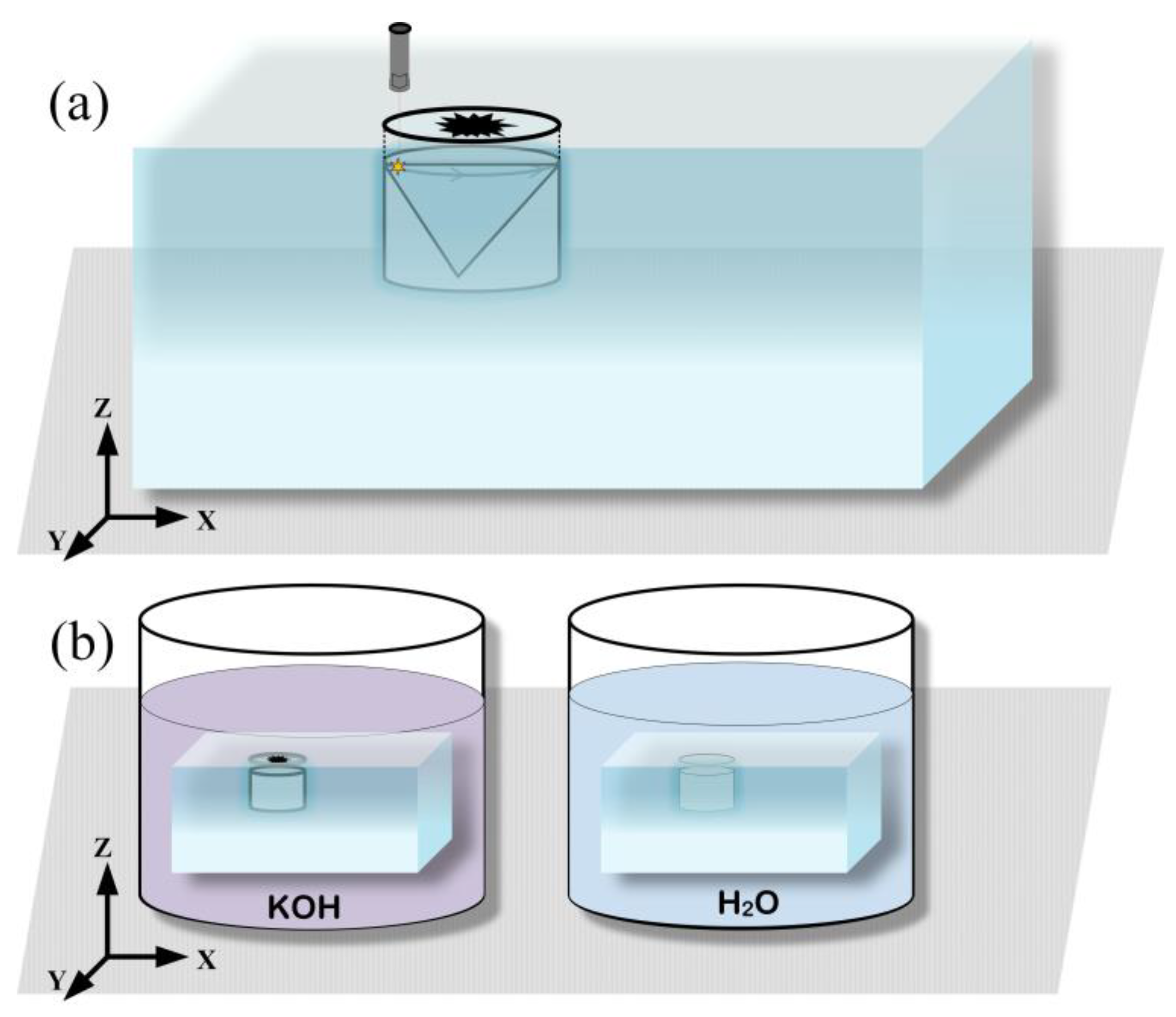
The schematic diagram of the whole repair process is shown in
Figure 1. The wavelength of the femtosecond laser is 1030 nm, the pulse width of 290 fs, and the repetition frequency range of 50 kHz to 500 kHz. The fused silica sample is polished on four sides, which is convenient for observing the modification and etching effect from the side. The geometric dimensions are 4 mm × 6 mm × 50 mm. The femtosecond laser was focused into the sample using a microscope objective. The samples were placed on a high-precision XY plane displacement table, and the microscope objective for focusing moved along the Z-axis. Thus, the three-dimensional scanning of femtosecond laser inside the sample was realized using the plane motion of the sample and the vertical motion of femtosecond laser. In this way, the material around the damage point of the sample could be modified by irradiation. After the modification, the sample was immersed in a potassium hydroxide solution to etch the modified materials. Finally, the samples were washed with alcohol and ultrapure water.
The influence of the femtosecond laser parameters, displacement system parameters, and etching solution ratio was studied. In the course of the experiment, the comparison of samples morphology was taken using an optical microscope (5X, 50X) and a laser confocal microscope. The optical microscope observes the surface morphology. The laser confocal microscope can conduct nondestructive scanning imaging of three-dimensional structures, which is more conducive to observing the etching depth, material morphology changes, and so on. The potassium hydroxide solution with a mass fraction of 58% was used for etching, and the commonly used hydrofluoric acid solution with a mass fraction of 5% was used as the control group. The samples were ultrasonically cleaned with alcohol, acetone, and ultrapure water after etching. The etching rate of the substrate was obtained by comparing the weight of the unmodified fused silica sample before and after etching. It was found that the etching rate in the hydrofluoric acid solution and the potassium hydroxide solution was about 2 μm/h and 1 μm/h, respectively. This is less than one-thousandth of the thickness of the substrate material, so it can be ignored.
3. Results and Discussion
3.1. The Femtosecond Laser Modification Repair of Damage Point
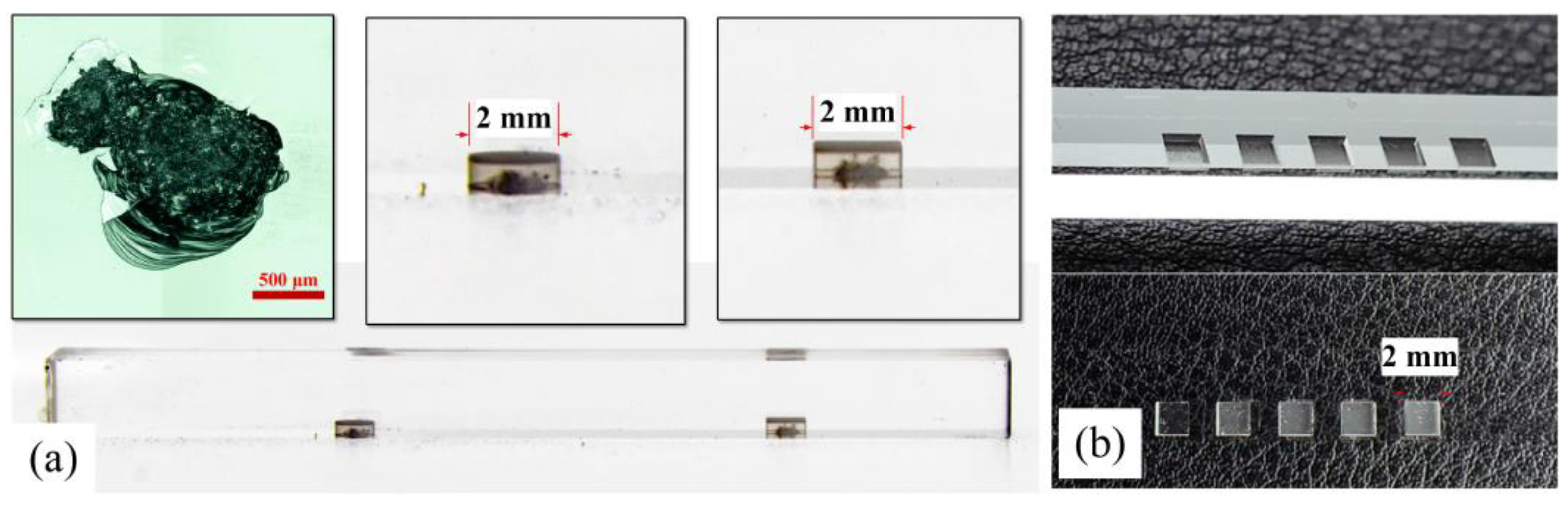
The damage points of the fused silica had been modified and etched as shown in
Figure 2. The morphology of a typical damage point is shown in the insets of
Figure 2a. The top view shows that its horizontal dimension is about 1.5 mm, and the side view shows that its depth is about hundreds of microns. It is an irregular pit with some cracks around it. These damage points on the optical components were irreversible. At present, the general method is to remove the materials around it to prevent it from expanding rapidly. We proposed repairing the damage points using selective femtosecond laser-induced etching. The rest of
Figure 1a shows the modified fused silica, which is the first step of the repair process. Here, we show two typical examples. It can be found that each damage point is surrounded by a hollow geometry, which is translucent. These were formed by the scanning track of the femtosecond laser focus in modification. The middle cylinder has a circle radius of 1 mm and a height of 500 μm. The right rectangle has a side length of 2 mm and a height of 500 μm. This means that different modification trajectories can be preset according to the size and shape of the damage point.
Figure 2b shows the fused silica that had been etched. It could be found that the damage point had been successfully removed from the substrate.
3.2. Femtosecond Laser Parameters
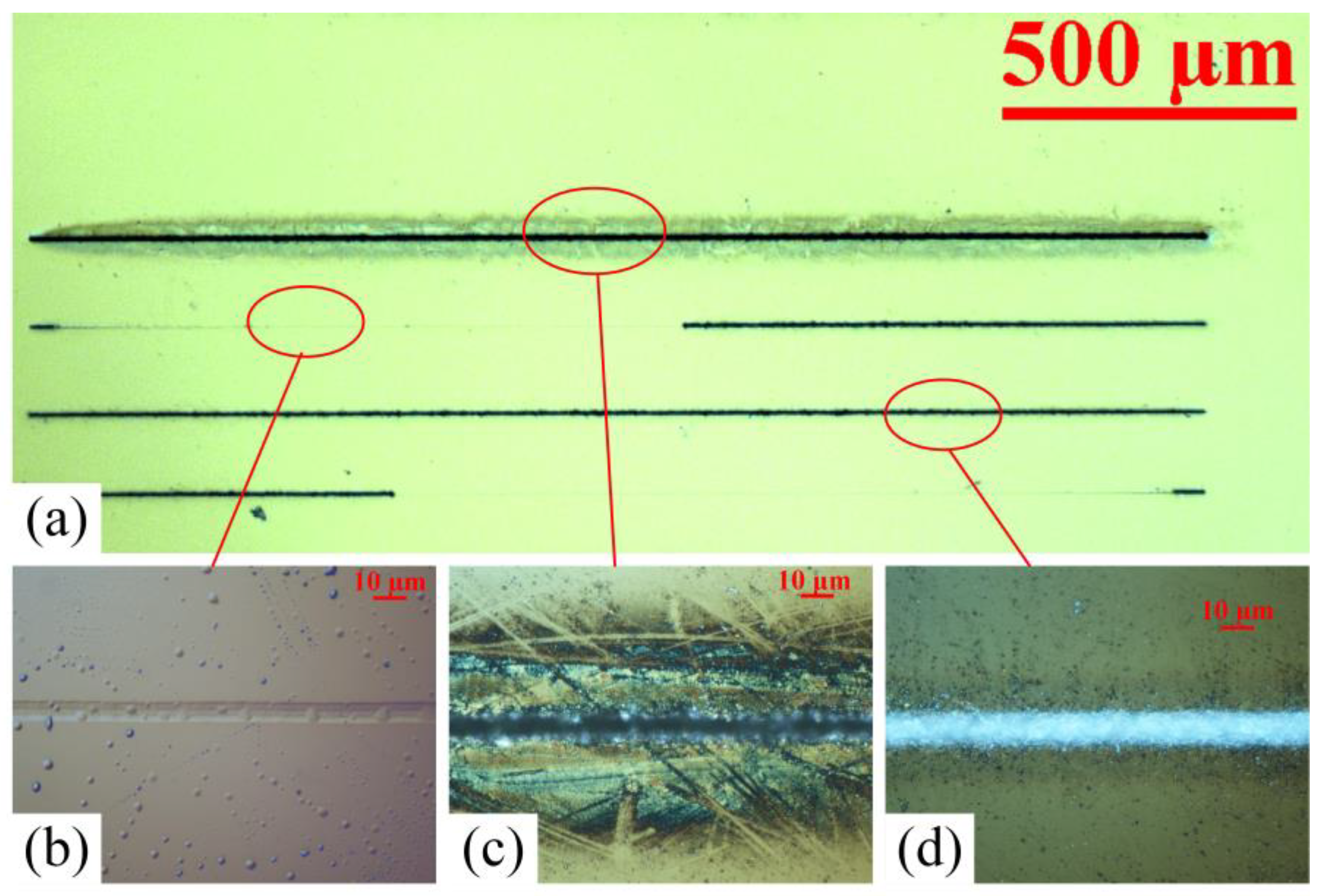
In this experiment, the wavelength of the femtosecond laser is 1030 nm, the energy variation range of a single pulse is 1 μJ to 10 μJ, and the repetition frequency range is 50 kHz to 500 kHz. We scan the line on the surface of fused silica at a constant speed (10 mm/s). The line is 2 mm long and about 10 μm wide. The fused silica after scanning at varied levels of single pulse energy and repeat frequencies of the femtosecond laser are shown in
Figure 3. The scanning lines of various parameters were obviously different. It is found that when the single pulse energy was low (<2 μJ) or the repetition frequency was small (<100 kHz), there was a slight trace of modification on the sample, as shown in the microscope picture of
Figure 3b. On the contrary, when the laser single pulse energy is too high (>10 μJ), the fused silica was ablated with violent splashing, as shown in
Figure 3c. These results show that for the given scanning speed, the modification of fused silica is possible only for the single pulse energy and repeat frequency within a certain range; furthermore, the highest laser flux for modification corresponds to the optimum processing speed.
Figure 3d shows the microscope photos of the uniform modification effect when the single pulse energy is approximately 5 μJ and the repetition frequency is 200 kHz. It can be clearly seen that the modified part shows brighter colors than the surrounding area, and it is a continuous scanning line with uniform line width. There were a few splashing attachments on both sides. After many experiments, it is confirmed that the modification of fused silica occurs when the laser parameters are in an appropriate range. The single pulse energy is approximately 2 μJ to 5 μJ, and the repetition frequency is approximately 200 kHz to 500 kHz.
3.3. Scanning Speed in Modification
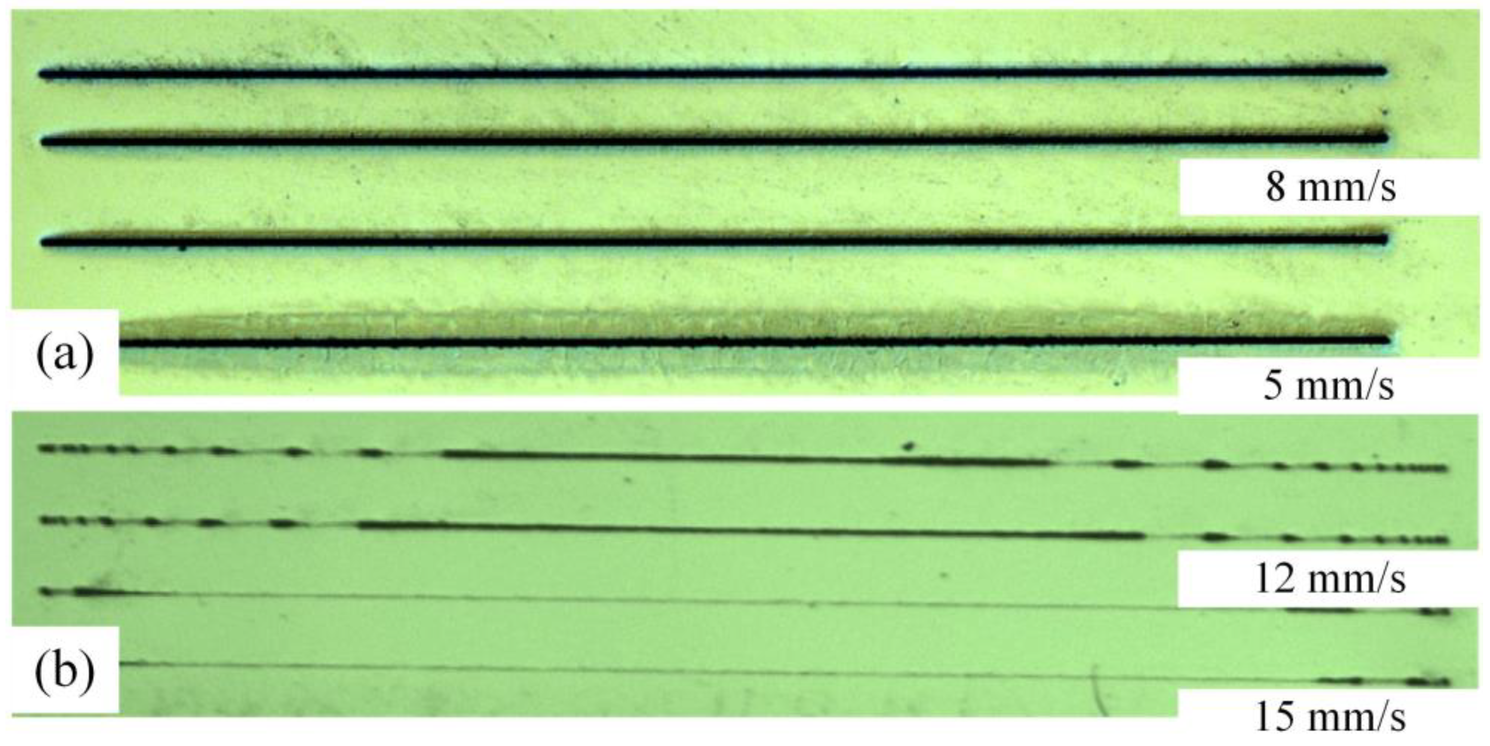
The scanning speed is adjusted by the three-dimensional motion platform. Laser scanning speed was a key factor in judging the efficiency of the sample modification. In order to study the effect of the laser scanning speed on the modification effect of fused silica, the modified lines were set at different scanning speeds when the laser single pulse energy was 5 μJ and the repetition rate is 200 kHz. The effect of scanning speed on sample modification efficiency was obtained by observing and comparing the modification effect of samples obtained using different parameter combinations.
Figure 4 shows the modified morphology obtained using different parameter combinations. As shown in
Figure 4, when the scanning speed is less than 10 mm/s, the surface roughness and the edge collapse around the scanning line will increase as the scanning speed decreases. This is because when the scribing speed is low, the energy per unit area irradiated by the laser pulse on the surface of the material is high, which easily causes ablation and melting, the heat affected area is large, and there are many splashes, as shown in
Figure 4a. When the scanning speed is 10 mm/s, the section roughness and the edge collapse of the glass reach the minimum, as shown in
Figure 3c. When the speed is greater than 10 mm/s, the energy radiated by the laser pulse on the unit area of the material surface is low, resulting in the discontinuity of the scanning line area, as shown in
Figure 4b.
3.4. Etching Solution
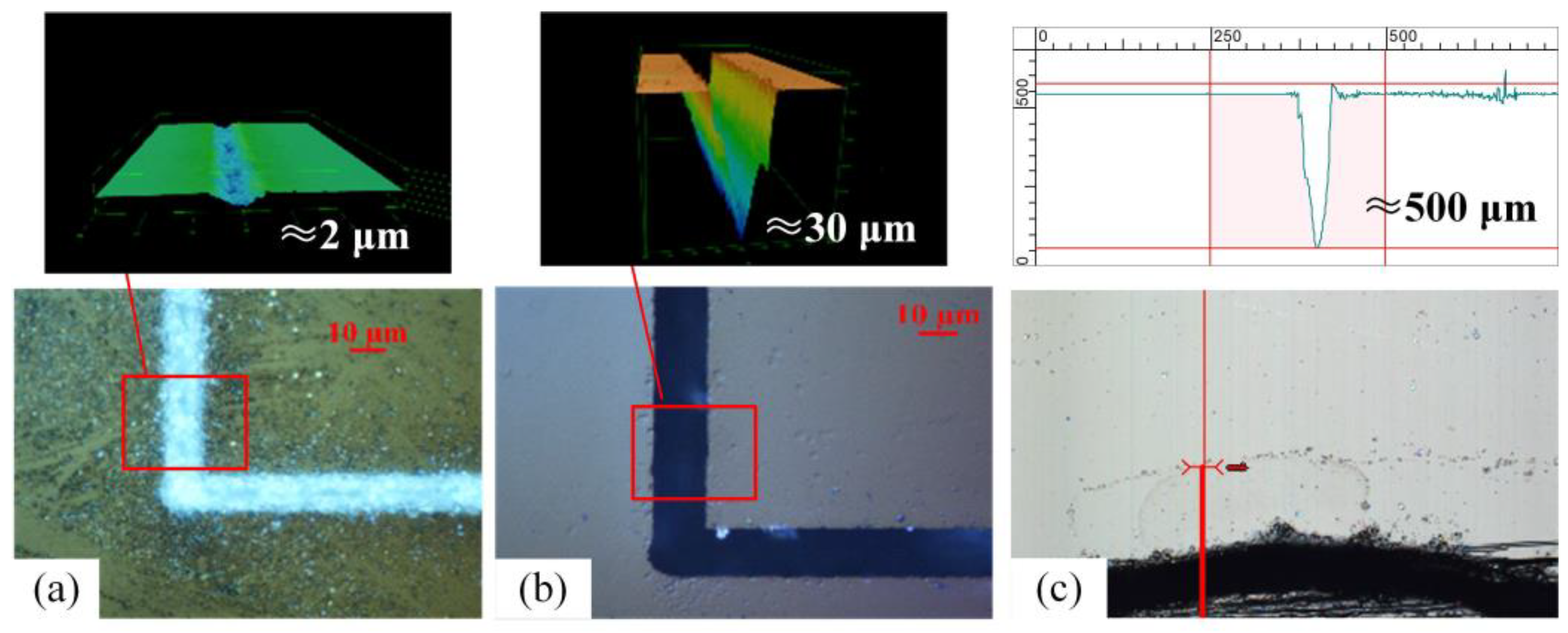
The fused silica samples were modified with the optimized femtosecond laser parameters and scanning speed. Then the modified samples were etched with hydrofluoric acid and potassium hydroxide solutions, respectively, and their etching rates were compared and analyzed. The top view and three-dimensional morphology of the sample before etching are shown in
Figure 5a. The modified track is distributed along the femtosecond laser scanning line. There are molten splashes around the modified area, and the initial depth of the modified area is about 2 μm. It presents a bright optical waveguide under the illumination of the optical microscope. There are some fine particles with the same color beside that area, which seem to pollute the surface of the substrate. The top view and three-dimensional morphology of the sample after etching by hydrofluoric acid are shown in
Figure 5b. We found that the modified material had been completely etched, and the nearby fine particles were also taken away. The depth of the modified area was about 30 μm after etching with hydrofluoric acid, and 500 μm when etched with the potassium hydroxide solution, as shown in
Figure 5c.
4. Conclusions
In this paper, a composite repair method of femtosecond laser three-dimensional modification combined with alkali selective etching is proposed, providing a new and efficient way to repair the damaged points of fused silica. The femtosecond laser selective etching technology is applied to repair the damaged points on the surface of fused silica, and the materials around the damaged points are modified with relatively small femtosecond laser energy, instead of being directly ablated by the carbon dioxide laser, so as to avoid microcrack damage to the substrate materials. 3D contour scanning is used instead of point-by-point scanning, which greatly reduces the workload and heat accumulation during laser scanning and maximizes the modification effect to achieve high repair efficiency. We chose a safer potassium hydroxide etching solution that has a higher etching selection ratio and homogenization effect on the interface of the repaired area. Through femtosecond laser selective etching technology, the material in the damaged area is removed, and the femtosecond laser repair of the damaged point of fused silica is realized. The influence of femtosecond laser single pulse energy, repetition frequency, and scanning speed on the modification effect of fused silica was analyzed, and the etching rate of modified fused silica using a hydrofluoric acid solution and a potassium hydroxide solution was compared. The relevant results have reference significance for the repair of fused silica damage and machining of hard and brittle materials. In the future, we will focus on optimizing the shape of the repair track with this method to further improve the repair efficiency, to increase the damage threshold, and to reduce the impact of the repairing on the optical performance of the original element.
Author Contributions
Conceptualization, W.L. and Z.F.; Formal analysis, L.Z.; Investigation, J.W., H.W. and Q.W.; Methodology, Z.F., J.C. and C.Z.; Resources, X.L.; Visualization, X.J.; Writing—original draft, Z.F.; Writing—review & editing, Z.F. All authors have read and agreed to the published version of the manuscript.
Funding
This research was funded by National Natural Science Foundation of China, Grant No. 12275254 & 62275235; Youth Program of National Natural Science Foundation of China, Grant No. 61804145.
Conflicts of Interest
The authors declare no conflict of interest. The funders had no role in the design of the study; in the collection, analyses, or interpretation of data; in the writing of the manuscript, or in the decision to publish the results.
References
- Zhang, C.; Zhang, L.; Jiang, X.; Jia, B.; Liao, W.; Dai, R.; Chen, J.; Yuan, X. Influence of pulse length on heat affected zones of evaporatively-mitigated damages of fused silica optics by CO2 laser. Opt. Lasers Eng. 2019, 125, 105857. [Google Scholar] [CrossRef]
- Li, Z.; Kong, X.; Zhang, J.; Shao, L.; Zhang, D.; Liu, J.; Wang, X.; Zhu, W.; Qiu, C. Cryptography Metasurface for One-Time-Pad Encryption and Massive Data Storage. Laser Photon-Rev. 2022, 16, 2200113. [Google Scholar] [CrossRef]
- Nasiri, S.; Khosravani, M.R. Applications of data-driven approaches in prediction of fatigue and fracture. Mater. Today Commun. 2022, 33, 104437. [Google Scholar] [CrossRef]
- Zhang, L.; Wang, X.; Lu, S.; Jiang, X.; Ma, C.; Lin, L.; Wang, X. Fatigue damage monitoring of repaired composite wind turbine blades using high-stability bucky paper sensors. Compos. Sci. Technol. 2022, 227, 109592. [Google Scholar] [CrossRef]
- Doualle, T.; Gallais, L.; Monneret, S.; Bouillet, S.; Bourgeade, A.; Ameil, C.; Lamaignère, L.; Cormont, P. CO2 laser microprocessing for laser damage growth mitigation of fused silica optics. Opt. Eng. 2016, 56, 011022. [Google Scholar] [CrossRef]
- Bass, I.L.; Guss, G.M.; Nostrand, M.J.; Wegner, P.J. An improved method of mitigating laser-induced surface damage growth in fused silica using a rastered pulsed CO2 laser. In Laser-Induced Damage in Optical Materials; SPIE Laser Damage: Boulder, CO, USA, 2010; Volume 784, pp. 522–533. [Google Scholar]
- Zhang, C.-C.; Zhang, L.-J.; Liao, W.; Yan, Z.-H.; Chen, J.; Jiang, Y.-L.; Wang, H.-J.; Luan, X.-Y.; Ye, Y.-Y.; Zheng, W.-G.; et al. ATR-FTIR spectroscopic studies on density changes of fused silica induced by localized CO 2 laser treatment. Chin. Phys. B 2015, 24, 024220. [Google Scholar] [CrossRef]
- Cheng, J.; Yang, Z.; Wang, C.; Zhao, L.; Chen, M.; Wang, J.; Li, Y.; Xu, Q.; Liu, Z.; Xu, H. Effect of scratches on the damage characteristics of fused silica optics under extremely-high impact load. Int. J. Mech. Sci. 2022, 219, 107099. [Google Scholar] [CrossRef]
- Lin, Y.; Jiang, Y.; Wei, H.; Fan, W.; Li, X. Research on damage repair of dielectric film based on femtosecond laser micromachining. Acta Phys. Sin. 2015, 64, 0154207. [Google Scholar] [CrossRef]
- Fang, Z.; Zhao, Y.; Chen, S.; Hu, G.; Liu, W.; Chen, W.; Li, D.; Shao, J. Femtosecond laser repair technology for ultraviolet damage points on fused silica surface. Chin. Laser 2013, 40, 0403001. [Google Scholar] [CrossRef]
- Juodkazis, S.; Nishimura, K.; Misawa, H.; Ebisui, T.; Waki, R.; Matsuo, S.; Okada, T. Control over the Crystalline State of Sapphire. Adv. Mater. 2006, 18, 1361–1364. [Google Scholar] [CrossRef]
- Gottmann, J.; Hermans, M.; Ortmann, J. Microcutting and hollow 3D microstructures in glasses by in-volume selective laser-induced etching (ISLE). J. Laser Micro Nanoeng. 2013, 8, 15. [Google Scholar] [CrossRef]
- Rennpferdt, L.; Bohne, S.; Trieu, H.K. Advances in manufacturing spinal cord implant using 3D selective laser induced etching of fused silica. Trans. Addit. Manuf. Meets Med. 2021, 3, 574. [Google Scholar]
- Wang, W.; Li, Z.; Yao, P.; Li, J.; Chen, F.; Liu, Y. Sink-in/pile-up formation and crack nucleation mechanisms of high purity fused silica and soda-lime silica glass during nanoindentation experiments. Ceram. Int. 2020, 46, 24698–24709. [Google Scholar] [CrossRef]
- Chen, J.; Lu, X.; Wen, Q.; Jiang, F.; Lu, J.; Lei, D.; Pan, Y. Review on laser-induced etching processing technology for transparent hard and brittle materials. Int. J. Adv. Manuf. Technol. 2021, 117, 2545–2564. [Google Scholar] [CrossRef]
- Matsuo, S.; Shichijo, Y.; Tomita, T.; Hashimoto, S. Laser fabrication of ship-in-a-bottle microstructures in sapphire. JLMN 2007, 2, 114–116. [Google Scholar] [CrossRef]
- Huang, J.; Fu, X.; Liu, G.; Xu, S.; Li, X.; Zhang, C.; Jiang, L. Micro/nano-structures-enhanced triboelectric nanogenerators by femtosecond laser direct writing. Nano Energy 2019, 62, 638–644. [Google Scholar] [CrossRef]
- Ali, M.; Wagner, T.; Shakoor, M.; Molian, P.A. Review of laser nanomachining. J. Laser Appl. 2008, 20, 169–184. [Google Scholar] [CrossRef]
- Wolfe, J.E.; Qiu, S.R.; Stolz, C.J. Fabrication of mitigation pits for improving laser damage resistance in dielectric mirrors by femtosecond laser machining. Appl. Opt. 2011, 50, C457–C462. [Google Scholar] [CrossRef]
- Liao, K.; Wang, W.; Mei, X.; Liu, B. Research on femtosecond laser single-shot high-quality direct cutting of thin quartz glass based on filament effect (invited). Acta Photonica Sin. 2021, 50, 3. [Google Scholar]
- Zha, H.; Yao, Y.; Wang, M.; Chen, N.-K.; Zhang, L.; Bai, C.; Liu, T.; Ren, Y.; Jia, Y. Bending 90° Waveguides in Nd:YAG Crystal Fabricated by a Combination of Femtosecond Laser Inscription and Precise Diamond Blade Dicing. Crystals 2023, 13, 188. [Google Scholar] [CrossRef]
- Gamaly, E.G.; Rode, A.; Luther-Davies, B.; Tikhonchuk, V.T. Ablation of solids by femtosecond lasers: Ablation mechanism and ablation thresholds for metals and dielectrics. Phys. Plasmas 2002, 9, 949–957. [Google Scholar] [CrossRef]
- Jeschke, H.O.; Garcia, M.E.; Bennemann, K.H. Theory for the Ultrafast Ablation of Graphite Films. Phys. Rev. Lett. 2001, 87, 015003. [Google Scholar] [CrossRef] [Green Version]
- Lenzner, M.; Krüger, J.; Sartania, S.; Cheng, Z.; Spielmann, C.; Mourou, G.; Kautek, W.; Krausz, F. Femtosecond Optical Breakdown in Dielectrics. Phys. Rev. Lett. 1998, 80, 4076–4079. [Google Scholar] [CrossRef]
- Du, D.; Liu, X.; Korn, G.; Squier, J.; Mourou, G. Laser-induced breakdown by impact ionization in SiO2 with pulse widths from 7 ns to 150 fs. Appl. Phys. Lett. 1994, 64, 3071–3073. [Google Scholar] [CrossRef]
- Matsuo, S.; Sumi, H.; Kiyama, S.; Tomita, T.; Hashimoto, S. Femtosecond laser-assisted etching of Pyrex glass with aqueous solution of KOH. Appl. Surf. Sci. 2009, 255, 9758–9760. [Google Scholar] [CrossRef]
- Gorelik, T.; Will, M.; Nolte, S.; Tuennermann, A.; Glatzel, U. Transmission electron microscopy studies of femtosecond laser induced modifications in quartz. Appl. Phys. A 2003, 76, 309–311. [Google Scholar] [CrossRef]
- Nakashima, S.; Sugioka, K.; Midorikawa, K. Fabrication of microchannels in single-crystal GaN by wet-chemical-assisted femtosecond-laser ablation. Appl. Surf. Sci. 2009, 255, 9770–9774. [Google Scholar] [CrossRef]
- Wortmann, D.; Gottmann, J.; Brandt, N.; Horn-Solle, H. Micro- and nanostructures inside sapphire by fs-laser irradiation and selective etching. Opt. Express 2008, 16, 1517–1522. [Google Scholar] [CrossRef]
- Kiyama, S.; Matsuo, S.; Hashimoto, S.; Morihira, Y. Examination of Etching Agent and Etching Mechanism on Femotosecond Laser Microfabrication of Channels Inside Vitreous Silica Substrates. J. Phys. Chem. C 2009, 113, 11560–11566. [Google Scholar] [CrossRef]
- Sinha, A.; Gupta, M.C. Microscale patterning of semiconductor c-Si by selective laser-heating induced KOH etching. Semicond. Sci. Technol. 2021, 36, 085002. [Google Scholar] [CrossRef]
| Disclaimer/Publisher’s Note: The statements, opinions and data contained in all publications are solely those of the individual author(s) and contributor(s) and not of MDPI and/or the editor(s). MDPI and/or the editor(s) disclaim responsibility for any injury to people or property resulting from any ideas, methods, instructions or products referred to in the content. |
© 2023 by the authors. Licensee MDPI, Basel, Switzerland. This article is an open access article distributed under the terms and conditions of the Creative Commons Attribution (CC BY) license (https://creativecommons.org/licenses/by/4.0/).


