Article

Reactive Spark Plasma Sintering and Thermoelectric Properties of Zintl Semiconducting Ca14Si19 Compound

1
Institut Laue-Langevin (ILL), 38042 Grenoble, France
2
ICGM, Univ. Montpellier, CNRS, ENSCM, Montpellier, France
3
ICMPE-CNRS, Univ. Paris-Est Creteil, 94320 Thiais, France
4
CIRIMAT, Université de Toulouse, CNRS, Université Paul-Sabatier, 118 Route de Narbonne, CEDEX 9, 31062 Toulouse, France
*
Authors to whom correspondence should be addressed.
Crystals 2023, 13(2), 262; https://doi.org/10.3390/cryst13020262
Submission received: 2 December 2022 / Revised: 6 January 2023 / Accepted: 25 January 2023 / Published: 2 February 2023
(This article belongs to the Special Issue Recent Developments of Inorganic Crystalline Materials)

Abstract

:
We present a new reactive spark plasma sintering (RSPS) technique for synthesizing the rhombohedral Ca 14 Si 19 phase. The RSPS approach reduces the synthesis time from several weeks to a few minutes. The RSPS was found to be sufficient for obtaining a high level of purity of the Ca 14 Si 19 under a pressure of 100 MPa for a dwell period of 5 min at a temperature of 900 C. From electrical resistivity measurements, we were able to determine the energy band gap of Ca 14 Si 19 to E g = 0.145 ( 15 ) eV. The Seebeck coefficient shows Ca 14 Si 19 as a p-type semiconductor at room temperature. It becomes n-type with increasing temperature pointing to significant bipolar and conduction band contributions due to the narrow bandgap of the compound.

1. Introduction

The development of all modern societies significantly relies on energy sources. Consequently, global energy demand is one of the most significant challenges in the 21st century. It contributes significantly to economic, social, and geopolitical instabilities. Furthermore, the use of limited energy sources, such as fissile or fossil fuels (oil, gas, coal, etc.), are associated, respectively, with long-term radioactive contamination or environmental crises such as global climate change and global warming induced by CO 2 emissions. However, these limited energy sources currently provide around 85% of energy supply [1,2]. Therefore, providing a reliable supply of clean, affordable energy is always in high demand. Numerous alternative energy sources, including photovoltaic, wind, geothermal, and thermoelectrics have received particular attention in the last decade. It is known since the nineteenth century that thermoelectric materials (TEMs) are able to convert thermal heat into electricity via Seebeck’s effect [3] and vice versa via Peltier’s effect [4]. Seebeck’s effect attracts high interest for its potential to generate electrical power from waste heat. Therefore, it is expected to significantly contribute to the world’s future electrical power management and economy by harvesting waste heat released in industry, transport, and household applications [5,6]. Moreover, thermoelectric modules have many advantages such as the absence of movable elements or cryogenic fluids, compactness, higher reliability, and overall life expectancy. However, the efficiency of thermoelectric modules is much lower than those of conventional electrical power generators with mechanical parts [7]. Indeed, the efficiency of thermoelectric devices is limited to about 10% compared to 30% of modern steam turbines [7]. Thus, the performance of TEMs still requires a significant boost.
Thermoelectric modules are made of two legs made of p-type and n-type materials connected electrically in serial and thermally in parallel. Therefore, both p-type and n-type TEMs must be optimized. Their efficiency is related to the thermoelectric dimensionless figure of merit ( Z T ) defined in Equation (1) as
Z T = S 2 ρ ( k e + k l ) T
with the Seebeck coefficient S, electrical resistivity ρ , absolute temperature T, and the electronic and lattice thermal conductivities k e and k l , respectively [8]. Equation (1) clearly underlines that a high power factor S 2 / ρ and low thermal conductivities k e and k l are the key features for high Z T numbers. Thereby the parameters k e and S 2 / ρ are bound by electronic conditions placing TEMs into the regime of semiconductors and semi-metals.
Most of the best TEMs and notably Bi 2 Te 3 and PbTe are semiconducting materials with narrow energy bandgaps smaller than 0.5 eV, allowing for a Z T higher than 1 [6]. The optimal charge carrier concentration for optimizing these types of materials is in the 10 19 –10 20 cm 3 range [9], although some poor metals with both a highly dispersive band and a flat band, such as filled skutterudites, can also have large power factors [10]. Another way of improving the power factor is to lower the dimensionality of the TEMs. Lattice thermal conductivity can be reduced in different ways. Following Glenn Slack, excellent thermoelectric performance can be achieved in materials by respecting the electron crystal and phonon glass concept [11]. Semiconducting compounds with complex crystal structures made of a high number (N) of atoms per primitive unit cell meet this concept closely. Since the main carriers of the heat are acoustic phonons, however, they represent, only 1/N of the total vibrational spectrum in such complex compounds. Moreover, high structural complexity often leads to reduced phonon velocities as well as to high phonon-phonon scattering due to strong interactions of acoustic with low-energy optical modes [11,12,13,14]. This effect can be particularly well triggered by alloying TEMs with heavy elements. Other sources of enhanced phonon scattering can be static in nature such as defects, dopants, or interfaces in nanostructured materials.
The majority of today’s best-performing and purchasable TEMs are made from rare [15], hence expensive, and often toxic chemical elements [9,16,17,18,19]. Alkaline-earth silicide compounds offer a unique opportunity to overcome these cost and hazard issues. As an example, calcium silicides are made up of the fifth (Ca) and second (Si) most abundant elements in the earth’s crust [15,20]. Hence, they are cheap, and additionally, they are non-toxic. As many of the calcium silicide compounds are equally semiconducting and have a complex crystal structure, they fulfill all necessary requirements to become the next generation of environment-friendly TEMs.
Only a few alkaline-earth silicides have been investigated for their TEM capability. As far as we know, the calcium–silicide family consists of six members in the equilibrium phase diagram: orthorhombic CaSi [Cmcm, No 63], rhombohedral CaSi 2 [R-3m, No 166], tetragonal Ca 5 Si 3 [I4/mcm, No 140], orthorhombic Ca 2 Si [Pnma, No 62], hexagonal Ca 3 Si 4 [P6 3 /m, No 176], and rhombohedral Ca 14 Si 19 [R-3c, No 167] [21,22,23,24,25,26,27,28,29,30]. In addition to the stable R6 rhombohedral CaSi 2 phase with 6 layers stacking, there is a metastable R3 rhombohedral CaSi 2 phase [R-3m, No 166] with 3 layers stacking that can be obtained from the sintering of R6 CaSi 2 under H 2 atmosphere or from thin film epitaxial growth [31,32]. The R6 rhombohedral CaSi 2 phase undergoes two structural phase transitions under high pressure and below 700 K, to a trigonal [P-3m1, No 164] phase between 8 and 16 GPa and to a hexagonal phase [P6/mmm, No 191] above 16 GPa [33,34]. Under high-pressure and high-temperature conditions, a tetragonal CaSi 2 phase [I4 1 /amd, No 141] was obtained above 4 GPa [33,34,35]. All the CaSi 2 polymorphs are metallic [31,33,36] and the different high-pressure phases are superconducting at low temperatures [33]. Other Si-rich calcium silicide phases were obtained under high-pressure and high-temperature conditions such as tetragonal CaSi 3 [I4/mmm, No 139] [37] from 12 GPa and orthorhombic CaSi 6 [Cmcm, No 63] [38] at 10 GPa. Both compounds are metallic, the first one being superconducting below 4.5 K [37] whereas the last one is formed of channels where Ca atoms are intercalated [38]. Among all the other calcium silicide compounds, density functional theory (DFT) calculations show that only Ca 2 Si, Ca 3 Si 4 , and Ca 14 Si 19 are semiconducting compounds [28,39,40,41,42]. Orthorhombic Ca 2 Si is semiconductive with a direct energy bandgap of about 0.88 eV, recently reported from optical spectra of a Ca 2 Si thin film on sapphire substrate [32], which is slightly lower than the value of 1.02 eV found with GW calculations, a post-DFT method that corrects the energy bandgap obtained from the DFT method [40]. Growth of thin films has been performed for applications such as light-emitting diodes in the near-infrared range [32]. Thermoelectric and electrical transport experiments on orthorhombic Ca 2 Si [43,44] showed that it is p-type and that the electrical conductivity ( σ ) is too weak, even after doping with Na, and that the energy activation found is much smaller than the energy bandgap found from the optical experiments [32]. Concerning Ca 5 Si 3 , there are several contradicting results. Jun et al. [45] reported an energy bandgap of 0.65 eV from infrared absorption on a badly crystallized thin film of Ca 5 Si 3 , but there was still a strong absorption signal below this energy in their data, which cast doubts about their conclusions. Inaba et al. [46] and Wen et al. [43] both reported an increase in electrical conductivity ( σ ) with temperature, whereas Uhera et al. [47] found an almost independent behavior and Imamura et al. [48] found a decrease of the electrical conductivity ( σ ) at higher temperatures characteristic of metals that is in agreement with DFT calculations [41]. Ca 5 Si 3 is of p-type and its Seebeck coefficient varies from 30 μ V/K to 90 μ V/K, depending on the different works [46,47,48]. Imamura et al. [48] reported a rather large power factor of about 0.6 mWm 1 K 2 and a moderate ZT of 0.11 at 950 K for Ca 5 Si 3 . CaSi and R6 rhombohedral CaSi 2 have Seebeck coefficients of few μ V/K, typical of metals, with a negative sign for CaSi [47,48].
Ca 3 Si 4 and Ca 14 Si 19 are of particular interest as they are semi-conducting valence-charge-balanced Zintl phases with complex crystal structures [39,49]. Ca 3 Si 4 is a low-temperature phase whereas Ca 14 Si 19 is a high-temperature phase, and both phases coexist between 900 C and 930 C [39]. The electronic energy bandgaps were approximated for Ca 3 Si 4 and Ca 14 Si 19 from DFT calculations. Different DFT studies concluded that Ca 3 Si 4 has indirect bandgaps of 0.35 eV [42] and 0.56 eV [39]. The bandgap for Ca 14 Si 19 was found from DFT to be 0.02 eV [39] and experimentally to be 0.12 eV [21]. The Seebeck coefficients of Ca 3 Si 4 and Ca 14 Si 19 at room temperature are 42 μ V/K and −183 V/K, respectively, but the electrical conductivity ( σ ) at room temperature of Ca 3 Si 4 is low [39]. Their thermoelectric properties must be studied in order to conclude their TEM potential. According to the phonon glass electron crystal concept [11,12,13,14], their structural complexity should facilitate low k l values and enhance Z T appreciably. The drawback of the structural complexity is, however, a difficult synthesis process that comprises long-time annealing for several weeks for bulk materials [39], and only very recently thin films containing significant amounts of Ca 14 Si 19 in addition to CaSi 2 have been obtained [32]. As a consequence, while the elements Ca and Si are abundant and cheap, their casting into semiconducting thermoelectric compounds has been tedious, long-lasting, and expensive.
This work aims to pave a new way of synthesizing calcium–silicide compounds. We show a new approach to reduce the time, energy, and thus costs needed to synthesize the rhombohedral Ca 14 Si 19 . This is accomplished by the application of the reactive spark plasma sintering (RSPS) technique [50,51].
Spark plasma sintering (SPS) is an advanced powder metallurgy technique belonging to the family of electrical current-assisted sintering technologies, is a more than 30-year-old advanced sintering process for generating quick powder consolidation–densification, employing a high-intensity pulsed direct current under high uniaxial pressure [50,52]. It became more widespread for the rapid elaboration–densification of all classes of materials (metals, ceramics, and polymers) and their composites because of several advantages over more conventional techniques such as pressureless sintering and hot-pressing, including lower sintering temperatures, higher heating rates, and shorter holding times. This may somehow influence/change the mechanisms involved in the sintering (in densification and/or grain growth stages) of the materials. The development of SPS is still in progress. High-pressure SPS, SP-texturing, and -extrusion have recently been proposed, but the most important progress of the process was achieved with the lifting of one of the technological locks with the development of strategies to develop 3D near-net-shape materials by SPS [53,54]. Sintering involves kinetics and thermodynamics effects; more recently, flash-SPS (with heating rate up to several thousand of C/min) and cold-SPS (densification at a temperature lower than 400 C) have been developed to control the microstructures (grain size, porosity rate, and size, as well as the nature and size of the grain boundaries) of the densified materials [55,56]. Even though specific SPS mechanisms have not been clearly evidenced and generalized, studies have shown that the combination of thermal, electrical, and pressure effects have huge impacts on the structure, the microstructures, and, as a consequence, on the properties of the materials thus obtained. Depending on the nature of the starting material and the technique used, up to three driving forces may be involved to reduce the free energy of the system when conventional sintering occurs: the curvature of the particulate surfaces, externally applied pressure, and chemical reaction [57]. The chemical reaction can be of a different nature (dehydration or decomposition of precursors, reaction of a mixture of elemental or binary compounds, etc.) and may occur during the SPS process which is then RSPS [50,51,58]. This strategy has been applied in particular to sinter refractory materials like borides, carbides, and their composites, or materials of complex compositions such as MAX phases [59] and high-entropy materials [60]. In the case of an exothermic reaction, self-sustained RSPS can achieve an even quicker synthesis, but it is more difficult to manage than conventional RSPS [51]. The utilization of small-sized grains, such as those obtained through ball milling, can improve the reaction in RSPS [50,51,58].
We report a process to form dense Ca 14 Si 19 pellets by combining short-time mechanical milling (5 min) with the RSPS approach. The quality of the synthesis products was followed by X-ray diffraction experiments and the final specimens were characterized for their thermoelectric properties and their hardness. Note that the scope of the discussed RSPS approach can be conveniently extended to synthesize other incongruent phases as previously observed on β -FeSi 2 , while avoiding longtime annealing [58].

2. Material and Methods

2.1. Synthesis of Ca 14 Si 19

High-purity Ca granules (99.5% Alfa Aesar) and Si lumps (99.9999% Alfa Aesar) were used to prepare 0.4–0.5 g of Ca-Si pre-alloy buttons in an arc melting furnace (Welding Concept, France) under an argon atmosphere. The samples’ homogeneity was improved by melting the samples twice. A slight excess of Ca was added to compensate for its evaporation during the melting process. An agate mortar and pestle were used to grind the formed buttons into fine powders. The purest pre-alloy samples obtained from this process were selected by means of X-ray diffraction data. They were sealed under argon in a jar with three 15 mm diameter balls, both made of tungsten carbide. The samples were mechanically milled for 5 min without pauses. We applied a speed of the grinding bowls of ≈740 rpm and a speed of the supporting disc of ≈370 rpm, corresponding to an acceleration speed of ≈5 g in a planetary micro-mill “Pulverisette 7” (Fritsch, Germany).
The reactive spark plasma sintering (RSPS) technique was used to prepare dense pellets using a “Dr Sinter 515S Syntex” machine (Fuji Electronic Industrial Co., Ltd., Japan). Graphite dies (ISO 68 Toyo Tanso) with 8 mm inner diameters were used for these experiments, along with a graphite foil as a protective layer between the sample and the die to increase the lifetime of this latter and for easy removal of the sample. Prior to the experiment, the system was purged with argon gas and the experiment was performed under a primary vacuum (residual cell pressure P = 10 Pa). Uniaxial pressure (100 MPa) was applied at room temperature and all along the thermal cycle and DC pulses were delivered by the graphite punches. The temperature was increased to 900 C at 100 C/min, this temperature was then maintained for a dwell of 5 min. Cooling was applied down to room temperature (100 C/min) and the uniaxial load was gradually released during the same time. The temperature was controlled by a K-type thermocouple incorporated in the mold, close to the sample area. The pattern for the applied pulsed direct current delivered by the SPS machine was a set of 12 consecutive pulses of 3.3 ms each, with a pause of 6.6 ms between pulse sets.

2.2. Sample Characterization

After arc-melting and RSPS treatment, the intermediate and final products were analyzed by X-ray diffraction (X’Pert Pro from Malvern Panalytical in the UK, Cu-K α radiation 1.5406 Å with an accelerated detector PW3050/60 at 45 kV and 30 mA settings). The X-ray data were refined using the Rietveld method with the FullProf software [61]. The chemical homogeneity and composition of the samples were checked using an energy dispersive analyzer of X-ray (EDX) S4800 mounted on an S2600N scanning electron microscope (SEM), both from Hitachi, Japan. Prior to the experiments, the samples were mirror-polished using absolute ethanol as a solvent to avoid surface oxidation. A pellet of diameter 8 mm and thickness 1.456 mm (specimen 1) with a Ca 14 Si 19 content of weight percentage ∼89% was selected for measurements of the electrical resistivity ρ [62], and Seebeck coefficient [63] in the temperature range 325 to 650 K. We used homemade equipment, working under vacuum conditions (≈ 2 . 10 3 mbar) for both experiments. The Van der Pauw method was chosen for the ρ measurements [62]. The pellet’s macroscopic density was determined with Archimedes’ method by measuring both the mass of the pellet in the air and in absolute ethanol. Each sample was measured 10 times for statistics and it was then compared with the microscopic density obtained by the Rietveld refinement. Vickers micro-hardness experiments were performed on a small piece from a pellet (specimen 2) with Ca 14 Si 19 content of weight percentage ∼98% (see below for details) by using a micro-hardness testing machine HM-220 (Mitutoyo, Japan) with two different 0.1 and 0.2 kg loads applied during 10 s. In each case and for both faces of the sample, 10 measurements were performed and the average value is reported in GPa.

3. Results and Discussion

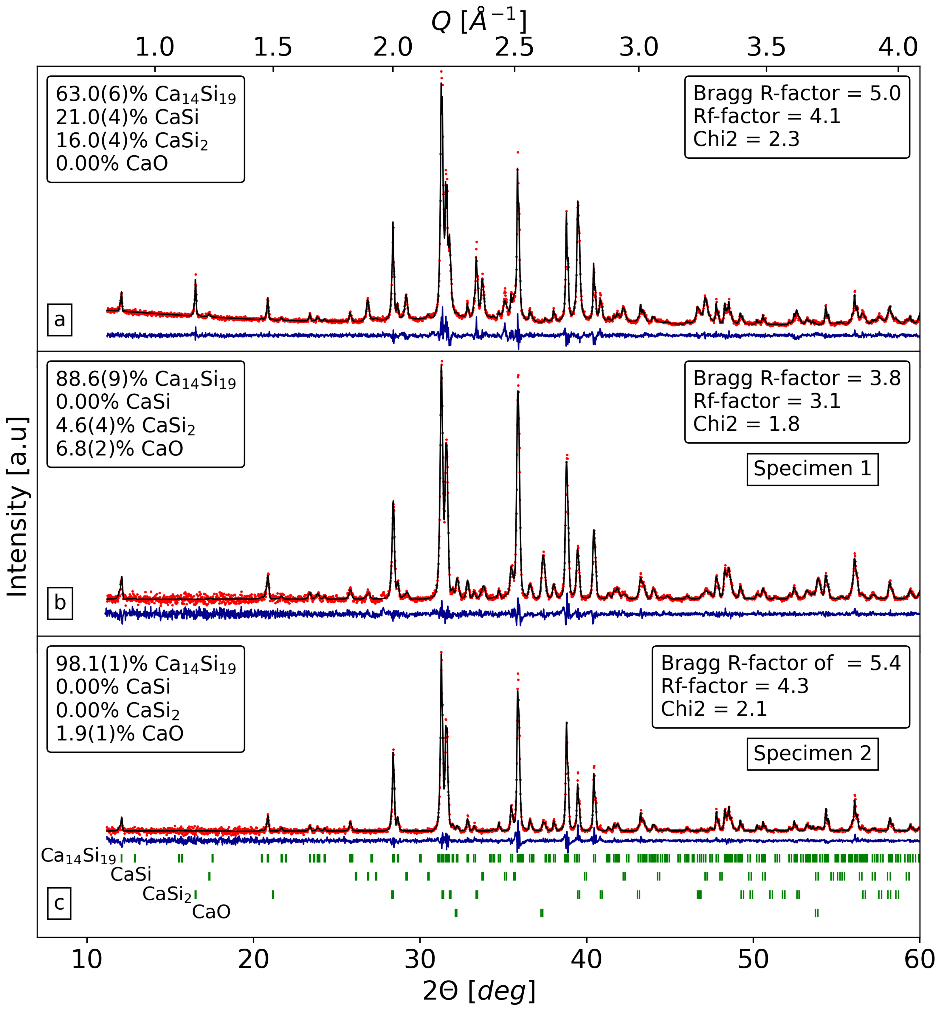
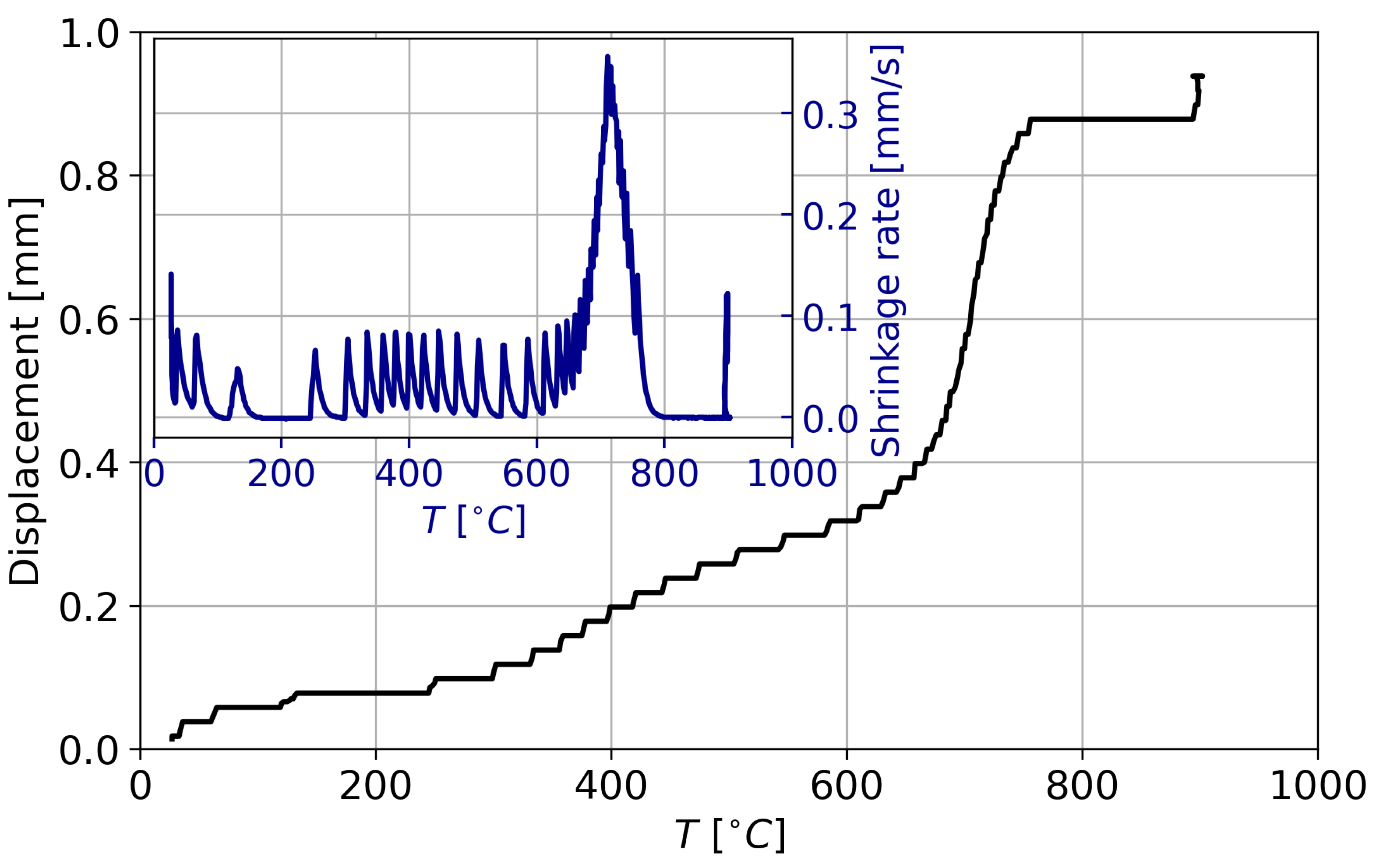
3.1. Sintering Process and Phase Stability of Ca 14 Si 19

A large amount of Ca 14 Si 19 was obtained after arc melting; however, significant percentages of secondary phases such as CaSi and CaSi 2 were also detected. Figure 1a shows a typical X-ray pattern on a powdered sample immediately after arc melting. The weight fractions of Ca 14 Si 19 , CaSi, and CaSi 2 were 0.630, 0.210, and 0.160, respectively. Figure 1b shows an X-ray pattern on the pellet of specimen 1 immediately after RSPS with no CaSi detected. The weight fraction of CaSi 2 was reduced to 0.046, but a small quantity of CaO phase appeared with a weight fraction of 0.068. Despite our efforts, it was not possible to obtain oxygen-free samples. The sintering displacement curve of specimen 1 is given in Figure 2, with data recorded every second. From Figure 2, we observe a slight shrinkage between 250 C and 650 C and a much higher shrinkage between 650 C and 750 C. We conjecture that the shrinkage between 250 C and 650 C could be due to granular rearrangement and that the sintering occurs mainly in the shrinkage between 650 C and 750 C where the shrinkage rate is the largest (0.35 mm/s at 711 C). Dwelling at a temperature of 900 C was chosen to complete the reaction. This temperature is far below the peritectic transition at 1085 C, in which Ca 14 Si 19 decomposes into CaSi and a liquid phase. Note that pellets with high Ca 14 Si 19 content proved to be somewhat brittle. In some RSPS runs we formed pellets with a Ca 14 Si 19 purity higher than weight percentage 98% as shown in the X-ray pattern on the pellet of specimen 2 in Figure 1c. Those pellets broke after extraction from the mold due to residual stresses, which are a consequence of rapidly decreasing temperature, and their brittle nature.
The macroscopic density of the pellets was found to be >99% of the microscopic density. The SEM picture in Figure 3 shows little black regions corresponding to pores in the pellets, confirming their high density. The presence of white spots corresponds to tungsten carbide contamination from the mechanical milling process. Their amount is negligible and does not affect the thermoelectric properties. Larger dark regions are also visible. EDX analysis performed found higher Si content in these regions than expected for Ca 14 Si 19 , which is in line with the presence of the secondary phase CaSi 2 in addition to Ca 14 Si 19 . Within the region free of secondary phases, we observe good homogeneity of the 14:19 stoichiometry. From the EDX analysis, we determine the stoichiometry to be Ca 14.08 Si 19 with a standard deviation of less than 0.6%, which is within the accuracy of the experiment.
The Rietveld-fitted lattice parameters of the Ca 14 Si 19 phase in the different specimens are reported in Table 1 and the corresponding fractional positions of the atoms of specimen 2 after the RSPS process are listed in Table 2. The derived lattice parameters are in good agreement with experimental data recorded at room temperature and published in the literature ( a = b = 8.6707 ( 1 ) Å, c = 68.4864 ( 8 ) Å [39]). We attempted to estimate the occupation numbers of the non-equivalent sites in the Ca 14 Si 19 phases. No systematic or noteworthy deviations from the nominal site occupancies were identified.

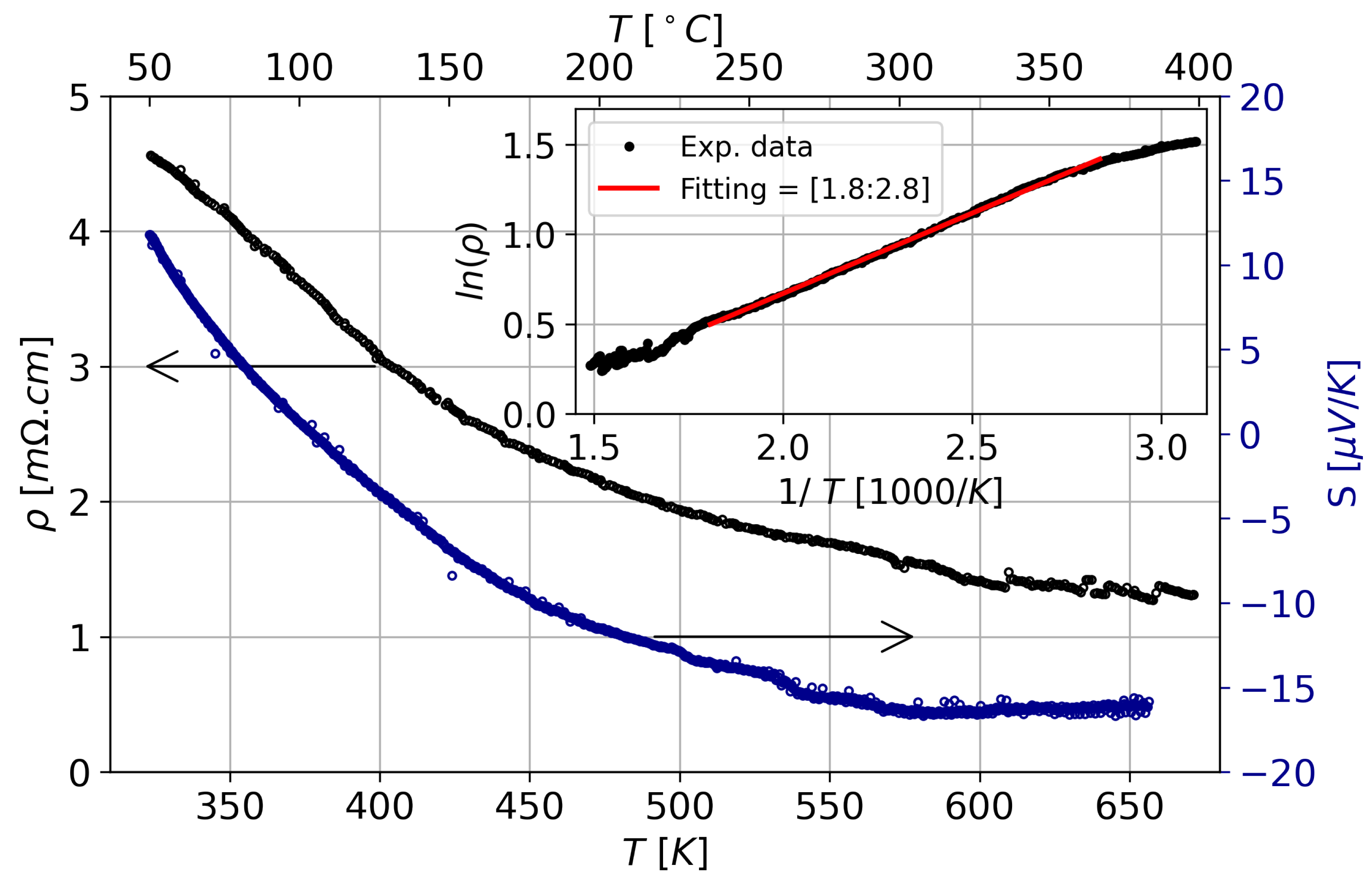
3.2. Thermoelectric and Mechanical Properties

We present results from temperature-dependent measurements of electrical resistivity ( ρ ) and Seebeck coefficient (S) in Figure 4. The electrical resistivity shows a temperature variation characteristic of semiconductors. It decreases from ≈4.5 to ≈1 m Ω · cm upon heating from 50 to 400 C. Assuming a temperature-activated conduction process, we derive from an Arrhenius fit an electronic bandgap of E g = 0.145 ± 0.015 eV, which is in reasonable agreement with the experimental value of 0.12 eV reported in the literature [21]. In prior calculations, we have found that Ca 14 Si 19 has an indirect bandgap with the valence band maximum along the Γ -L line and the conduction band minimum at the X point [39].
As expected from the narrow bandgap, the Seebeck coefficient is small. Interestingly, it changes its sign at about 100 C, decreasing from +12 to −16 μ V/K upon heating. We exclude the possibility that the sign change of the Seebeck coefficient is due to a phase transition or oxidization of the specimen since high-temperature X-ray diffraction experiments performed on Ca 14 Si 19 , obtained by conventional longtime annealing did not reveal any sign of structural changes up to 873 K [64]. We similarly do not expect any significant contribution of the secondary phases in the electrical transport and thermoelectric properties because CaO is an insulator while CaSi 2 is a metal with a low negative Seebeck coefficient of −7 μ V/K that is independent of temperature [47]. In addition, neither of the two phases is present in sufficient quantity to contribute to the electronic transport.
The sign change of the Seebeck coefficient should be due to a significant contribution arising from an increase in the electronic charge carrier minority concentration. Indeed, as Ca 14 Si 19 is a narrow gap semiconductor, let us consider the case of a two-band model, taking into account both conduction and valence bands [65]. In this case, one can express the total electrical conductivity ( σ t o t ) as σ t o t = σ e + σ h , where σ e and σ h are the electrical conductivities from the conduction and valence bands, respectively. Therefore the total Seebeck coefficient (S t o t ) is defined in Equation (2) as [65]
S t o t = σ e S e + σ h S h σ e σ h
with the Seebeck contributions S e and S h from the conduction and valence bands, respectively. As can be seen from the band structure of Ca 14 Si 19 reported by Moll et al. [39], the conduction band is very flat, whereas the valence band is much more dispersive, although being degenerated several times along different directions. Thus, the effective mass of the electrons m e * must be much larger than the effective mass of the holes m h * . Since the larger the effective masses of the charge carrier, the larger the Seebeck coefficient, S e must be much larger than S h . Therefore, when the minority charge carrier concentration increases with the temperature, their electrical conductivity follows as well. In Ca 14 Si 19 , the electrons are the minority charge carriers but have larger Seebeck coefficient S e . Thus, when σ e increases sufficiently with temperature, the sign change of the Seebeck coefficient happens.
However, to reduce the electrical resistivity ( ρ ) and the contribution from minority charge carriers and thus to increase the absolute Seebeck coefficient (S), it will be necessary to dope Ca 14 Si 19 with appropriate elements. Alkaline metals have a low melting point and high partial pressure and their handling is thus challenging within the arc melting furnace used in this synthesis process. Sealed refractory tubes could be employed, which could avoid problems associated with elements boiling off at high temperatures. Such difficulties would not be observed in synthesizing with aluminum or yttrium for p-type and n-type doping, respectively, as these elements have higher melting points and lower partial pressure.
Until now, only a few alkaline-earth silicides have been investigated for their mechanical properties. Vickers hardness has been reported for the two semiconducting silicides Mg 2 Si (4–4.4 GPa) and BaSi 2 (9.11 GPa) [66]. We have determined the Vickers hardness on specimen 2 of Ca 14 Si 19 to be 6.0 ± 0.5 GPa. It is thus located between the values of Mg 2 Si and BaSi 2 [66].

4. Conclusions

Dense Ca 14 Si 19 pellets can be formed from a Ca-Si pre-alloy formed by arc melting followed by combining mechanical milling with the reactive SPS technique. The sintering conditions for obtaining a high level of purity for the Ca 14 Si 19 specimens are 100 MPa at 900 C for a dwell duration of 5 min.
From electrical resistivity ( ρ ) experiments, we have found an electronic energy bandgap that agrees reasonably well with the values previously reported [21]. The Seebeck coefficient (S) for Ca 14 Si 19 indicates the large contribution from the minority charge carriers, which should be due to the narrow bandgap and a large Seebeck of the minority charge carriers. Doping will be necessary to reduce the contribution from the minority charge carriers and to increase both the Seebeck coefficient and the electrical conductivity. Finally, we find that the hardness of Ca 14 Si 19 is about 6 GPa.

Author Contributions

Conceptualization, D.O.A.A., M.M.K., M.B. and R.V.; methodology, D.O.A.A., M.F., C.E.(Claude Estournès), C.E.(Camille Estournès), M.M.K., M.B. and R.V.; formal analysis, D.O.A.A., M.F., C.E.(Claude Estournès), C.E.(Camille Estournès), M.M.K., M.B. and R.V.; investigation, D.O.A.A., L.C., M.F., C.E.(Claude Estournès), C.E.(Camille Estournès), B.V., S.B., M.M.K., M.B. and R.V.; resources, B.V., C.E.(Claude Estournès), L.C., M.B. and R.V.; writing—original draft preparation, D.O.A.A., M.M.K., M.B. and R.V.; writing—review and editing, D.O.A.A., M.M.K., M.B. and R.V.; visualization, M.M.K., M.B. and R.V.; supervision, M.M.K., M.B. and R.V.; project administration, M.M.K., M.B., and R.V.; funding acquisition, M.M.K., M.B. and R.V. All authors have read and agreed to the published version of the manuscript.

Funding

This work was funded by Institut Laue-Langevin (ILL)–71 avenue des Martyrs CS 20156, 38042 GRENOBLE Cedex 9–France.

Data Availability Statement

Original data are available on reasonable request.

Acknowledgments

The authors would like to thank A. Viera E Silva for his technical support and A. Wildes for proofreading the manuscript. Institut Laue-Langevin (ILL), and Institute Charles Gerhardt Montpellier for supporting this project with the required fund and resources.

Conflicts of Interest

The authors declare that they have no known competing financial interests or personal relationships that could have appeared to influence the work reported in this paper.

References

  1. Buchal, C. The challenge of discussing energy facts and climate change. EPJ Web Conf. 2020, 246, 00003. [Google Scholar] [CrossRef]
  2. Kalghatgi, G. Is it really the end of internal combustion engines and petroleum in transport? Appl. Energy 2018, 225, 965–974. [Google Scholar] [CrossRef]
  3. Seebeck, T.J. Magnetische Polarisation der Metalle und Erze durch Temperatur-Differenz; Abhandlungen Der Deutschen Akademie Der Wissenschaften Zu Berlin, 1822–1823; W. Engelmann: Leipzig, Germany, 1895; pp. 265–373. [Google Scholar]
  4. Peltier, J. Nouvelles expériences sur la caloricité des courants électriques. Annal. Chim. Phys. 1834, 56, 371–386. [Google Scholar]
  5. Ong, K.; Jiang, L.; Lai, K. Thermoelectric Energy Conversion; Comprehensive Energy System; Elsevier: Amsterdam, The Netherlands, 2018. [Google Scholar] [CrossRef]
  6. Beretta, D.; Neophytou, N.; Hodges, J.; Kanatzidis, M.; Narducci, D.; Martin-Gonzalez, M.; Beekman, M.; Balke, B.; Cerretti, G.; Tremel, W.; et al. Thermoelectrics: From history, a window to the future. Mater. Sci. Eng. R Rep. 2019, 138, 210–255. [Google Scholar]
  7. Vining, C. An inconvenient truth about thermoelectrics. Nat. Mater. 2009, 8, 83–85. [Google Scholar] [CrossRef]
  8. Ioffe, A. Semiconductor Thermoelements and Thermoelectric Cooling; Infosearch Ltd.: London, UK, 1957. [Google Scholar]
  9. Terasaki, I. Introduction to thermoelectricity. In Materials For Energy Conversion Devices; Woodhead Publishing: Cambridge, UK, 2005; pp. 339–357. [Google Scholar]
  10. Uher, C. Skutterudites: Prospective novel thermoelectrics. Semiconduct. Semimet. 2001, 69, 139–253. [Google Scholar]
  11. Slack, G.A. New Materials and Performance Limits for Thermoelectric Cooling. In CRC Handbook of Thermoelectrics; CRC: Boca Raton, FL, USA, 1995; Chapter 34; pp. 407–440. [Google Scholar]
  12. Takabatake, T.; Suekuni, K.; Nakayama, T.; Kaneshita, E. Phonon-glass electron-crystal thermoelectric clathrates: Experiments and theory. RMP 2014, 86, 669. [Google Scholar] [CrossRef]
  13. Snyder, G.; Toberer, E. Complex thermoelectric materials. Nat. Mater. 2008, 7, 105–114. [Google Scholar] [CrossRef]
  14. Toberer, E.; May, A.; Snyder, G. Zintl chemistry for designing high-efficiency thermoelectric materials. Chem. Mater. 2010, 22, 624–634. [Google Scholar] [CrossRef]
  15. Fleischer, M. The abundance and distribution of the chemical elements in the earth’s crust. J. Chem. Educ. 1954, 31, 446. [Google Scholar] [CrossRef]
  16. Goldsmid, H.; Douglas, R. The use of semiconductors in thermoelectric refrigeration. Br. J. Appl. Phys. 1954, 5, 386. [Google Scholar] [CrossRef]
  17. Bulusu, A.; Walker, D. Review of electronic transport models for thermoelectric materials. Superlattices Microstruct. 2008, 44, 1–36. [Google Scholar] [CrossRef]
  18. Tervo, J.; Manninen, A.; Ilola, R.; Hänninen, H. State-of-the-Art of Thermoelectric Materials Processing; VTT Working Papers: 124; VTT Technical Research Center of Finland: Espoo, Finland, 2009; ISBN 978-951-38-7184-0. [Google Scholar]
  19. Witting, I.; Chasapis, T.; Ricci, F.; Peters, M.; Heinz, N.; Hautier, G.; Snyder, G. The thermoelectric properties of bismuth telluride. Adv. Electron. Mater. 2019, 5, 1800904. [Google Scholar] [CrossRef]
  20. Kuhlmann, A. The second most abundant element in the earth’s crust. JOM 1963, 15, 502–505. [Google Scholar] [CrossRef]
  21. Currao, A.; Wengert, S.; Nesper, R.; Curda, J.; Hillebrecht, H. Ca14Si19—A Zintl Phase with a Novel Twodimensional Silicon Framework. Z. Anorg. Allg. Chem. 1996, 622, 501–508. [Google Scholar] [CrossRef]
  22. Currao, A. Synthese, Struktur und Eigenschaften von Zintlphasen der Erdalkali-und Alkali-Erdalkalimetalle mit Silicium. 1996. Available online: https://www.research-collection.ethz.ch/bitstream/handle/20.500.11850/142715/1/eth-40372-01.pdf (accessed on 1 December 2022).
  23. Manfrinetti, P.; Fornasini, M.; Palenzona, A. The phase diagram of the Ca–Si system. Intermetallics 2000, 8, 223–228. [Google Scholar] [CrossRef]
  24. Canepa, F.; Napoletano, M.; Manfrinetti, P.; Palenzona, A. Heat capacity and thermodynamic properties of some Ca silicides. J. Alloys Compd. 2000, 299, 20–23. [Google Scholar] [CrossRef]
  25. Brutti, S.; Ciccioli, A.; Balducci, G.; Gigli, G.; Manfrinetti, P.; Napoletano, M. Thermodynamic stabilities of intermediate phases in the Ca–Si system. J. Alloys Compd. 2001, 317, 525–531. [Google Scholar] [CrossRef]
  26. Gröbner, J.; Chumak, I.; Schmid-Fetzer, R. Experimental study of ternary Ca–Mg–Si phase equilibria and thermodynamic assessment of Ca–Si and Ca–Mg–Si systems. Intermetallics 2003, 11, 1065–1074. [Google Scholar] [CrossRef]
  27. Wen, C.; Kato, A.; Nonomura, T.; Tatsuoka, H. Phase selection during calcium silicide formation for layered and powder growth. J. Alloys Compd. 2011, 509, 4583–4587. [Google Scholar] [CrossRef]
  28. Tao, X.; Yang, J.; Xi, L.; Ouyang, Y. First-principles investigation of the thermo-physical properties of Ca3Si4. J. Solid State Chem. 2012, 194, 179–187. [Google Scholar] [CrossRef]
  29. Yaokawa, R.; Nakano, H.; Ohashi, M. Growth of CaSi2 single-phase polycrystalline ingots using the phase relationship between CaSi2 and associated phases. Acta Mater. 2014, 81, 41–49. [Google Scholar] [CrossRef] [Green Version]
  30. Eckerlin, P.; Meyer, H.; Wölfel, E. Die Kristallstruktur von CaSn und CaGe. Z. Anorg. Allg. Chem. 1955, 281, 322–328. [Google Scholar] [CrossRef]
  31. Nedumk, athil, R.; Benson, D.E.; Grins, J.; Spektor, K.; Haussermann, U. The 3R polymorph of CaSi2. J. Solid State Chem. 2015, 222, 18–24. [Google Scholar]
  32. Galkin, N.G.; Galkin, K.G.; Goroshko, D.L.; Dotsenko, S.A.; Kropachev, O.V.; Chernev, I.M.; Subbotin, E.Y.; Migas, D.B.; Fogarassy, Z.; Pecz, B. Ca silicide films—Promising materials for silicon optoelectronics. Jpn. J. Appl. Phys. 2023, 62, SD0803. [Google Scholar] [CrossRef]
  33. Bordet, P.; Affronte, M.; Sanfilippo, S.; Nunez-Regueiro, M.; Laborde, O.; Olcese, G.L.; Palenzona, A.; Le Floch, S.; Levy, D.; Hanfl, M. Structural phase transitions in CaSi2 under high pressure. Phys. Rev. B. 2000, 62, 11392–11397. [Google Scholar] [CrossRef]
  34. Imai, M.; Kikegawa, T. Phase Transitions of Alkaline-Earth-Metal Disilicides MAESi2 (MAE) Ca, Sr, and Ba) at High Pressures and High Temperatures. Chem. Mater. 2003, 15, 2543–2551. [Google Scholar] [CrossRef]
  35. Evers, J.; Oehlinger, G.; Weiss, A. Effect of pressure on the Structures of Divalent Metal Disilicides MSi2, (M = Ca, Eu, Sr). J. Solid State Chem. 1977, 20, 173–181. [Google Scholar] [CrossRef]
  36. Affronte, M.; Laborde, O.; Olcese, G.L.; Palenzona, A. Low temperature properties of calcium mono- and disilicides. J. Alloys Compd. 1998, 274, 68–73. [Google Scholar] [CrossRef]
  37. Schwarz, U.; Wosylus, A.; Rosner, H.; Schnelle, W.; Ormeci, A.; Meier, K.; Baranov, A.; Nickals, M.; Leipe, S.; Muller, C.J.; et al. Dumbbells of Five-Connected Silicon Atoms and Superconductivity in the Binary Silicides MSi3 (M = Ca, Y, Lu). J. Am. Chem. Soc. 2012, 134, 13558–13561. [Google Scholar] [CrossRef] [PubMed]
  38. Wosylus, A.; Prots, Y.; Burkhardt, U.; Schnelle, W.; Schwarz, U. High-pressure synthesis of the electron-excess compound CaSi6. Sci. Technol. Adv. Mater. 2007, 8, 383–388. [Google Scholar] [CrossRef]
  39. Moll, A.; Viennois, R.; Hermet, P.; Haidoux, A.; Bantignies, J.; Beaudhuin, M. Stability and properties of the friendly environmental Zintl phases: Ca3Si4 and Ca14Si19. Acta Mater. 2017, 125, 490–497. [Google Scholar] [CrossRef]
  40. Lebegue, S.; Arnaud, B.; Alouani, M. Calculated quasiparticle and optical properties of orthorhombic and cubic Ca2Si. Phys. Rev. B 2005, 72, 085103. [Google Scholar] [CrossRef]
  41. Yang, Z.; Shi, D.; Wen, B.; Melnick, R.; Yao, S.; Li, T. First-principle studies of Ca–X (X=Si,Ge,Sn,Pb) intermetallic compounds. J. Solid State Chem. 2010, 183, 136–143. [Google Scholar] [CrossRef]
  42. Migas, D.; Shaposhnikov, V.; Filonov, A.; Dorozhkin, N.; Borisenko, V. New semiconducting silicide Ca3Si4. J. Phys. Condens. Matter 2007, 19, 346207. [Google Scholar] [CrossRef]
  43. Wen, C.; Nonomura, T.; Warashina, Y.; Kubota, Y.; Nakamura, T.; Hayakawa, Y.; Tanaka, M.; Isobe, K.; Tatsuoka, H. Synthesis of single-phase polycrystalline Ca2Si powder and sintered compacts. Int. J. Mater. Res. 2011, 102, 401–405. [Google Scholar] [CrossRef]
  44. Wen, C.; Nonomura, T.; Isobe, K.; Kubota, Y.; Nakamura, T.; Hayakawa, Y.; Kato, A.; Tatsuoka, H. Effect of Na Addition on Electric Properties of Ca2Si Sintered Compacts. IOP Conf. Ser. Mater. Sci. Eng. 2011, 18, 142014. [Google Scholar] [CrossRef]
  45. Jun, C.; Yinye, Y.; Yi, L.; Quan, X.; Jinmin, Z. Selective Growth of Ca2Si Film or Ca5Si3 Film in Ca-Si System by R.F MS by Annealing. In Proceedings of the 2012 International Conference on Manipulation, Manufacturing and Measurement on the Nanoscale (3M-NANO), Xi’an, China, 29 August–1 September 2012; pp. 75–79. [Google Scholar]
  46. Inaba, T.; Kato, A.; Miura, K.; Akasaka, M.; Iida, T.; Momose, Y.; Tatssuoka, H. Preparation and electrical properties of Ca5Si3 and Sr5Si3 powders. Thin Solid Films 2007, 515, 8226–8229. [Google Scholar] [CrossRef]
  47. Uhera, M.; Akiyama, K.; Shimizu, T.; Matsushima, M.; Uchida, H.; Kimura, Y.; Funakubo, H. Preparation of Ca-Si Films on (001) Al2O3 Substrates by an RF Magnetron Sputtering Method and Their Electrical Properties. J. Electron. Mater. 2016, 45, 3121–3126. [Google Scholar] [CrossRef]
  48. Imamura, Y.; Muta, H.; Kurosaki, K.; Yamanaka, S. Thermoelectric properties of calcium silicides. In Proceedings of the 2006 25th International on Thermoelectrics, Vienna, Austria, 6–10 August 2006; pp. 535–538. [Google Scholar]
  49. Snyder, G.J. Zintl Phases: Recent Developments in Thermoelectrics and Future Outlook. Thermoelectr. Mater. Devices 2016, 1. [Google Scholar] [CrossRef]
  50. Dudina, D.V.; Mukherjee, A.K. Reactive spark plasma sintering: Successes and challenges of nanomaterial synthesis. J. Nanomat. 2013, 2013, 625218. [Google Scholar] [CrossRef]
  51. Mukasyan, A.S.; Rogachev, A.S.; Moskovskikh, D.O.; Yermekova, Z.S. Reactive spark plasma sintering of exothermic systems: A critical review. Ceram. Int. 2022, 48, 2988–2998. [Google Scholar] [CrossRef]
  52. Munir, Z.; Anselmi-Tamburini, U.; Ohyanagi, M. The effect of electric field and pressure on the synthesis and consolidation of materials: A review of the spark plasma sintering method. J. Mater. Sci. 2006, 41, 763–777. [Google Scholar] [CrossRef]
  53. Hu, Z.-Y.; Zhang, Z.-H.; Cheng, X.-W.; Wang, F.-C.; Zhang, Y.-F.; Li, S.-L. A review of multi-physical fields induced phenomena and effects in spark plasma sintering: Fundamentals and applications. Mater. Des. 2020, 191, 108662. [Google Scholar]
  54. Manière, C.; Nigito, E.; Durand, L.; Weibel, A.; Beynet, Y.; Estournes, C. Spark plasma sintering and complex shapes: The deformed interfaces approach. Powder Technol. 2017, 320, 340–345. [Google Scholar] [CrossRef]
  55. Elissalde, C.; Chung, U.-C.; Josse, M.; Goglio, G.; Suchomel, M.R.; Majimel, J.; Weibel, A.; Soubie, F.; Flaureau, A.; Fregeac, A.; et al. Single-step sintering of zirconia ceramics using hydroxide precursors and Spark Plasma Sintering below 400 °C. Scr. Mater. 2019, 168, 134–138. [Google Scholar] [CrossRef]
  56. de Beauvoir, T.H.; Ghomari, Z.; Chevallier, G.; Flaureau, A.; Weibel, A.; Elissalde, C.; Mauvy, F.; Chaim, R.; Estournès, C. Flash Spark Plasma Sintering of 3YSZ: Modified sintering pathway and impact on grain boundary formation. J. Eur. Cer. Soc. 2021, 41, 7762–7770. [Google Scholar] [CrossRef]
  57. Rahaman, M. Sintering of Ceramics; CRC Press: Boca Raton, FL, USA, 2007. [Google Scholar]
  58. Abbassi, L.; Mesguich, D.; Coulomb, L.; Chevallier, G.; Aries, R.; Estournès, C.; Flahaut, E.; Viennois, R.; Beaudhuin, M. In-situ reactive synthesis of dense nanostructured β-FeSi2 by Spark Plasma Sintering. J. Alloys Compd. 2022, 902, 163683. [Google Scholar] [CrossRef]
  59. Lyu, J.; Kashkarov, E.B.; Travitzky, N.; Syrtanov, M.S.; Lider, A.M. Sintering of MAX-phase materials by spark plasma and other methods. J. Mater. Sci. 2021, 56, 1980–2015. [Google Scholar] [CrossRef]
  60. Gild, J.; Kaufmann, K.; Vecchio, K.; Luo, J. Reactive flash spark plasma sintering of high-entropy ultrahigh temperature ceramics. Scr. Mater. 2019, 170, 106–110. [Google Scholar] [CrossRef]
  61. Rodriguez-Carvajal, J.; Roisnel, T. FullProf-98 and WinPLOTR: New Windows 95/NT Applications for Diffraction Commission for Powder Diffraction; International Union of Crystallography: Chester, UK, 1998. [Google Scholar]
  62. Pauw, L. A method of measuring the resistivity and Hall coefficient on lamellae of arbitrary shape. Philips Tech. Rev. 1958, 20, 220–224. [Google Scholar]
  63. Blundell, S.; Blundell, K. Concepts in Thermal Physics; Oxford University Press: Oxford, UK, 2010. [Google Scholar]
  64. Ali, D.O.A.; Fabbiani, M.; Koza, M.M.; Beaudhuin, M.; Viennois, R. Inelastic neutron scattering study of the lattice dynamics of the green semiconducting calcium silicides for thermoelectric applications. 2022; Unpublished Work. [Google Scholar]
  65. Bandhari, C.M.; Rowe, D.M. Optimization of Carrier Concentration. CRC Handbook of Thermoelectrics; CRC: Boca Raton, FL, USA, 1995; Chapter 5. [Google Scholar]
  66. Borisenko, V.E. Semiconducting Silicides; Springer Series in Material Science, 39; Springer: Berlin/Heidelberg, Germany, 2000. [Google Scholar]
Figure 1. X-ray diffraction and Rietveld refinement results for specimens after arc melting (a), after RSPS for specimen 1 giving a weight percentage of ∼89% of Ca 14 Si 19 (b), and for specimen 2 giving the weight percentage of ∼98% of Ca 14 Si 19 (c). The figure shows the X-ray data (red points), Rietveld profile (black solid lines), the difference between both (dark blue lines), and the Bragg peak positions for the phases identified in the specimens (green tick marks). The relative compositions of the specimens and the fit quality factors (Bragg R-factor and RF-factor are for the Ca 14 Si 19 ; Chi2 factor for the entire refinement) are shown to the left and right, respectively.
Crystals 13 00262 g001
Figure 2. Temperature-dependent displacement curve (black solid line) recorded during the sintering process of specimen 1. Inset highlights the derived corresponding shrinkage rate (blue solid line).
Crystals 13 00262 g002
Figure 3. SEM image (backscattered electron detector) of specimen 1 sintered at 900 C under 100 MPa for 5 min. Few black and white spots as well as dark gray areas correspond to signals from voids, tungsten carbide, and regions with higher Si content, respectively.
Crystals 13 00262 g003
Figure 4. Temperature dependence of electrical resistivity ρ (black open circles, left y-axis indicated by the left arrow) and Seebeck coefficient (S) (dark blue open circles, right y-axis indicated by the right arrow) measured after RSPS. Inset highlights ρ data in an Arrhenius presentation. The red solid line indicates the result of a linear fit to the data representing an activation energy E g ≈ 0.145 ± 0.015 eV.
Crystals 13 00262 g004
Table 1. Lattice parameters of Ca 14 Si 19 specimens determined from Rietveld fitting analysis of the X-ray diffraction data after the arc melting and the RSPS process.
Specimena = b [Å]c [Å]V [Å 3 ]
After Arc Melting8.6712(3)68.4789(24)4458.1(3)
RSPS-Specimen 18.6710(4)68.4761(34)4459.7(4)
RSPS-Specimen 28.6698(2)68.4707(19)4456.4(2)
Table 2. Fractional positions of Ca 14 Si 19 specimen 2 after RSPS processing determined from Rietveld fitting analysis of the X-ray diffraction data.
Atomsxyz
Ca(6b)000
Ca(12c)000.5552(1)
Ca(12c)000.6101(1)
Ca(18e)0.2505(8)00.2500(0)
Ca(36f)0.0071(6)0.2488(7)0.1869(5)
Si(12c)000.6527(2)
Si(12c)000.7184(2)
Si(18e)0.5785(12)00.2500(0)
Si(36f)0.0679(10)0.3081(8)0.1426(8)
Si(36f)0.3846(7)0.0609(8)0.0533(9)
Disclaimer/Publisher’s Note: The statements, opinions and data contained in all publications are solely those of the individual author(s) and contributor(s) and not of MDPI and/or the editor(s). MDPI and/or the editor(s) disclaim responsibility for any injury to people or property resulting from any ideas, methods, instructions or products referred to in the content.

