Article

Temperature−Dependent Raman Scattering Investigation on vdW Epitaxial PbI2/CrOCl Heterostructure

1
Hunan Key Laboratory of Super−Microstructure and Ultrafast Process, School of Physics and Electronics, Central South University, Changsha 410083, China
2
School of Physics and Technology, Xinjiang University, Urumqi 830046, China
3
Department of Physics and Astronomy, University of Rochester, Rochester, New York, NY 14627, USA
*
Author to whom correspondence should be addressed.
These authors contributed equally to this work.
Crystals 2023, 13(1), 104; https://doi.org/10.3390/cryst13010104
Submission received: 15 December 2022 / Revised: 30 December 2022 / Accepted: 4 January 2023 / Published: 6 January 2023
(This article belongs to the Topic Advanced Structural Crystals)

Abstract

:
Van der Waals (vdW) epitaxial growth provides an efficient strategy to prepare heterostructures with atomically and electronically sharp interfaces. Herein, PbI2 was in situ thermally deposited onto exfoliated thin−layered CrOCl nanoflakes in high vacuum to fabricate vdW PbI2/CrOCl heterostructures. Optical microscopy, atomic force microscopy, X−ray diffraction, and temperature−dependent Raman spectroscopy were used to investigate the structural properties and phonon behaviors of the heterostructures. The morphology of PbI2 films on the CrOCl substrate obviously depended on the substrate temperature, changing from hemispherical granules to 2D nanoflakes with flat top surfaces. In addition, anomalous blueshift of the A g 1 and A u 2 modes as the temperature increased in PbI2/CrOCl heterostructure was observed for the first time. Our results provide a novel material platform for the vdW heterostructure and a possible method for optimizing heterostructure growth behaviors.

1. Introduction

van der Waals (vdW) epitaxy provides an efficient strategy to prepare heterostructures with atomically and electronically sharp interfaces [1,2,3]. The two−dimensional (2D) vdW heterostructures can be synthesized via chemical vapor deposition / physical vapor deposition (CVD/PVD), molecular beam epitaxy, or other synthesizing methods [4,5,6,7]. It is reported that 2D vdW heterostructures with different energy band alignments can play a key role in the field of optoelectronic devices. Heterostructures with type−Ⅱ band alignment may be applied in photovoltaics and optoelectronics, while those with type−Ⅰ and type−Ⅲ band alignment can be used for light−emitting and tunneling field−effect transistors, respectively [8,9,10].
Layered lead iodide (PbI2) consists of three atomic planes, which are bonded in the sequence of I−Pb−I repeating units and stacked along the c−axis, as shown in Figure 1a. It is reported that PbI2 exhibits strong light adsorption and emission with a band gap continuously tunable with the number of layers, having an indirect band gap over 3.72 eV for monolayer PbI2 and a direct band gap of 2.38 eV for multilayer PbI2 [11,12,13]. Heterostructures based on PbI2 exhibit good potential in optoelectronic applications, such as 2D–1D vdW heterostructure photodetector [14] and flexible or stretchable electronics [5]. In addition, PbI2 is an important precursor for perovskite luminescent materials [15]. Layered chromium oxide chloride (CrOCl) has D112h point group symmetry [16], and the Cr–O layers sandwiched by Chlorine atom layers are coupled to each other by vdW forces, as shown in Figure 1a. CrOCl is a kind of wide band gap P−type semiconductor with strong in−plane optical anisotropy and out−of−plane antiferromagnetic order [17,18,19]. In low−temperature ranges, because of the similar crystal structure with CrSBr, CrOCl has a temperature−dependent magnetic order structure and can exhibit three thermodynamic transitions [20]. In our previous studies, vdW PbI2−TMDCs (MoS2 and MoSe2) were fabricated through thermal deposition under high vacuum conditions and showed type−Ⅱ band alignment [21,22]. Different from the heterostructures formed between isotropic 2D materials, photoelectric devices based on MoS2/CrOCl heterostructures have various applications, such as nonlinear optics in mid−IR band [18] and spin−dependent photoelectric device [17], owing to the strong in−plane anisotropy and the out−of−plane antiferromagnetic order of CrOCl. In addition, ultraviolet photoelectric detectors have attracted the attention of researchers because of their potential applications in solar ultraviolet radiation detection, environmental monitoring, and so on. Because of the wide band gap and high thermal conductivity of CrOCl [18,23,24], PbI2/CrOCl heterostructures have great potential to be used in ultraviolet detectors and thermal transport devices in the future.
In this article, we report our investigation on multilayered PbI2/CrOCl vdW heterostructures. The heterostructures were fabricated via thermal deposition in high vacuum and investigated ex situ using optical microscopy (OM), atomic force microscopy (AFM), X−ray diffraction (XRD), and temperature−dependent Raman spectroscopy (TDRS). The morphology of PbI2 film on CrOCl nanoflakes changed from granules to 2D nanoflakes with flat and smooth top surfaces with increasing substrate temperature. Zoomed−in AFM images show that triangular PbI2 nanoflakes grew on top with the [ 1 ¯ 100] direction along the CrOCl [010] direction, confirming epitaxy. Furthermore, we observed that the A g 1 and A u 2 modes of PbI2 in heterostructure represented anomalous blueshift as the temperature increased.

2. Experimental

Sample preparation: CrOCl nanoflakes were mechanically exfoliated using Scotch tape from bulk crystals (Shanghai Prmat Technology Co., Ltd., Shanghai, China, http://www.prmat.com/ accessed on 15 September 2021) onto 300 nm SiO2/Si substrates. PbI2 film was deposited on the CrOCl substrate by thermal evaporation under a pressure of 1.0 × 10⁻⁵ Pa. There was a temperature−controlled k−cell at the bottom of the vacuum system, loaded with PbI2 (Aldrich, Shanghai, China, 98+ %) powder. The CrOCl substrate was placed on a heating stage in the vacuum chamber and heated using the resistive method. PbI2 was evaporated at 498 K at a nominal rate of 1.2 nm/min, and the growth time was fixed at 16 min. To improve the quality of the PbI2 film, the substrate temperature was optimized.
Characterization: The morphologies and topography of PbI2/CrOCl heterostructures were characterized using OM (CaiKang DMM−200C, Shanghai, China) and AFM (Agilent, Palo Alto, CA, USA) in the tapping mode [25,26]. XRD patterns were collected with a Bruker D8 Advance diffractometer. Raman measurements were performed in the inVia Qontor system (Renishaw, London, UK) using a 532 nm laser with a spot size of less than 1 μm and 1800 lines/mm grating [27,28]. During the temperature−dependent Raman spectroscopy measurements, the samples were mounted in a programmable stage THMS600 (Linkam Scientific Instrument, Salfords, UK) to control the sample temperatures. The measurements were started from 80 K and increased to 300 K in steps of 10 K. At each step, the samples were held for 5 min for temperature stability.

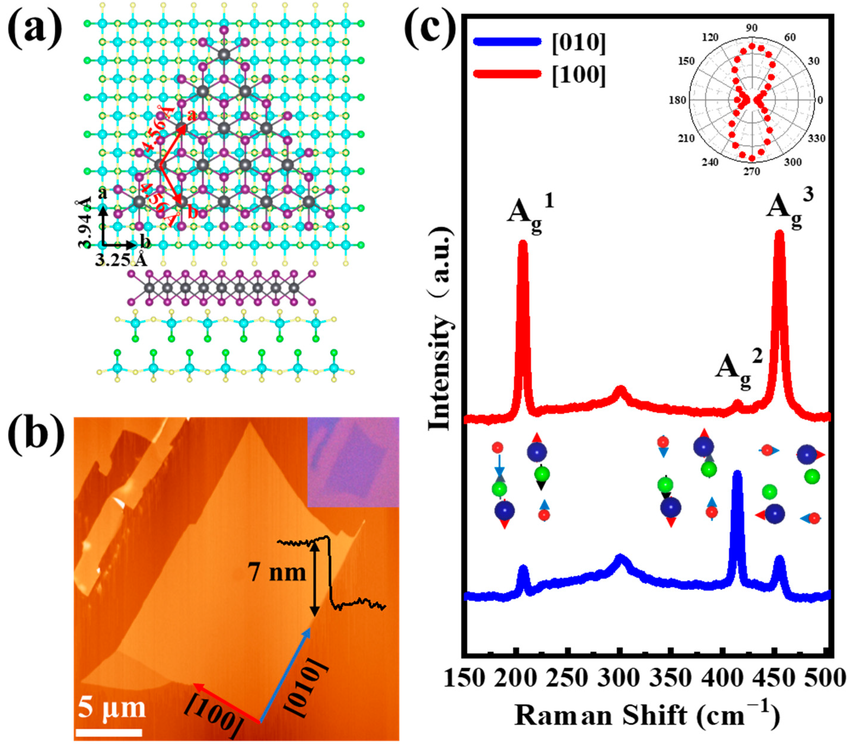
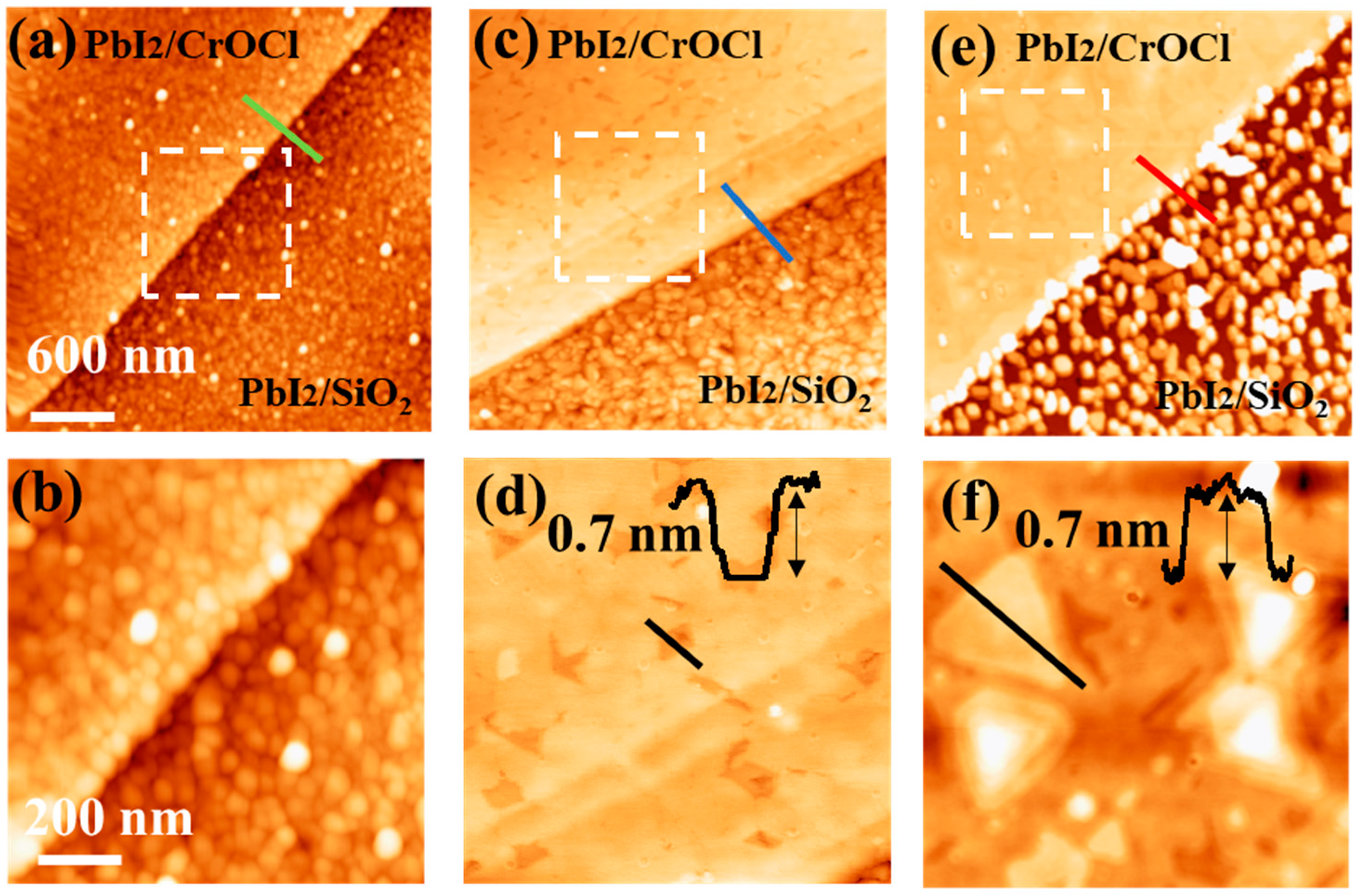
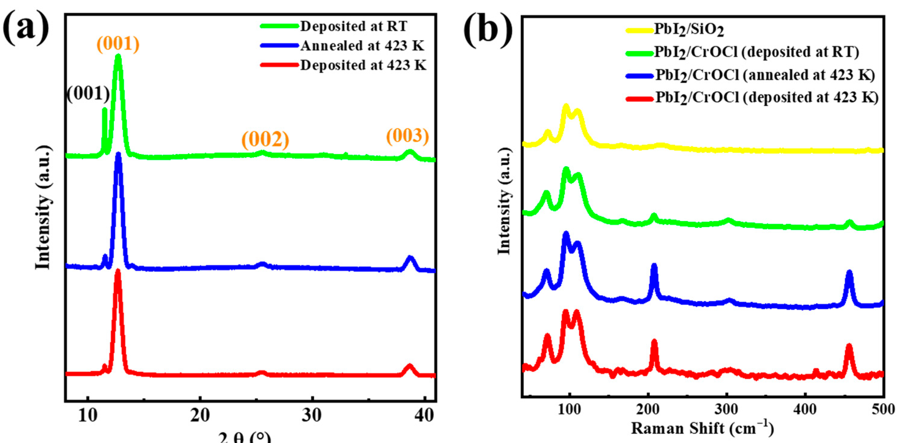
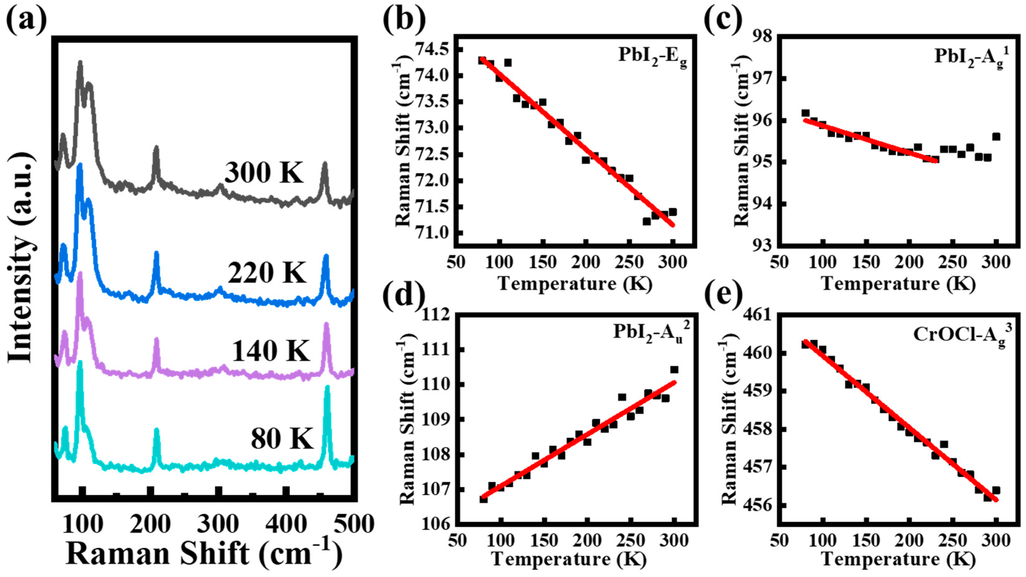
3. Results and Discussion

Owing to the small exfoliation energy of CrOCl of 0.2 J/m2 [23], thin−layered nanoflakes can be easily exfoliated from bulk crystals. Figure 1b shows a representative AFM image of the exfoliated thin−layered CrOCl nanoflake, and the corresponding thickness was ~7 nm. The obvious layered fracture of exfoliated nanoflake confirmed the low vdW force between the layers [18]. The roughness of the CrOCl nanoflake surface was 0.41 nm, representing the positive air stability [29] and the cleanliness, which were helpful for the interface coupling in PbI2/CrOCl heterostructures. The corresponding OM image is shown at the top right corner in Figure 1b. The fracture directions of the CrOCl nanoflake represent two mutually perpendicular ones because the ideal tensile strength was higher [30].
To identify the accurate crystalline directions of CrOCl nanoflakes, Raman scattering measurements were performed. Figure 1c shows two typical Raman spectra of CrOCl nanoflake with the polarization of incident laser along the long straight edge (blue) and the short straight edge (red) at room temperature. There are three peaks located at 207, 414, and 455 cm−1 ascribed to the A g 1 , A g 2 , and A g 3 modes of CrOCl, respectively, in agreement with previous works [17]. The corresponding atomic vibrations of these three optical phonon modes were inserted. The A g 1 and A g 2 modes belong to the out−of−plane vibration model along the [001] direction, while the A g 3 mode belongs to the in−plane mode along the [100] direction [17]. The relative intensity of these modes is totally different along the two given directions. The difference in maximum intensity direction between the A g 1 and A g 2 modes might be caused by the electronic states involved in Raman scattering affected by phonon energy [31]. The additional peak located at 300 cm−1 arose from the strain inside the SiO2/Si substrate [32]. It is reported that the crystalline orientations of low symmetry 2D materials, such as ReS2, b−As, and MoO3, can be determined by angle−resolved polarization Raman measurements [33,34,35]. The orientation of the A g 1 mode could be decomposed to the components along the [001] and [100] directions, respectively [17,36]. The maximum intensity of the A g 1 mode existed while the incident light was parallel to the [100] direction in polarized Raman spectra. The inserted intensity polar plot of the A g 1 mode in Figure 1c shows a period of 180° and maximum intensity along the short straight edge, indicating that the long straight edge was along the [010] direction while the short one was along the [100] direction. The Raman intensity mapping image of the A g 1 mode in Figure S1 (Supplementary Materials) presents a uniform contrast, indicating that the CrOCl nanoflake possessed a high crystalline degree. These results guarantee that the high quality of the exfoliated CrOCl nanoflakes is suitable for our further investigations.
The structural properties of vertical PbI2/CrOCl heterostructures were characterized using AFM. Firstly, PbI2 was deposited onto the substrate maintained at room temperature. Different from our previous reports on MoS2 and MoSe2 [21,22], PbI2 aggregated into semispherical granules but not 2D flat films on CrOCl nanoflakes, as shown in the typical AFM image in Figure 2a. The bright protrusions over the whole substrate surface indicate that PbI2 had similar growth behaviors on CrOCl as those on SiO2 at room temperature. It is clearer in the zoomed−in AFM image from the white−dashed box area in Figure 2b. The statistical grain sizes of PbI2 clusters on CrOCl and SiO2 substrates were almost the same as shown in green and red bars, respectively, in Figure 2g. The same is true for the nucleation densities. The corresponding surface roughness was 1.25 and 1.55 nm, respectively. This might be related to the large diffusion barrier that induced limited diffusion lengths of PbI2 on both surfaces. Post−annealing would possibly improve the quality of the PbI2 films. The as−deposited samples were sequentially annealed up to ~473 K in steps of ~50 K for 1 h at each step. It was found that annealing at ~423 K caused the PbI2 on CrOCl to recrystallize into a 2D form with an atomically flat top surface, as shown in Figure 2c,d, while those on SiO2 were still in granule form but larger, as shown by the yellow bars in Figure 2g. Post−annealing at ~473 K led to PbI2 desorption, while post−annealing at ~373 K had a less obvious effect on the films, as shown in Figure S2. The corresponding surface roughness for annealing at ~423 K was reduced to 0.53 and 0.96 nm on CrOCl and SiO2, respectively. The still rough surface of PbI2 on CrOCl was ascribed to the single−layer deep (0.70 nm) pits, as shown in the profile along the black line in Figure 2d. The statistical graph in Figure S3 shows that the number of pits in the post−annealed sample was significantly less than that in the as−deposited sample. The above results confirm that the growth of PbI2 on CrOCl is diffusion−limited at room temperature.
To realize the vdW epitaxy of PbI2 on CrOCl, the substrate temperature was kept at 423 K during the deposition. As shown in the AFM image in Figure 2e,f, 2D films with a surface roughness of 0.74 nm with some triangular features on top were prepared on CrOCl, while the larger and isolated PbI2 islands were prepared on SiO2, as shown in the blue bars in Figure 2g. The corresponding line profile shows that the triangular features had thicknesses of 0.70 nm, the same as that of the single−layer PbI2. Some of them have thicknesses of multiples of 0.70 nm, meaning multilayers. The size of PbI2 islands is much larger than those in the previous two cases, as shown in Figure 2g. Interestingly, the triangular features show an obvious orientation preference. Figure S4 shows the statistical diagram of the orientation of PbI2 on CrOCl in triangular islands. We define the included angle between one side of the triangular island and the [010] direction of CrOCl as the twist angle. The statistical diagram shows 180° intervals, which is similar to the case of the highly oriented PbI2 on mica observed by Debjit Ghoshal et al. [37], indicating the existence of vdW epitaxy here. Such uniform orientation of PbI2 nanoflakes ensures they merge into a single−crystalline flake on CrOCl during the growth process. According to the crystal structure of triangular and hexagonal single−crystal PbI2 nanoflakes fabricated using the PVD method [38,39], the sides of the PbI2 triangular nanoflakes on CrOCl could be determined to be [ 1 ¯ 100]. Thus, the epitaxial relationship between PbI2 and CrOCl could be determined to be that the [ 1 ¯ 100] direction of PbI2 was parallel to the [010] direction of the CrOCl nanoflake. The lattice spacing values of PbI2 in [ 1 ¯ 100] and [ 1 ¯ 1 ¯ 20] were 4.56 and 3.95 nm, respectively, and those for CrOCl in [010] and [100] were 3.25 and 3.94 nm, respectively. The atomic model built according to the above results in Figure 1a shows that the lattice mismatch was 0.21% and 0.25% along the CrOCl [010] and [100] directions, respectively, which were small enough, justifying our proposed atomic model.
As the substrate temperature increases, the molecules gain thermal energy to merge into larger particles [40]. The statistical results in Figure 2g show that the average grain sizes of the as−deposited PbI2 on CrOCl and SiO2 were 41.16 and 50.58 nm, respectively. Upon annealing at 423 K, the average grain size of PbI2 on SiO2 increased to 70.65 nm, while that deposited at 423 K enlarged to 130.54 nm. This can be further demonstrated in the line profiles across the CrOCl edges for the three cases, as shown in Figure 2h. For the first two cases, the line profiles look smooth because the PbI2 films on both sides were compact. For the last case, the line profile shows ~22 nm bumps because PbI2 nucleated into larger clusters with an exposed SiO2 surface. According to the good epitaxial relationship between PbI2 and CrOCl, we speculate that there were no interfaces or stacking layers which might trap or aggregate defect trapping during the fabrication process.
Figure 3a shows the XRD patterns taken from the three kinds of samples. The positions of diffraction peaks are basically the same. The peak located at 11.5° belongs to the (001) plane of the CrOCl nanoflake [17]. The high intensity of this peak in the samples of PbI2 films deposited at room temperature was caused by the high coverage of exfoliated CrOCl nanoflake. The other characteristic peaks located at 12.6°, 25.4°, and 38.7° belong to the (001), (002), and (003) crystal planes of 2H−phase PbI2, respectively, in agreement with previous studies [11]. Different from our previous reports [22], all three peaks appear much broader, maybe ascribed to the smaller thickness of the deposited PbI2. According to the well−known Debye−Scherrer formula [41],
D = 0.94   λ β   c o s   θ     ,
where D is the grain size, λ is the wavelength of the scattered radiation, β is the width−width at half maxima of the diffraction peak, and θ is the scattering angle, the average PbI2 thickness in the three cases are calculated to be 10 ± 2 nm.
Figure 3b shows the typical normalized Raman spectra of PbI2/CrOCl heterostructure in the above three cases, as well as that of pure PbI2 on SiO2/Si substrate (solid green curve). The peaks were observed at 70, 95, and 110 cm−1, corresponding to the E g (in−plane), A g 1 (out−of−plane), and A u 2 (longitudinal acoustic mode) modes of PbI2, respectively [42,43]. Different from the E g and A g 1 modes belonging to optical phonon modes, the A u 2 mode is a kind of non−Raman−active acoustic mode with vibration along the [001] direction, which is hard to observe most times [44]. However, because the deposited PbI2 films have the interlayer restoring force, which results in the nonzero frequencies, the A u 2 mode could be observed at the backscattering Raman configuration [44,45]. Because the out−of−plane phonon intensity decreased faster than the in−plane phonon intensity as the thickness increased, the ratio of Raman intensity (I ( A g 1 )/I ( E g )) could be used to quickly determine the thicknesses of the PbI2 films [46]. The ratios for the three cases were 1.83, 2.10, and 1.54, respectively, consistent with the above discussions. The fitted phonon mode positions and widths of the three samples are summarized in Table 1. It can be seen that the mode positions in all the PbI2 samples were basically the same, but the mode peak widths for the last case were obviously smaller than the others, confirming the improved crystal quality. Therefore, the peak intensity of A u 2 mode increased in the last case.
TDRS measurements were performed on the PbI2/CrOCl vdW heterostructure with the highest quality to demonstrate the possible substrate effect. Four selected spectra are shown in Figure 4a. The peak positions of PbI2 are basically unchanged through the whole temperature range, especially for the A g 1 mode. However, the A u 2 mode displays an obvious enhancement in intensity as the temperature increases. The measured peak positions of the E g , A g 1 , and A u 2 modes as functions of temperature are plotted in Figure 4b–d, respectively. The E g mode exhibits linear redshift, while the A u 2 mode shows linear blueshift as the temperature increases. The abnormal blueshift of the A g 1 mode at temperatures above 260 K could have come from the slip between PbI2 and CrOCl substrate induced by thermal expansion mismatch, similar to previous reports [43,47]. The E g mode moved from 74.3 to 71.4 cm−1, while the A g 1 mode moved from 96.2 to 95.6 cm−1 over the whole temperature range, indicating the temperature dependence of the E g mode was stronger than that of the A g 1 mode. The temperature dependence of the Raman mode position could be fitted by the Gr u ¨ neisen model [48]:
ω = ω0 + χT
where ω0 is the peak position extended to 0 K and χ is the first−order temperature coefficient. The first−order temperature coefficients are calculated to be χ E g   PbI 2 / CrOCl = −(1.44 ± 0.05) × 10−2 cm−1 K−1, χ A g 1   PbI 2 / CrOCl = −(6.48 ± 0.05) × 10−3 cm−1 K−1 (only extracting the measured data at a temperature range below 240 K) and χ A u 2   PbI 2 / CrOCl = (1.48 ± 0.06) × 10−2 cm−1 K−1, respectively. For comparison to a previous study of PbI2/SiO2/Si [43] ( χ E g   PbI 2 = −1.80 × 10⁻² cm−1 K−1, χ A g 1   PbI 2 = −0.60 × 10⁻² cm−1 K−1  χ A u 2   PbI 2 = −0.10 × 10⁻² cm−1 K−1), the first−order coefficients of the A g 1 and A u 2 modes in PbI2/CrOCl heterostructure obviously increased. The interfering factor of the temperature dependence of the Raman peak position could be attributed to anharmonic phonon–phonon coupling, thermal expansion, and the substrate effect [49,50,51]. The increase of the first−order coefficient in the A g 1 mode and the abnormal blueshift of the A u 2 mode position could have originated from the increase in the number of up−conversion channels in the anharmonic phonon–phonon coupling, which could be induced by the CrOCl substrate, but more research is needed to prove this [52,53]. The peak widths of the E g , A g 1 , and A u 2 modes broadened as the temperature increased, originating from the anharmonic phonon–phonon coupling [54,55], as shown in Figure S5. In addition, Figure 4e shows the temperature dependence of the A g 3 mode of the CrOCl substrate. In agreement with previous studies [17,23], the A g 3 mode exhibits redshift as the temperature increases, and the fitted first−order temperature coefficient is χ A g 3   CrOCl = −(1.89 ± 0.04) × 10−2 cm−1 K−1.

4. Conclusions

In summary, the investigation of multilayered PbI2/CrOCl vdW heterostructures was reported in this paper. The morphology of PbI2 films on CrOCl nanoflakes changed from granules to oriented 2D nanoflakes with flat and smooth top surfaces while being fabricated at an elevated substrate temperature of 423 K. In addition, both the A g 1 and A u 2 modes in PbI2 showed anomalous blueshift as the temperature increased in the PbI2/CrOCl heterostructure in the temperature−dependent Raman spectra.

Supplementary Materials

The following supporting information can be downloaded at: https://www.mdpi.com/article/10.3390/cryst13010104/s1, Figure S1: Raman intensity mapping image of Ag1 mode of exfoliated CrOCl nanoflake, Figure S2: AFM images of PbI2 films annealed at 373 K (a) and 473 K (c) after deposited at room temperature. (b,d) The corresponding high−resolution images from the white square area inside the figure (a,c), respectively, Figure S3: AFM image of PbI2/CrOCl heterostructure which deposited at room temperature (a) and annealed after deposited (b), the number of grain and defects are highlighted inside either, Figure S4: (a) AFM image of PbI2/CrOCl heterostructure deposited at 423 K, the triangular islands show the same orientation. (b) Statistical diagram of the orientation of PbI2 triangular islands. (c) Phase image of PbI2/CrOCl heterostructure showing triangular islands, the [−1100] direction of PbI2 mostly along the [010] direction of CrOCl nanoflake, Figure S5: FWMH of E g (a), A g 1 (b) and A u 2 (c) modes at temperature dependent Raman spectra. Each FWMH is linearly broadened as the temperature increasing.

Author Contributions

Experimental design, S.Y.; methodology, H.H.; data curation, S.Y., J.J. and D.Y.; data analysis, S.Y. and X.G.; writing—original draft, S.Y., X.G. and H.H.; writing—review and editing, S.Y., X.G. and H.H.; supervision, H.X., M.L., and F.O.; funding acquisition, H.H. and Y.G. All authors have read and agreed to the published version of the manuscript.

Funding

This research was funded by the National Natural Science Foundation (NSF) of China (Grants No. 11874427), the National Key Research and Development Program of China (Grant No. 2017YFA0206602), the Fundamental Research Funds for the Central Universities for Central South University (Grant No. 2021zzts0506), and the National Science Foundation (Grant No. DMR 1903962).

Data Availability Statement

Not applicable.

Conflicts of Interest

There are no conflicts of interest to declare.

References

  1. Kim, Y.; Cruz, S.S.; Lee, K.; Alawode, B.O.; Choi, C.; Song, Y.; Johnson, J.M.; Heidelberger, C.; Kong, W.; Choi, S.; et al. Remote Epitaxy through Graphene Enables Two−Dimensional Material−Based Layer Transfer. Nature 2017, 544, 340–343. [Google Scholar] [CrossRef] [PubMed]
  2. Britnell, L.; Ribeiro, R.M.; Eckmann, A.; Jalil, R.; Belle, B.D.; Mishchenko, A.; Kim, Y.J.; Gorbachev, R.V.; Georgiou, T.; Morozov, S.V.; et al. Strong Light−Matter Interactions in Heterostructures of Atomically Thin Films. Science 2013, 340, 1311–1314. [Google Scholar] [CrossRef] [Green Version]
  3. Geim, A.K.; Grigorieva, I.V. Van Der Waals Heterostructures. Nature 2013, 499, 419–425. [Google Scholar] [CrossRef] [Green Version]
  4. Gong, Y.; Lin, J.; Wang, X.; Shi, G.; Lei, S.; Lin, Z.; Zou, X.; Ye, G.; Vajtai, R.; Yakobson, B.I.; et al. Vertical and In−Plane Heterostructures from WS2 /MoS2 Monolayers. Nat. Mater. 2014, 13, 1135–1142. [Google Scholar] [CrossRef] [Green Version]
  5. Zhang, J.; Huang, Y.; Tan, Z.; Li, T.; Zhang, Y.; Jia, K.; Lin, L.; Sun, L.; Chen, X.; Li, Z.; et al. Low−Temperature Heteroepitaxy of 2D PbI2/Graphene for Large−Area Flexible Photodetectors. Adv. Mater. 2018, 30, 1803194. [Google Scholar] [CrossRef] [PubMed]
  6. Yang, W.; Chen, G.; Shi, Z.; Liu, C.C.; Zhang, L.; Xie, G.; Cheng, M.; Wang, D.; Yang, R.; Shi, D.; et al. Epitaxial Growth of Single−Domain Graphene on Hexagonal Boron Nitride. Nat. Mater. 2013, 12, 792–797. [Google Scholar] [CrossRef]
  7. Zhu, L.; Yang, T.; Zhong, Y.; Jin, Z.; Zhang, X.; Hu, C.; Wang, Z.; Wu, Z.; Zhang, Z.; Shi, Z.; et al. Scalable and Versatile Transfer of Sensitive Two−Dimensional Materials. Nano Lett. 2022, 22, 2342–2349. [Google Scholar] [CrossRef]
  8. Yan, R.; Fathipour, S.; Han, Y.; Song, B.; Xiao, S.; Li, M.; Ma, N.; Protasenko, V.; Muller, D.A.; Jena, D.; et al. Esaki Diodes in van Der Waals Heterojunctions with Broken−Gap Energy Band Alignment. Nano Lett. 2015, 15, 5791–5798. [Google Scholar] [CrossRef] [Green Version]
  9. Zhang, L.; Sharma, A.; Zhu, Y.; Zhang, Y.; Wang, B.; Dong, M.; Nguyen, H.T.; Wang, Z.; Wen, B.; Cao, Y.; et al. Efficient and Layer−Dependent Exciton Pumping across Atomically Thin Organic–Inorganic Type−I Heterostructures. Adv. Mater. 2018, 30, 1803986. [Google Scholar] [CrossRef] [PubMed]
  10. Baranowski, M.; Surrente, A.; Klopotowski, L.; Urban, J.M.; Zhang, N.; Maude, D.K.; Wiwatowski, K.; Mackowski, S.; Kung, Y.C.; Dumcenco, D.; et al. Probing the Interlayer Exciton Physics in a MoS2/MoSe2/MoS2 van Der Waals Heterostructure. Nano Lett. 2017, 17, 6360–6365. [Google Scholar] [CrossRef]
  11. Wang, Y.; Gan, L.; Chen, J.; Yang, R.; Zhai, T. Achieving Highly Uniform Two−Dimensional PbI2 Flakes for Photodetectors via Space Confined Physical Vapor Deposition. Sci. Bull. 2017, 62, 1654–1662. [Google Scholar] [CrossRef] [Green Version]
  12. Zhong, M.; Zhang, S.; Huang, L.; You, J.; Wei, Z.; Liu, X.; Li, J. Large−Scale 2D PbI2 Monolayers: Experimental Realization and Their Indirect Band−Gap Related Properties. Nanoscale 2017, 9, 3736–3741. [Google Scholar] [CrossRef] [PubMed]
  13. Toulouse, A.S.; Isaacoff, B.P.; Shi, G.; Matuchová, M.; Kioupakis, E.; Merlin, R. Frenkel−like Wannier−Mott Excitons in Few−Layer PbI2. Phys. Rev. B 2015, 91, 165308. [Google Scholar] [CrossRef] [Green Version]
  14. Sun, L.; Wang, C.; Xu, L.; Wang, J.; Liu, X.; Chen, X.; Yi, G.C. SbSI Whisker/PbI2 Flake Mixed−Dimensional van Der Waals Heterostructure for Photodetection. Cryst. Eng. Comm. 2019, 21, 3779–3787. [Google Scholar] [CrossRef]
  15. Ri, C.H.; Han, H.U.; Kim, Y.S.; Jong, U.G.; Kye, Y.H.; Yu, C.J. Enhancing the Photocatalytic Hydrogen Evolution Performance of the CsPbI3/MoS2 Heterostructure with Interfacial Defect Engineering. J. Phys. Chem. Lett. 2022, 13, 4007–4014. [Google Scholar] [CrossRef]
  16. Wang, R.; Cui, Q.; Zhu, W.; Niu, Y.; Liu, Z.; Zhang, L.; Wu, X.; Chen, S.; Song, L. In−Plane Optical Anisotropy of Two−Dimensional VOCl Single Crystal with Weak Interlayer Interaction. Chin. Phys. B 2022, 31, 096802. [Google Scholar] [CrossRef]
  17. Zhang, T.; Wang, Y.; Li, H.; Zhong, F.; Shi, J.; Wu, M.; Sun, Z.; Shen, W.; Wei, B.; Hu, W.; et al. Magnetism and Optical Anisotropy in van Der Waals Antiferromagnetic Insulator CrOCl. ACS Nano 2019, 13, 11353–11362. [Google Scholar] [CrossRef]
  18. Wang, M.; Zhang, J.; Wang, Z.; Wang, C.; van Smaalen, S.; Xiao, H.; Chen, X.; Du, C.; Xu, X.; Tao, X. Broadband CrOCl Saturable Absorber with a Spectral Region Extension to 10.6 µm. Adv. Optical Mater. 2019, 8, 1901446. [Google Scholar] [CrossRef]
  19. Sun, R.J.; Liu, R.; Lu, J.J.; Zhao, X.W.; Hu, G.C.; Yuan, X.B.; Ren, J.F. Reversible Switching of Anomalous Valley Hall Effect in Ferrovalley Janus 1T−CrOX (X = F, Cl, Br, I) and the Multiferroic Heterostructure CrOX/In2Se3. Phys. Rev. B 2022, 105, 235416. [Google Scholar] [CrossRef]
  20. Liu, W.; Guo, X.; Schwartz, J.; Xie, H.; Dhale, N.U.; Sung, S.H.; Kondusamy, A.L.N.; Wang, X.; Zhao, H.; Berman, D.; et al. A Three−Stage Magnetic Phase Transition Revealed in Ultrahigh−Quality van Der Waals Bulk Magnet CrSBr. ACS Nano 2022, 16, 15917–15926. [Google Scholar] [CrossRef]
  21. Xiao, J.; Zhang, L.; Zhou, H.; Shao, Z.; Liu, J.; Zhao, Y.; Li, Y.; Liu, X.; Xie, H.; Gao, Y.; et al. Type−II Interface Band Alignment in the VdW PbI2−MoSe2 Heterostructure. ACS Appl. Mater. Interfaces 2020, 12, 32099–32105. [Google Scholar] [CrossRef]
  22. Xiao, J.; Liu, J.; Sun, K.; Zhao, Y.; Shao, Z.; Liu, X.; Yuan, Y.; Li, Y.; Xie, H.; Song, F.; et al. PbI2−MoS2 Heterojunction: Van Der Waals Epitaxial Growth and Energy Band Alignment. J. Phys. Chem. Lett. 2019, 10, 4203–4208. [Google Scholar] [CrossRef]
  23. Zheng, X.; Wei, Y.; Wei, Z.; Luo, W.; Guo, X.; Zhang, X.; Liu, J.; Chen, Y.; Peng, G.; Cai, W.; et al. Highly Anisotropic Thermal Conductivity of Few−Layer CrOCl for Efficient Heat Dissipation in Graphene Device. Nano Res. 2022, 15, 9377–9385. [Google Scholar] [CrossRef]
  24. Zheng, X.; Wei, Y.; Zhang, X.; Wei, Z.; Luo, W.; Guo, X.; Liu, J.; Peng, G.; Cai, W.; Huang, H.; et al. Symmetry Engineering Induced In−Plane Polarization in MoS2 through Van Der Waals Interlayer Coupling. Adv. Funct. Mater. 2022, 32, 2202658. [Google Scholar] [CrossRef]
  25. You, S.; Shao, Z.; Guo, X.; Jiang, J.; Liu, J.; Wang, K.; Li, M.; Ouyang, F.; Deng, C.; Song, F.; et al. Growth Behaviors and Emission Properties of Co−Deposited MAPbI3 Ultrathin Films on MoS2. Chin. Phys. B 2022, 32, 017901. [Google Scholar] [CrossRef]
  26. Shao, Z.; You, S.; Guo, X.; Xiao, J.; Liu, J.; Song, F.; Xie, H.; Sun, J.; Huang, H. Temperature−Dependent Photoluminescence of Co−Evaporated MAPbI3 Ultrathin Films. Results Phys. 2022, 34, 105326. [Google Scholar] [CrossRef]
  27. Shao, Z.; Xiao, J.; Guo, X.; You, S.; Zhang, Y.; Li, M.; Song, F.; Zhou, C.; Xie, H.; Gao, Y.; et al. Emission Properties of Sequentially Deposited Ultrathin CH3NH3PbI3/MoS2 Heterostructures. Curr. Appl. Phys. 2022, 36, 27–33. [Google Scholar] [CrossRef]
  28. AL−Makeen, M.M.; Guo, X.; Wang, Y.; Yang, D.; You, S.; Yassine, M.; Jiang, J.; Song, P.B.; Shi, Y.G.; Xie, H.; et al. Investigation of the Electron–Phonon Coupling in Dirac Semimetal PdTe2 via Temperature−Dependent Raman Spectroscopy. Phys. Status Solidi RRL 2022, 16, 2200257. [Google Scholar] [CrossRef]
  29. Zhang, T.; Zhang, Y.; Huang, M.; Li, B.; Sun, Y.; Qu, Z.; Duan, X.; Jiang, C.; Yang, S. Tuning the Exchange Bias Effect in 2D van Der Waals Ferro−/Antiferromagnetic Fe3GeTe2/CrOCl Heterostructures. Adv. Sci. 2022, 9, 2105483. [Google Scholar] [CrossRef] [PubMed]
  30. Gao, E.; Lin, S.Z.; Qin, Z.; Buehler, M.J.; Feng, X.Q.; Xu, Z. Mechanical Exfoliation of Two−Dimensional Materials. J. Mech. Phys. Solids 2018, 115, 248–262. [Google Scholar] [CrossRef]
  31. Huang, S.; Tatsumi, Y.; Ling, X.; Guo, H.; Wang, Z.; Watson, G.; Puretzky, A.A.; Geohegan, D.B.; Kong, J.; Li, J.; et al. In−Plane Optical Anisotropy of Layered Gallium Telluride. ACS Nano 2016, 10, 8964–8972. [Google Scholar] [CrossRef]
  32. Shi, J.; Wu, D.; Zheng, X.; Xie, D.; Song, F.; Zhang, X.; Jiang, J.; Yuan, X.; Gao, Y.; Huang, H. From MoO2@MoS2 Core–Shell Nanorods to MoS2 Nanobelts. Phys. Status Solidi B 2018, 255, 1800254. [Google Scholar] [CrossRef]
  33. Wang, Y.; Guo, X.; You, S.; Jiang, J.; Wang, Z.; Ouyang, F.; Huang, H. Giant Quartic−Phonon Decay in PVD−Grown α−MoO3 Flakes. Nano Res. 2022. [Google Scholar] [CrossRef]
  34. Yu, J.; Wang, Y.; Jiang, J.; Liang, Y.; Liu, Y.; Zhong, B.; Quan, S.; Zhou, M.; Ni, Z.; Guo, S. Tunable Anisotropy in ReS2 flakes Achieved by Ar+ ion Bombardment Probed by Polarized Raman Spectroscopy. Appl. Phys. Lett. 2021, 119, 053104. [Google Scholar] [CrossRef]
  35. Wang, Z.; Wang, Y.; Guo, X.; You, S.; Niu, T.; Zhong, M.; Xia, Q.; Huang, H. Phonon Anharmonicity in Exfoliated Black Arsenic Flakes. Appl. Phys. Lett. 2022, 121, 122106. [Google Scholar] [CrossRef]
  36. Xu, C.; Zhang, J.; Guo, Z.; Zhang, S.; Yuan, X.; Wang, L. A First−Principles Study on the Electronic Property and Magnetic Anisotropy of Ferromagnetic CrOF and CrOCl Monolayers. J. Phys. Condens. Matter 2021, 33, 195804. [Google Scholar] [CrossRef] [PubMed]
  37. Ghoshal, D.; Shang, H.; Sun, X.; Wen, X.; Chen, D.; Wang, T.; Lu, Z.; Gupta, T.; Efstathiadis, H.; West, D.; et al. Orientation−Controlled Large−Area Epitaxial PbI2 Thin Films with Tunable Optical Properties. ACS Appl. Mater. Interfaces 2021, 13, 32450–32460. [Google Scholar] [CrossRef]
  38. Guo, Q.; Ye, X.; Zhang, L.; Lin, Q.; Li, C.; Han, Q.; Zheng, X.; Jiang, J.; Zhang, H.; Liu, Y.; et al. Microspacing In−Air Sublimation Growth of Thickness−Controllable Lead Halide Crystal and the Morphology Evolution in Conversion to Perovskite. ACS Appl. Energy Mater. 2022, 5, 1618–1626. [Google Scholar] [CrossRef]
  39. Zhong, M.; Huang, L.; Deng, H.X.; Wang, X.; Li, B.; Wei, Z.; Li, J. Flexible Photodetectors Based on Phase Dependent PbI2 Single Crystals. J. Mater. Chem. C Mater. 2016, 4, 6492–6499. [Google Scholar] [CrossRef]
  40. Devika, M.; Reddy, N.K.; Ramesh, K.; Ganesan, V.; Gopal, E.S.R.; Reddy, K.T.R. Influence of Substrate Temperature on Surface Structure and Electrical Resistivity of the Evaporated Tin Sulphide Films. Appl. Surf. Sci. 2006, 253, 1673–1676. [Google Scholar] [CrossRef]
  41. Cullity, B.D. Elements of X−ray Diffraction; Addison−Wesley Publishing: Boston, MA, USA, 1956. [Google Scholar]
  42. Zhang, Z.; Zheng, W.; Wang, W.; Zhong, D.; Huang, F. Anisotropic Temperature−Dependence of Optical Phonons in Layered PbI2. J. Raman Spectrosc. 2018, 49, 775–779. [Google Scholar] [CrossRef]
  43. Ding, J.; Cheng, P.; Ye, T.; Xu, W.; Zeng, H.; Yao, D.; Pan, X.; Zhang, J. Pressure−Induced Two−Dimensional to Three−Dimensional Structural Phase Transition in 2H−Type Layered Lead Iodide PbI2. Appl. Phys. Lett. 2022, 120, 052106. [Google Scholar] [CrossRef]
  44. Yagmurcukardes, M.; Peeters, F.M.; Sahin, H. Electronic and Vibrational Properties of PbI2: From Bulk to Monolayer. Phys. Rev. B 2018, 98, 085431. [Google Scholar] [CrossRef] [Green Version]
  45. Jorio, A.; Mueller, N.S.; Reich, S. Symmetry−Derived Selection Rules for Plasmon−Enhanced Raman Scattering. Phys. Rev. B 2017, 95, 155409. [Google Scholar] [CrossRef] [Green Version]
  46. Du, L.; Wang, C.; Xiong, W.; Zhang, S.; Xia, C.; Wei, Z.; Li, J.; Tongay, S.; Yang, F.; Zhang, X.; et al. Perseverance of Direct Bandgap in Multilayer 2D PbI2 under an Experimental Strain up to 7.69%. 2D Mater. 2019, 6, 025014. [Google Scholar] [CrossRef]
  47. Yoon, D.; Son, Y.W.; Cheong, H. Negative Thermal Expansion Coefficient of Graphene Measured by Raman Spectroscopy. Nano Lett. 2011, 11, 3227–3231. [Google Scholar] [CrossRef] [PubMed] [Green Version]
  48. Zouboulis, E.S.; Grimsditch, M. Raman Scattering in Diamond up to 1900 K. Phys. Rev. B 1990, 43, 12490. [Google Scholar] [CrossRef] [PubMed]
  49. Guo, X.; Tian, Q.; Wang, Y.; Liu, J.; Jia, G.; Dou, W.; Song, F.; Zhang, L.; Qin, Z.; Huang, H. Phonon Anharmonicities in 7−Armchair Graphene Nanoribbons. Carbon 2022, 190, 312–318. [Google Scholar] [CrossRef]
  50. Umakoshi, T.; Taniguchi, M.; Verma, P. Anharmonic Effects in Single−Walled Carbon Nanotubes Analyzed through Low−Temperature Raman Imaging. J. Phy. Chem. C 2020, 124, 6922–6928. [Google Scholar] [CrossRef]
  51. Tan, S.J.R.; Sarkar, S.; Zhao, X.; Luo, X.; Luo, Y.Z.; Poh, S.M.; Abdelwahab, I.; Zhou, W.; Venkatesan, T.; Chen, W.; et al. Temperature− and Phase−Dependent Phonon Renormalization in 1T−MoS2. ACS Nano 2018, 12, 5051–5058. [Google Scholar] [CrossRef]
  52. Tsujimoto, M.; Tanimura, M.; Tachibana, M. Temperature Dependence of the Raman Spectra of Multilayer Graphene Nanoribbons Fabricated by Unzipping Method. Diam. Relat. Mater. 2020, 109, 108047. [Google Scholar] [CrossRef]
  53. Efthimiopoulos, I.; Mayanna, S.; Stavrou, E.; Torode, A.; Wang, Y. Extracting the Anharmonic Properties of the G−Band in Graphene Nanoplatelets. J. Phys. Chem. C 2020, 124, 4835–4842. [Google Scholar] [CrossRef]
  54. Balkanski, M.; Wallis, R.F.; Haro, E. Anharmonic Effects in Light Scattering Due to Optical Phonons in Silicon. Phys. Rev. B 1983, 28, 1928. [Google Scholar] [CrossRef]
  55. de Andres, P.L.; Guinea, F.; Katsnelson, M.I. Bending Modes, Anharmonic Effects, and Thermal Expansion Coefficient in Single−Layer and Multilayer Graphene. Phys. Rev. B 2012, 86, 144103. [Google Scholar] [CrossRef]
Figure 1. Characterization of thin−layered CrOCl nanoflake. (a) Atom structure of PbI2/CrOCl heterostructure; (b) AFM image of layered CrOCl nanoflake with the thickness and crystal orientation highlighted. The corresponding OM image is inserted at the right top corner; (c) Raman spectra of CrOCl nanoflake along the [010] direction and [100] direction, respectively. There is a strong in−plane anisotropy of the A g mode intensity. The atomic vibrations of A g 1 , A g 2 , and A g 3 modes, and the polar plot of A g 1 mode is inserted.
Crystals 13 00104 g001
Figure 2. Surface morphology evolution of PbI2/CrOCl heterostructures fabricated with different conditions. (a) AFM image of PbI2 films deposited at room temperature; (b) zoomed−in AFM image of PbI2/CrOCl from the white box area in figure; (a,c) AFM images of PbI2 films annealed at 423 K after deposition; (d) zoomed−in AFM image of PbI2/CrOCl from the white box area in figure (c,e) AFM image of PbI2 films deposited at 423 K; (f) zoomed−in AFM image of PbI2/CrOCl from the white box area in figure; (e,g) distribution of PbI2 granule size for three samples; (h) corresponding line profiles across the CrOCl edges in the three samples. The histograms and profiles with green, blue, and red indicate the samples deposited at room temperature, annealed after deposition, and deposited at 423 K, respectively.
Crystals 13 00104 g002aCrystals 13 00104 g002b
Figure 3. XRD patterns (a) and typical Raman spectra (b) of PbI2/CrOCl heterostructure in three cases.
Crystals 13 00104 g003
Figure 4. Temperature−dependent Raman spectra of PbI2/CrOCl heterostructure. (a) Selected and normalized Raman spectra of PbI2/CrOCl heterostructure at selected temperatures. Temperature dependence of peak position of E g (b), A g 1 (c) and A u 2 (d) modes in PbI2. (e) Temperature dependence of peak position of A g 3 mode in CrOCl. The solid red lines represent the linear fitting results.
Crystals 13 00104 g004
Table 1. Phonon mode information of PbI2/CrOCl heterostructure and PbI2.
Phonon ModesPeak Position (cm−1)Peak Width (cm−1)
PbI2/CrOCl
(Deposited at RT)
PbI2/CrOCl
(Annealed at 423 K)
PbI2/CrOCl
(Deposited at 423 K)
PbI2/SiO2PbI2/CrOCl
(Deposited at RT)
PbI2/CrOCl
(Annealed at 423 K)
PbI2/CrOCl
(Deposited at 423 K)
PbI2/SiO2
E g 70.070.571.870.110.79.68.08.3
A g 1 95.495.395.195.19.28.98.08.8
A u 2 110.2109.9109.9109.818.018.715.617.0
Disclaimer/Publisher’s Note: The statements, opinions and data contained in all publications are solely those of the individual author(s) and contributor(s) and not of MDPI and/or the editor(s). MDPI and/or the editor(s) disclaim responsibility for any injury to people or property resulting from any ideas, methods, instructions or products referred to in the content.

