
Annealing Engineering in the Growth of Perovskite Grains
by
 , and
, and
Lan Wang
1,2,3, 
Guilin Liu
1,2,
Xi Xi
1,2,*,
Guofeng Yang
1,2,
Lifa Hu
1,2,3,
Bingjie Zhu
4,
Yifeng He
5,
Yushen Liu
6,7,
Hongqiang Qian
8,
Shude Zhang
8 and
Huachao Zai
9,* 1
School of Science, Jiangnan University, Wuxi 214122, China
2
International Joint Research Center for Photoresponse Functional Molecular Materials, Wuxi 214122, China
3
School of Internet of Things Engineering, Jiangnan University, Wuxi 214122, China
4
Wuxi Institution of Supervision & Testing on Product Quality, Wuxi 214101, China
5
Zhejiang Beyondsun Green Energy Technology Co., Ltd., Huzhou 313200, China
6
Suzhou Key Laboratory of Advanced Lighting and Display Technologies, School of Electronic and Information Engineering, Changshu 215556, China
7
School of Electronic and Information Engineering, Changshu Institute of Technology, Changshu 215556, China
8
Suzhou Talesun Solar Technologies Co., Ltd., Suzhou 215542, China
9
School of Materials Science and Engineering, Peking University, Beijing 100871, China
*
Authors to whom correspondence should be addressed.
Crystals 2022, 12(7), 894; https://doi.org/10.3390/cryst12070894
Submission received: 6 May 2022
/
Revised: 9 June 2022
/
Accepted: 20 June 2022
/
Published: 24 June 2022
(This article belongs to the Special Issue Advances of Perovskite Solar Cells)
Abstract
:Perovskite solar cells (PSCs) are a promising and fast-growing type of photovoltaic cell due to their low cost and high conversion efficiency. The high efficiency of PSCs is closely related to the quality of the photosensitive layer, and the high-quality light absorbing layer depends on the growth condition of the crystals. In the formation of high-quality crystals, annealing is an indispensable and crucial part, which serves to evaporate the solvent and drive the crystallization of the film. Various annealing methods have different effects on the promotion of the film growth process owing to the way they work. Here, this review will present a discussion of the growth puzzles and quality of perovskite crystals under different driving forces, and then explain the relationship between the annealing driving force and crystal growth. We divided the main current annealing methods into physical and chemical annealing, which has never been summarized before. The main annealing methods currently reported for crystal growth are summarized to visualize the impact of annealing design strategies on photovoltaic performance, while the growth mechanisms of thin films under multiple annealing methods are also discussed. Finally, we suggest future perspectives and trends in the industrial fabrication of PSCs in the future. The review promises industrial manufacturing of annealed PSCs. The review is expected to facilitate the industrial fabrication of PSCs.
1. Introduction
Halide perovskite solar cells (PSCs) have become the research focus in the field of photovoltaic cells due to their superior optoelectronic properties, excellent absorption coefficients, high conversion efficiency and tunable optical band gap [1,2,3,4]. In 2009, PSCs achieved an efficiency of 3.8% when the perovskite material was first applied in solar cells [5]. The latest efficiency of perovskite solar cells has exceeded 25% in recent years, after only a few years of development [6]. High-efficiency perovskite cells rely on the preparation of high-quality layers; the general fabrication process involves spin-coating the configured precursor solution onto the substrate and completing the crystal crystallization by annealing the substrate at a specific temperature for a period of time. Annealing is utilized to evaporate the organic polar solvent and drive the crystalline transformation of the perovskite, which can control the morphological and structural properties of films [7,8]. Heating materials up to a particular temperature and maintaining it for the given time is a thermal treatment method which has widely been applied in all types of solar cells. The thermal treatment will eliminate residual stresses, internal defects and adjust the microstructure within the materials [9,10,11,12]. In the fabrication of silicon cells, sintering is carried out by annealing, which ultimately reduces the resistivity and creates the great ohmic contact at the electrodes on the surface of the silicon solar cells [13,14,15,16,17]. In the crystallization of perovskite crystals, the annealing methods, duration, and temperature strongly affect the crystalline quality and crystal structure in perovskite film. Reducing the annealing time and improving crystal quality are the focus of current research in annealing treatments [18,19,20,21]. Hence, many researchers have developed various annealing methods, including thermal annealing, photo-annealing and solvent annealing, among others, to shorten the annealing treatment time or enhance the crystal quality [21,22,23]. However, there is a lack of systematical discussion about the effects of various annealing methods on the perovskite fabrication process, which prevents the further development of the PSCs.
In this paper, we have summarized the various annealing methods which have been employed in the fabrication of PSCs. The three-dimensional lead-based perovskites were the main object of this discussion. Then, we have reviewed the principles of the different annealing methods and then introduced detailed influences of annealing methods on films. Finally, a comparative discussion of the differences between the various annealing methods is provided. In general, we have proposed some future technological trends in the commercial manufacture of PSCs.
2. Conditions and Effects of Annealing
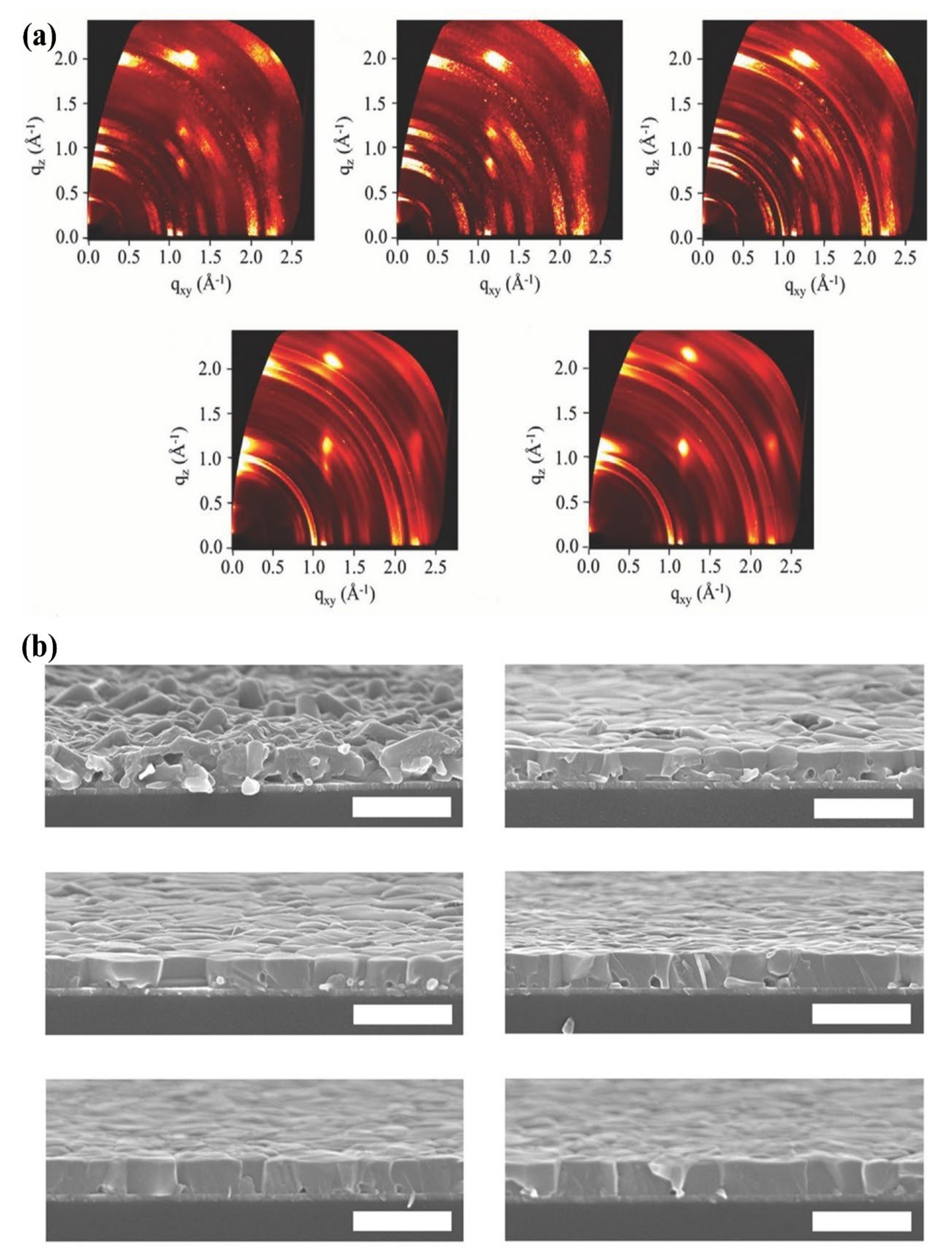
The perovskite films, after spin-coating the precursor solution, are initially maintained in a metastable state, containing complex internal crystalline phases tuned by polar solvent intermediate phases [24,25]. The transformation from wet film to perovskite is driven by an oversaturated environment due to the reduction of solvent [26,27], thus crystallization necessarily requires the removal of organic solvents. In general, researchers have used thermal annealing to evaporate the solvent, which was driven off the film by heat and thus promoted the transformation of the intermediate phase into the pure α phase [28,29]. In situ grazing incidence wide angle X-ray scattering (GIWAXS) results were used to reveal the evolution of CH3NH3PbI3 - xClx perovskite from the intermediate phase to the ABX3 structure in thermal treatment (Figure 1a) [28].
The film contained mostly peaks of the precursor intermediate phase inside at the moment t = 0. As t gradually increased, some intermediate phases disappeared and the perovskite α phase was formed; the diffraction intensity of perovskite was enhanced, and the crystal orientation sharply emerged. The crystallization process in thermal annealing followed the mode of top-down. During the annealing process, the perovskite film in contact with the air first grew into an ordered structure, as displayed in the scanning electron microscopy (SEM) results (Figure 1b); the pinholes during growth existed on the substrate side, which was a sign of incomplete growth of the film [25]. The change in the structure of the perovskite in annealing was also accompanied by an evolution of the optoelectronic properties.
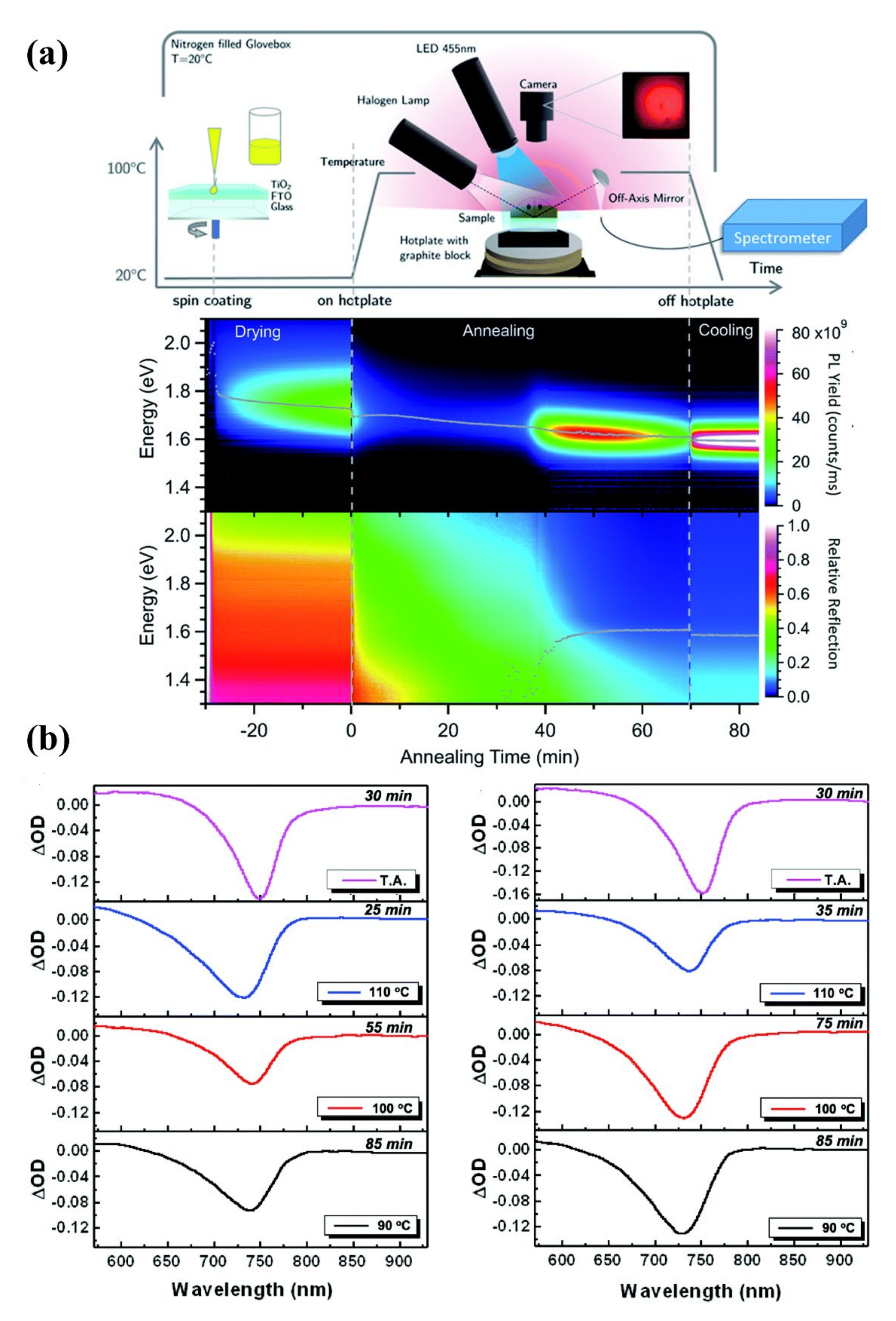
In situ optical reflectometry showed the evolution of the photoelectric properties of the film in crystallization (Figure 2a) [29]. The band gap of the unannealed sample was close to 1.7 eV. The emission intensity of the annealed sample decreased immediately within the first minute, and increased again after a period of annealing, with the band gap decreasing continuously to 1.6 eV. A strong absorption was displayed at 1.6 eV after cooling. The transient light absorption (TAS) curves of the films at different annealing times also exhibited this shift in band gap (Figure 2b) [30]. All samples exhibited the blue shift of the delta optical density (ΔOD) peak compared to typical thermally annealed (TA) samples, which were attributed to the increase in band gap with changing temperature [31]. The researchers attributed this result to the splitting of the bonding and antibonding orbitals of CH3NH3PbI3 during annealing. The thermal extension of the lattice affected the conduction band minimum and valence band maximum, causing an overall band gap increase. The family of perovskite materials used in PSCs usually has the chemical formula of ABX3 with a corner-sharing BX6 octahedral and AX12 cuboctahedra [32], where the A-site is usually occupied by an organic or inorganic monovalent cation (methylammonium: MA, formamidinium: FA, Cs), the B-site is divalent lead cation (Pb, Sn), and the X-site is a halogen [33,34,35,36]. Annealing is the rearrangement of ions inside the perovskite film. The lead counter ions have obvious effects on annealing time and temperature [37], and the lead halides dissociate and exchange freely with halide cations during the formation of perovskite. Hence, the annealing conditions of PSCs with different cation and halogen compositions are quite different. Due to the presence of organic cations, the annealing temperature of most organic perovskites is less than 150 °C [19,38,39,40]. The typical annealing crystallization conditions for MAPbI3 are generally 150 °C [19,39], and the temperature for FAPbI3 also rarely exceeds 150 °C [40]. For films without organic cations, the annealing treatment temperature is much higher than 150 °C. For example, CsPbI3 requires temperatures of 300–370 °C for crystallization [41], while CsPbI3 also has better thermal stability compared to other types of perovskite [42,43].
3. Growth of Perovskite
The formation of perovskite thin film mainly has two important stages, nucleation and growth, which are relatively separated processes. Therefore, by changing the parameters, two independent stages can be reasonably regulated, and the growth of thin films can be properly controlled. In the growth of perovskite, the uniformity and coverage of the film are directly related to these two steps. Understanding the mechanisms involved in processes will improve the quality of the film.
3.1. Nucleation
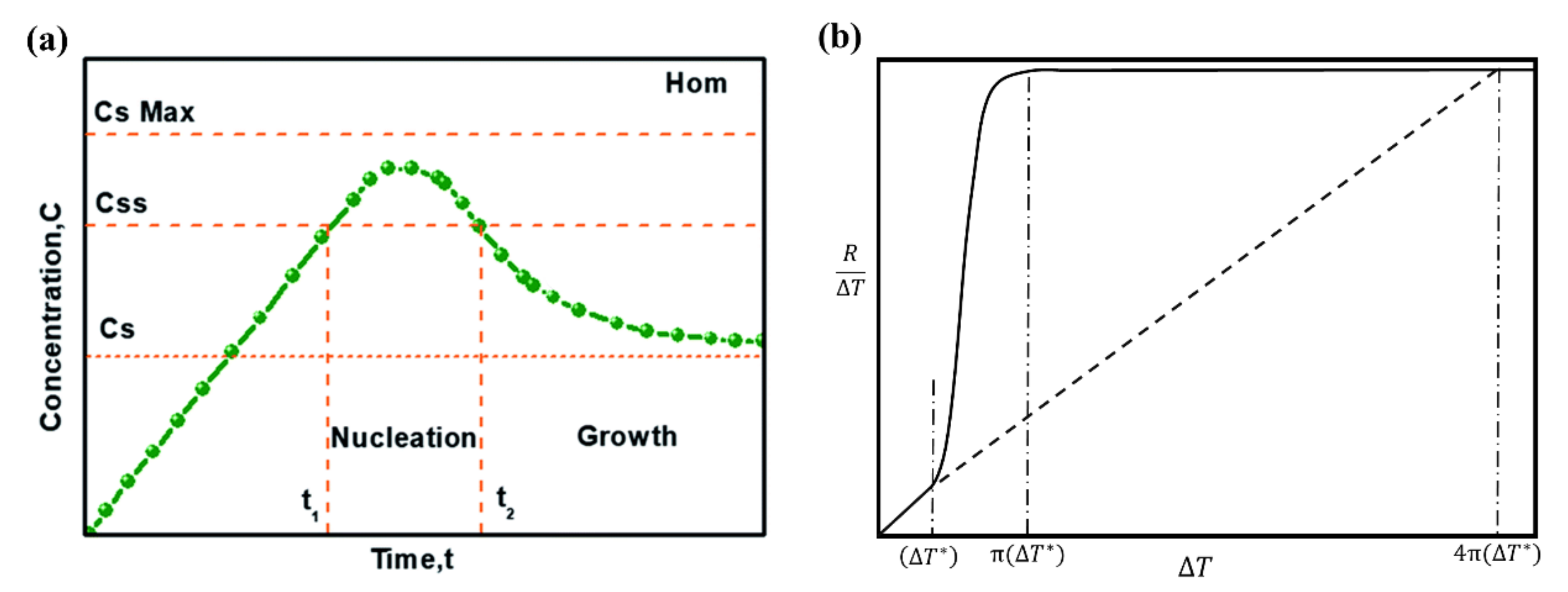
In the nucleation section, we invoke the LaMer diagram, which is mainly used to describe the variation of the concentration of the perovskite precursor (C) with the time (t) at a constant isothermal solvent evaporation rate (Figure 3a) [44]. There are three main stages in the LaMer diagram. In the first stage, the precursor concentration C increases linearly with time up to a supersaturation limit (Css), and the value of Css will not exceed the critical supersaturation limit (Cs Max). The second stage is an oversaturated environment, where the nuclei will generate. The generation of crystal nuclei consumes the solute, and C will fall below to Css. At this stage, the nucleation time is closely related to the nucleation density. When t becomes longer, the generation rate of nuclei decreases, resulting in a low nucleation density. A large number of crystal nuclei can be generated rapidly when t is short. Obtaining a high density of homogeneous nuclei during the nucleation stage is favorable for the growth quality of the crystal. The film will form isolated “islands” at low nuclei densities, which may not coalesce at the end of growth. Accordingly, the time interval t1–t2 in the second stage should be shortened to ensure the explosion of the number of crystal nuclei. In the third stage, the crystal growth will occur, which will end when the concentration of the precursor solution decreases to the solubility limit (Cs). It should be noted that although the LaMer diagram is used for homogeneous nucleation, the researchers believe that it can also be employed for the heterogeneous nucleation of perovskites, since heterogeneous nucleation occurs in C ≪ Css [45,46].
3.2. Crystal Growth
We suggested that the film was amorphous after spin-coating the precursor solution, which could be regarded as the liquid in undercooling. During the growth of perovskite, there was a transition region at the liquid–solid interface, where the dynamic process of disorder-to-order structural transformation took place. An interfacial diffusion model can be used to describe this process [48]. The interface would move through a periodic potential field corresponding to the periodicity of the lattice, and the interface energy will also change through the periodicity. The relative amplitude of its interfacial energy is described by m:
The interface energy changes with α to the value of
where n is the number of atomic layers contained in the interface transition region, α is the interface position, and a is the atomic layer spacing in the direction perpendicular to the dense row surface.
The energy at the interface during crystallization varies periodically, and the change in its free energy at a distance of movement of δα is
where G is the free energy, and is the value of the interface energy.
The condition for the absence of the potential barrier during interface growth is δG = 0, so . Bringing (1) into the calculation, the critical driving force for continuous growth to occur can be derived as
where ΔT* is the critical degree of undercooling Hm is the enthalpy of fusion, Tm is the melting point, and Vm is the molar volume.
During the forward movement of the crystalline interface, if the growth drive is small, the change in interfacial energy is essentially periodic as it approaches equilibrium. When the growth drive is large, the interfacial potential barrier to be crossed for crystal growth decreases. When the growth drive reaches a critical value, the interfacial potential barrier that needs to be crossed for crystal growth is 0. At this point, the growth interface will follow a continuous growth pattern and the interface is completely rough, regardless of the absolute value of the interfacial energy. Thus, the value of the driving force in crystal crystallization determines the quality of the interfacial growth.
The driving force required during the transition of the crystal from phase α to phase β is
where ΔT is the degree of undercooling in growth, ΔHα−β is the enthalpy change during the transition, and Th is the temperature at the point of phase change. The driving force that drives the crystal growth transition is determined by the internal degree of undercooling.
The rate of crystal growth at a given value of degree of undercooling is
where μ and b are kinetic constants [49].
The relationship between the rate of crystal growth and the driving force can be replaced by the relationship between the rate and the degree of undercooling (Figure 3b) [47]. At the low undercooling ΔT < ΔT*, the crystal growth rate is small, and the crystallization process occurs in a step-growth mode. When the ΔT* < ΔT < πΔT*, it is the transition regime, where crystallization is “mock-lateral” growth. The growth rate is faster and will no longer change with increasing undercooling when the undercooling exceeds ; the crystallization is a continuous mode, and the interface is completely rough. Thus, the crystallization can be controlled by adjusting the undercooling in the perovskite film.
According to the theory, the film grows along the crystal face [50]. We set the distance between two low index crystal faces as l, and the time for one face to grow to the other as t, so the growth rate can be expressed as
The ΔT* from Equation (5) is applied to Equation (10), where the relationship between crystallization time and undercooling can be obtained. When t > , the crystallization process is in step-growth mode. The crystallization is “mock-lateral” growth when < t <. When the crystallization time becomes faster, t < , the interface in continuous growth mode is completely rough, which is harmful for the carrier transport of the device. Therefore, during annealing, an appropriate reduction of the driving force and a longer crystallization time has a positive impact on the crystallization quality.
In general, we have summarized that there are two ways to improve perovskite growth: (1) the fast nucleation, which can guarantee the high coverage of film; and (2) the slow crystallization, which modifies the roughness and grain size. Regarding the annealing process, many studies have applied these two strategies to control the quality of crystals, which we will discuss more in the following sections.
4. Annealing Methods
In this section, we will discuss the popular annealing methods that comprehensively exist in PSCs. In order to systematically summarize and analyze the various annealing methods, we have divided the annealing methods into two main categories—physical annealing and chemical annealing.
4.1. Physical Annealing
Physical annealing primarily uses electromagnetic waves, thermal energy, ultrasonics, pressure and other physical strategies to promote precursor reactions and crystallization of perovskite [18,51,52]. Physical annealing is mostly non-direct contact annealing, which reduces the possibility of introducing impurities. This method is also environmentally friendly, which is a suitable annealing strategy for future commercial fabrication.
4.1.1. Thermal Annealing
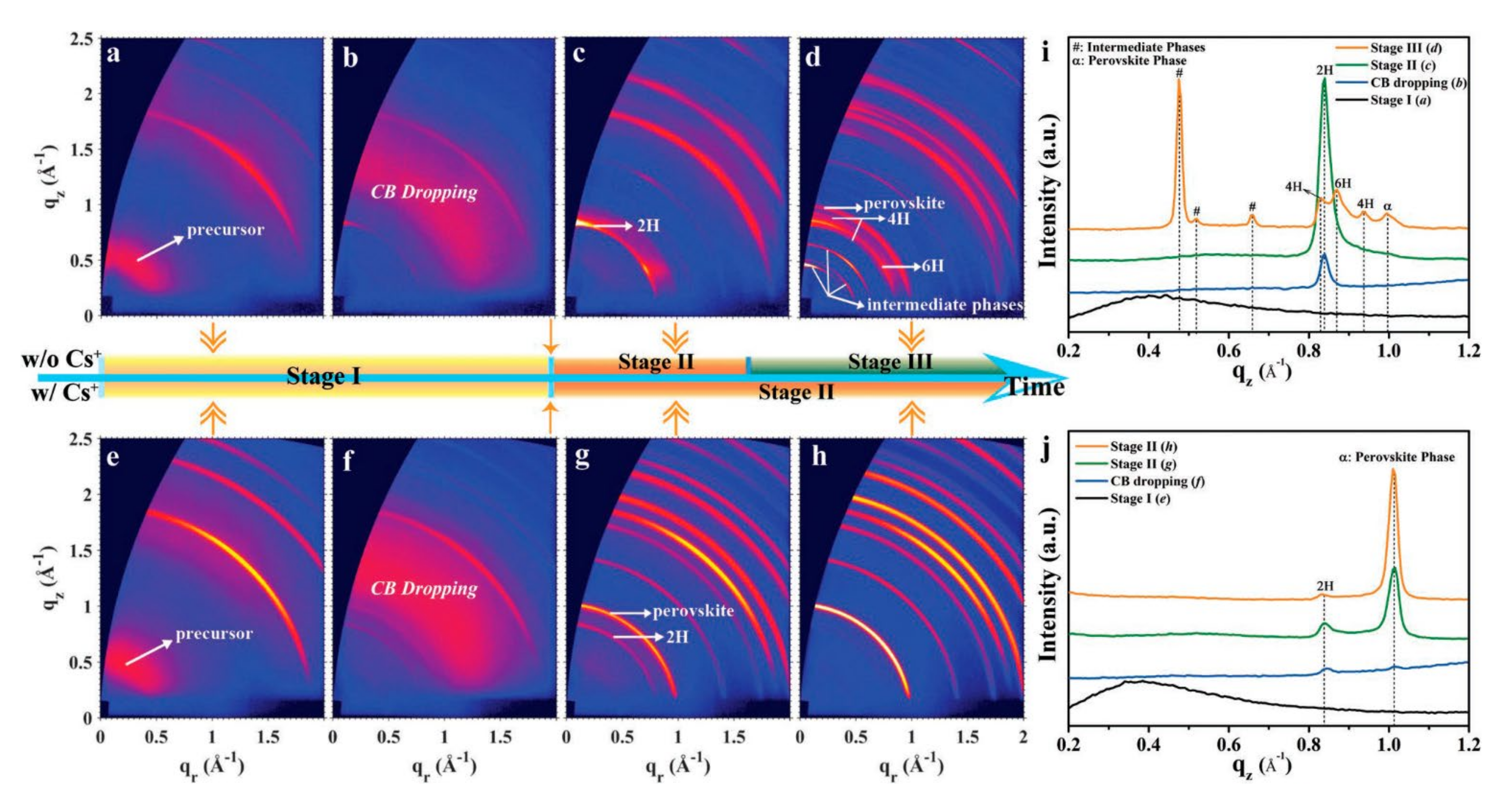
Direct thermal annealing of the substrate after spin-coating the precursor solution is the extensive method used by numerous researchers to crystallize perovskite as its convenience and simplicity [18,53,54]. During thermal treatment, the researcher found there was an annealing window, which would strongly enhance the crystallinity of perovskite film. The choice of thermal annealing window in crystallization was significant for the growth of the crystals [55,56,57]. The mixed halide perovskites (Csx(FA0.83MA0.17)1−xPb(I0.83Br0.17)3) had three stages during the film growth process, which contained different crystal phases (Figure 4) [56].
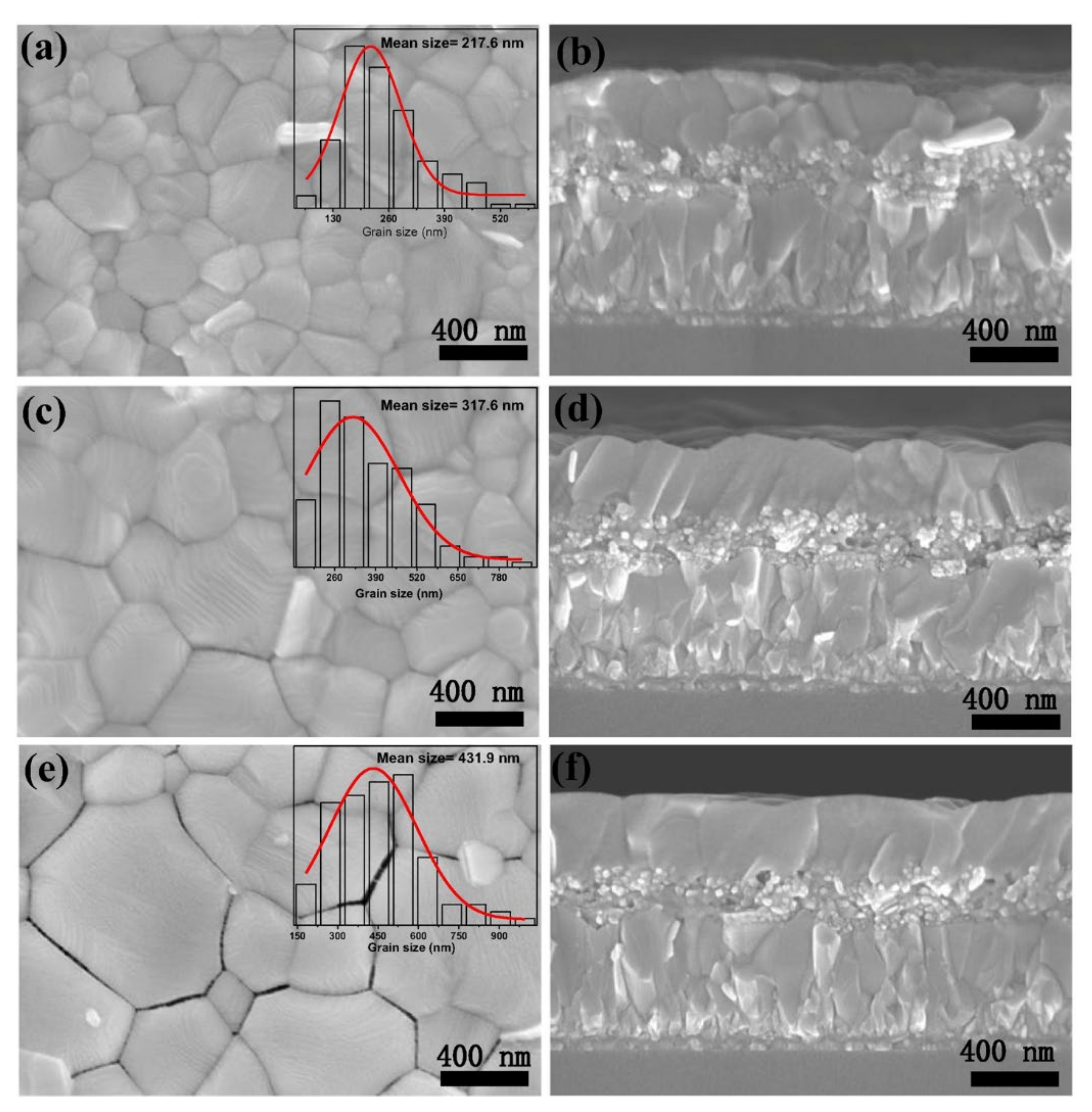
Stage I was the precursor solution period; stage II was the main δ-phase (2H); and stage III contained the multiple complex phases, including two hexagonal polytypes (4H, 6H), CH3NH3I (MAI)–PbI2–Dimethyl sulfoxide (DMSO) intermediate phases and the α-phase. The crystalline phase of the perovskite showed stronger diffraction intensities and orientations when annealing at stage II, suggesting an internally stable and symmetrical structure. Actually, choosing to anneal within the annealing window could avoid the formation of hexagonal polytypes during the perovskite crystallization process. Furthermore, the annealing window can be extended by additional ions [55]. The time and temperature of the thermal annealing determines the quality of the crystals. The results of Huang et al. showed that the initial phase formed at 105 °C for 10 min, and the crystallinity and grain size continued to increase after 2 h of annealing [53]. However, prolonged thermal annealing may lead to decomposition of the film and device stability due to the fragility of the perovskite structure [58]. Some researchers have used high temperature rapid crystallization to solve the problem of long annealing times [18,59,60]. Annealing at high temperatures in a short time could induce the removal of solvent to build a supersaturation condition, which would accelerate the perovskite nucleation and improve the density of the nucleus [18]. Wei et al. demonstrated that annealing temperature played a key role in controlling the coarsening of the perovskite grains. The grain boundary was almost perpendicular to the substrate as the film was treated at 250 °C for 10 s (Figure 5).
Annealing at 400 °C for 4 s could also acquire a grain size of 1 [59], which improved the carrier transport properties. This instantaneous annealing of crystallization was attractive for industrial production, but it may come at the expense of some crystal quality. In fact, the fast evaporation rate of organic solvents led to the dramatic shrinkage of the grains. In addition, perovskite appeared turbid in scattered light due to the rough film, which was worse at higher temperatures [61]. Annealing immediately after spin-coating the precursor solution causes rapid volume shrinkage and the solute does not have enough time to diffuse, causing the rough surfaces and continuous cracking at grain boundaries.
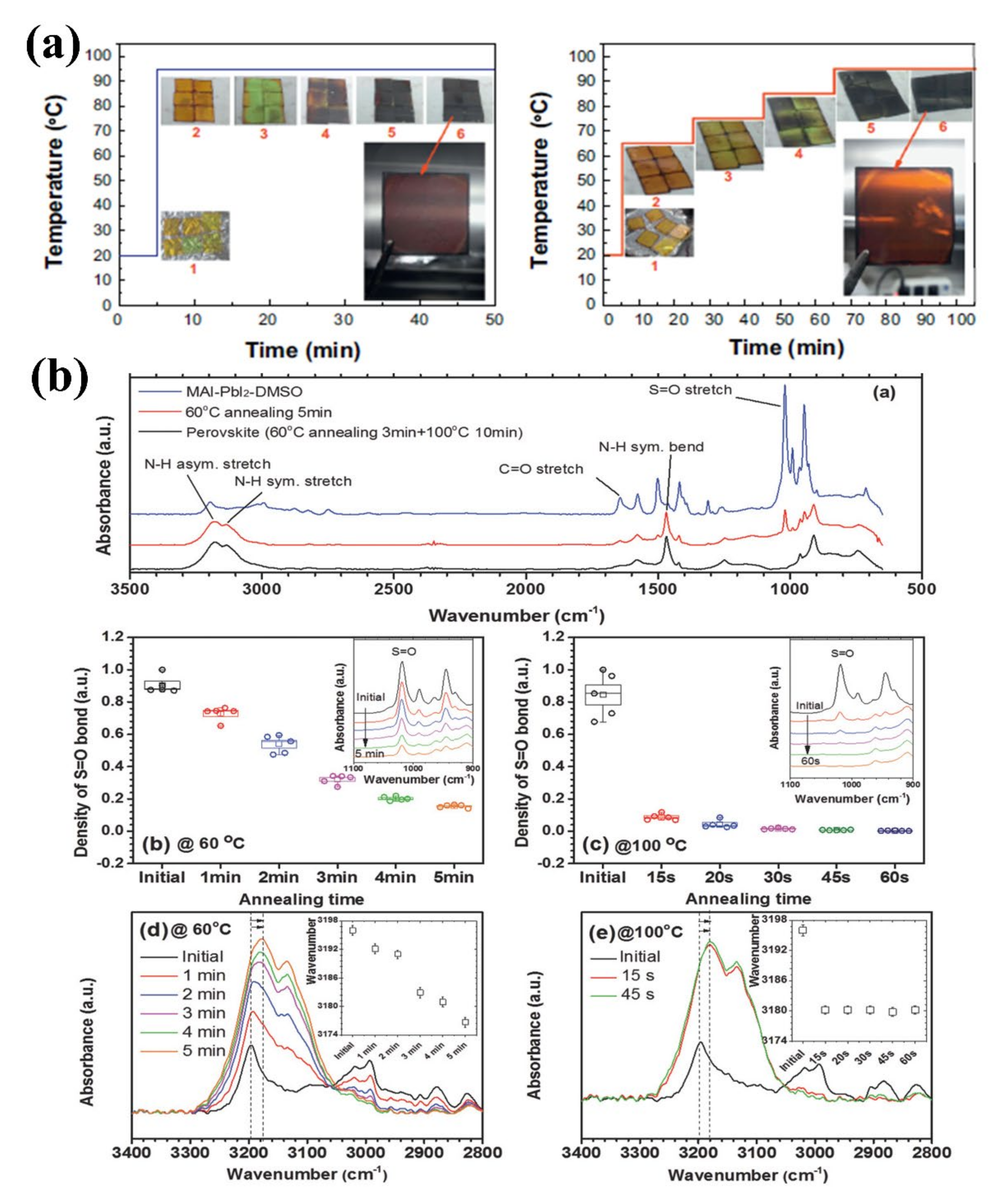
Therefore, considering the fact that a slower evaporation rate could both reduce the crystallization rate and improve the quality of the crystals [54], gradient thermal annealing has been found to be an effective way to reduce the evaporation rate of organic reagents and slow down the crystallization process of films [54,62,63,64,65,66]. A demonstration of the morphology change of perovskite films with gradient annealing and thermal annealing is shown in Figure 6a [62]. The film changed from yellow to black more slowly under the gradient annealing mode compared to direct annealing, which indicated a slower crystallization rate. It was demonstrated that gradient annealing was successful in slowing down the growth rate of perovskite. The evolution process of the internal chemical bonds in perovskite films reveals the changes of the internal substances under gradient annealing at the microscopic scale (shown in Figure 6b) [63]. The flourier transform infrared spectroscopy (FTIR) results displayed the gradual but slow transition from the MAI-PbI2-DMSO intermediate phase to MAPbI3 within the first 5 min of preheating at 60 °C, with a slow rate of DMSO dissociation and hydrogen bond formation between MAI and PbI2, while direct thermal annealing completed 90% of the DMSO release and hydrogen bond formation in 15 s. The main methods to improve the crystal quality are the control of nucleation and reducing the crystallization rate. The combination of the two methods has been shown to exhibit superior crystallization quality improvement compared to a single treatment [67,68].
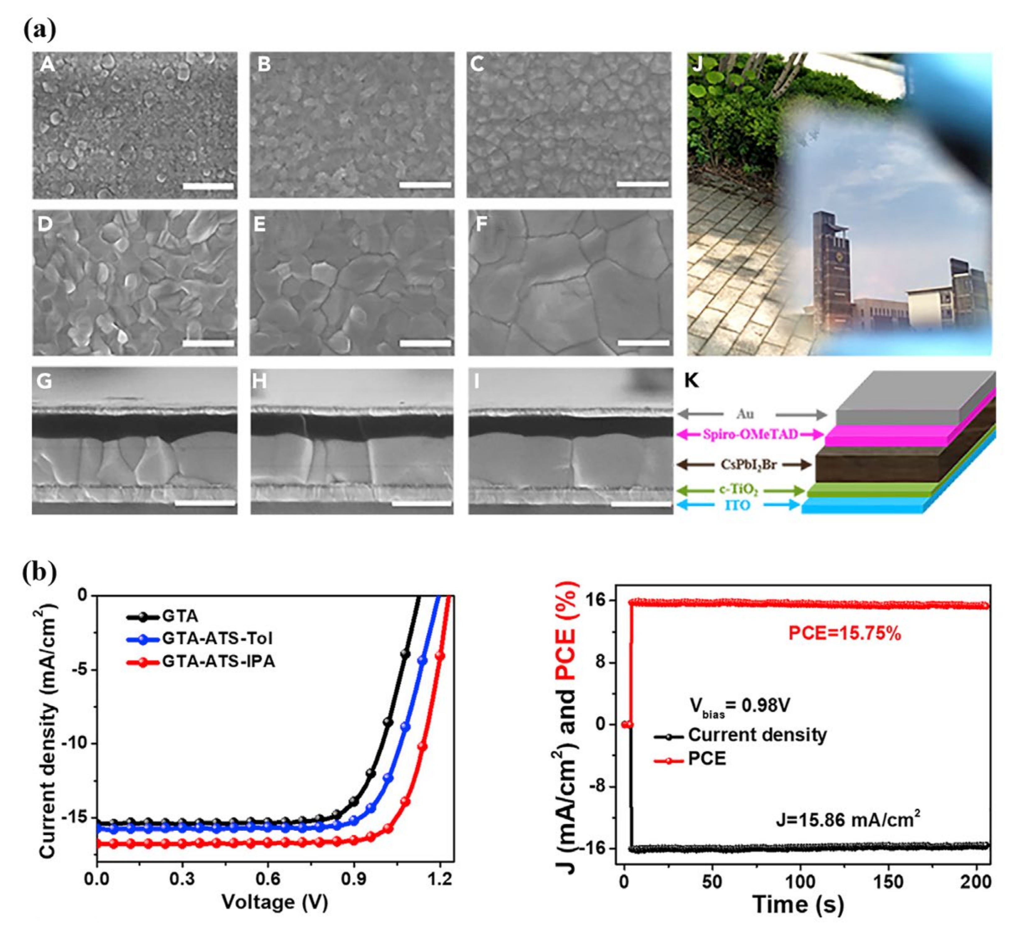
Li et al. combined gradient thermal annealing (GTA) with anti-solvent (ATS) engineering to precisely control the growth process of perovskite [67]. Organic solvents were taken as the anti-solvent to extract DMSO, in order to disperse the nuclei and homogeneously “freeze” the perovskite precursor onto the substrate. Then, the films would crystallize under the gradient annealing mode. As isopropyl alcohol (IPA) could extract the residual DMSO and had a weak coordination interaction with the CsPbI2Br precursor, the IPA improved the surface morphology of films more obviously than toluene (Tol). The grain boundaries of the perovskite prepared by the hybrid engineering were significantly reduced: the grain sizes exceeded 1 μm and the film surface was very smooth like a mirror (Figure 7). The devices achieved an efficiency of 15.7%, and the wet stability and ultraviolet (UV) stability of the device were also improved.
4.1.2. Electromagnetic Wave Annealing
Electromagnetic waves can radiate energy which have been used in many fields for heating, information transmission, etc. [69,70,71]. In the fabrication of perovskite, the main electromagnetic waves that have been used in the perovskite annealing process are infrared light waves, visible light, lasers and microwaves [52,72,73]. The intense pulsed light is a non-contact rapid heating method which can offer fast millisecond pulses of broad spectrum light (190–1100 nm) from xenon lamps [74]. Xenon lamps are used to provide high-energy pulse light to 150 J/cm2 for perovskite annealing, and can achieve thin film crystallization at the millisecond scale [54,70,75,76,77,78,79]. Druffel et al. successfully employed intense pulsed light generated by a xenon lamp to sintering of MAPbI3 on a mesoporous TiO2 substrate for first time [76]. The perovskites were subjected to 2000 J of energy in 2 ms. The films reached temperatures of 350–425 °C during the short-term heating and cooled to 100 °C within 3 ms, as the simulations displayed [80]. The extremely short times may result in the incomplete growth of the film surface, and the conversion of perovskite at the millisecond level was still lower than that of thermal treatment. In actual fact, studies showed that appropriately extending the pulse time to increase grain growth time under intense light could lead to better film coverage and higher performance devices [78]. The addition of light-absorbing material can improve the reaction rate of perovskite. The diiodomethane (CH2I2) additive can also improve surface coverage during rapid crystallization and enhance carrier transport [70]. The intense pulse annealing with halogen lamps was compatible with roll-to-roll manufacturing, which enabled production speeds of 26 m/min [77].
In the fabrication of perovskite films, infrared light can effectively promote precursor reactions and drive grain growth [72,80,81,82,83,84,85,86,87,88,89,90]. Infrared light is an electromagnetic wave with a frequency between microwave and visible light. The application of infrared light for annealing treatments mainly utilizes its ability to provide a large amount of energy in a short amount of time [83,84].
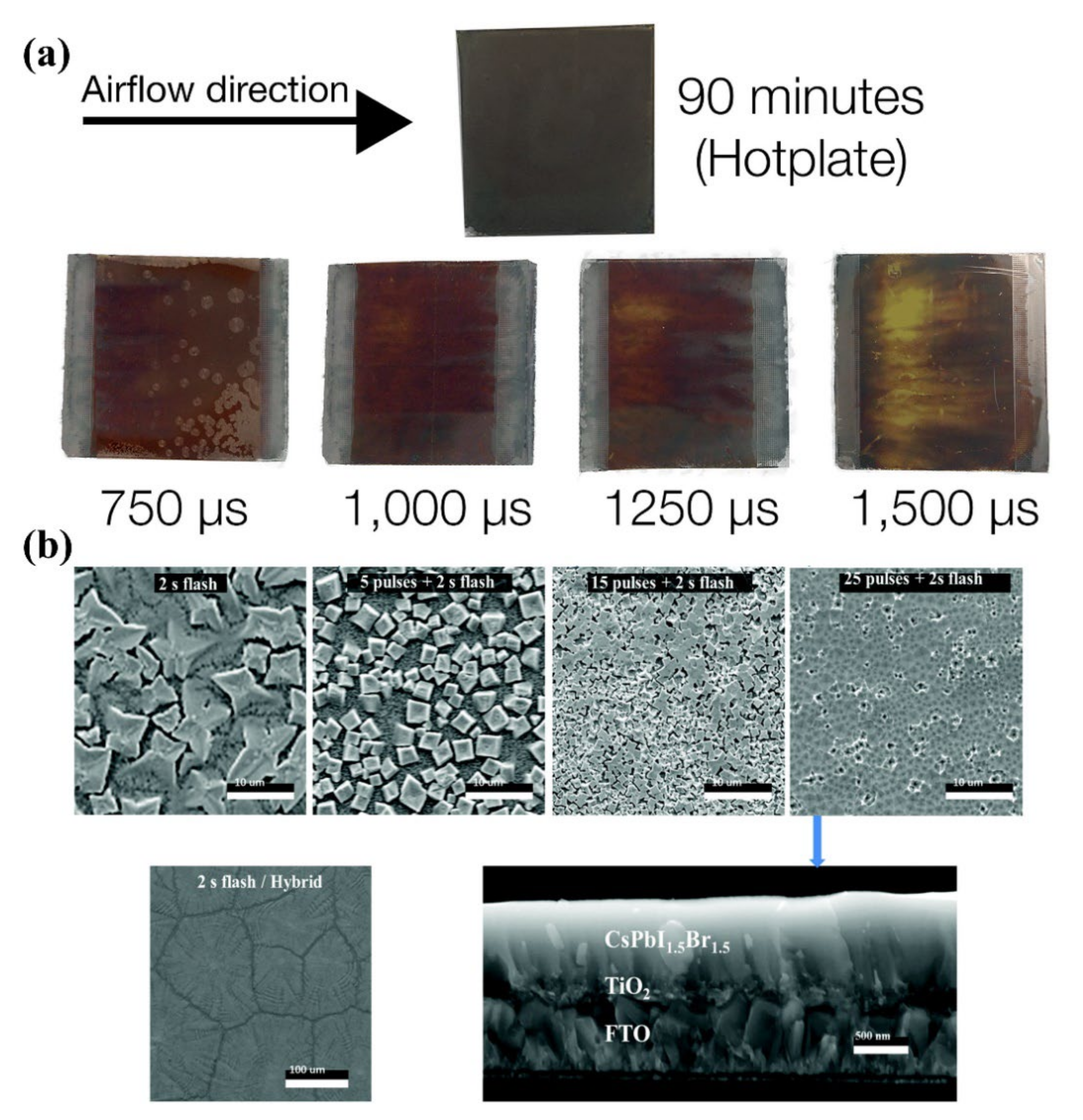
Watson et al. applied flash near infrared annealing to the crystallization of mixed-phase perovskite films for the first time [90], which reduced the crystallization time from 45 min to 2.5 s, revealing the amazing ability of infrared light in the annealing process. In a further study, the addition of mesoporous Al2O3 to the c-TiO2 substrate again reduced the annealing time to 1 ms [81]. The growth of films under flash annealing at 500 V lamp voltage, as well as a film annealed in a hotplate, are both shown in Figure 8a. The film surface obtained great growth at 1 ms, but the flash annealed perovskite displayed a lighter color compared to the thermal treatment and a poor uniformity of coverage, which might lead to a decrease in absorbance and low efficiency of the device. The effect of pulses on driven crystallization in flash infrared annealing was investigated by Abate et al. [82]. The nuclei gradually fused and grew from isolated material to sheet-like films as the number of pulses and flashes increased (Figure 8b). Pulsed flash infrared annealing provided precise control of the kinetic process of perovskite nucleation [87,89]. The crystal growth rate and solute concentration determines the grain size of the grain boundaries in flash annealing [85], and the carriers at the grain boundary edges exhibited longer electronic lifetimes. Gradient flash annealing has also been confirmed to provide a significant improvement on crystalline quality [75]. This approach achieved better performance by retarding crystallization, regulating the atomic diffusion rate, and controlling the sufficient evaporation between each flashing.
Providing a large amount of energy in a short time to achieve rapid annealing has potential for future industrial production. However, according to the principles of crystal crystallization, the fast crystallization rate resulted in a poorer crystal quality and may also introduce greater stresses, leading to problems in the subsequent stable operation of the device [54].
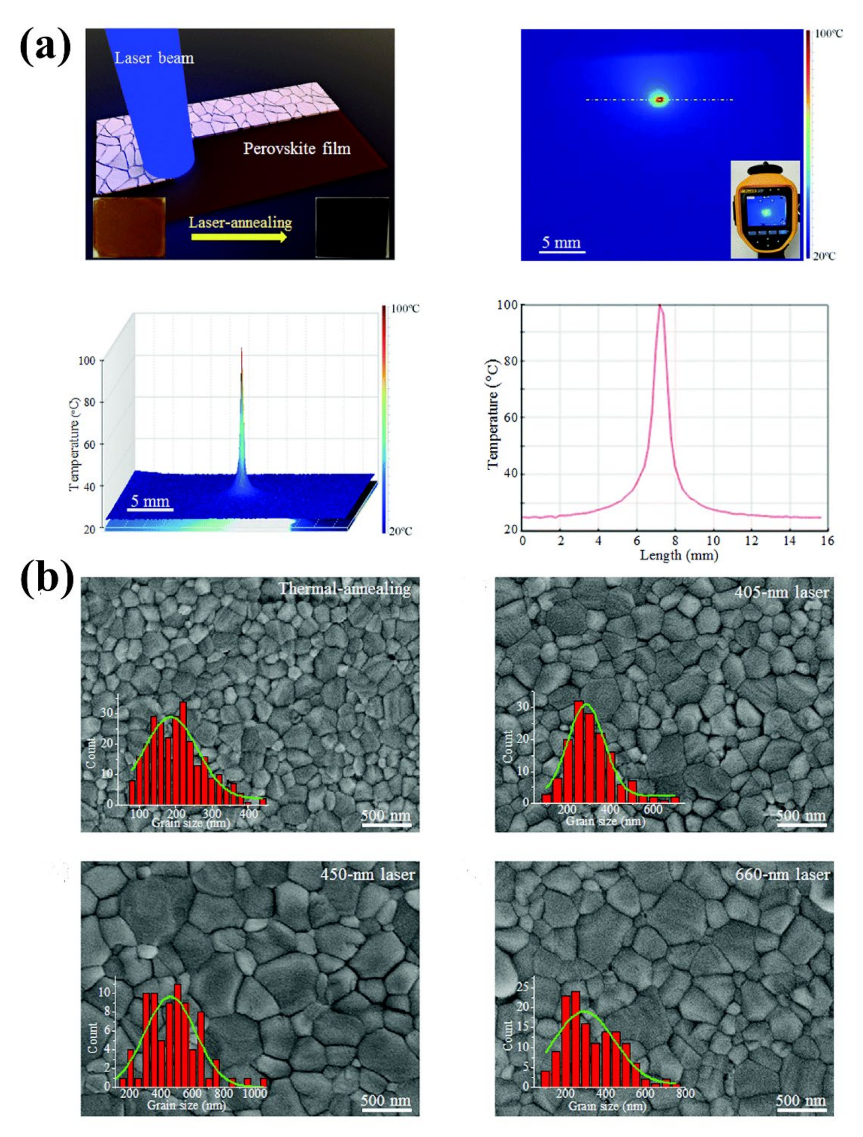
Lasers can provide a great strategy for modulating the crystallinity and electrical properties of films due to their high energy and excellent monochromatic characteristics, and are widely used in the fabrication of perovskite layers, such as the electron transport layer TiO2, the hole transport layer NiO, and the electrodes [73,91,92,93]. Lasers also perform well in the promotion of crystallization of the functional layers [23,94,95,96,97,98,99]. Compared to the pulsed light annealing discussed above, the laser had a remarkable ability to promote crystallization, and the efficiency of the device exceeded 20% [23]. The laser spot was scanned at a speed under the control of the program that produced a maximum temperature of 100 °C on the film surface (Figure 9a). Results from other researchers’ simulations also showed that the laser can generate temperatures of over 100 °C inside the film [94]. The films had superior crystallinity and orientation in the laser-driven mode. In addition, different wavelengths of laser light had different impacts on the growth of the films. The grains had a better grain size at 450 nm, probably due to the high absorption of perovskite at short wavelengths in the non-UV (Figure 9b). The researchers believed that the localized temperature gradient created by the laser at the perovskite grain boundaries would allow larger grains to absorb more energy and have higher temperatures than smaller grains, thus inducing selective growth of larger grains. The energy received by the film per unit time was related to the out-of-focus distance of the laser and the scanning speed, which would affect the properties of the crystal. The band gap narrowed under laser annealing and the PL peak was red-shifted [98]. In the laser approach, there is an inverse relationship between the scan speed and energy density. After receiving higher energy density in the low-speed mode of laser crystallization, the interaction between the organic cation and the inorganic frameworks of the film was enhanced, which resulted in the right shift in the conduction bands (CB) and valence bands (VB). The study also found that the conductivity of the perovskite surface would convert from P-type to N-type as the scan speed changed from high to low, which might be due to an increase in the conversion of perovskite. The laser annealing had a significant effect on stresses in thin film growth, where it can reduce tensile stresses during growth [96,98]. Regular thermal treatments will generate high tensile stresses within the film [100,101], causing perovskite to decompose, and promoting the formation of numerous defects, which adversely affected the carrier transport of defect trapping. The reduction in stress release comes from the fact that the laser enhanced ultrafast diffusion in the perovskite films. The 40% stress was reduced in the film by the laser, and the degradation rate of the film was cut down by more than two times at 80% humidity [96]. Laser annealing was equally applicable to flexible polymer substrates, which protected other functional layers from damage in the fabrication of flexible PSCs [94]. In addition, the compatibility between the different transport layers and the laser annealed film should also be taken into account for improving the device efficiency [95].
UV has been considered detrimental to perovskite films due to its ability to break down the active components within the perovskite [102,103]. However, utilizing the high absorption of perovskite in the UV band appropriately can promote crystallization. Li et al. applied a 365 nm UV light emitting diode (LED) to achieve the accurate annealing of the perovskite layer by controlled UV light irradiation [104], which significantly eliminated the hysteresis effect and obtained a device with an efficiency of 19%. UV light can be annealed by controlling the amount of irradiation. Therefore, we suggested that the wavelengths in the various types of light annealing might be extended to the UV band to improve energy utilization rate and reduce the consumption.
Microwaves are part of the electromagnetic wave, with a wavelength ranging from 1 m to 1 mm, which commonly converts energy from electromagnetic energy to thermal energy rather than heat transfer [105,106,107]. Several studies have demonstrated that microwaves also convey excellent control of perovskite crystallization [108,109,110,111].
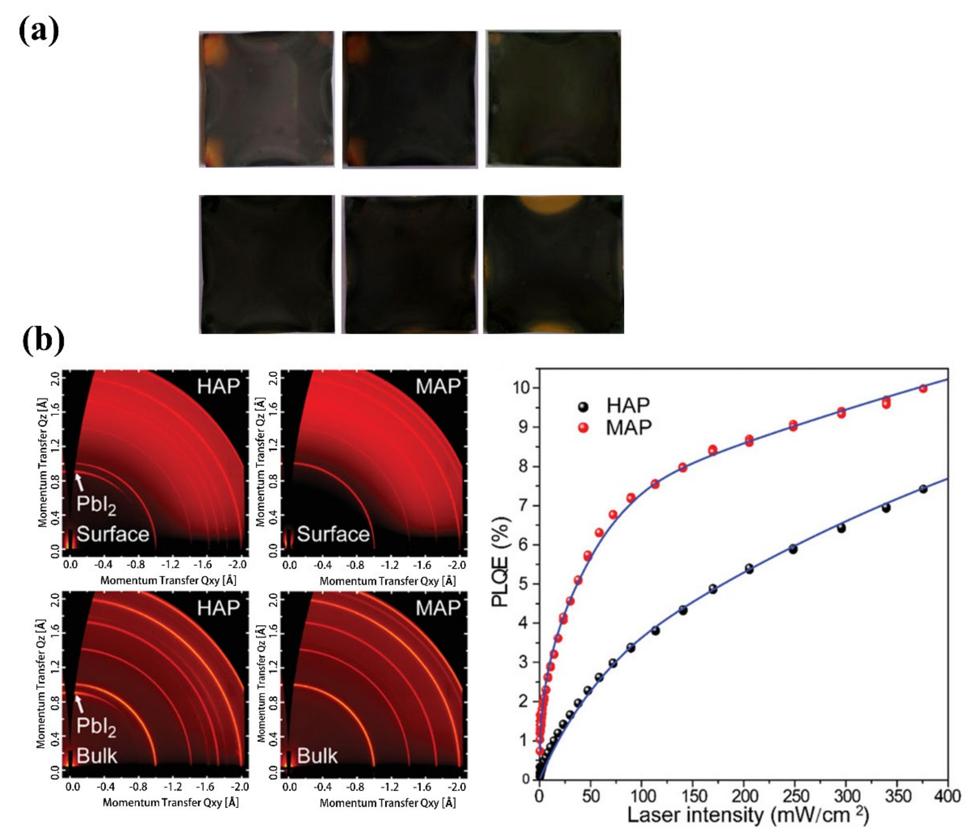
The evolutions of the color when the perovskite films were exposed to microwave irradiation for various times is presented in Figure 10a [108]. The microwave produced different temperatures in the film in different areas of the film. At the initial stage, the four right angles of the sample were yellow, showing a hysteresis in growth compared to the central region. The results of Huang et al. revealed that this temperature difference in various regions did not seem to have a significant effect on the crystallization and photoluminescence quantum efficiencies (PLQEs) of perovskite in Figure 10b [109]. Compared with heat treatment, microwaves can effectively accelerate the reaction of MAI and PbI2 at the surface and in bulk, which played a uniform role in the whole film, and the impurity phase was effectively controlled.
However, there was no definitive conclusion on the growth mechanism of perovskite under microwaves. Mascarenhas concluded that microwaves made the internal polar solvent N,N-Dimethylformamide (DMF) and DMSO dipole vibrate at high frequencies, and then generated heat to crystallize the perovskite film rapidly [110]. This was supported by the phenomenon that only the perovskite powders that contained DMF or DMSO solvents turned black under microwave irradiation [112]. Other studies attributed the crystallization effect to the absorption of microwaves by the substrate, which drove the crystallization of the film [108]. A third explanation has suggested that the dipolar polarization and conductive mechanisms worked together, and were responsible for the controllable crystallization of perovskites films [110].
4.1.3. Ultrasonic Annealing
Ultrasonically induced crystallization is also an alternative to heat treatment as an annealing method. Eslamian et al. used ultrasound to induce crystallization for 3 min after spin-coating the precursor solution, and obtained an efficiency of 14.09% [113]. Zhang et al. prepared the device with an efficiency of over 17% at room temperature by using ultrasound at 40 kHz [114]. Ultrasonically induced growth is cold processing, which is a viable crystallization method for the processing of flexible cells. Due to the simplicity of ultrasonic equipment, ultrasonics can be used in subsequent large area preparation processes such as spraying, blade and slot die coating processes.
4.1.4. Pressure Annealing
Pressure is a universal and controllable thermodynamic variable that can be used to alter the electronic structure and properties of materials [115,116,117,118]. In the growth of perovskite, the addition of pressure could achieve regulation of film crystallization, which can obviously improve the grain size of perovskite, crystallinity, stability under humidity, and defect density [7,119,120,121]. The role of pressure in perovskite crystallization was mainly employed to regulate the evaporation and sublimation of volatiles, and thus improve the quality of crystals [51].
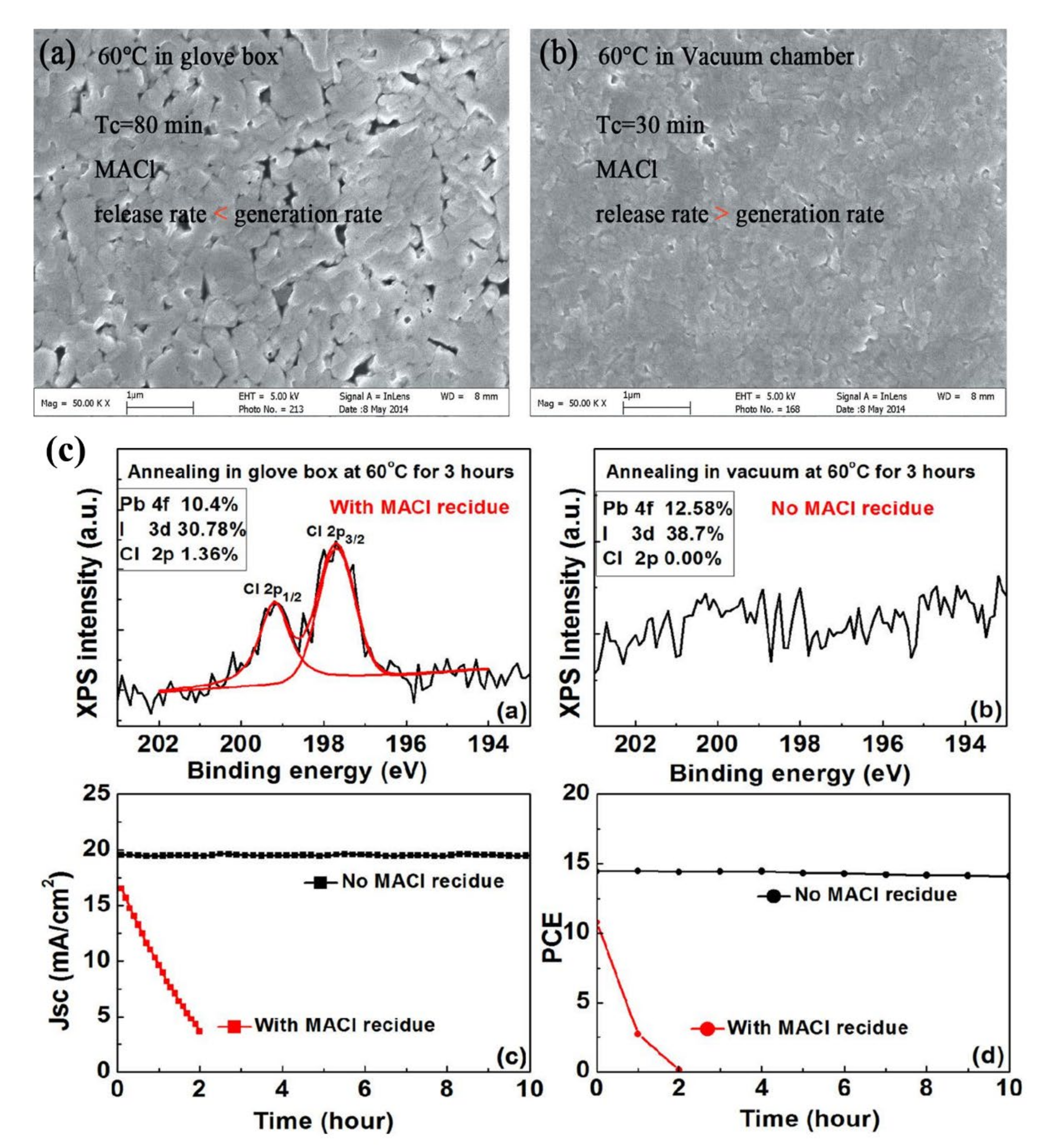
The average grain size of the films increased with various pressures under low pressure conditions. The nucleation and grain growth process were mainly influenced by the annealing pressure and time [121]. The films displayed great coverage under vacuum conditions due to the control of the volatilization rate of byproducts by vacuum-assisted annealing (shown in Figure 11a,b) [7]. The vacuum environment reduced the sublimation conditions of CH3NH3Cl (MACl), resulting in a release rate of byproducts greater than the production rate. The stability of the device in air was enhanced due to the complete removal of MACl by vacuum-assisted annealing (Figure 11c). Other studies also demonstrated that MACl was more easily removed within the vacuum compared to an atmosphere of nitrogen [119]. The combination of vacuum-assisted thermal annealing and solvent–solvent engineering enabled inkjet printing of high-quality perovskite films [122]. Under high pressure, the growth of the film was likewise significantly influenced. Pressure annealing could achieve the modulation of the band gap, which caused an increase in the crystallinity and absorbance of the film [120,123]. Meanwhile, the crystallization rate of perovskite was faster under high pressure annealing conditions than in the atmosphere [124].
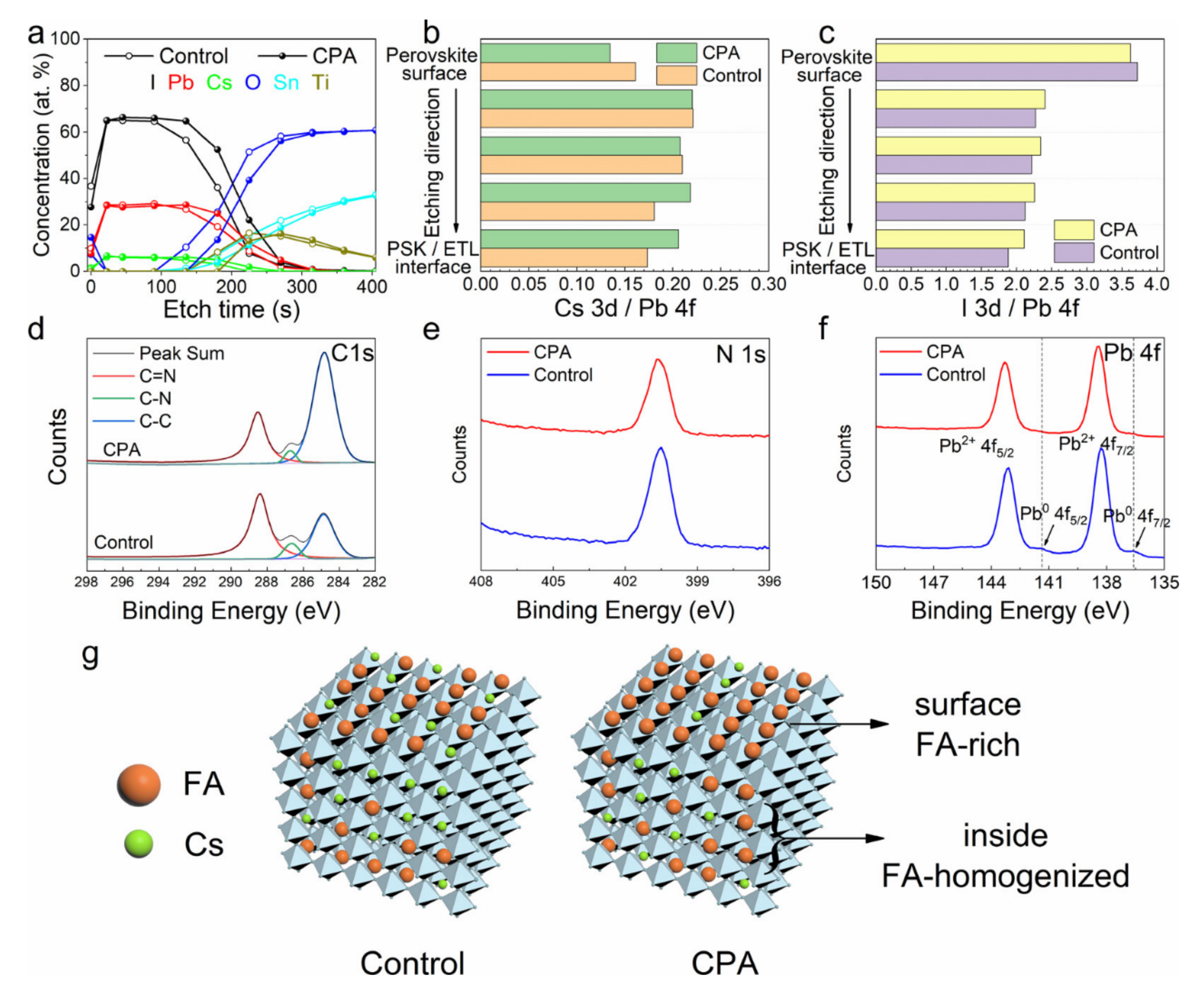
Interestingly, the results of several researchers have found that devices prepared by high pressure annealing have shown excellent stability [51,120,125]. Cheng et al. fabricated devices with excellent moisture and heat tolerance under high-pressure annealing, and the unencapsulated devices maintained 80% of their initial power conversion efficiency (PCE) after 30 days of aging at 100 °C and a relative humidity (RH) of 80% [51]. The improvement in device stability comes from the optimization in internal cation concentration under pressure annealing [125]. As depicted in the X-ray photoelectron spectroscopy (XPS) results, although the structure inside the film did not change much in confined-pressure annealing (CPA) and conventional annealing modes, the concentration of Pb2+ ions and A-site cations were more uniformly distributed in CPA, which led to a more stable crystal structure (Figure 12). Researchers believed that the variation of the A-site might be caused by the confined pressure environment that generated concentrated A-site species gas. According to Figure 12d,e, the increased intensity of the C-C bond on the film surface was responsible for the enhanced wet stability of the PSCs.
4.2. Chemical Annealing
We have defined chemical annealing as the addition of chemicals to assist crystallization during the annealing of perovskite or using chemical reagents to directly complete crystallization without thermal treatment. For example, the chemical reagents have been combined with traditional thermal treatments to improve the crystalline quality of the film by dissolving–recrystallizing the perovskite film, or reducing the evaporation of organic solvents [126,127]. On the other hand, researchers have used the principle of extracting polar solvents with organic reagents to achieve the supersaturated crystallization of perovskite, or have added ions into the precursor liquid to complete the coating and crystallization of the film at the same time [128,129].
4.2.1. Solvent Annealing
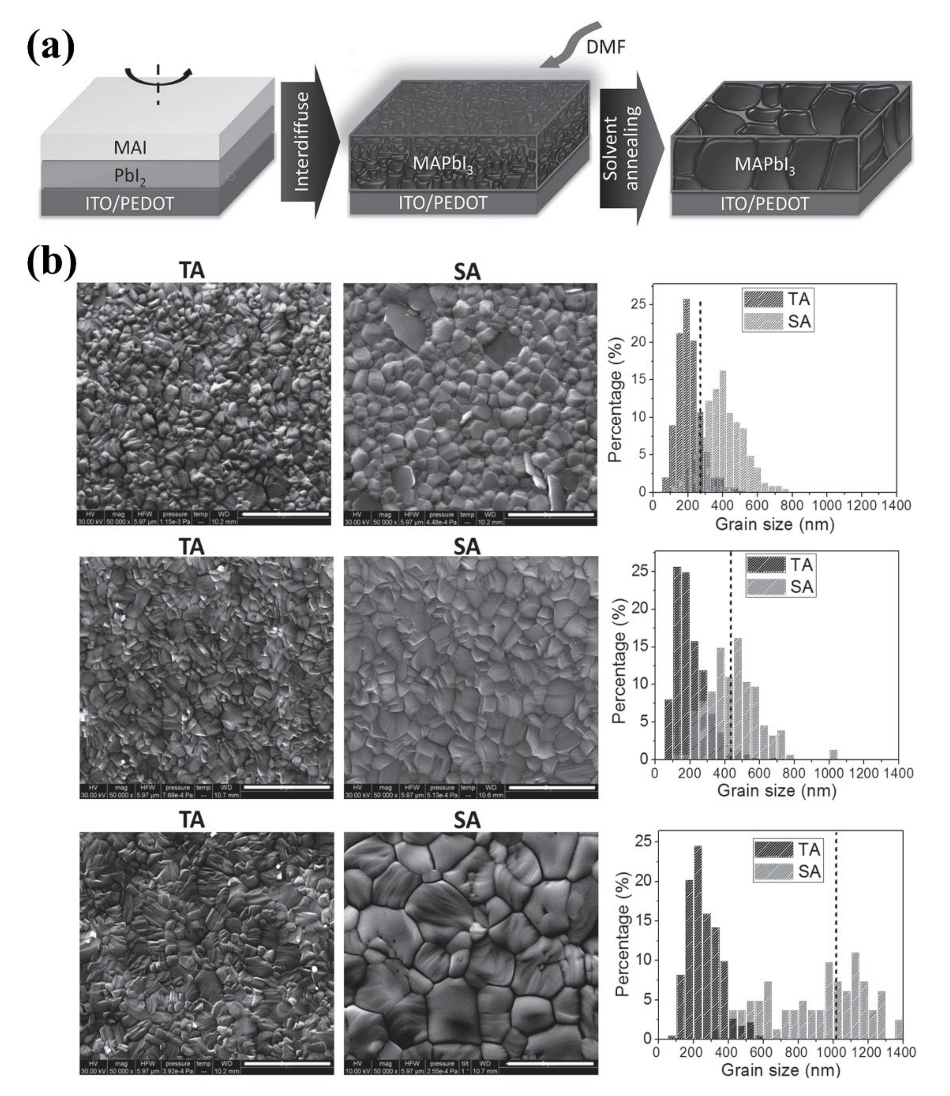
Solvent annealing for crystalline modulation is achieved by the addition of polar solvent vapor to the annealing [130,131,132,133,134,135,136,137]. Solvent annealing (SA) was first introduced to the perovskite crystallization by Huang et al. [21]. The organic polar solvent vapor provided a humid environment, and the high solubility of PbI2 and MAI in DMF vapor resulted in longer diffusion distances for precursor ions and molecules than in thermal annealing (TA), which promoted grain growth and produced larger grain sizes (Figure 13a).
The SEM results showed the remarkable contribution of the method to grain growth (Figure 13b). SA could form almost defect-free perovskite crystallites [138]. The electrical properties within the grain plane of the recrystallized grains were superior to grain boundaries within the grain plane. The conductive atomic force microscopy (c-AFM) results revealed that the peak current values for representative grains in SA (17 nA) were higher than those in TA (16 nA), indicating that the in-plane electrical properties of grains under recrystallization in a solvent atmosphere were superior to the grain boundaries [139]. The DMF solvent-annealed perovskite films also displayed a more prominent carrier recombination effect in the grain boundaries, which might account for the greater improvement in photoconductivity in the grain plane than in the boundaries in solvent annealing [140]. The concentration of DMF vapor needed to be reasonably controlled, as the excessive DMF vapor was a challenge to the photovoltaic performance of the film [141]. DMF and DMSO have already become the most widely considered choices in many solvents due to their significant dissolution–recrystallization effects and their ease of removal from perovskite films [126,132,134,139,140,141,142,143,144]. DMSO solvent annealing also had an excellent ability to form grains with low defect density. However, unlike DMF annealing, the DMSO-treated films showed a blue-shift in the photoluminescence peak; some studies attributed this phenomenon to an increase in band gap during the annealing process [145], while others suggested that the shift came from the relatively low trap density near the band edge [131]. The synergistic annealing of various solvents further improved the effect of single solvent annealing. A small amount DMSO added into DMF could regulate the growth by forming MAI-PbI2-DMSO intermediate phases with strong Lewis basicity, allowing extensive incorporation and the disappearance of grain boundaries [134]. Compared to single IPA or DMF annealing, mixed solvent annealing of DMF and IPA was superior in improving device stability and eliminating hysteresis effects [132]. In addition, DMF/DMSO mixed with chlorobenzene (CB), propanol, H2O, etc., were also applied to improve the crystalline quality [126,144]. Researchers have also developed some polar solvents to replace the organic solvents to achieve annealing, such as pyridine, CB, 1-Methyl-2-pyrrolidinone (NMP), etc. [146,147,148]. Alcohols such as methanol, ethanol, isopropanol, n-butanol and benzyl alcohol were applicable in solvent annealing engineering [149,150,151]. Alcohol annealing significantly suppressed the dark current and elevated the photocurrent, with methanol vapor becoming the most prominent in terms of high reproducibility and elimination of photocurrent hysteresis [149].
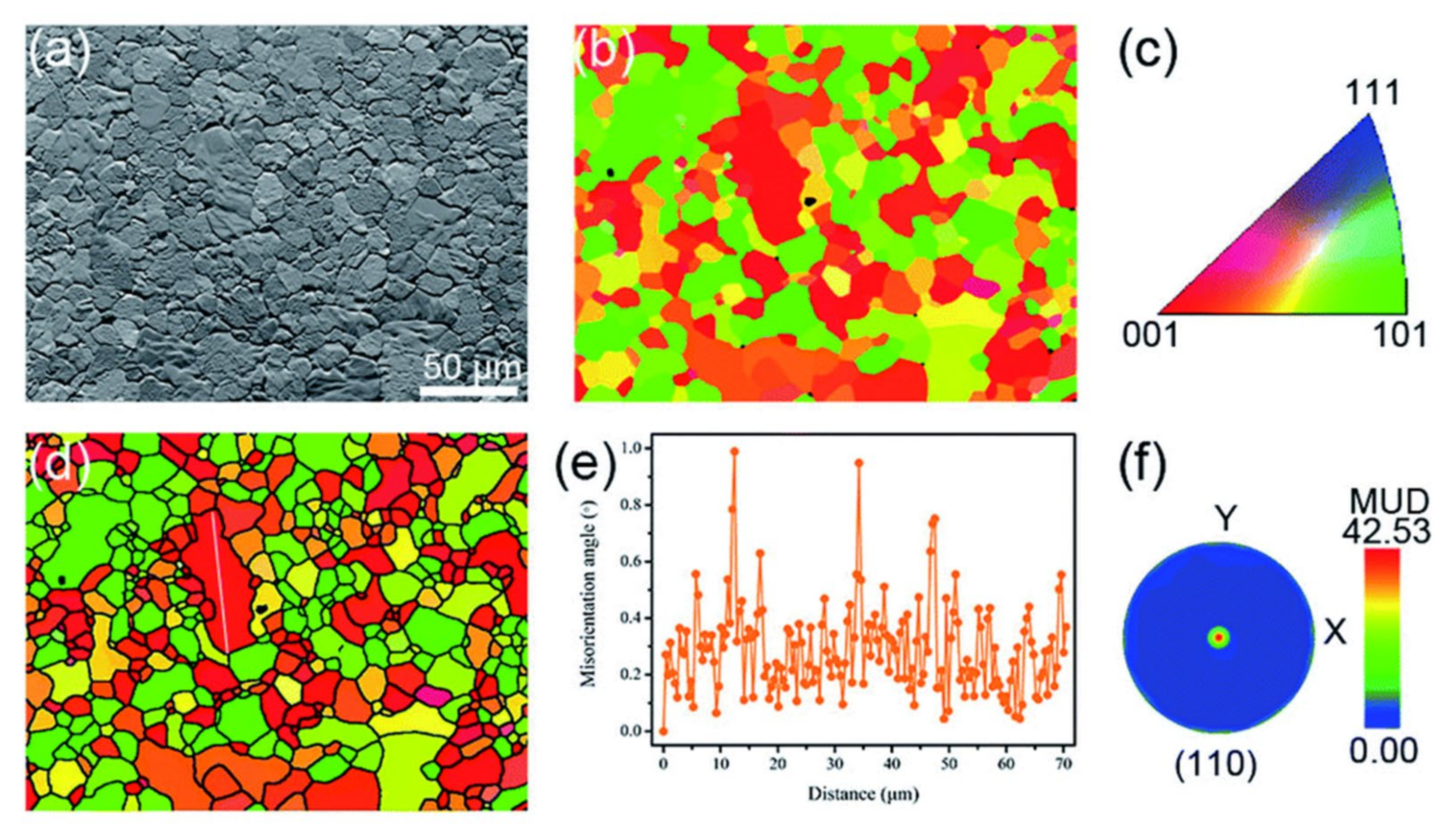
Methylamine-based chemical vapors also performed remarkably in inducing annealing in perovskite [152,153,154,155,156]. The methylamine vapors were annealed in the same solid–liquid–solid process as any other solvent annealing modes. In the fabrication of printable mesoscopic PSCs [153], methylamine improved the pore filling of perovskite in the mesoscopic structure, resulting in films with complete surface coverage and a high degree of crystallinity. The PbI2 would be distributed on the surface and grain boundaries of the film after methylamine vapor recrystallization, which passivated the internal defects. The addition of methylamine reduced the weave of the films with random grain orientations [152]. The backscattered electron (BSE) results of film revealed that the textured grains were well defined, with sizes ranging from 10 to 50 μm after methylamine annealing treatment (Figure 14a), and the X-axis inverse pole figure showed that the grain orientation under methylamine gas annealing was mainly concentrated in the (1,0,1) (0,0,1) plane. This method could effectively induce the growth of highly oriented and full-coverage films; methylamine was intrinsic to perovskite and there was no possibility of introducing excess impurities during the annealing process. Not only organic solvents but also water was confirmed to achieve self-healing of grains in annealing [157,158,159,160,161]. Snaith et al. demonstrated that moisture could solvate the methylammonium component and “self-heal” the perovskite lattice [158]. The films that annealed at high humidity showed higher photoluminescence quantum efficiency and carrier life due to the reduced density of traps. Moisture dissolved hygroscopic organics (formamide, methylammonium and possibly other components) during the annealing process and allowed them to effectively repair the perovskite structural domains or boundaries [161], filling any trap states created during the manufacturing process.
4.2.2. Solvent–Solvent Extraction Annealing
Perovskite films are driven to crystallization by an oversaturated environment created by the reduction of solvent. The solvent evaporation is reduced by normal heating in perovskite films, which is not optimal for the fabrication of flexible cells. Therefore, through the principle of mutual solubility of organic solvents, some researchers have chosen specific organic reagents to extract the polar solvent inside the film to drive crystallization [162,163,164,165]. Ether-based chemical materials were the most commonly used extractants, which had the characteristics of low polarity, stable properties, being less likely to react with airborne components, and a low boiling point [158,160]. Padture et al. proposed the use of diethyl ether (C2H5OC2H5) for induced crystallization [166]. The substrates were immersed in a room temperature bath of solvent diethyl ether for two minutes immediately after spin-coating the MAPbI3 precursor. The films were dried at room temperature to produce smooth films with a PCE of up to 15.2%. An additional anti-solvent treatment prior to immersion in ether (DDE) successfully enhanced the crystallinity of the extractive annealing, resulting in the device efficiency of 19.5% [162]. Anisole solutions had the superior ability to drive crystallization [164].
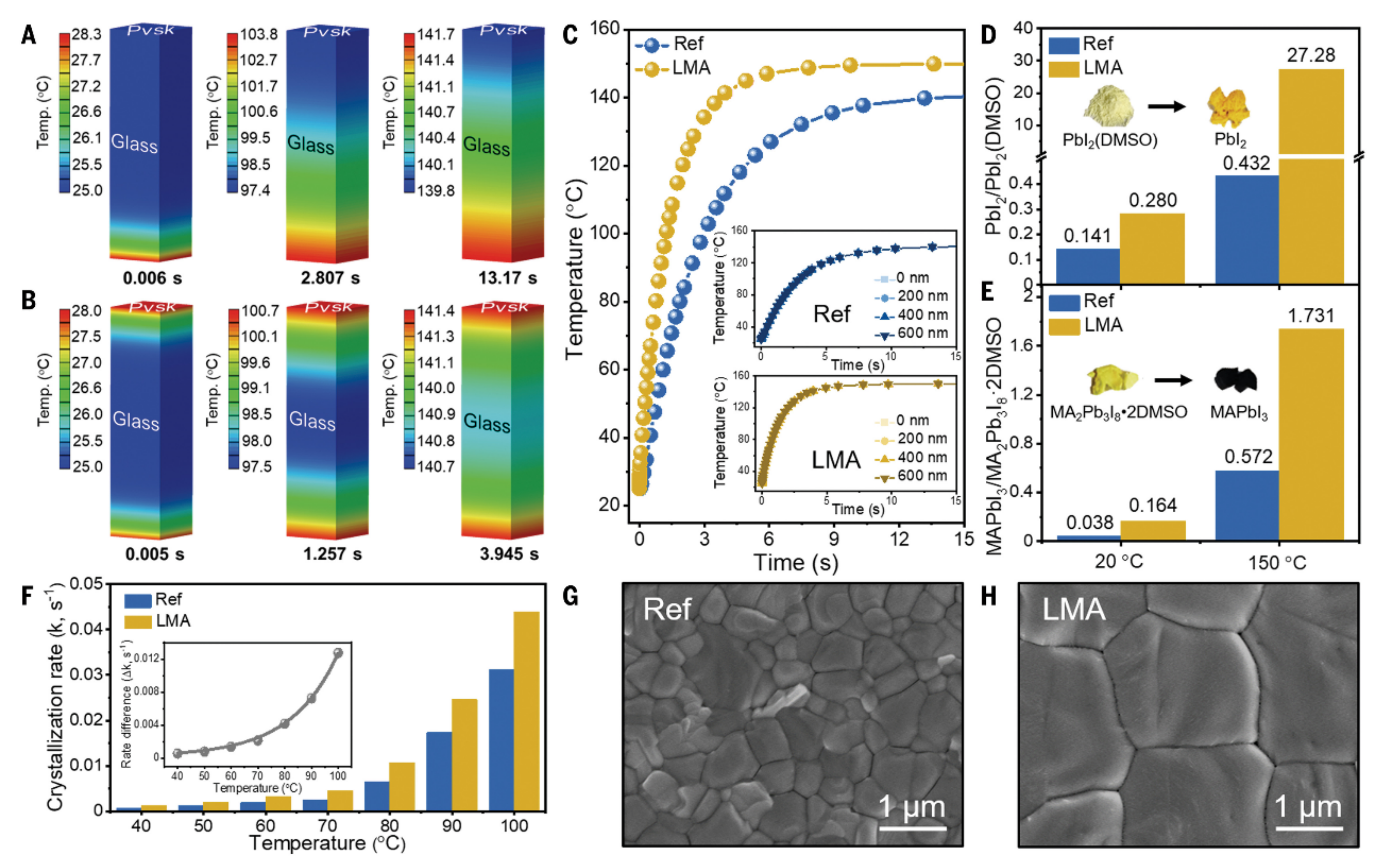
The simulation results showed that the liquid medium annealing (LMA) had a faster heating transfer rate than the hotplate reference (Ref), with the hot anisole providing a temporally homogeneous and stable heat field to drive the high temperature crystallization of perovskite (shown in Figure 15). In addition, the anisole had an excellent ability to extract DMSO, which accelerated the transformation of perovskite and reduced the volatilization of MA+ during the thermal annealing. This method was not affected by the size of the cell’s area or the ambient humidity during the four seasons, and had outstanding reproducibility in film fabrication, which was critical for the future commercial fabrication of PSCs. The environmental humidity would obviously affect the crystallization [167]. The properties of films may be enhanced or compromised by annealing in environments with varying humidity [168]. Therefore, providing a uniform environment to isolation from ambient conditions during annealing process would improve the reproducibility of high-quality films. Ethyl acetate (EA) was also a suitable reagent for the complete removal of polar solvents [165]. The peak positions at 1644, 1310 and 1020 cm− 1 for the unannealed films confirmed the presence of residual DMSO, compared to only one very weak peak at 1018 cm− 1 for the unannealed ethyl acetate-calcite films, indicating that EA could completely remove residual DMSO solvent during the extraction process. Chloroform and IPA washing all had the ability to extract DMSO from lead iodide and accelerate the conversion of lead iodide to dry crystals [128,163].
4.2.3. Encapsulation Layer Annealing
The encapsulation layer annealing was performed by adding a layer on the surface of perovskite to form a sandwich structure with the upper and lower layers [129,169]. The existence of the encapsulated layer in the annealing process improved the film growth by retarding the evaporation of the solvent. The restrained solvent would induce the obvious dissolution–recrystallization process, which led to high quality films with large sized grains. Wei et al. introduced PC61BM as a barrier layer before annealing, which developed a sandwich structure of substrate/perovskite/PC61BM to retard the extravasation of solvent during annealing [169]. The escape of the residual solvent was prevented by the PC61BM, resulting in the dissolution of the grains. The recrystallized grains were coarsened, which improved the photovoltaic performance of PSCs.
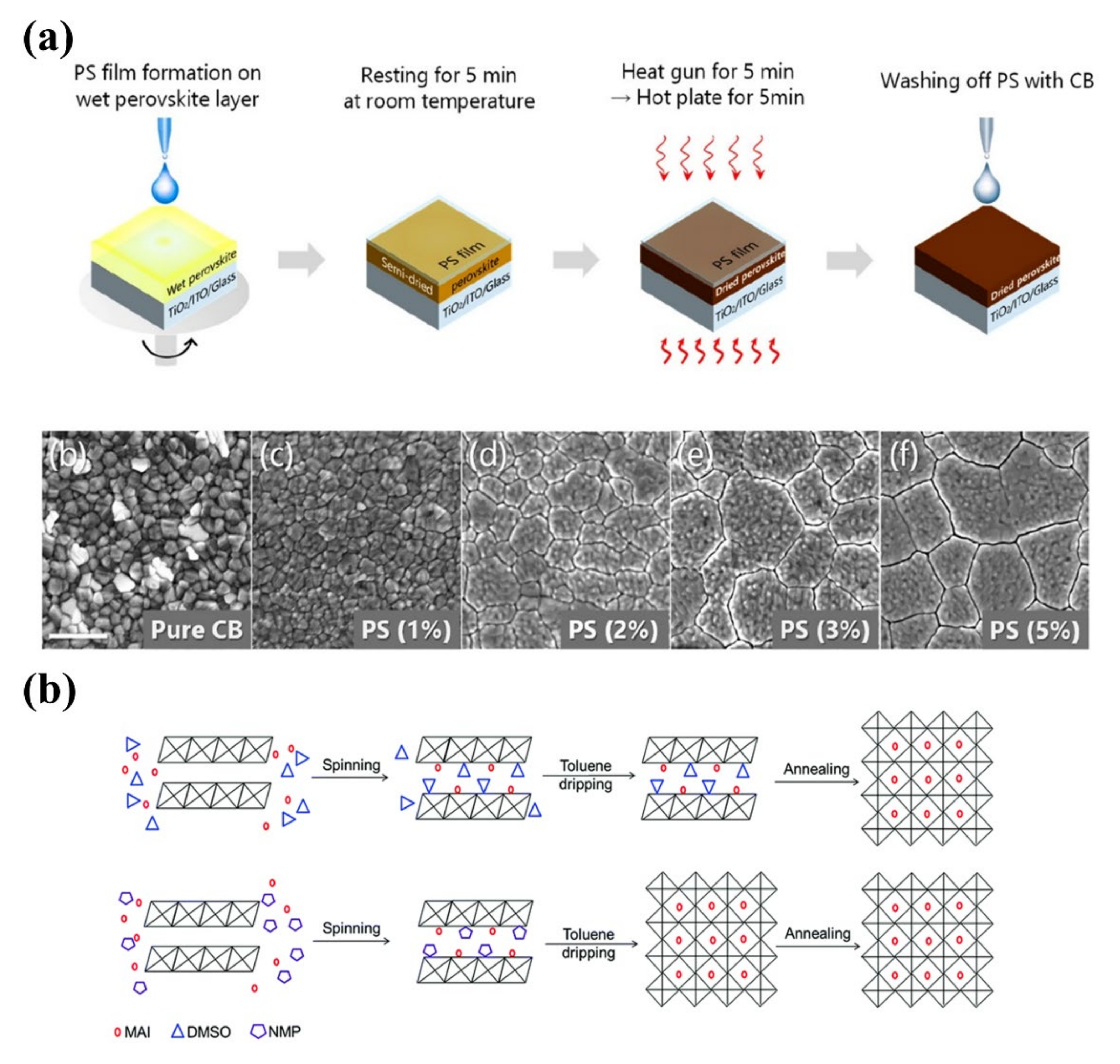
Taylor et al. chose polystyrene (PS) as the encapsulation layer during the annealing process [129]. PS was spin-coated directly onto the wet substrate and washed off by CB after annealing (Figure 16a). The SEM results showed that the growth of the films can be controlled by varying the concentration of PS. The aggregation of grains was more obvious at concentrations above 2%, and larger grain sizes were obtained at higher concentrations. The encapsulation layer would suppress the appearance of δ-phase perovskite, while increasing the grain size of α-phase perovskite. However, this annealing method required the introduction of a layer with the specified thickness, which may not be required in the device structure. The effect of the residual film layer on the PCE and stability of the device was not negligible, and a study of the grain growth on the surface which is in contact with the encapsulation layer during the annealing process is still needed. A possible effect could be detrimental carrier transport between the perovskite layer and the transport layer.
4.2.4. No Annealing
The addition of specific reagents to the precursor solution enables the film to be directly transformed from liquid to solid during the spin-coating process, avoiding additional annealing treatments [127,170,171,172]. Chen et al. proposed a method for the preparation of annealing-free perovskite films by introducing guanidine iodide (GAI) [171]. The organic molecule guanidine (GA (+)) had a large ionic radius, which could control the crystallization rate of annealing-free films, and the films were characterized by low defect density and a large grain size. NMP was added to the dimethylacetamide (DMAc) precursor solution and would insert into the PbI2 lattice to produce an intermediate phase MAI-PbI2-NMP, which was similar to MAI-PbI2-DMSO (Figure 16b) [170]. The NMP was rapidly removed after dropping the antisolvent, completing the immediate nucleation and grain growth of the perovskite film. In addition, 2-Methoxyethanol (2-ME) and NH4Cl also displayed the ability to promote crystallization [127,172]. This crystallization mode had implications for the production of flexible cells, which eliminated pinholes and cracks generated by the thermal annealing process, while improving the reproducibility of the crystallization quality.
5. Conclusions
This paper provides a comprehensive and detailed review of the role of annealing in perovskite films. We classify the current annealing methods into physical and chemical annealing, and systematically investigate the effects and mechanisms of film growth under various annealing modes. Physical annealing includes thermal annealing, electromagnetic wave annealing, ultrasonic annealing and pressure annealing. Among the physical annealing methods, gradient thermal annealing and pressure annealing are the most effective in improving the crystalline quality of thin films, but they are detrimental to the production of flexible cells due to the high temperature and long amount of time required. Electromagnetic annealing shows prominent advantages in reducing crystallization time, for example, intense pulsed flashes achieve crystallization of perovskite within 1 ms, which is competitive for rapid commercial fabrication. On the other hand, the improvement of the crystalline quality of the films is not significant, and sometimes part of the crystalline quality is sacrificed in order to reduce the annealing time. Ultrasonic annealing is a cold working method that is attractive for the production of flexible batteries, and this annealing method can easily be combined with other production equipment. In general, in physical annealing, researchers pay more attention to the combination of annealing methods and industrial production of PSCs; we believe annealing methods with high crystalline quality and ultra-fast crystallization times will be the focus of future research in physical annealing.
Chemical annealing includes solvent annealing, extraction annealing, encapsulation layer annealing and no annealing. Solvent annealing has greater potential for efficiency improvements in devices, and films annealed by recrystallization have excellent grain quality improvements. Although there are various solvents used in solvent annealing, we believe that solvent annealing using substances already present in the film preparation is the better option, allowing for easier removal and reducing the possibility of introducing impurities. Extractive annealing offers excellent reproducibility in film preparation, which provides a uniform preparation environment to isolation from ambient conditions and extraction of residual solvents. Encapsulation layers require the introduction of materials that are not part of the perovskite preparation during the annealing process. However, due to the fragility of perovskite structure, the residual elements may have a negative impact on the stability of the device. No annealing is an important reference value in the production of large area flexible cells, but there is also the need to introduce new ions inside the perovskite.
In summary, in order to improve the growth quality of thin films during the annealing process in the laboratory, we believe that more attention should be attached to the nucleation control of perovskite and the reduction of crystallization rates. The combination of two methods exhibits more outstanding growth quality than the single-method treatment.
With the advance of commercial PSCs applications, we think that future exploration of new annealing methods will focus on three points: higher quality films, extremely fast processing times, and lower costs. Therefore, a single annealing method will not be able to fulfil all the needs, and we suggest that the combined application of various annealing methods may provide a more suitable new approach in the future manufacture of PSCs.
Author Contributions
Conceptualization, L.W.; investigation, X.X., G.Y. and H.Z.; writing—original draft preparation, L.W., G.L., G.Y., B.Z., Y.H., Y.L., H.Q. and S.Z.; writing—review and editing, L.H.; visualization, S.Z.; supervision, H.Z.; project administration, X.X.; funding acquisition, G.L.; All authors have read and agreed to the published version of the manuscript.
Funding
This research was supported by the “National Natural Science Foundation of China (61804066)”, the “China Postdoctoral Science Foundation (2020M671602)” and the “Jiangsu Postdoctoral Science Foundation (2020K143B)”. We acknowledge the funding from the Zhejiang Provincial Innovation Team (2019R01012).
Conflicts of Interest
The authors declare no conflict of interest.
References
- Al-Ashouri, A.; Kohnen, E.; Li, B.; Magomedov, A.; Hempel, H.; Caprioglio, P.; Marquez, J.A.; Vilches, A.B.M.; Kasparavicius, E.; Smith, J.A.; et al. Monolithic perovskite/silicon tandem solar cell with >29% efficiency by enhanced hole extraction. Science 2020, 370, 1300–1309. [Google Scholar] [CrossRef] [PubMed]
- Lee, M.M.; Teuscher, J.; Miyasaka, T.; Murakami, T.N.; Snaith, H.J. Efficient Hybrid Solar Cells Based on Meso-Superstructured Organometal Halide Perovskites. Science 2012, 338, 643–647. [Google Scholar] [CrossRef] [PubMed] [Green Version]
- Saliba, M.; Matsui, T.; Seo, J.Y.; Domanski, K.; Correa-Baena, J.P.; Nazeeruddin, M.K.; Zakeeruddin, S.M.; Tress, W.; Abate, A.; Hagfeldt, A.; et al. Cesium-containing triple cation perovskite solar cells: Improved stability, reproducibility and high efficiency. Energy Environ. Sci. 2016, 9, 1989–1997. [Google Scholar] [CrossRef] [PubMed] [Green Version]
- Zhou, T.W.; Wang, M.; Zang, Z.G.; Tang, X.S.; Fang, L. Two-dimensional lead-free hybrid halide perovskite using superatom anions with tunable electronic properties. Sol. Energy Mater. Sol. Cells 2019, 191, 33–38. [Google Scholar] [CrossRef]
- Kojima, A.; Teshima, K.; Shirai, Y.; Miyasaka, T. Organometal Halide Perovskites as Visible-Light Sensitizers for Photovoltaic Cells. J. Am. Chem. Soc. 2009, 131, 6050–6051. [Google Scholar] [CrossRef]
- Lin, R.X.; Xu, J.; Wei, M.Y.; Wang, Y.R.; Qin, Z.Y.; Liu, Z.; Wu, J.L.; Xiao, K.; Chen, B.; Park, S.M.; et al. All-perovskite tandem solar cells with improved grain surface passivation. Nature 2022, 603, 73–78. [Google Scholar] [CrossRef]
- Xie, F.X.; Zhang, D.; Su, H.M.; Ren, X.G.; Wong, K.S.; Gratzel, M.; Choy, W.C.H. Vacuum-Assisted Thermal Annealing of CH3NH3PbI3 for Highly Stable and Efficient Perovskite Solar Cells. ACS Nano 2015, 9, 639–646. [Google Scholar] [CrossRef]
- Smith, I.C.; Hoke, E.T.; Solis-Ibarra, D.; McGehee, M.D.; Karunadasa, H.I. A Layered Hybrid Perovskite Solar-Cell Absorber with Enhanced Moisture Stability. Angew. Chem. Int. Ed. 2014, 53, 11232–11235. [Google Scholar] [CrossRef]
- Kasperovich, G.; Hausmann, J. Improvement of fatigue resistance and ductility of TiAl6V4 processed by selective laser melting. J. Mater. Processing Technol. 2015, 220, 202–214. [Google Scholar] [CrossRef]
- Chu, J.P.; Jang, J.S.C.; Huang, J.C.; Chou, H.S.; Yang, Y.; Ye, J.C.; Wang, Y.C.; Lee, J.W.; Liu, F.X.; Liaw, P.K.; et al. Thin film metallic glasses: Unique properties and potential applications. Thin Solid Film. 2012, 520, 5097–5122. [Google Scholar] [CrossRef]
- Wang, L.; Huang, M.Q.; Yu, X.F.; You, W.B.; Zhang, J.; Liu, X.H.; Wang, M.; Che, R.C. MOF-Derived Ni1-xCox@Carbon with Tunable Nano-Microstructure as Lightweight and Highly Efficient Electromagnetic Wave Absorber. Nano-Micro Lett. 2020, 12, 150–157. [Google Scholar] [CrossRef]
- Young, C.; Wang, J.; Kim, J.; Sugahara, Y.; Henzie, J.; Yamauchi, Y. Controlled Chemical Vapor Deposition for Synthesis of Nanowire Arrays of Metal-Organic Frameworks and Their Thermal Conversion to Carbon/Metal Oxide Hybrid Materials. Chem. Mater. 2018, 30, 3379–3386. [Google Scholar] [CrossRef]
- Duerinckx, F.; Szlufcik, J. Defect passivation of industrial multicrystalline solar cells based on PECVD silicon nitride. Sol. Energy Mater. Sol. Cells 2002, 72, 231–246. [Google Scholar] [CrossRef]
- Kim, J.M.; Kim, Y.K. Thin crystalline silicon solar cell bonded to sintered substrate with aluminum paste. Sol. Energy Mater. Sol. Cells 2005, 86, 577–584. [Google Scholar] [CrossRef]
- Li, D.; de Moraes, E.G.; Guo, P.; Zou, J.; Zhang, J.Z.; Colombo, P.; Shen, Z.J. Rapid sintering of silicon nitride foams decorated with one-dimensional nanostructures by intense thermal radiation. Sci. Technol. Adv. Mater. 2014, 15, 045003–045010. [Google Scholar] [CrossRef] [Green Version]
- Wu, W. Inorganic nanomaterials for printed electronics: A review. Nanoscale 2017, 9, 7342–7372. [Google Scholar] [CrossRef]
- Qin, J.; Zhang, W.J.; Bai, S.X.; Liu, Z.F. Study on the sintering and contact formation process of silver front side metallization pastes for crystalline silicon solar cells. Appl. Surf. Sci. 2016, 376, 52–61. [Google Scholar] [CrossRef]
- Cao, X.B.; Zhi, L.L.; Jia, Y.; Li, Y.H.; Cui, X.; Zhao, K.; Ci, L.J.; Ding, K.X.; Wei, J.Q. High annealing temperature induced rapid grain coarsening for efficient perovskite solar cells. J. Colloid Interface Sci. 2018, 524, 483–489. [Google Scholar] [CrossRef]
- Dualeh, A.; Tetreault, N.; Moehl, T.; Gao, P.; Nazeeruddin, M.K.; Gratzel, M. Effect of Annealing Temperature on Film Morphology of Organic-Inorganic Hybrid Pervoskite Solid-State Solar Cells. Adv. Funct. Mater. 2014, 24, 3250–3258. [Google Scholar] [CrossRef]
- Singh, T.; Miyasaka, T. Stabilizing the Efficiency Beyond 20% with a Mixed Cation Perovskite Solar Cell Fabricated in Ambient Air under Controlled Humidity. Adv. Energy Mater. 2018, 8, 1700677. [Google Scholar] [CrossRef]
- Xiao, Z.G.; Dong, Q.F.; Bi, C.; Shao, Y.C.; Yuan, Y.B.; Huang, J.S. Solvent Annealing of Perovskite-Induced Crystal Growth for Photovoltaic-Device Efficiency Enhancement. Adv. Mater. 2014, 26, 6503–6509. [Google Scholar] [CrossRef]
- Liu, D.B.; Zeng, Q.X.; Yao, Y.Q.; Liang, H.F.; Chen, L.J.; Song, Q.L. Controllable Multistep Preparation Method for High-Efficiency Perovskite Solar Cells with Low Annealing Temperature in Glove Box. Energy Technol. 2020, 8, 2000071. [Google Scholar] [CrossRef]
- You, P.; Li, G.J.; Tang, G.Q.; Cao, J.P.; Yan, F. Ultrafast laser-annealing of perovskite films for efficient perovskite solar cells. Energy Environ. Sci. 2020, 13, 1187–1196. [Google Scholar] [CrossRef]
- Bruening, K.; Tassone, C.J. Antisolvent processing of lead halide perovskite thin films studied by in situ X-ray diffraction. J. Mater. Chem. A 2018, 6, 18865–18870. [Google Scholar] [CrossRef]
- Chen, S.S.; Xiao, X.; Chen, B.; Kelly, L.L.; Zhao, J.J.; Lin, Y.Z.; Toney, M.F.; Huang, J.S. Crystallization in one-step solution deposition of perovskite films: Upward or downward? Sci. Adv. 2021, 7, eabb2412. [Google Scholar] [CrossRef]
- Mahmud, M.A.; Elumalai, N.K.; Upama, M.B.; Wang, D.; Haque, F.; Wright, M.; Xu, C.; Uddin, A. Controlled nucleation assisted restricted volume solvent annealing for stable perovskite solar cells. Sol. Energy Mater. Sol. Cells 2017, 167, 70–86. [Google Scholar] [CrossRef]
- Shargaieva, O.; Nasstrom, H.; Smith, J.A.; Tobbens, D.; Munir, R.; Unger, E. Hybrid perovskite crystallization from binary solvent mixtures: Interplay of evaporation rate and binding strength of solvents. Mater. Adv. 2020, 1, 3314–3321. [Google Scholar] [CrossRef]
- Barrows, A.T.; Lilliu, S.; Pearson, A.J.; Babonneau, D.; Dunbar, A.D.F.; Lidzey, D.G. Monitoring the Formation of a CH3NH3PbI3-xClx Perovskite during Thermal Annealing Using X-Ray Scattering. Adv. Funct. Mater. 2016, 26, 4934–4942. [Google Scholar] [CrossRef] [Green Version]
- Suchan, K.; Just, J.; Becker, P.; Unger, E.L.; Unold, T. Optical in situ monitoring during the synthesis of halide perovskite solar cells reveals formation kinetics and evolution of optoelectronic properties. J. Mater. Chem. A 2020, 8, 10439–10449. [Google Scholar] [CrossRef]
- Serpetzoglou, E.; Konidakis, I.; Maksudov, T.; Panagiotopoulos, A.; Kymakis, E.; Stratakis, E. In situ monitoring of the charge carrier dynamics of CH3NH3PbI3 perovskite crystallization process. J. Mater. Chem. C 2019, 7, 12170–12179. [Google Scholar] [CrossRef]
- Frost, J.M.; Butler, K.T.; Brivio, F.; Hendon, C.H.; van Schilfgaarde, M.; Walsh, A. Atomistic Origins of High-Performance in Hybrid Halide Perovskite Solar Cells. Nano Lett. 2014, 14, 2584–2590. [Google Scholar] [CrossRef] [PubMed] [Green Version]
- Shi, S.W.; Li, Y.F.; Li, X.Y.; Wang, H.Q. Advancements in all-solid-state hybrid solar cells based on organometal halide perovskites. Mater. Horiz. 2015, 2, 378–405. [Google Scholar] [CrossRef]
- Seo, J.Y.; Matsui, T.; Luo, J.S.; Correa-Baena, J.P.; Giordano, F.; Saliba, M.; Schenk, K.; Ummadisingu, A.; Domanski, K.; Hadadian, M.; et al. Ionic Liquid Control Crystal Growth to Enhance Planar Perovskite Solar Cells Efficiency. Adv. Energy Mater. 2016, 6, 1600767. [Google Scholar] [CrossRef]
- Wang, M.H.; Wang, W.; Ma, B.; Shen, W.; Liu, L.H.; Cao, K.; Chen, S.F.; Huang, W. Lead-Free Perovskite Materials for Solar Cells. Nano-Micro Lett. 2021, 13, 21. [Google Scholar] [CrossRef]
- Chen, P.; Bai, Y.; Wang, S.C.; Lyu, M.Q.; Yun, J.H.; Wang, L.Z. In Situ Growth of 2D Perovskite Capping Layer for Stable and Efficient Perovskite Solar Cells. Adv. Funct. Mater. 2018, 28, 1706923. [Google Scholar] [CrossRef]
- Hou, Y.; Aydin, E.; De Bastiani, M.; Xiao, C.X.; Isikgor, F.H.; Xue, D.J.; Chen, B.; Chen, H.; Bahrami, B.; Chowdhury, A.H.; et al. Efficient tandem solar cells with solution-processed perovskite on textured crystalline silicon. Science 2020, 367, 1135–1140. [Google Scholar] [CrossRef]
- Moore, D.T.; Sai, H.; Tan, K.W.; Estroff, L.A.; Wiesner, U. Impact of the organic halide salt on final perovskite composition for photovoltaic applications. APL Mater. 2014, 2, 081802. [Google Scholar] [CrossRef] [Green Version]
- Guo, X.; McCleese, C.; Kolodziej, C.; Samia, A.C.S.; Zhao, Y.X.; Burda, C. Identification and characterization of the intermediate phase in hybrid organic-inorganic MAPbI(3) perovskite. Dalton Trans. 2016, 45, 3806–3813. [Google Scholar] [CrossRef]
- Liu, Y.H.; Akin, S.; Hinderhofer, A.; Eickemeyer, F.T.; Zhu, H.W.; Seo, J.Y.; Zhang, J.H.; Schreiber, F.; Zhang, H.; Zakeeruddin, S.M.; et al. Stabilization of Highly Efficient and Stable Phase-Pure FAPbI(3)Perovskite Solar Cells by Molecularly Tailored 2D-Overlayers. Angew. Chem. Int. Ed. 2020, 59, 15688–15694. [Google Scholar] [CrossRef]
- Zhang, Y.; Seo, S.; Lim, S.Y.; Kim, Y.; Kim, S.G.; Lee, D.K.; Lee, S.H.; Shin, H.; Cheong, H.; Park, N.G. Achieving Reproducible and High-Efficiency (>21%) Perovskite Solar Cells with a Presynthesized FAPbI(3) Powder. Acs Energy Lett. 2020, 5, 360–366. [Google Scholar] [CrossRef]
- Frolova, L.A.; Anokhin, D.V.; Piryazev, A.A.; Luchkin, S.Y.; Dremova, N.N.; Stevenson, K.J.; Troshin, P.A. Highly Efficient All-Inorganic Planar Heterojunction Perovskite Solar Cells Produced by Thermal Coevaporation of CsI and PbI2. J. Phys. Chem. Lett. 2017, 8, 67–72. [Google Scholar] [CrossRef]
- Ahmad, W.; Khan, J.; Niu, G.D.; Tang, J. Inorganic CsPbI3 Perovskite-Based Solar Cells: A Choice for a Tandem Device. Sol. Rrl 2017, 1, 1700048. [Google Scholar] [CrossRef]
- Liu, C.; Yang, Y.; Xia, X.; Ding, Y.; Arain, Z.; An, S.J.; Liu, X.P.; Cristina, R.C.; Dai, S.Y.; Nazeeruddin, M.K. Soft Template-Controlled Growth of High-Quality CsPbI3 Films for Efficient and Stable Solar Cells. Adv. Energy Mater. 2020, 10, 1903751. [Google Scholar] [CrossRef]
- Dinegar, V.K.L.R.H. Theory, Production and Mechanism of Formation of Monodispersed Hydrosols. J. Am. Chem. Soc 1950, 72, 4847–4854. [Google Scholar] [CrossRef]
- Sun, Y.G. Controlled synthesis of colloidal silver nanoparticles in organic solutions: Empirical rules for nucleation engineering. Chem. Soc. Rev. 2013, 42, 2497–2511. [Google Scholar] [CrossRef]
- Dunlap-Shohl, W.A.; Zhou, Y.; Padture, N.P.; Mitzi, D.B. Synthetic Approaches for Halide Perovskite Thin Films. Chem. Rev. 2019, 119, 3193–3295. [Google Scholar] [CrossRef]
- Chen, J.W.; Hillig, W.B.; Sears, G.W. The molecular mechanism of solidifition. Acta Metall. 1964, 12, 1421–1439. [Google Scholar] [CrossRef]
- Cahn, J.W. Theory of crystal growth and interface motion. Acta Metall. 1960, 8, 554–562. [Google Scholar] [CrossRef]
- Jie, W. Principle and Technology of Crystal Growth; Science Press: Beijing, China, 2009. [Google Scholar]
- Donnay, J.D.H.; Harker, D. A new law of crystal morphology extending the Law of Bravais. Am. Mineral. 1937, 22, 446–467. [Google Scholar]
- Hua, J.C.; Deng, X.; Niu, C.; Huang, F.Z.; Peng, Y.; Li, W.N.; Ku, Z.L.; Cheng, Y.B. A pressure-assisted annealing method for high quality CsPbBr3 film deposited by sequential thermal evaporation. RSC Adv. 2020, 10, 8905–8909. [Google Scholar] [CrossRef] [Green Version]
- Ghahremani, A.H.; Ratnayake, D.; Sherehiy, A.; Popa, D.O.; Druffel, T. Automated Fabrication of Perovskite Photovoltaics Using Inkjet Printing and Intense Pulse Light Annealing. Energy Technol. 2021, 9, 2100452. [Google Scholar] [CrossRef]
- Bi, C.; Shao, Y.C.; Yuan, Y.B.; Xiao, Z.G.; Wang, C.G.; Gao, Y.L.; Huang, J.S. Understanding the formation and evolution of interdiffusion grown organolead halide perovskite thin films by thermal annealing. J. Mater. Chem. A 2014, 2, 18508–18514. [Google Scholar] [CrossRef]
- Liu, C.; Cheng, Y.B.; Ge, Z.Y. Understanding of perovskite crystal growth and film formation in scalable deposition processes. Chem. Soc. Rev. 2020, 49, 1653–1687. [Google Scholar] [CrossRef] [PubMed]
- Wang, S.B.; Chen, Y.Q.; Li, R.Y.; Xu, Y.B.; Feng, J.S.; Yang, D.; Yuan, N.Y.; Zhang, W.H.; Liu, S.; Ding, J.N. Superior Textured Film and Process Tolerance Enabled by Intermediate-State Engineering for High-Efficiency Perovskite Solar Cells. Adv. Sci. 2020, 7, 1903009. [Google Scholar] [CrossRef] [Green Version]
- Qin, M.C.; Tse, K.F.; Lau, T.K.; Li, Y.H.; Su, C.J.; Yang, G.; Chen, J.H.; Zhu, J.Y.; Jeng, U.S.; Li, G.; et al. Manipulating the Mixed-Perovskite Crystallization Pathway Unveiled by In Situ GIWAXS. Adv. Mater. 2019, 31, 1901284. [Google Scholar] [CrossRef]
- Kim, G.; Moon, C.S.; Yang, T.-Y.; Kim, Y.Y.; Chung, J.; Jung, E.H.; Shin, T.J.; Jeon, N.J.; Park, H.H.; Seo, J. A Thermally Induced Perovskite Crystal Control Strategy for Efficient and Photostable Wide-Bandgap Perovskite Solar Cells. Sol. RRL 2020, 4, 2000033. [Google Scholar] [CrossRef]
- Van Franeker, J.J.; Hendriks, K.H.; Bruijnaers, B.J.; Verhoeven, M.; Wienk, M.M.; Janssen, R.A.J. Monitoring Thermal Annealing of Perovskite Solar Cells with In Situ Photoluminescence. Adv. Energy Mater. 2017, 7, 1601822. [Google Scholar] [CrossRef] [Green Version]
- Kim, M.; Kim, G.H.; Oh, K.S.; Jo, Y.; Yoon, H.; Kim, K.H.; Lee, H.; Kim, J.Y.; Kim, D.S. High-Temperature-Short-Time Annealing Process for High-Performance Large-Area Perovskite Solar Cells. Acs Nano 2017, 11, 6057–6064. [Google Scholar] [CrossRef]
- Shargaieva, O.; Lang, F.; Rappich, J.; Dittrich, T.; Kalus, M.; Meixner, M.; Genzel, C.; Nickel, N.H. Influence of the Grain Size on the Properties of CH3NH3PbI3 Thin Films. Acs Appl. Mater. Interfaces 2017, 9, 38428–38435. [Google Scholar] [CrossRef]
- Lin, P.A.; Zhang, W.F.; Tian, L.W.; Zhang, F.; Zhou, S.H.; Liu, R.; Hu, T.T.; Zhang, M.; Du, L.; Wen, F.; et al. Remanent solvent management engineering of perovskite films for PEDOT: PSS-based inverted solar cells. Sol. Energy 2021, 216, 530–536. [Google Scholar] [CrossRef]
- Huang, L.K.; Hu, Z.Y.; Xu, J.; Zhang, K.; Zhang, J.; Zhu, Y.J. Multi-step slow annealing perovskite films for high performance planar perovskite solar cells. Sol. Energy Mater. Sol. Cells 2015, 141, 377–382. [Google Scholar] [CrossRef]
- Zhang, J.; Liang, W.S.; Yu, W.; Yu, S.W.; Wu, Y.L.; Guo, X.; Liu, S.Z.; Li, C. A Two-Stage Annealing Strategy for Crystallization Control of CH3NH3PbI3 Films toward Highly Reproducible Perovskite Solar Cells. Small 2018, 14, 1800181. [Google Scholar] [CrossRef]
- Fan, B.B.; Peng, D.H.; Lin, S.W.; Wang, N.; Zhao, Y.; Sun, Y.M. Enhanced efficiency of planar-heterojunction perovskite solar cells through a thermal gradient annealing process. Rsc Adv. 2015, 5, 58041–58045. [Google Scholar] [CrossRef]
- Xi, J.H.; Yuan, J.F.; Yan, X.Q.; Binks, D.; Tian, J.J. Gradient Annealing of Halide Perovskite Films for Improved Performance of Solar Cells. Acs Appl. Energy Mater. 2020, 3, 8130–8134. [Google Scholar] [CrossRef]
- Xiao, Y.Y.; Meng, Y.Q.; Gao, H.L.; Chen, Y.C.; Meng, Q.; Bai, Y.J.; Wang, H.; Zhang, Y.Z.; Yan, H.; Han, C.B. Flexible perovskite solar cells fabricated by a gradient heat treatment process. Sustain. Energy Fuels 2020, 4, 824–831. [Google Scholar] [CrossRef]
- Chen, W.J.; Chen, H.Y.; Xu, G.Y.; Xue, R.M.; Wang, S.H.; Li, Y.W.; Li, Y.F. Precise Control of Crystal Growth for Highly Efficient CsPbI2Br Perovskite Solar Cells. Joule 2019, 3, 191–204. [Google Scholar] [CrossRef] [Green Version]
- Song, Q.; Liang, C.J.; Zhang, H.M.; Ji, C.; Sun, M.J.; Sun, F.L.; Jing, X.P.; You, F.T.; Lu, Y.W.; He, Z.Q. Additional Organic-Solvent-Rinsing Process to Enhance Perovskite Photovoltaic Performance. Adv. Electron. Mater. 2019, 5, 1900244. [Google Scholar] [CrossRef]
- Sadeghi, A.; Hassanzadeh, H.; Harding, T.G. Thermal analysis of high frequency electromagnetic heating of lossy porous media. Chem. Eng. Sci. 2017, 172, 13–22. [Google Scholar] [CrossRef]
- Ankireddy, K.; Ghahremani, A.H.; Martin, B.; Gupta, G.; Druffel, T. Rapid thermal annealing of CH3NH3PbI3 perovskite thin films by intense pulsed light with aid of diiodomethane additive. J. Mater. Chem. A 2018, 6, 9378–9383. [Google Scholar] [CrossRef]
- Nam, J.B.; Jang, Y.R.; Hwang, Y.T.; Kim, H.H.; Jung, I.H.; Kim, H.S. Intense Pulsed Light Sintering of Screen-Printed Paste Electrode on Silicon Solar Cell for High Throughput and Cost-Effective Low Temperature Metallization. Int. J. Precis. Eng. Manuf. -Green Technol. 2022, 9, 523–535. [Google Scholar] [CrossRef]
- Sharma, B.; Singh, S.; Pareek, S.; Agasti, A.; Mallick, S.; Kabra, D.; Bhargava, P. Radiative and conductive thermal annealing of hybrid organic-inorganic perovskite layer. Sol. Energy Mater. Sol. Cells 2019, 195, 353–357. [Google Scholar] [CrossRef]
- Girolami, M.; Bellucci, A.; Mastellone, M.; Serpente, V.; Orlando, S.; Valentini, V.; Palma, A.L.; Di Carlo, A.; Trucchi, D.M. Improving the Performance of Printable Carbon Electrodes by Femtosecond Laser Treatment. C-J. Carbon Res. 2020, 6, 48. [Google Scholar] [CrossRef]
- Druffel, T.; Dharmadasa, R.; Lavery, B.W.; Ankireddy, K. Intense pulsed light processing for photovoltaic manufacturing. Sol. Energy Mater. Sol. Cells 2018, 174, 359–369. [Google Scholar] [CrossRef]
- Ghahremani, A.H.; Pishgar, S.; Bahadur, J.; Druffel, T. Intense Pulse Light Annealing of Perovskite Photovoltaics Using Gradient Flashes. Acs Appl. Energy Mater. 2020, 3, 11641–11654. [Google Scholar] [CrossRef]
- Lavery, B.W.; Kumari, S.; Konermann, H.; Draper, G.L.; Spurgeon, J.; Druffel, T. Intense Pulsed Light Sintering of CH3NH3PbI3 Solar Cells. Acs Appl. Mater. Interfaces 2016, 8, 8419–8426. [Google Scholar] [CrossRef]
- Piper, R.T.; Daunis, T.B.; Xu, W.J.; Schroder, K.A.; Hsu, J.W.P. Photonic Curing of Nickel Oxide Transport Layer and Perovskite Active Layer for Flexible Perovskite Solar Cells: A Path Towards High-Throughput Manufacturing. Front. Energy Res. 2021, 9, 640960. [Google Scholar] [CrossRef]
- Xu, W.J.; Daunis, T.B.; Piper, R.T.; Hsu, J.W.P. Effects of Photonic Curing Processing Conditions on MAPbI(3) Film Properties and Solar Cell Performance. Acs Appl. Energy Mater. 2020, 3, 8636–8645. [Google Scholar] [CrossRef]
- Bahadur, J.; Ghahremani, A.H.; Gupta, S.; Druffel, T.; Sunkara, M.K.; Pal, K. Enhanced moisture stability of MAPbI(3) perovskite solar cells through Barium doping. Sol. Energy 2019, 190, 396–404. [Google Scholar] [CrossRef]
- Muydinov, R.; Seeger, S.; Kumar, S.; Klimm, C.; Kraehnert, R.; Wagner, M.R.; Szyszka, B. Crystallisation behaviour of CH3NH3PbI3 films: The benefits of sub-second flash lamp annealing. Thin Solid Film. 2018, 653, 204–214. [Google Scholar] [CrossRef]
- Troughton, J.; Carnie, M.J.; Davies, M.L.; Charbonneau, C.; Jewell, E.H.; Worsley, D.A.; Watson, T.M. Photonic flash-annealing of lead halide perovskite solar cells in 1 ms. J. Mater. Chem. A 2016, 4, 3471–3476. [Google Scholar] [CrossRef]
- Sanchez, S.; Christoph, N.; Grobety, B.; Phung, N.; Steiner, U.; Saliba, M.; Abate, A. Efficient and Stable Inorganic Perovskite Solar Cells Manufactured by Pulsed Flash Infrared Annealing. Adv. Energy Mater. 2018, 8, 1802060. [Google Scholar] [CrossRef] [Green Version]
- Feleki, B.; Bex, G.; Andriessen, R.; Galagan, Y.; Di Giacomo, F. Rapid and low temperature processing of mesoporous TiO2 for perovskite solar cells on flexible and rigid substrates. Mater. Today Commun. 2017, 13, 232–240. [Google Scholar] [CrossRef] [Green Version]
- Wang, L.; Liu, G.L.; Xi, X.; Zhu, B.J.; Li, S.M.; Shao, J.B.; Zhu, F.; Feng, H.Y. Infrared photon-assisted annealing for crystal engineering in perovskite solar cells. Bull. Mater. Sci. 2022, 45, 54. [Google Scholar] [CrossRef]
- Gunzler, A.; Bermudez-Urena, E.; Muscarella, L.A.; Ochoa, M.; Ochoa-Martinez, E.; Ehrler, B.; Saliba, M.; Steiner, U. Shaping Perovskites: In Situ Crystallization Mechanism of Rapid Thermally Annealed, Prepatterned Perovskite Films. ACS Appl Mater Interfaces 2021, 13, 6854–6863. [Google Scholar] [CrossRef]
- Huang, S.H.; Guan, C.K.; Lee, P.H.; Huang, H.C.; Li, C.F.; Huang, Y.C.; Su, W.F. Toward All Slot-Die Fabricated High Efficiency Large Area Perovskite Solar Cell Using Rapid Near Infrared Heating in Ambient Air. Adv. Energy Mater. 2020, 10, 2001567. [Google Scholar] [CrossRef]
- Sánchez, S.; Vallés-Pelarda, M.; Alberola-Borràs, J.-A.; Vidal, R.; Jerónimo-Rendón, J.J.; Saliba, M.; Boix, P.P.; Mora-Seró, I. Flash infrared annealing as a cost-effective and low environmental impact processing method for planar perovskite solar cells. Mater. Today 2019, 31, 39–46. [Google Scholar] [CrossRef]
- Ling, P.S.V.; Hagfeldt, A.; Sanchez, S. Flash Infrared Annealing for Perovskite Solar Cell Processing. J. Vis. Exp. 2021, 168, e61730. [Google Scholar] [CrossRef]
- Sanchez, S.; Hua, X.; Phung, N.; Steiner, U.; Abate, A. Flash Infrared Annealing for Antisolvent-Free Highly Efficient Perovskite Solar Cells. Adv. Energy Mater. 2018, 8, 1702915. [Google Scholar] [CrossRef]
- Troughton, J.; Charbonneau, C.; Carnie, M.J.; Davies, M.L.; Worsley, D.A.; Watson, T.M. Rapid processing of perovskite solar cells in under 2.5 s. J. Mater. Chem. A 2015, 3, 9123–9127. [Google Scholar] [CrossRef]
- Qiu, Z.W.; Gong, H.B.; Zheng, G.H.J.; Yuan, S.A.; Zhang, H.L.; Zhu, X.M.; Zhou, H.P.; Cao, B.Q. Enhanced physical properties of pulsed laser deposited NiO films via annealing and lithium doping for improving perovskite solar cell efficiency. J. Mater. Chem. C 2017, 5, 7084–7094. [Google Scholar] [CrossRef]
- Wilkes, G.C.; Deng, X.Y.; Choi, J.J.; Gupta, M.C. Laser Annealing of TiO2 Electron-Transporting Layer in Perovskite Solar Cells. Acs Appl. Mater. Interfaces 2018, 10, 41312–41317. [Google Scholar] [CrossRef]
- Xia, R.; Yin, G.Y.; Wang, S.M.; Dong, W.W.; You, L.B.; Meng, G.; Fang, X.D.; Nazeeruddin, M.K.; Fei, Z.F.; Dyson, P.J. Precision excimer laser annealed Ga-doped ZnO electron transport layers for perovskite solar cells. Rsc Adv. 2018, 8, 17694–17701. [Google Scholar] [CrossRef] [Green Version]
- Jeon, T.; Jin, H.M.; Lee, S.H.; Lee, J.M.; Park, H.I.; Kim, M.K.; Lee, K.J.; Shin, B.; Kim, S.O. Laser Crystallization of Organic-Inorganic Hybrid Perovskite Solar Cells. Acs Nano 2016, 10, 7907–7914. [Google Scholar] [CrossRef]
- Konidakis, I.; Maksudov, T.; Serpetzoglou, E.; Kakavelakis, G.; Kymakis, E.; Stratakis, E. Improved Charge Carrier Dynamics of CH3NH3PbI3 Perovskite Films Synthesized by Means of Laser-Assisted Crystallization. Acs Appl. Energy Mater. 2018, 1, 5101–5111. [Google Scholar] [CrossRef]
- Song, C.P.; Tong, L.; Liu, F.; Ye, L.; Cheng, G.J. Addressing the Reliability and Electron Transport Kinetics in Halide Perovskite Film via Pulsed Laser Engineering. Adv. Funct. Mater. 2020, 30, 1906781. [Google Scholar] [CrossRef]
- Trinh, X.L.; Tran, N.H.; Seo, H.; Kim, H.C. Enhanced performance of perovskite solar cells via laser-induced heat treatment on perovskite film. Sol. Energy 2020, 206, 301–307. [Google Scholar] [CrossRef]
- Yang, H.R.; Song, C.P.; Xia, T.C.; Li, S.F.; Sun, D.Y.; Liu, F.; Cheng, G.J. Ultrafast transformation of PbI2 in two-step fabrication of halide perovskite films for long-term performance and stability via nanosecond laser shock annealing. J. Mater. Chem. C 2021, 9, 12819–12827. [Google Scholar] [CrossRef]
- Li, F.M.; Zhu, W.D.; Bao, C.X.; Yu, T.; Wang, Y.Q.; Zhou, X.X.; Zou, Z.G. Laser-assisted crystallization of CH3NH3PbI3 films for efficient perovskite solar cells with a high open-circuit voltage. Chem. Commun. 2016, 52, 5394–5397. [Google Scholar] [CrossRef]
- Jones, T.W.; Osherov, A.; Alsari, M.; Sponseller, M.; Duck, B.C.; Jung, Y.K.; Settens, C.; Niroui, F.; Brenes, R.; Stan, C.V.; et al. Lattice strain causes non-radiative losses in halide perovskites. Energy Environ. Sci. 2019, 12, 596–606. [Google Scholar] [CrossRef] [Green Version]
- Zhu, C.; Niu, X.X.; Fu, Y.H.; Li, N.X.; Hu, C.; Chen, Y.H.; He, X.; Na, G.R.; Liu, P.F.; Zai, H.C.; et al. Strain engineering in perovskite solar cells and its impacts on carrier dynamics. Nat. Commun. 2019, 10, 815. [Google Scholar] [CrossRef] [Green Version]
- Lee, S.W.; Kim, S.; Bae, S.; Cho, K.; Chung, T.; Mundt, L.E.; Lee, S.; Park, S.; Park, H.; Schubert, M.C.; et al. UV Degradation and Recovery of Perovskite Solar Cells. Sci. Rep. 2016, 6, 38150. [Google Scholar] [CrossRef] [PubMed] [Green Version]
- Wali, Q.; Iftikhar, F.J.; Khan, M.E.; Ullah, A.; Iqbal, Y.; Jose, R. Advances in stability of perovskite solar cells. Org. Electron. 2020, 78, 105590. [Google Scholar] [CrossRef]
- Ouyang, Z.L.; Abrams, H.; Bergstone, R.; Li, Q.T.; Zhu, F.; Li, D.W. Rapid Layer-Specific Annealing Enabled by Ultraviolet LED with Estimation of Crystallization Energy for High-Performance Perovskite Solar Cells. Adv. Energy Mater. 2020, 10, 1902898. [Google Scholar] [CrossRef]
- Sun, J.; Wang, W.L.; Yue, Q.Y. Review on Microwave-Matter Interaction Fundamentals and Efficient Microwave-Associated Heating Strategies. Materials 2016, 9, 231. [Google Scholar] [CrossRef] [Green Version]
- Motshekga, S.C.; Pillai, S.K.; Ray, S.S.; Jalama, K.; Krause, R.W.M. Recent Trends in the Microwave-Assisted Synthesis of Metal Oxide Nanoparticles Supported on Carbon Nanotubes and Their Applications. J. Nanomater. 2012, 2012, 691503. [Google Scholar] [CrossRef] [Green Version]
- Venkatesh, M.S.; Raghavan, G.S.V. An overview of microwave processing and dielectric properties of agri-food materials. Biosyst. Eng. 2004, 88, 1–18. [Google Scholar] [CrossRef]
- Xu, J.; Hu, Z.Y.; Jia, X.Y.; Huang, L.K.; Huang, X.K.; Wang, L.M.; Wang, P.; Zhang, H.C.; Zhang, J.; Zhang, J.J.; et al. A rapid annealing technique for efficient perovskite solar cells fabricated in air condition under high humidity. Org. Electron. 2016, 34, 84–90. [Google Scholar] [CrossRef] [Green Version]
- Chen, Q.; Ma, T.T.; Wang, F.F.; Liu, Y.; Liu, S.Z.; Wang, J.A.; Cheng, Z.C.; Chang, Q.; Yang, R.; Huang, W.C.; et al. Rapid Microwave-Annealing Process of Hybrid Perovskites to Eliminate Miscellaneous Phase for High Performance Photovoltaics. Adv. Sci. 2020, 7, 2000480. [Google Scholar] [CrossRef]
- Brites, M.J.; Barreiros, M.A.; Corregidor, V.; Alves, L.C.; Pinto, J.V.; Mendes, M.J.; Fortunato, E.; Martins, R.; Mascarenhas, J. Ultrafast Low-Temperature Crystallization of Solar Cell Graded Formamidinium-Cesium Mixed-Cation Lead Mixed-Halide Perovskites Using a Reproducible Microwave-Based Process. Acs Appl. Energy Mater. 2019, 2, 1844–1853. [Google Scholar] [CrossRef]
- Maitani, M.M.; Iso, D.; Kim, J.; Tsubaki, S.; Wada, Y. Microwave Application to Efficient Annealing Process of CH3NH3PbI3 Perovskite Crystalline Films. Electrochemistry 2017, 85, 236–240. [Google Scholar] [CrossRef] [Green Version]
- Cao, Q.P.; Yang, S.W.; Gao, Q.Q.; Lei, L.; Yu, Y.; Shao, J.; Liu, Y. Fast and Controllable Crystallization of Perovskite Films by Microwave Irradiation Process. Acs Appl. Mater. Interfaces 2016, 8, 7854–7861. [Google Scholar] [CrossRef]
- Ahmadian-Yazdi, M.R.; Eslamian, M. Toward scale-up of perovskite solar cells: Annealing-free perovskite layer by low-cost ultrasonic substrate vibration of wet films. Mater. Today Commun. 2018, 14, 151–159. [Google Scholar] [CrossRef]
- Zhang, X.; Zabihi, F.; Xiong, H.; Eslamian, M.; Hou, C.Y.; Zhu, M.F.; Wang, H.Z.; Zhang, Q.H. Highly efficient flexible perovskite solar cells made via ultrasonic vibration assisted room temperature cold sintering. Chem. Eng. J. 2020, 394, 124887. [Google Scholar] [CrossRef]
- Takizawa, K.; Fukudome, H.; Kozaki, Y.; Ando, S. Pressure-Induced Changes in Crystalline Structures of Polyimides Analyzed by Wide-Angle X-ray Diffraction at High Pressures. Macromolecules 2014, 47, 3951–3958. [Google Scholar] [CrossRef]
- Tan, X.; Wang, K.; Li, S.; Yuan, H.; Yan, T.; Liu, J.; Yang, K.; Liu, B.; Zou, G.; Zou, B. Exploration of the pyrazinamide polymorphism at high pressure. J. Phys. Chem. B 2012, 116, 14441–14450. [Google Scholar] [CrossRef]
- Wang, K.; Liu, J.; Yang, K.; Liu, B.; Zou, B. High-Pressure-Induced Polymorphic Transformation of Maleic Hydrazide. J. Phys. Chem. C 2014, 118, 8122–8127. [Google Scholar] [CrossRef]
- Yu, J.; Tonpheng, B.; Andersson, O. High-Pressure-Induced Microstructural Evolution and Enhancement of Thermal Properties of Nylon-6. Macromolecules 2010, 43, 10512–10520. [Google Scholar] [CrossRef]
- Liu, M.Y.; Chen, Z.M.; Xue, Q.F.; Cheung, S.H.; So, S.K.; Yip, H.L.; Cao, Y. High performance low-bandgap perovskite solar cells based on a high-quality mixed Sn-Pb perovskite film prepared by vacuum-assisted thermal annealing. J. Mater. Chem. A 2018, 6, 16347–16354. [Google Scholar] [CrossRef]
- Lu, J.J.; Wan, M.X.; Wen, P.; Luo, F.; Liu, X.; Wen, J.; Hu, C.Y.; Guo, J. Investigation on the high pressure annealing induced re crystallization mechanism of CH3NH3PbI3 film. J. Alloy. Compd. 2017, 694, 1365–1370. [Google Scholar] [CrossRef]
- Zhou, Z.; Guo, N.; Peng, Y.Z.; Tang, L.L.; Zhang, J.J.; Cai, H.K.; Ni, J.; Sun, Y.Y.; Li, J. The Effect of Annealing Pressure on Perovskite Films and Its Thin-Film Field-Effect Transistors’ Performance. Phys. Status Solidi A-Appl. Mater. Sci. 2019, 216, 1900434. [Google Scholar] [CrossRef]
- Liang, C.; Li, P.W.; Gu, H.; Zhang, Y.Q.; Li, F.Y.; Song, Y.L.; Shao, G.S.; Mathews, N.; Xing, G.C. One-Step Inkjet Printed Perovskite in Air for Efficient Light Harvesting. Sol. Rrl 2018, 2, 1700217. [Google Scholar] [CrossRef]
- Jiang, J.J.; Tang, W.C.; Yang, X.M.; Sun, X.F.; Yang, J.C.; Cai, H.L.; Zhang, F.M.; Wu, X.S. Improvement of quality and stability of MAPbI(3) films grown by post annealing under high pressure argon atmosphere. J. Phys. D-Appl. Phys. 2021, 54, 075101. [Google Scholar] [CrossRef]
- Annohene, G.; Tepper, G.C. Low temperature formation of CH3NH3PbI3 perovskite films in supercritical carbon dioxide. J. Supercrit. Fluids 2019, 154, 104604. [Google Scholar] [CrossRef]
- Liu, Y.F.; Wu, Z.L.; Dou, Y.X.; Zhang, J.W.; Bu, T.L.; Zhang, K.C.; Fang, D.; Ku, Z.L.; Huang, F.Z.; Cheng, Y.B.; et al. Formamidinium-Based Perovskite Solar Cells with Enhanced Moisture Stability and Performance via Confined Pressure Annealing. J. Phys. Chem. C 2020, 124, 12249–12258. [Google Scholar] [CrossRef]
- Ge, Q.Q.; Ding, J.; Liu, J.; Ma, J.Y.; Chen, Y.X.; Gao, X.X.; Wan, L.J.; Hu, J.S. Promoting crystalline grain growth and healing pinholes by water vapor modulated post-annealing for enhancing the efficiency of planar perovskite solar cells. J. Mater. Chem. A 2016, 4, 13458–13467. [Google Scholar] [CrossRef]
- Wang, G.; Liao, L.P.; Chen, L.J.; Xu, C.Y.; Yao, Y.Q.; Liu, D.B.; Li, P.; Deng, J.D.; Song, Q.L. Perovskite solar cells fabricated under ambient air at room temperature without any post-treatment. Org. Electron. 2020, 86, 105918. [Google Scholar] [CrossRef]
- Yang, Z.J.; Pan, J.L.; Liang, Y.Q.; Li, Q.; Xu, D.S. Ambient Air Condition for Room-Temperature Deposition of MAPbI(3) Films in Highly Efficient Solar Cells. Small 2018, 14, 1802240. [Google Scholar] [CrossRef]
- Kong, J.M.; Wang, H.Y.; Rohr, J.A.; Fishman, Z.S.; Zhou, Y.Y.; Li, M.X.; Cotlet, M.; Kim, G.; Karpovich, C.; Antonio, F.; et al. Perovskite Solar Cells with Enhanced Fill Factors Using Polymer-Capped Solvent Annealing. Acs Appl. Energy Mater. 2020, 3, 7231–7238. [Google Scholar] [CrossRef]
- Kim, G.H.; Jeong, J.; Jang, H.; Kim, J.W.; Kim, J.Y. Fast vaporizing anti-solvent for high crystalline perovskite to achieve high performance perovskite solar cells. Thin Solid Film. 2018, 661, 122–127. [Google Scholar] [CrossRef]
- Liu, J.; Gao, C.; He, X.L.; Ye, Q.Y.; Ouyang, L.Q.; Zhuang, D.M.; Liao, C.; Mei, J.; Lau, W.M. Improved Crystallization of Perovskite Films by Optimized Solvent Annealing for High Efficiency Solar Cell. Acs Appl. Mater. Interfaces 2015, 7, 24008–24015. [Google Scholar] [CrossRef] [PubMed]
- Sun, X.; Zhang, C.F.; Chang, J.J.; Yang, H.F.; Xi, H.; Lu, G.; Chen, D.Z.; Lin, Z.H.; Lu, X.L.; Zhang, J.C.; et al. Mixed-solvent-vapor annealing of perovskite for photovoltaic device efficiency enhancement. Nano Energy 2016, 28, 417–425. [Google Scholar] [CrossRef]
- Sutanto, A.A.; Lan, S.; Cheng, C.F.; Mane, S.B.; Wu, H.P.; Leonardus, M.; Xie, M.Y.; Yeh, S.C.; Tseng, C.W.; Chen, C.T.; et al. Solvent-assisted crystallization via a delayed-annealing approach for highly efficient hybrid mesoscopic/planar perovskite solar cells. Sol. Energy Mater. Sol. Cells 2017, 172, 270–276. [Google Scholar] [CrossRef]
- Tian, L.W.; Zhang, W.F.; Yu, H.; Peng, C.T.; Mao, H.Y.; Li, Y.P.; Wang, Q.Y.; Huang, Y.L. Post-treatment of Perovskite Films toward Efficient Solar Cells via Mixed Solvent Annealing. Acs Appl. Energy Mater. 2019, 2, 4954–4963. [Google Scholar] [CrossRef]
- Zhang, L.X.; Tian, S.; Yu, Z.H.; Zhang, F.; Niu, F.F.; Li, X.C.; Song, J.; Zeng, P.J.; Lian, J.R. Rational Solvent Annealing for Perovskite Film Formation in Air Condition. Ieee J. Photovolt. 2017, 7, 1338–1341. [Google Scholar] [CrossRef]
- Zhao, X.M.; Liu, T.R.; Kaplan, A.B.; Yao, C.; Loo, Y.L. Accessing Highly Oriented Two-Dimensional Perovskite Films via Solvent-Vapor Annealing for Efficient and Stable Solar Cells. Nano Lett. 2020, 20, 8880–8889. [Google Scholar] [CrossRef]
- Zhou, Z.G.; Huang, L.M.; Mei, X.F.; Zhao, Y.; Lin, Z.H.; Zhen, H.Y.; Ling, Q.D. Highly reproducible and photocurrent hysteresis-less planar perovskite solar cells with a modified solvent annealing method. Sol. Energy 2016, 136, 210–216. [Google Scholar] [CrossRef]
- Raghav, A.; Singh, S.; Moghe, D.; Sharma, S.; Kabra, D.; Satapathi, S. Charge carrier dynamics study and morphology optimization in solvent annealed CH3NH3PbI3 perovskite for air processed stable solar cell application. Chem. Phys. 2019, 526, 110408. [Google Scholar] [CrossRef]
- Wenderott, J.K.; Raghav, A.; Shtein, M.; Green, P.F.; Satapathi, S. Local Optoelectronic Characterization of Solvent-Annealed, Lead-Free, Bismuth-Based Perovskite Films. Langmuir 2018, 34, 7647–7654. [Google Scholar] [CrossRef]
- Li, J.J.; Ma, J.Y.; Hu, J.S.; Wang, D.; Wan, L.J. Influence of N,N-Dimethylformamide Annealing on the Local Electrical Properties of Organometal Halide Perovskite Solar Cells: An Atomic Force Microscopy Investigation. Acs Appl. Mater. Interfaces 2016, 8, 26002–26007. [Google Scholar] [CrossRef]
- Peng, H.X.; Lan, C.F.; Chen, S.T.; Fan, P.; Liang, G.X.; Lan, H.B. N,N-dimethylformamide vapor effect on microstructural and optical properties of CH3NH3PbI3 film during solvent annealing. Surf. Coat. Technol. 2019, 359, 162–168. [Google Scholar] [CrossRef]
- Wang, Y.F.; Li, S.B.; Zhang, P.; Liu, D.T.; Gu, X.L.; Sarvari, H.; Ye, Z.B.; Wu, J.; Wang, Z.M.; Chen, Z.D. Solvent annealing of PbI2 for the high-quality crystallization of perovskite films for solar cells with efficiencies exceeding 18%. Nanoscale 2016, 8, 19654–19661. [Google Scholar] [CrossRef]
- Zhu, L.Z.; Yuh, B.; Schoen, S.; Li, X.P.; Aldighaithir, M.; Richardson, B.J.; Alamer, A.; Yu, Q.M. Solvent-molecule-mediated manipulation of crystalline grains for efficient planar binary lead and tin triiodide perovskite solar cells. Nanoscale 2016, 8, 7621–7630. [Google Scholar] [CrossRef]
- Yang, X.M.; Wei, Y.L.; Huang, F.Y.; Jin, S.; Luo, D.; Fang, Y.; Zhao, Y.Z.; Guo, Q.Y.; Huang, Y.F.; Fan, L.Q.; et al. Mixed-steam annealing treatment for perovskite films to improve solar cells performance. Sol. Energy 2019, 177, 299–305. [Google Scholar] [CrossRef]
- Wang, S.; Zhang, W.J.; Ma, D.H.; Jiang, Z.Y.; Fan, Z.Q.; Ma, Q.; Xi, Y.L. Improvement of photovoltaic performance of the inverted planar perovskite solar cells by using CH3NH3PbI3-xBrx films with solvent annealing. Superlattices Microstruct. 2018, 113, 1–12. [Google Scholar] [CrossRef]
- Kim, G.H.; Jeong, J.; Yoon, Y.J.; Jang, H.; Kim, S.; Seo, J.; Kim, J.Y. The optimization of intermediate semi-bonding structure using solvent vapor annealing for high performance p-i-n structure perovskite solar cells. Org. Electron. 2019, 65, 300–304. [Google Scholar] [CrossRef]
- Wang, B.H.; Wong, K.Y.; Yang, S.F.; Chen, T. Crystallinity and defect state engineering in organo-lead halide perovskite for high-efficiency solar cells. J. Mater. Chem. A 2016, 4, 3806–3812. [Google Scholar] [CrossRef]
- Lei, J.; Wang, H.X.; Gao, F.; Liu, S.Z. Improving the Quality of CH3NH3PbI3 Films via Chlorobenzene Vapor Annealing. Phys. Status Solidi A-Appl. Mater. Sci. 2018, 215, 1700959. [Google Scholar] [CrossRef]
- Liu, C.; Wang, K.; Yi, C.; Shi, X.J.; Smith, A.W.; Gong, X.; Heeger, A.J. Efficient Perovskite Hybrid Photovoltaics via Alcohol-Vapor Annealing Treatment. Adv. Funct. Mater. 2016, 26, 101–110. [Google Scholar] [CrossRef]
- Mou, J.P.; Song, J.; Che, M.; Liu, Y.; Qin, Y.S.; Liu, H.M.; Zhu, L.; Zhao, Y.L.; Qiang, Y.H. Butanol-assisted solvent annealing of CH3NH3PbI3 film for high-efficient perovskite solar cells. J. Mater. Sci.-Mater. Electron. 2019, 30, 746–752. [Google Scholar] [CrossRef]
- Zheng, H.F.; Liu, Y.Q.; Sun, J. Micron-sized columnar grains of CH3NH3PbI3 grown by solvent-vaporassisted low-temperature (75 degrees C) solid-state reaction: The role of non-coordinating solvent-vapor. Appl. Surf. Sci. 2018, 437, 82–91. [Google Scholar] [CrossRef]
- Fan, H.C.; Huang, J.H.; Chen, L.S.; Zhang, Y.; Wang, Y.; Gao, C.Y.; Wang, P.C.; Zhou, X.Q.; Jiang, K.J.; Song, Y.L. Methylamine-assisted secondary grain growth for CH3NH3PbI3 perovskite films with large grains and a highly preferred orientation. J. Mater. Chem. A 2021, 9, 7625–7630. [Google Scholar] [CrossRef]
- Hong, L.; Hu, Y.; Mei, A.Y.; Sheng, Y.S.; Jiang, P.; Tian, C.B.; Rong, Y.G.; Han, H.W. Improvement and Regeneration of Perovskite Solar Cells via Methylamine Gas Post-Treatment. Adv. Funct. Mater. 2017, 27, 1703060. [Google Scholar] [CrossRef]
- Jiang, Y.; Juarez-Perez, E.J.; Ge, Q.Q.; Wang, S.H.; Leyden, M.R.; Ono, L.K.; Raga, S.R.; Hu, J.S.; Qi, Y.B. Post-annealing of MAPbI(3) perovskite films with methylamine for efficient perovskite solar cells. Mater. Horiz. 2016, 3, 548–555. [Google Scholar] [CrossRef] [Green Version]
- Tian, L.W.; Wen, F.; Zhang, W.F.; Zhang, H.C.; Yu, H.; Lin, P.A.; Liu, X.; Zhou, S.H.; Zhou, X.Q.; Jiang, Y.T.; et al. Rising from the Ashes: Gaseous Therapy for Robust and Large-Area Perovskite Solar Cells. Acs Appl. Mater. Interfaces 2020, 12, 49648–49658. [Google Scholar] [CrossRef]
- Chouhan, A.S.; Jasti, N.P.; Hadke, S.; Raghavan, S.; Avasthi, S. Large grained and high charge carrier lifetime CH3NH3PbI3 thin-films: Implications for perovskite solar cells. Curr. Appl. Phys. 2017, 17, 1335–1340. [Google Scholar] [CrossRef]
- Venkatesan, S.; Hao, F.; Kim, J.Y.; Rong, Y.G.; Zhu, Z.; Liang, Y.L.; Bao, J.M.; Yao, Y. Moisture-driven phase transition for improved perovskite solar cells with reduced trap-state density. Nano Res. 2017, 10, 1413–1422. [Google Scholar] [CrossRef]
- Eperon, G.E.; Habisreutinger, S.N.; Leijtens, T.; Bruijnaers, B.J.; van Franeker, J.J.; Dequilettes, D.W.; Pathak, S.; Sutton, R.J.; Grancini, G.; Ginger, D.S.; et al. The Importance of Moisture in Hybrid Lead Halide Perovskite Thin Film Fabrication. Acs Nano 2015, 9, 9380–9393. [Google Scholar] [CrossRef]
- Raga, S.R.; Jung, M.C.; Lee, M.V.; Leyden, M.R.; Kato, Y.; Qi, Y.B. Influence of Air Annealing on High Efficiency Planar Structure Perovskite Solar Cells. Chem. Mater. 2015, 27, 1597–1603. [Google Scholar] [CrossRef]
- Yin, X.T.; Guo, Y.X.; Liu, J.; Chen, P.; Chen, W.; Que, M.D.; Que, W.X.; Niu, C.M.; Bian, J.H.; Yang, Y.D. Moisture annealing effect on CH3NH3PbI3 films deposited by solvent engineering method. Thin Solid Film. 2017, 636, 664–670. [Google Scholar] [CrossRef]
- Zhou, X.; Xin, C.G.; Hou, F.H.; Shi, B.; Pan, S.J.; Hou, S.X.; Zhang, J.; Wang, P.Y.; Ren, H.Z.; Zhao, Y.; et al. Role of Moisture in the Preparation of Efficient Planar Perovskite Solar Cells. Acs Sustain. Chem. Eng. 2019, 7, 17691–17696. [Google Scholar] [CrossRef]
- Byranvand, M.M.; Song, S.; Pyeon, L.; Kang, G.; Lee, G.Y.; Park, T. Simple post annealing-free method for fabricating uniform, large grain-sized, and highly crystalline perovskite films. Nano Energy 2017, 34, 181–187. [Google Scholar] [CrossRef]
- Kim, Y.Y.; Park, E.Y.; Yang, T.Y.; Noh, J.H.; Shin, T.J.; Jeon, N.J.; Seo, J. Fast two-step deposition of perovskite via mediator extraction treatment for large-area, high-performance perovskite solar cells. J. Mater. Chem. A 2018, 6, 12447–12454. [Google Scholar] [CrossRef]
- Li, N.X.; Niu, X.X.; Li, L.; Wang, H.; Huang, Z.J.; Zhang, Y.; Chen, Y.H.; Zhang, X.; Zhu, C.; Zai, H.C.; et al. Liquid medium annealing for fabricating durable perovskite solar cells with improved reproducibility. Science 2021, 373, 561–567. [Google Scholar] [CrossRef] [PubMed]
- Yin, M.S.; Xie, F.X.; Chen, H.; Yang, X.D.; Ye, F.; Bi, E.B.; Wu, Y.Z.; Cai, M.T.; Han, L.Y. Annealing-free perovskite films by instant crystallization for efficient solar cells. J. Mater. Chem. A 2016, 4, 8548–8553. [Google Scholar] [CrossRef]
- Zhou, Y.Y.; Yang, M.J.; Wu, W.W.; Vasiliev, A.L.; Zhu, K.; Padture, N.P. Room-temperature crystallization of hybrid-perovskite thin films via solvent-solvent extraction for high-performance solar cells. J. Mater. Chem. A 2015, 3, 8178–8184. [Google Scholar] [CrossRef]
- Cronin, H.M.; Jayawardena, K.; Stoeva, Z.; Shkunov, M.; Silva, S.R.P. Effects of ambient humidity on the optimum annealing time of mixed-halide Perovskite solar cells. Nanotechnology 2017, 28, 114004. [Google Scholar] [CrossRef]
- Zhang, F.; Huang, Q.X.; Song, J.; Hayase, S.; Qu, J.L.; Shen, Q. A New Strategy for Increasing the Efficiency of Inverted Perovskite Solar Cells to More than 21%: High-Humidity Induced Self-Passivation of Perovskite Films. Sol. RRL 2020, 4, 2000149. [Google Scholar] [CrossRef]
- Cao, X.B.; Zhi, L.L.; Li, Y.H.; Fang, F.; Cui, X.; Ci, L.J.; Ding, K.X.; Wei, J.Q. Fabrication of Perovskite Films with Large Columnar Grains via Solvent-Mediated Ostwald Ripening for Efficient Inverted Perovskite Solar Cells. Acs Appl. Energy Mater. 2018, 1, 868–875. [Google Scholar] [CrossRef]
- Fang, X.; Wu, Y.H.; Lu, Y.T.; Sun, Y.; Zhang, S.; Zhang, J.; Zhang, W.H.; Yuan, N.Y.; Ding, J.N. Annealing-free perovskite films based on solvent engineering for efficient solar cells. J. Mater. Chem. C 2017, 5, 842–847. [Google Scholar] [CrossRef]
- Dong, H.; Pang, S.Z.; He, F.Q.; Yang, H.F.; Zhu, W.D.; Chen, D.Z.; Xi, H.; Zhang, J.C.; Hao, Y.; Zhang, C.F. Annealing-Free, High-Performance Perovskite Solar Cells by Controlling Crystallization via Guanidinium Cation Doping. Sol. RRL 2021, 5, 2100097. [Google Scholar] [CrossRef]
- Chen, Y.N.; Zhao, Y.X.; Liang, Z.Q. Non-Thermal Annealing Fabrication of Efficient Planar Perovskite Solar Cells with Inclusion of NH4Cl. Chem. Mater. 2015, 27, 1448–1451. [Google Scholar] [CrossRef]
Figure 1.
(a) 2D GIWAXS patterns recorded during annealing at 80 °C; images were captured at t = 0, t = 8 min, t = 45 min, t = 117 min, and t = 164 min (from left to right). (Reprinted with permission from Ref. [28]. Copyright 2016 Wiley-VCH GmbH). (b) SEM characterization of MAPbI3 films annealed for different times (from left to right): 0 s, 1 s, 3 s, 30 s, 60 s, and 10 min. Scale bars, 1 μm. Reprinted with permission from Ref. [25]. Copyright 2021 American Association for the Advancement of Science.

Figure 2.
(a) Schematic of the glovebox-based synthesis and optical monitoring process, a camera image of the photoluminescence emitted from the sample after 60 min annealing shown in red colors is shown as an inset, a false-color plot of the evolution of photoluminescence (PL), and the reflection spectra during the 3-stage synthesis of chlorine-derived MAPbI3−xClx. (Reprinted with permission from Ref. [29]. Copyright 2020 Royal Society of Chemistry). (b) Typical TAS spectra of ΔOD as a function of wavelength at t = 0 ps, for 90, 100 and 110 °C, and Glass/ITO/PEDOT: PSS/MAPbI3 and for Glass/ITO/PTAA/MAPbI3. Reprinted with permission from Ref. [30]. Copyright 2019 Royal Society of Chemistry.

Figure 3.
(a) LaMer diagram depicting the nucleation and growth dynamics. (Reprinted with permission from Ref. [44]. Copyright 1950 American Chemical Society). (b) Theoretically predicted growth rate curve for surfaces. Reprinted with permission from Ref. [47]. Copyright 1964 Elsevier Ltd.

Figure 4.
Different crystallization stages versus spinning time for perovskite formations without and with Cs+ (a–d); 2D GIWAXS patterns at different crystallization stages for films without Cs+ and with 10% Cs+ (e–h); (i,j) the intensity profiles along the qz direction for films without Cs+ (i) and with 10% Cs+ (j). Reprinted with permission from Ref. [56]. Copyright 2019 John Wiley & Sons.

Figure 5.
Surface (left) and cross-sectional (right) SEM images of the MAPbI3 perovskite films annealed at different temperatures. (a,b) 100 °C for 20 min; (c,d) 175 °C for 60 s; (e,f) 250 °C for 10 s; insets show the grain distribution of the corresponding perovskite films. Reprinted with permission from Ref. [18]. Copyright 2018 Elsevier B.V.

Figure 6.
(a) The two different annealing methods adopted for the treatment of MAPbI3−xClx perovskite films: one-step and multi-step methods. (Reprinted with permission from Ref. [62]. Copyright 2015 Elsevier B.V.). (b) FTIR spectra to reveal the evolution of DMSO in an MAI-PbI2-DMSO intermediate film at 60 and 100 °C. Reprinted with permission from Ref. [63]. Copyright 2018 Wiley-VCH GmbH.

Figure 7.
(a) The SEM images of the GTA, GTA-ATS-Tol, and GTA-ATS-IPA CsPbI2Br films: after pre-annealing process, 50 °C/1 min, 100 °C/1 min, and 160 °C/10 min; cross-section SEM images of the photograph of the mirror-like GTA-ATS-IPA film; schematic view of PSCs; (b) J-V curves of the three PSCs. Reprinted with permission from Ref. [67]. 2015 Royal Society of Chemistry.

Figure 8.
(a) Composed photograph of photonic annealed MAPbI3−xClx perovskite sample with increasing flash durations at 500 V lamp voltage as well as a film annealed in a hotplate. (Reprinted with permission from Ref. [81]. Copyright 2016 Royal Society of Chemistry). (b) SEM images of thin films annealed at four different flash pulses and the cross-sectional images of annealed CsPbI1.5Br1.5 at 25 pulses. Reprinted with permission from Ref. [82]. Copyright 2018 Wiley-VCH GmbH, Weinheim.

Figure 9.
(a) Schematic illustration of the laser annealing process. 2D and 3D infrared thermal images of the perovskite film surface during the laser annealing process; temperature distribution on the film surface; XRD spectra of films; MAPbI3 perovskite film patterned with focused laser beam. (b) SEM images of films fabricated by thermal-annealing and laser-annealing processes (from left to right). Reprinted with permission from Ref. [23]. Copyright 2020 Royal Society of Chemistry.

Figure 10.
(a) The color evolution of MAPbI3 - xClx perovskite samples for various radiation times in the microwave annealing process: 3 min, 4 min, 5 min, 6 min, 8 min and 10 min. (Reprinted with permission from Ref. [108]. Copyright 2016 Elsevier B.V). (b) Microwave annealed and thermally annealed bulk phase and surface 2D GIWAXS spectra, and PLQE spectra. Reprinted with permission from Ref. [109]. Copyright 2020 Wiley-VCH GmbH, Weinheim.

Figure 11.
(a) SEM images of MAPbI3 perovskite films treated by thermal annealing in a glovebox; (b) the vacuum chamber at 60 °C; (c) XPS spectra of perovskite film annealing in a glovebox and vacuum, and the stability of perovskite photovoltaic devices in two annealing modes. Reprinted with permission from Ref. [7]. Copyright 2015 American Chemical Society.

Figure 12.
(a) XPS depth profiling of the control and CPA half devices with the structure of FTO/TiO2/SnO2/Cs0.1FA0.9PbI3; (b,c) Evolution of the atomic ratios of Cs 3d/Pb 4f and I 3d/Pb 4f with different etching depths; (d–f) XPS spectra of C 1s, N 1s, Pb 4f in control and CPA annealing modes; (g) schematic of the surface molecular structure of control and CPA perovskite films and the distribution of A-site atoms. Reprinted with permission from Ref. [125]. Copyright 2020 American Chemical Society.

Figure 13.
(a) Schematics of the inter-diffusion approach and solvent-annealing-induced grain size increase; (b) schematic diagram of DMF solvent annealing with SEM images at different thicknesses of thermal/solvent annealing. Reprinted with permission from Ref. [21]. Copyright 2014 Wiley-VCH GmbH, Weinheim.

Figure 14.
(a) Backscattered electron (BSE) image; (b) X-axis inverse pole figure (IPF) (parallel to the sample surface); (c) the standard color orientation reference system; (d) grain identified from the IPF map with a 2° orientation threshold; (e) point-to-point misorientation profile along the white line in (d); (f) pole density figure. The color bar represents multiples of random distribution of orientations. Reprinted with permission from Ref. [152]. Copyright 2021 Royal Society of Chemistry.

Figure 15.
Finite element analysis on the thermal field distribution with annealing time with the Ref process (A) and the LMA process (B); (C) temperature evolution of perovskite film surface with annealing time. Inset: Temperature evolution of perovskite film at different depths; (D) relative content of PbI2/PbI2 (DMSO) under the Ref and LMA processes at 20 °C for 20 min or 150 °C for 10 s, expressed as the ratio of the XRD peak areas for the PbI2 and the PbI2 (DMSO) signals; (E) relative content of MAPbI3/MA2Pb3I8·2DMSO under Ref and LMA processes at 20 °C for 20 min or 150 °C for 10 s; (F) crystallization rate (k) of spin-coated FA1−x−yMAxCsyPbI3−zBrz film under different temperatures (40 to 100 °C) calculated from in situ ultraviolet–visible results. Inset: Crystallization rate difference (Dk) between the Ref and LMA processes (Dk = kLMA−kRef). (G,H) The SEM images of films under the Ref and LMA processes. Reprinted with permission from Ref. [164]. Copyright 2021 Science.

Figure 16.
(a) Schematic of the encapsulation annealing process during perovskite layer fabrication; top-view SEM images of perovskite films fabricated using pure CB, and PS solutions: 1% PS solution, 2% PS solution, 3% PS solution, and 5% PS solution, respectively. The scale bar is 1 μm. (Reprinted with permission from Ref. [129]. Copyright 2020 American Chemical Society). (b) The DMAc/DMSO and DMAc/NMP co-solvent formed perovskite schematic. Reprinted with permission from Ref. [170]. Copyright 2017 Royal Society of Chemistry.

Publisher’s Note: MDPI stays neutral with regard to jurisdictional claims in published maps and institutional affiliations. |
© 2022 by the authors. Licensee MDPI, Basel, Switzerland. This article is an open access article distributed under the terms and conditions of the Creative Commons Attribution (CC BY) license (https://creativecommons.org/licenses/by/4.0/).
Share and Cite
MDPI and ACS Style
Wang, L.; Liu, G.; Xi, X.; Yang, G.; Hu, L.; Zhu, B.; He, Y.; Liu, Y.; Qian, H.; Zhang, S.; et al. Annealing Engineering in the Growth of Perovskite Grains. Crystals 2022, 12, 894. https://doi.org/10.3390/cryst12070894
AMA Style
Wang L, Liu G, Xi X, Yang G, Hu L, Zhu B, He Y, Liu Y, Qian H, Zhang S, et al. Annealing Engineering in the Growth of Perovskite Grains. Crystals. 2022; 12(7):894. https://doi.org/10.3390/cryst12070894
Chicago/Turabian StyleWang, Lan, Guilin Liu, Xi Xi, Guofeng Yang, Lifa Hu, Bingjie Zhu, Yifeng He, Yushen Liu, Hongqiang Qian, Shude Zhang, and et al. 2022. "Annealing Engineering in the Growth of Perovskite Grains" Crystals 12, no. 7: 894. https://doi.org/10.3390/cryst12070894
Note that from the first issue of 2016, this journal uses article numbers instead of page numbers. See further details here.