Article

High-Efficiency Electron Transport Layer-Free Perovskite/GeTe Tandem Solar Cell: Numerical Simulation

1
Electrical Engineering Department, Future University in Egypt, Cairo 11835, Egypt
2
Faculty of Engineering, Ain Shams University, Cairo 11535, Egypt
3
Electronics & Communication Engineering Department, Faculty of Engineering, Helwan University, Cairo 11795, Egypt
*
Author to whom correspondence should be addressed.
Crystals 2022, 12(7), 878; https://doi.org/10.3390/cryst12070878
Submission received: 24 May 2022 / Revised: 8 June 2022 / Accepted: 13 June 2022 / Published: 21 June 2022
(This article belongs to the Special Issue Advances of Perovskite Solar Cells)

Abstract

:
The primary purpose of recent research has been to achieve a higher power conversion efficiency (PCE) with stable characteristics, either through experimental studies or through modeling and simulation. In this study, a theoretical analysis of an efficient perovskite solar cell (PSC) with cuprous oxide (Cu2O) as the hole transport material (HTM) and zinc oxysulfide (ZnOS) as the electron transport material (ETM) was proposed to replace the traditional HTMs or ETMs. In addition, the impact of doping the perovskite layer was investigated. The results show that the heterostructure of n-p PSC without an electron transport layer (ETL) could replace the traditional n-i-p structure with better performance metrics and more stability due to reducing the number of layers and interfaces. The impact of HTM doping and thickness was investigated. In addition, the influence of the energy gap of the absorber layer was studied. Furthermore, the proposed PSC without ETL was used as a top sub-cell with germanium-telluride (GeTe) as a bottom sub-cell to produce an efficient tandem cell and boost the PCE. An ETL-free PSC/GeTe tandem cell is proposed for the first time to provide an efficient and stable tandem solar cell with a PCE of 45.99%. Finally, a comparison between the performance metrics of the proposed tandem solar cell and those of other recent studies is provided. All the simulations performed in this study are accomplished by using SCAPS-1D.

1. Introduction

Nowadays, the need for energy is increasing at a very fast rate [1]. Clean energy, especially solar energy, presents a promising solution [2]. Currently, the crystallized silicon solar cells in multi-crystalline and monocrystalline versions dominate the photovoltaic market. So far, the efficiency of crystalline silicon solar cells has surpassed 25% [3,4]. Copper indium gallium selenide (CIGS) solar cells are very competitive thin-film solar cells and have achieved a PCE of 23.35% [5]. Organic solar cells (OSCs) show promise for application in indoor solar cells [6]; however, their spectrally inefficient light absorption ability and photo-instability limit the performance of OSCs [7]. Consequently, indoor organic tandem cells could be used, with a PCE exceeding 16.4% with good photostability [8,9].
PSCs have also developed recently and have demonstrated rapid progress, thus providing new directions in photovoltaics. PSC devices now have a record efficiency of around 25% [10], and the development of PSC in recent years has produced simulation results of up to more than 30% [11]. Lower recombination rates, a broad absorption spectrum, long diffusion lengths, a high open-circuit voltage, and bandwidth adjustment are all factors that contribute to perovskite cells’ improved performance.
There is a maximum power conversion efficiency for a single-junction solar cell. In 1961, Shockley and Queisser calculated a maximum PCE of 33.7% for a bandgap of 1.34 eV [12]. This type of solar cell has a limited performance because it can only absorb photons with energies equal to or greater than the energy gap of the used material. At the same time, the rest of the incident spectrum is lost, and even photons with higher energies lose the energy difference due to thermalization loss. The promising tandem (multi-junction) photovoltaic systems can overcome this constraint since they are composed of sub-cells that absorb different light spectrum wavelengths and they show better performance than single-junction solar cells [13]. A maximum of 68.2% has been found to be the theoretical limit of multi-junction solar cells for an infinite number of sub-cells [14].
The two-terminal tandem cell can be a monolithic or mechanically stacked tandem device. The two-terminal monolithic tandem device comprises a monolithically integrated bottom and top cell with a single transparent conducting layer. A tunneling layer is produced between the two sub-cells. The two-terminal mechanically stacked tandem device comprises two distinct top and bottom cells coupled serially with two-terminal outputs. The current is the fundamental electrical restriction in these devices. As the matched condition limits the device performance, the sub-cell with the lowest current limits the overall tandem cell current. The current matching condition can be eased by altering different solar sub-cell thicknesses.
The tandem cells still have not reached their maximum PCE, and some materials are more suitable for use as an absorber layer on the top, and/or the bottom sub-cells. Additionally, there are a lot of possible combinations of top and bottom sub-cells, which could provide effective structures for tandem cells if we can design them before fabrication to save effort later. In this context, simulation tools are useful to simulate, evaluate, and estimate the performance of solar cells. In addition, simulation tools assist designers in optimizing various architectures and material’ parameters, thus saving time and money. SCAPS-1D is recognized as a helpful tool for modeling various types of solar cells. In this regard, it has been utilized and calibrated with experimental cells [12,15]. SCAPS-1D can simulate up to seven layers of solar cells [16]. Almost all materials’ parameters may be rated, including energy gaps, affinities, thicknesses, and others [17].
Therefore, in this paper, an ETL-free PSC/GeTe two-terminal tandem solar cell will be investigated. The proposed tandem cell uses GeTe in the bottom cell, which is a recent, theoretically proposed absorber material with a narrow bandgap and high short-circuit current. In addition, ETL-free PSC as a top cell instead of the traditional PSC is used, and it shows higher efficiency and stability. It is mechanically stacked or equivalent to monolithic with the well-defined approach whereby the tunnel junction is assumed to be ideal, and the electrical and optical losses in each interface are neglected [18,19,20,21,22]. In addition, the impact of doping and the thickness of the PSC layers is studied to enhance the output performance. The impact of the energy gap and defect density in the absorber layer in the top sub-cell is also investigated. An algorithm to enhance the PCE of the tandem cell depending on the thickness of the perovskite layer is illustrated. A comparison between the performance of the proposed PSCs, the optimized tandem cell, and other researchers’ work is provided. In this theoretical study, all simulations were performed by using the SCAPS-1D simulator under 1.5 AM illumination. The models and physical and technological parameters, used as inputs to SCAPS-1D, were extracted from experimental studies whenever possible.
The remainder of this work is organized as follows. The initially proposed tandem solar cell and how it has been investigated are explained at the beginning of Section 2. Section 2.1 presents an efficient n-i-p PSC, an efficient n-p PSC without an ETL, and the optimization of this cell as a top sub-cell of the proposed tandem solar cell. Moreover, it shows the effect of the temperature on the performance metrics, and makes a comparison between the proposed cells and other researchers’ works. The suggested bottom sub-cell of the proposed tandem solar cell is presented in Section 2.2. Section 2.3 provides an optimizing algorithm of the absorber’s thickness of the top sub-cell to enhance the performance of the tandem cell. The optimized tandem solar cell is presented in Section 2.4. Section 3 provides a comparison between the proposed tandem cell and other researchers’ work. Finally, Section 4 concludes our work.

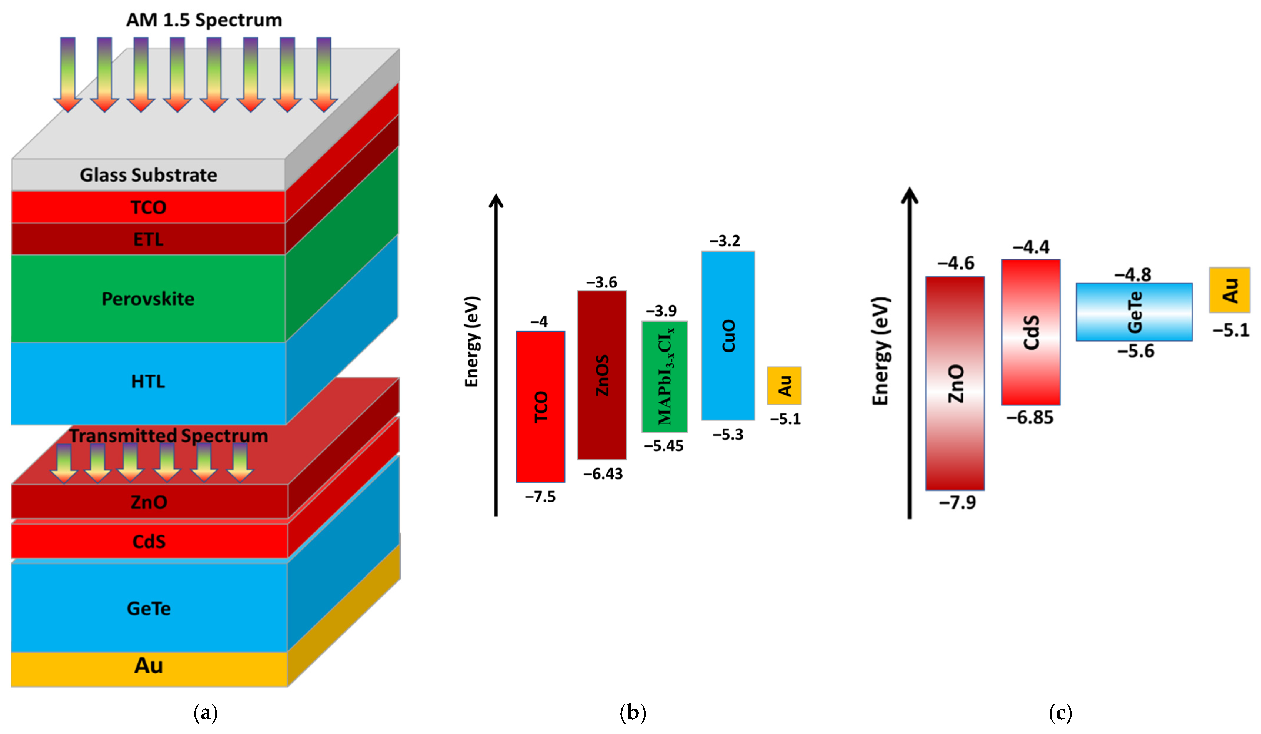
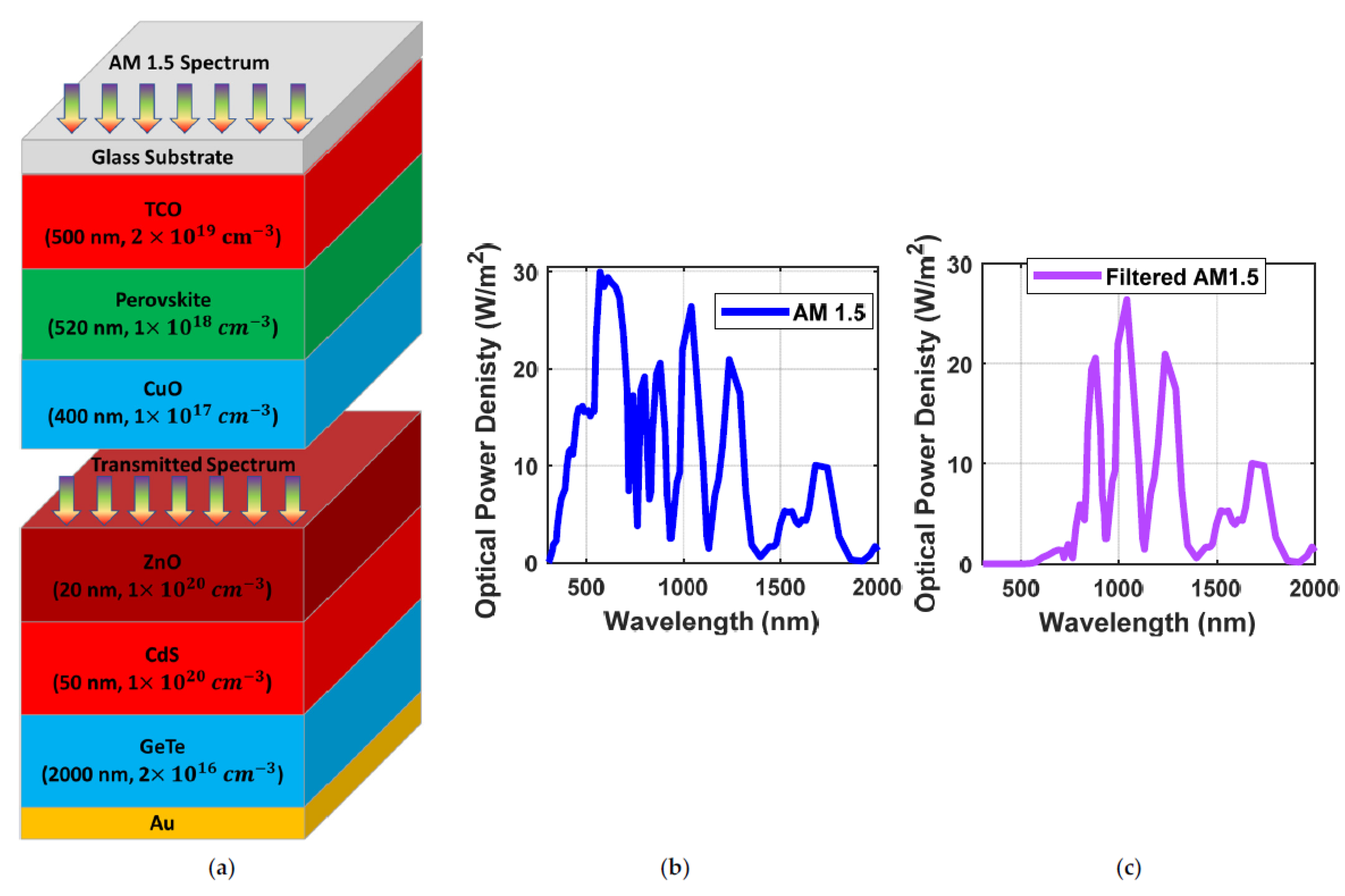
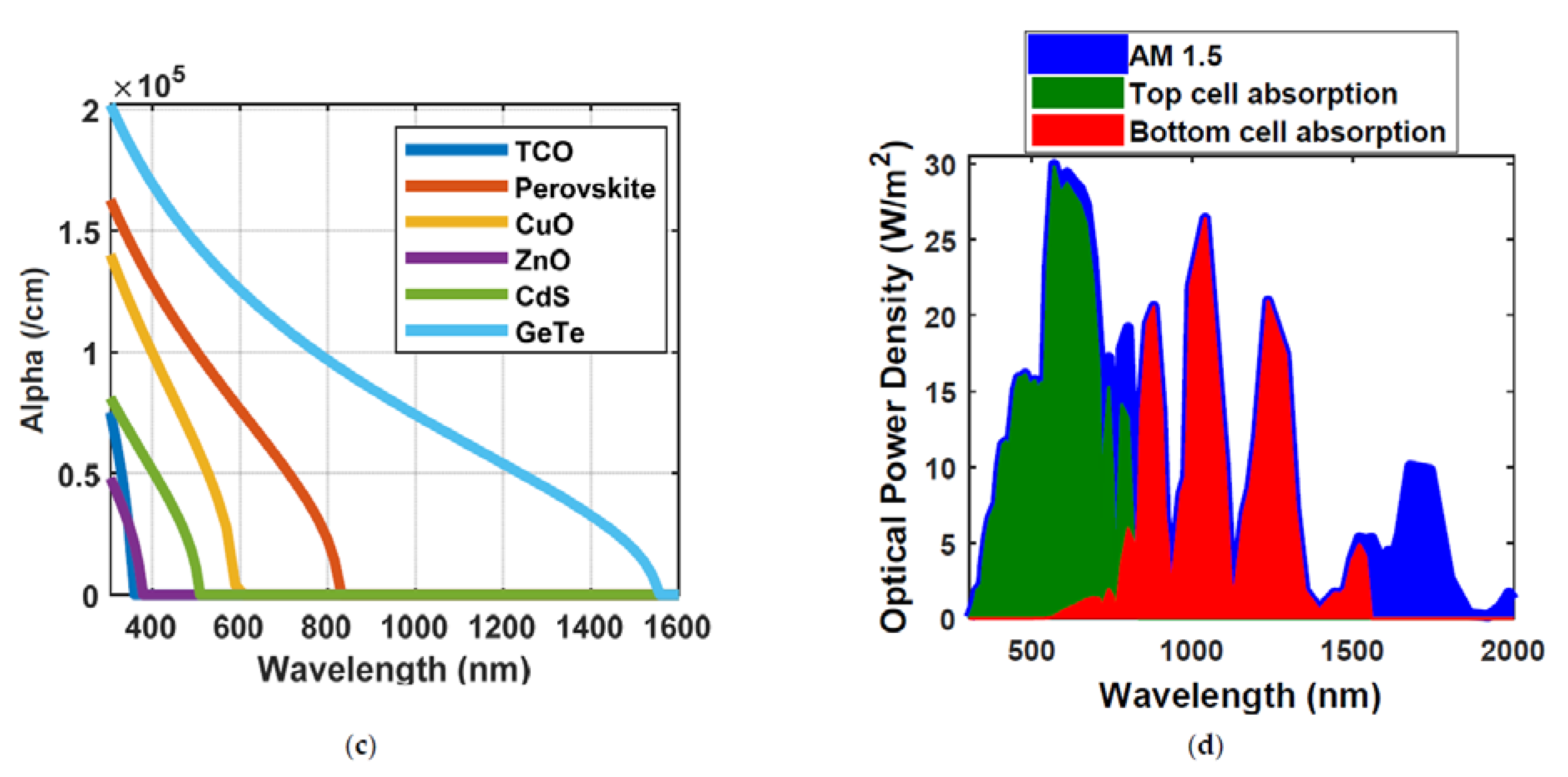
2. Tandem Solar Cell

The top and bottom sub-cells are simulated separately while investigating the performance of tandem solar cells. According to the commonly used assumption in multi-junction simulation, the tunnel junction is perfect, and the optical and electrical losses in both interfaces are neglected [18,19,20,21,22].
The proposed tandem cell consists of a PSC as a top sub-cell and a GeTe as a bottom sub-cell, as shown in Figure 1a. The structure of the top sub-cell uses the perovskite material sandwiched between the hole transport layer (HTL) and ETL. The TCO functions as an optically transparent electrode, allowing photons to pass through the cell and deliver the produced electrons to the cell’s external terminals. Before the absorber material, the bottom sub-cell consists of zinc oxide (ZnO) and cadmium sulfide (CdS). Due to its properties, especially the narrow Eg, GeTe is a good choice as an absorber of the bottom sub-cell; besides, it provides a very high current [23,24].
The transmitted spectrum of the top sub-cell to the bottom sub-cell is given by Equation (1) [18]:
S ( λ ) = S o ( λ ) · x = 1 n e α x d x  
and α is given by Equation (2) [18]:
α ( E ) = A α h ν E g  

2.1. The Top Sub-Cell

The layers of the suggested top sub-cell design are a glass substrate, fluorine-doped tin oxide (FTO) as a transparent conducting oxide (TCO), ZnOS as the ETL, CH3NH3PbI3−xCIx as an absorber layer, Cu2O as the HTL, and gold (Au) as a back contact. A common phenomenon of OSCs incorporating these metal-oxide electron extraction layers is the requirement to expose the devices to ultraviolet light to enhance the OSC performance, known as the “light soaking” issue. This issue can be avoided by using Al-doped ZnOS as electron extraction interlayers.
Figure 1b,c illustrate the energy band diagrams of the top and bottom sub-cells, respectively. The conduction band minimums are the electron affinities ( χ ) , and the valence band maximums (VBMs) are given by Equation (3).
V B M = χ E g
The parameters of the materials used in the simulation are listed in Table S2. A flat band model was employed for the interfaces between the semiconductor, TCO, and metal. To address the practical concerns, a neutral defect with Gaussian distribution was used [25]. An illumination spectrum of air mass (AM 1.5) and a temperature of 300 K were utilized for all simulations. All materials’ absorption coefficients (α) were calculated through Equation (2). The used pre-factor (Aα) was 105 cm−1eV−1/2 [26].
Figure 2 depicts the output performance curves of the first proposed PSC using Cu2O as the HTL and ZnOS as the ETL. Figure 2a shows the JV curve of the initial PSC. The values of PCE, fill factor (FF), high short-circuit current (JSC), and an open-circuit voltage (Voc) of the initial PSC were extracted from the JV curve. The designed PSC achieved a promising output performance. A PCE of 29.34% with FF of 84.88%, Jsc of 24.38 mA/cm2, and Voc of 1.42 V were obtained. The use of ZnOS as the ETL in the cell structure is consistent with the performance estimation given in [27]. These output performance metrics are achieved when the conduction band offset (CBO) of the ETM is 0.3 eV higher than the corresponding band of CH3NH3PbI3−xCIx, which is within the optimal range [28,29]. ZnOS has a tunable energy gap and a high electron affinity. Consequently, it is an excellent replacement for traditional ETMs such as titanium dioxide (TiO2).
The energy gap of ZnOS is in the range of 2.7–3.8 eV, which permits it to absorb photons with higher energy and enhances the current density [30]. Moreover, ZnOS has good transparency, which enhances photons absorption in the CH3NH3PbI3−xCIx layer, thus enhancing the output performance. Figure 2b shows the proposed PSCs’ quantum efficiency (QE) curve. The QE is almost constant in the range from 350 nm to 590 nm and subsequently falls to 800 nm, when it disappears, as seen in the curve.
The conductivity of the materials in solar cells greatly influences the performance characteristics. The conductivity of solar cell materials can be controlled by doping, either n-type or p-type. The impact of doping concentrations on CH3NH3PbI3−xCIx, ZnOS, and Cu2O is investigated through Section 2.1.1, Section 2.1.2 and Section 2.1.3 to enhance PCE.

2.1.1. Optimization of the Doping Concentration ND of CH3NH3PbI3−xCIx

The perovskite materials can be doped n-type or p-type [31]. The doping concentration can be practically adjusted between NA of 1014 cm−3 and ND of 7.6 × 1020 cm−3 [31]. The output performance metrics are constant in the NA range from 0 to 1015 cm−3. Figure 3 depicts the effect of the absorber layer’s ND on the performance metrics. The output performance metrics are constant in the ND range from 0 to 1015 cm−3. This work suggests a reasonable value of 1 × 1018 cm−3 for the perovskite layer’s ND, with a PCE of 32.19%, as displayed in Figure 3a. The PCE is enhanced by 2.83% more than the initial design. This improvement is mainly due to the enhancement in the fill factor and Voc, as depicted in Figure 3b,d, respectively. The increase in FF is due to the decrease in the series resistance as the doping rises. Additionally, it can be seen from Figure 3c that Jsc is almost constant with the variation in the doping level. The performance metrics, FF, Voc, and Jsc, when the ND of the perovskite layer is 1018 cm−3 are 90.88%, 1.45 V, and 24.38 mA/cm2, respectively.

2.1.2. Optimization of the Doping Concentration ND of ETM

The ETL does not affect the performance metrics once the absorber layer has been doped [30]. As a result, a PSC without ETL has been recommended to replace the conventional n-i-p PSC architecture with an n-p one to reduce the number of layers and interfaces. Table 1 compares the performance characteristics of the PSC with and without the ETL. Due to the imbalanced charge transfer rate and the lack of a permanent built-in field in the absence of an ETL, ETL-free perovskite solar cells suffer from significant hysteresis and unsteady stabilized-power output [32,33]. Surface modification of an FTO substrate with a self-assembled fullerene monolayer (SAM), on the other hand, can improve device performance and reduce PSC hysteresis [34,35]. FTO effects on cells can be treated by different methods, one of which was produced for PSCs in a simplified configuration of glass/FTO–TMAH/perovskite/spiro-OMeTAD/Au using a modified FTO surface with tetramethylammonium hydroxide (TMAH). The increased device performance may be attributed to the improved charge extraction/transport, lower trap density, and lower charge recombination rate at the FTO/perovskite interface and in the perovskite layer, which displays up to 20.1% efficiency experimentally [36].

2.1.3. Optimization of the Doping Concentration NA and Thickness of HTM

In a previous work, the doping concentration NA of Cu2O was increased from NA of 1017 cm−3 to 1020 cm−3 [37]. The performance metrics were low because of the high series resistance within the low doping concentration NA. When the doping in Cu2O is increased, the offset in energy bands between the perovskite layer and Cu2O layer increases, causing the diffusion current to increase due to the gradient of carrier concentrations and particles to flow from the highest concentration regions to the lowest according to random thermal motion which is known as Brownian Motion. Figure 4a depicts the effect of Cu2O NA on the PCE, while the rest of the performance parameters are illustrated in the Supplementary Materials, Figure S1. The highest PCE was achieved in the range of NA from 1017 to 1018 cm−3, as shown in Figure 4a. As a result, keeping NA at a low level is preferable. Furthermore, high NA generates deep Coulomb traps and reduces hole mobility [38]. The performance metrics, PCE, FF, Voc, and Jsc, when NA of Cu2O is 1017 cm−3 are 32.19%, 90.84%, 1.45 V, and 24.41 mA/cm2, respectively.
Following that, the effect of the HTL thickness was investigated. Figure 4b depicts the effect of Cu2O thickness on the PCE, while the rest of the performance parameters are illustrated in Figure S2. It can be shown that as the thickness of Cu2O grows from 100 to 400 nm, the PCE is almost constant. The PCE is constant for thicknesses greater than 400 nm. As a result, a thickness of 400 nm with a PCE of 32.22%, Jsc of 24.44 mA/cm2, FF of 90.83%, and no change in Voc was chosen.

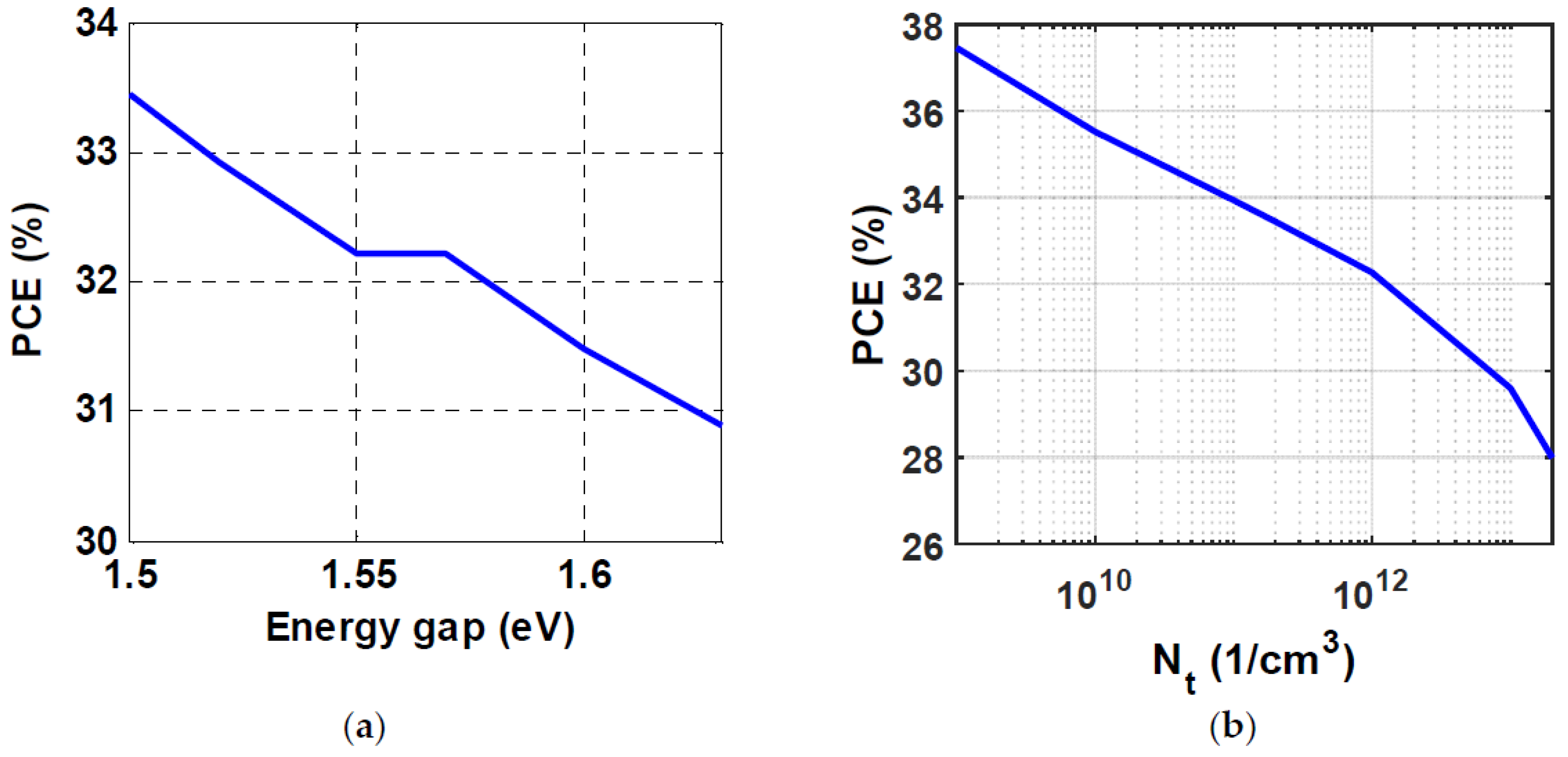
2.1.4. Impact of the Eg and Nt of CH3NH3PbI3−xCIx

The energy gap of the perovskite layer has a significant impact on the performance characteristics. PSCs benefit significantly from an adjustable energy gap. Figure 5a depicts the fluctuation in PCE caused by a change in Eg from 1.5 to 1.63 eV [39,40]. Figure S3 illustrates the rest of the performance parameters. Reducing Eg boosts carrier generation. As a result, the best performance was obtained at the lowest Eg. When Eg is 1.5 eV; the performance characteristics were as follows: PCE = 33.45%, FF = 90.58%, Voc = 1.40 V, and, Jsc = 26.30 mA/cm2 with a 3.12% increase in PCE.
The defect density has a great effect on the performance of the solar cell. Section 2.1.4 discusses the study of the defect density of the perovskite absorber layer on the main performance parameters of the PSC. The defect density was studied in the range from 109 to 2 × 10¹³ (1/cm3). The results show that the PCE decreases at a high rate with an increase in the defect density, as shown in Figure 5b. The rest of the performance metrics with the variation in the defect density are illustrated in Figure S4. The chosen defect density for our design was 2 × 10¹¹ (1/cm3). The performance parameters at this value are: PCE is 33.45%, FF is 90.58%, JSC is 26.30 mA/cm2, and VOC is 1.40 V.

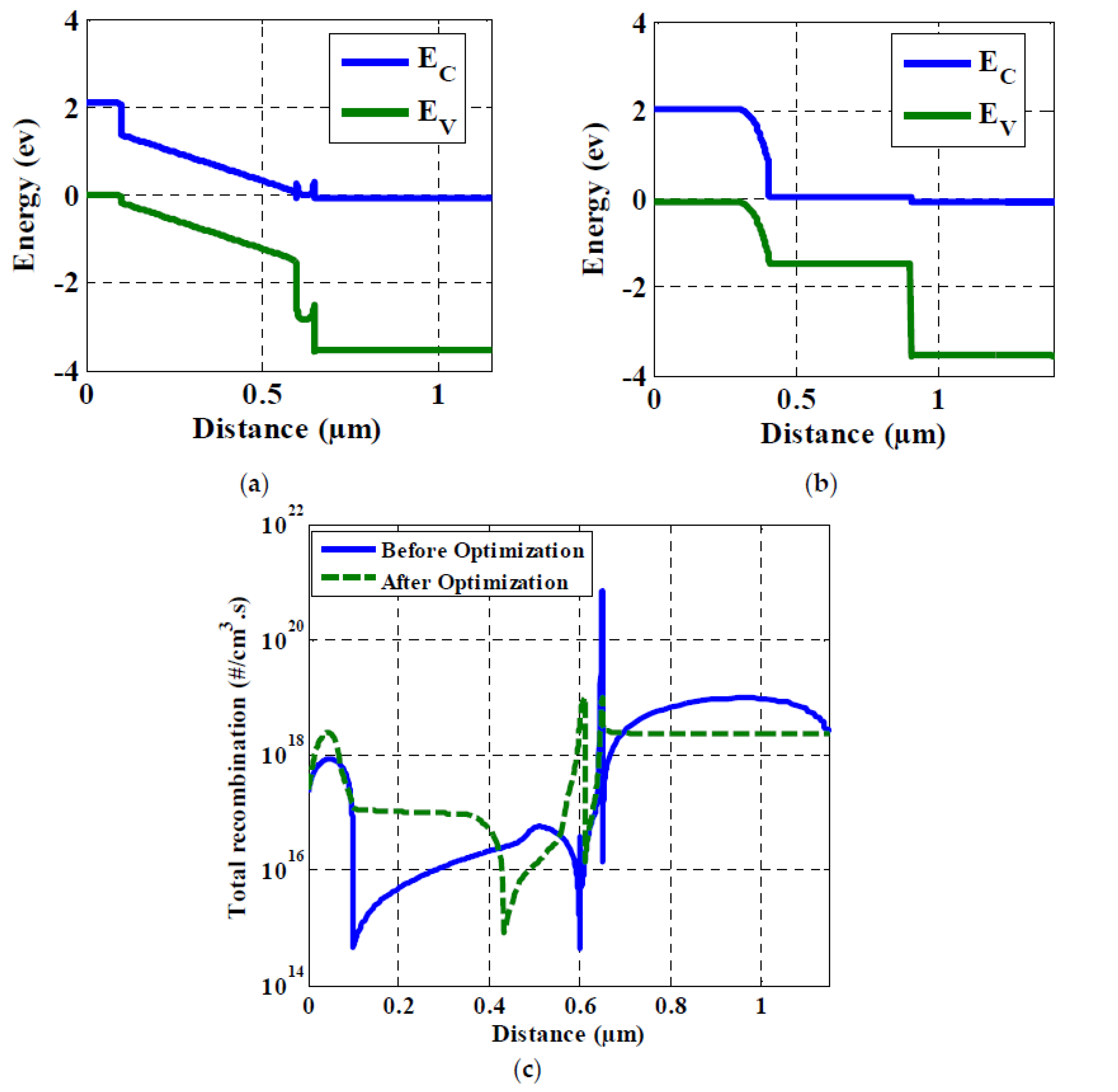
2.1.5. The Initial PSC vs. the Optimized One

Decreasing the recombination rate at the CH3NH3PbI3−xCIx/ETL interface is a good way to extract the carriers efficiently. To achieve this condition, the CBO of the CH3NH3PbI3−xCIx layer should be 0–0.3 eV lower than the corresponding band of the ETL. The CBO is given by Equation (4) [41].
CBO = ( χ abs χ ETL )
where χ abs is the affinity of the absorber layer and χ ETL is the affinity of the ETL. According to the above equation and the affinity of CH3NH3PbI3−xCIx is 3.9 eV, the optimum affinity of the ETL is in the range of 3.9–4.2 eV. This condition is not satisfied with ZnOS as an ETL because its affinity is 3.6 eV. The CBO after removing the ZnOS layer will be in the optimum range because the affinity of FTO is 4 eV, which illustrates the enhancement of the performance metrics. As an additional physical explanation of the improvement of the performance metrics, Figure 6a,b illustrates the energy band diagrams of the initial PSC and the optimized PSC without ETL. As shown in Figure 6a, the initial PSC with ZnOS as an ETL has a conduction band spike, which results in lower PCE on the other hand, the optimized PSC without ETL has a conduction band cliff, as shown in Figure 6b. The variation in the performance metrics could be explained by the observation of the recombination rate before and after optimization. Figure 6c shows the recombination rates (in cm−3 s−1) as a function of the PSC distance. As can be seen, the highest recombination rate was at the interface between CH3NH3PbI3−xCIx/ETL, which could be avoided in the optimized PSC without ETL. Moreover, the recombination rate at the interface between Cu2O/CH3NH3PbI3−xCIx was also decreased. The results support our choice of removing the ETL from the PSC and show the importance of our optimization.

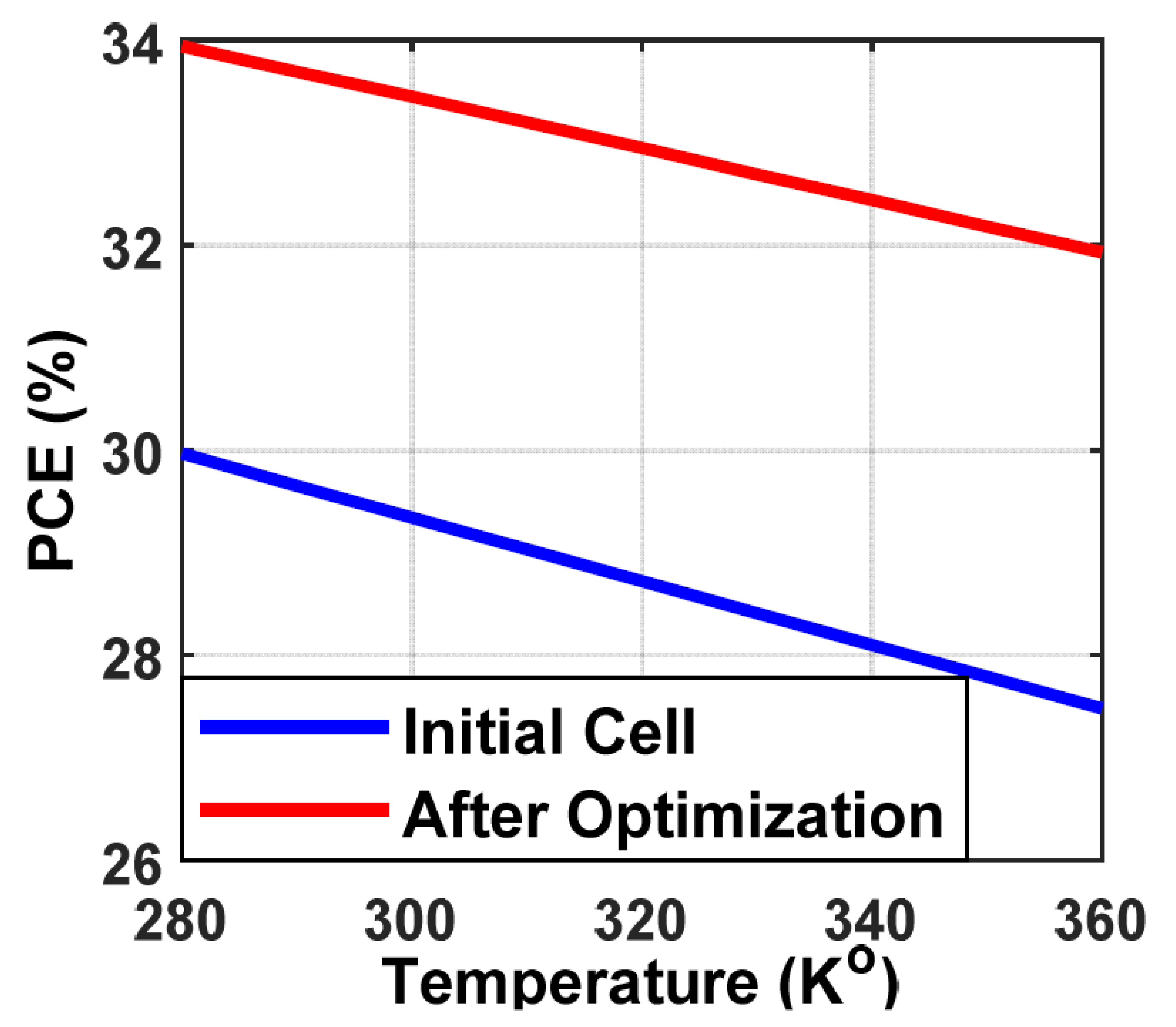
2.1.6. Temperature Effect and Comparison of PCEs

The transition from traditional to clean energy, that is, solar cells, is associated with a set of concepts. One of these concepts is to improve the unit durability to extend their lifetime [42]. PSCs still face significant commercialization challenges, including long-term durability versus environmental triggers such as temperature [43]. The temperature stability of the initial design and the optimized one were investigated from 280 to 360 K. The results show that the PCE of the optimized PSC without ETL is more stable and more immune to temperature variations than the traditional PSC with a pin structure. Figure 7 illustrates the variation in the PCE of the proposed PSCs of the initial design and the optimized PSC without ETL with temperature. At the end of this section, a comparison between the PCE for single-junction PSCs of the initial design, the optimized PSC without ETL, and other researchers’ work is shown in Table 2.

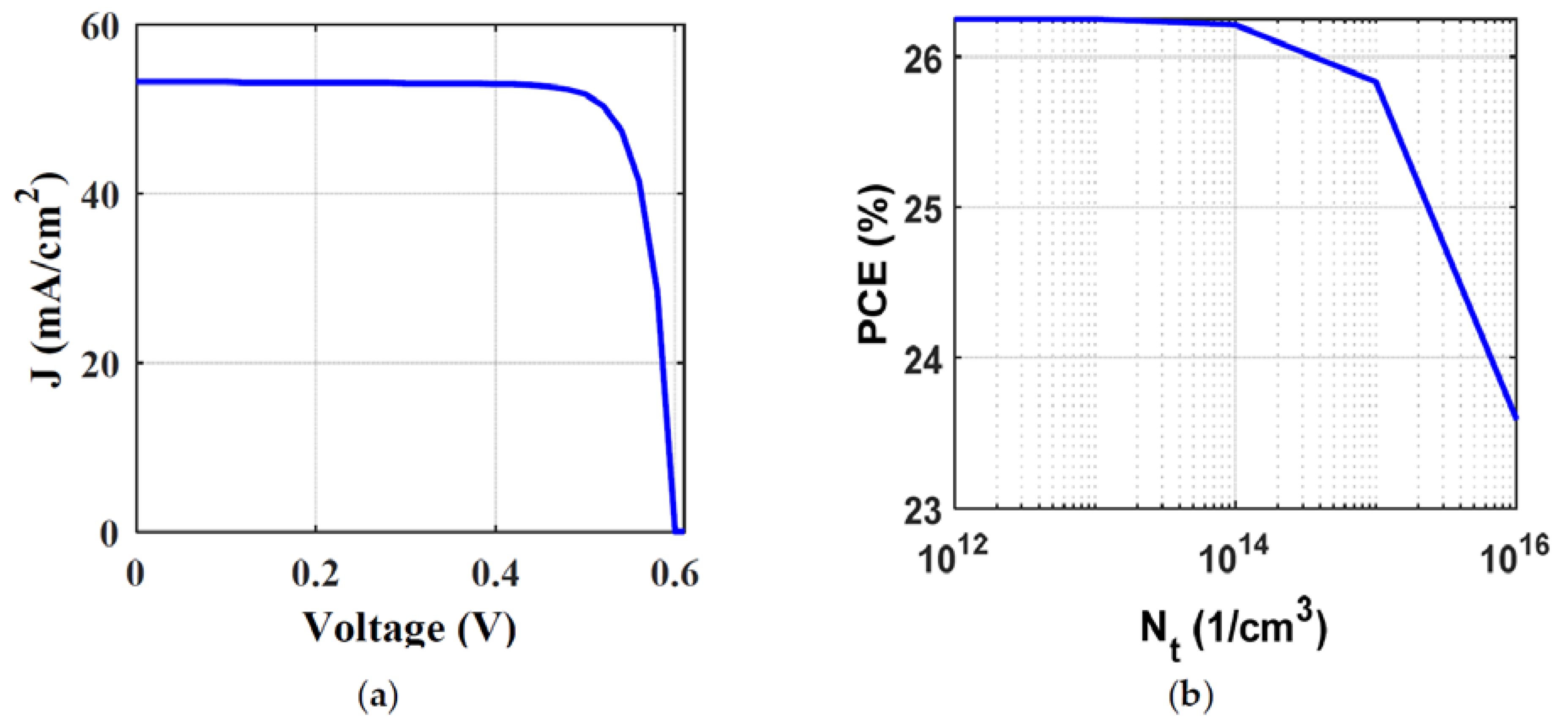
2.2. The Bottom Sub-Cell

Figure 1 illustrates the energy band diagram of the proposed bottom GeTe sub-cell. The materials parameters used in the simulation are listed in Table S3. All materials’ absorption coefficients (α) were calculated via Equation (2). The used pre-factor (Aα) was 105 cm−1eV−1/2 [26]. The JV curve using AM 1.5 incident spectrum at 300 k is shown in Figure 8a. A PCE of 26.21% with FF of 81.92%, Jsc of 53.3 mA/cm2, and Voc of 0.6 V were achieved. The defect density effect on the GeTe bottom sub-cell performance was tested in the range of 1012 to 1016 (1/cm3). The results show enhancement in the performance parameters with a decrease in the defect density but no significant decay below 1014 (1/cm3), as shown in Figure 8b of the PCE. The thickness of the GeTe layer is 2000 nm, which is quite a large thickness, to produce a defect-free film to be exploited in PV applications. Consequently, the chosen value of the designed GeTe sub-cell defect density was 1014 (1/cm3), which is a relatively high and more practical value.

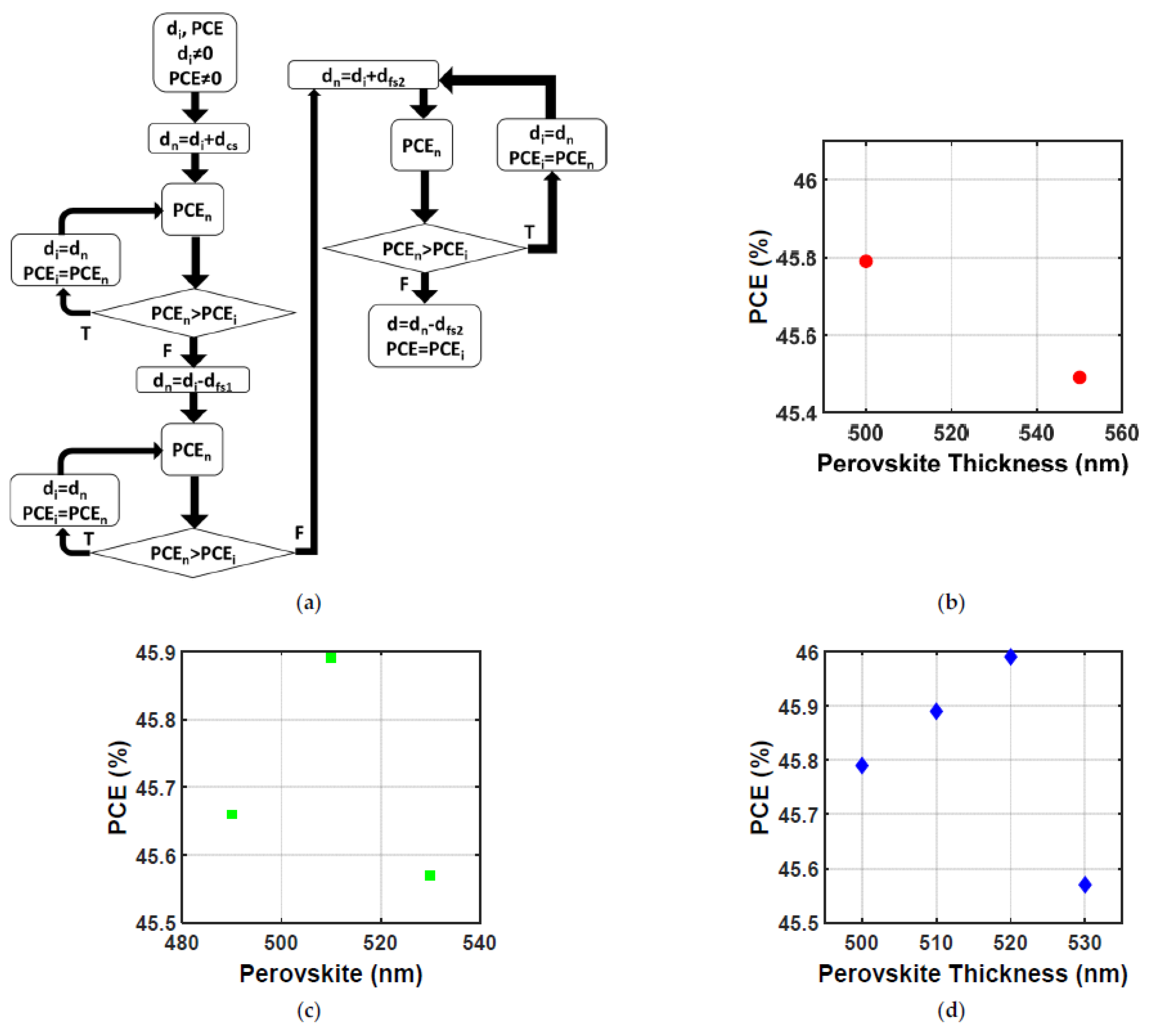
2.3. Optimizing Algorithm of the Absorber’s Thickness of the Top Sub-Cell to Achieve an Optimized Tandem Solar Cell

Two-terminal tandem solar cells have a restriction in regard to current density. The top and bottom sub-cells must have the same current density and the sub-cell with the minimum value (usually the bottom) will force the other sub-cell and the overall tandem cell to operate at its minimum current density. This, in turn, limits the overall performance of the tandem cell. The matching current density process of sub-cells is applied by changing the absorber’s thickness of the top sub-cell, as the bottom sub-cell must be as thick as possible to absorb the transmitted spectrum from the top sub-cell after a part of it is already absorbed by the top sub-cell. This section shows the proposed modification of an algorithm that optimizes the top sub-cell absorber’s thickness to get the best possible performance from the two-terminal tandem solar cells [46]. The previous algorithm uses one stage for the optimization of the thickness with one step (10 nm).
The proposed modified algorithm uses three steps: tcs (50 nm), tfs1 (20 nm), and the fine step, tfs2 (10 nm). The main difference between the proposed modified algorithm relative to the previous one is the ability to start from a high value rather than from zero, as the range of the optimum thickness range can be estimated for a tandem cell from the previous ones. Using this algorithm can decrease the number of steps to obtain the optimum thickness of the top sub-cell for the studied tandem cell, with the same accuracy of finding the thickness. This in turn decreases the processing time. The algorithm flowchart is shown in Figure 9a. It must be noted that the tandem structure’s overall thickness should not be more than the diffusion length to ensure free charge transport to electrodes, 50 µm [50].

2.4. The Optimized Tandem Solar Cell

Based on the previous results, the used top sub-cell consists of a glass substrate, TCO, N-type CH3NH3PbI3−xCIx as an absorber layer, and Cu2O as the HTL, respectively. The output spectrum from the HTL of the top sub-cell is the incident spectrum to the bottom sub-cell. The used bottom sub-cell uses GeTe as an absorber layer. The GeTe chosen to be used in the bottom sub-cell shows a high current density; this impacts the overall performance of the tandem cell current density and the tandem cell power conversion efficiency.
The top sub-cell thickness optimization algorithm explained in Section 2.3 was used to find the optimum top sub-cell absorber thickness and the highest power conversion efficiency of the tandem cell. As shown in Figure 9b–d, the tandem cell has an efficiency of 45.99% at the top sub-cell absorber layer thickness of 520 nm. A PCE of 33.61% with an FF of 90.63%, Jsc of 26.44mA/cm2, and Voc of 1.40 V were achieved by the top sub-cell using AM 1.5 incident spectrum. A PCE of 29.76% with an FF of 81.13%, Jsc of 26.67 mA/cm2, and Voc of 0.58 V were achieved by the bottom sub-cell using filtered AM 1.5 incident spectrum. The structure of the optimized tandem solar cell with complete details of the thickness and doping concentration for each layer is illustrated in Figure 10. The JV curves of both sub-cells and the tandem cell are shown in Figure 11a. Figure 11b illustrates the QE curves of both sub-cells and tandem cells. As shown in Figure 11b, the maximum light-harvesting of the tandem cell started at the wavelength of 360 µm and vanished after 1550 µm. Figure 11c shows the absorption coefficients of the materials used in the tandem cell using Equation (2), while Figure 11d shows the incident AM 1.5 with the absorbed spectrum of both sub-cells. The results show that using GeTe as a bottom sub-cell can absorb most of the transmitted spectrum up to 1540 nm. This is greater than most of the other materials that can be used as absorbers of the bottom sub-cell. This explains the improvement in the tandem cell performance.

3. Comparison with the Latest Published Results

This section outlines the recently reported results of tandem solar cells from the last few years. A comparison between this work and other published results is presented in Table 3. The proposed tandem cell has one of the highest efficiencies for double-junction tandem cells and even the more complex tandem cells with more than two junctions.

4. Conclusions

The performance of these tandem solar cells surpasses single-junction cells due to their ability to absorb a broader spectrum. The simulation of perovskite solar cells is presented in this work with ZnOS as the electron transport material and Cu2O as the hole transport material to introduce good candidates to replace the traditional materials. The perovskite solar cell without an electron transport layer was introduced to improve the stability of the top sub-cell. It has a simple design and shows excellent performance parameters. The main material parameters of the proposed Cu2O/MAPbI3−xClx perovskite solar cell without an electron transport layer were investigated to improve the performance metrics. The results obtained from the SCAPS-1D simulator show a higher open-circuit voltage of 1.404 V relative to the other recorded perovskite solar cells, which, in turn, improves the tandem cell’s overall voltage. In addition, a proposed GeTe was used as the bottom sub-cell of the tandem cell as it shows a high current density, which allows the top sub-cell to operate at a higher current density and enhances the overall two-terminal tandem cell. An optimizing algorithm was used to find the optimum top sub-cell absorber thickness. All the proposed modifications on both the top and bottom sub-cells are reflected in the power conversion efficiency of the proposed tandem cell of 46%, with an open-circuit voltage of 2.02 V and a short-circuit current density of 26.44 mA/cm2. To consider the practical concerns, the impact of a neutral defect with Gaussian distribution was investigated. This density is higher than more complicated tandem cells. To our knowledge, the proposed tandem cell shows one of the best-recorded results of the tandem cells in literature, and it is simpler than many of them.

Supplementary Materials

The following supporting information can be downloaded at: https://www.mdpi.com/article/10.3390/cryst12070878/s1, Figure S1: Performance metrics variations of the simulated PSC depending on the NA Cu2O: (a) FF, (b) Jsc, and (c) Voc; Figure S2: Performance metrics variations of the simulated PSC depending on the thickness of HTM: (a) FF, (b) Jsc, and (c) Voc; Figure S3: Performance metrics variations of the simulated PSC depending on the Eg of the absorber layer: (a) FF, (b) Jsc, and (c) Voc; Figure S4: Performance metrics variations of the simulated PSC depending on the Nt of the absorber layer: (a) FF, (b) Jsc, and (c) Voc; Table S1: Physical parameters of the incident, transmitted spectrum definitions, and their units; Table S2: Materials parameters of the top sub-cell used in SCAPS-1D simulator; Table S3. Materials parameters of the top bottom-cell used in SCAPS-1D simulator. References [3,25,30,31,45,46,57,58,59,60,61,62] are cited in the Supplementary Materials.

Author Contributions

Conceptualization, M.M.S., M.A., A.S. (Ahmed Shaker), M.M., R.I.M. and A.S. (Ahmed Saeed); methodology, M.M.S., M.A., A.S. (Ahmed Shaker), M.M., R.I.M. and A.S. (Ahmed Saeed); validation and formal analysis, M.M.S., M.A., A.S. (Ahmed Shaker), M.M., R.I.M. and A.S. (Ahmed Saeed); visualization, M.M.S. and M.M.; investigation, all authors; writing—original draft preparation, M.M.S., M.A., A.S. (Ahmed Shaker), M.M., R.I.M. and A.S. (Ahmed Saeed); writing—review and editing, all authors; supervision, A.Z., M.A., A.S. (Ahmed Shaker), F.Z.A., R.I.M. and A.S. (Ahmed Saeed). All authors have read and agreed to the published version of the manuscript.

Funding

This research received no external funding.

Institutional Review Board Statement

Not applicable.

Informed Consent Statement

Not applicable.

Data Availability Statement

No new data were created or analyzed in this study. Data sharing does not apply to this article.

Conflicts of Interest

The authors declare no conflict of interest.

References

  1. Sahbel, A.; Hassan, N.; Abdelhameed, M.M.; Zekry, A. Experimental Performance Characterization of Photovoltaic Modules Using DAQ. Energy Procedia 2013, 36, 323–332. [Google Scholar] [CrossRef] [Green Version]
  2. Fouda, S.; Salem, M.S.; Saeed, A.; Shaker, A.; Abouelatta, M. Thirteen-Level Modified Packed U-Cell Multilevel Inverter for Renewable-Energy Applications. In Proceedings of the 2020 2nd International Conference on Smart Power & Internet Energy Systems (SPIES), Bangkok, Thailand, 15–18 September 2020; pp. 431–435. [Google Scholar] [CrossRef]
  3. Masuko, K.; Shigematsu, M.; Hashiguchi, T.; Fujishima, D.; Kai, M.; Yoshimura, N.; Yamaguchi, T.; Ichihashi, Y.; Mishima, T.; Matsubara, N.; et al. Achievement of More Than 25% Conversion Efficiency With Crystalline Silicon Heterojunction Solar Cell. IEEE J. Photovolt. 2014, 4, 1433–1435. [Google Scholar] [CrossRef]
  4. Yoshikawa, K.; Kawasaki, H.; Yoshida, W.; Irie, T.; Konishi, K.; Nakano, K.; Uto, T.; Adachi, D.; Kanematsu, M.; Uzu, H.; et al. Silicon heterojunction solar cell with interdigitated back contacts for a photoconversion efficiency over 26%. Nat. Energy 2017, 2, 17032. [Google Scholar] [CrossRef]
  5. Nakamura, M.; Yamaguchi, K.; Kimoto, Y.; Yasaki, Y.; Kato, T.; Sugimoto, H. Cd-Free Cu(In,Ga)(Se,S)2 Thin-Film Solar Cell With Record Efficiency of 23.35%. IEEE J. Photovolt. 2019, 9, 1863–1867. [Google Scholar] [CrossRef]
  6. Kim, S.H.; Park, C.H.; Saeed, M.A.; Ko, D.-H.; Lee, J.-H.; Shim, J.W. β-cyclodextrin–polyacryloyl hydrazide-based surface modification for efficient electron-collecting electrodes of indoor organic photovoltaics. J. Mater. Res. Technol. 2022, 16, 1659–1666. [Google Scholar] [CrossRef]
  7. Saeed, M.A.; Cheng, S.; Biswas, S.; Kim, S.H.; Kwon, S.-K.; Kim, H.; Kim, Y.-H.; Shim, J.W. Remarkably high performance of organic photovoltaic devices with 3,9-bis(2-methylene- (3-(1,1-dicyanomethylene)-indanone))-5,5,11,11-tetrakis(4-hexyl meta-phenyl)-dithieno[2,3-d:2′,3′-d′]-s-indaceno[1,2-b:5,6-b′]dithiophene)- ethylhexyloxy] photoactive acceptor under halogen light illumination. J. Power Sources 2022, 518, 230782. [Google Scholar] [CrossRef]
  8. Saeed, M.A.; Kim, S.H.; Kim, H.; Liang, J.; Woo, H.Y.; Kim, T.G.; Yan, H.; Shim, J.W. Indoor Organic Photovoltaics: Optimal Cell Design Principles with Synergistic Parasitic Resistance and Optical Modulation Effect. Adv. Energy Mater. 2021, 11, 2003103. [Google Scholar] [CrossRef]
  9. Jia, Z.; Qin, S.; Meng, L.; Ma, Q.; Angunawela, I.; Zhang, J.; Li, X.; He, Y.; Lai, W.; Li, N.; et al. High performance tandem organic solar cells via a strongly infrared-absorbing narrow bandgap acceptor. Nat. Commun. 2021, 12, 178. [Google Scholar] [CrossRef]
  10. Yang, W.S.; Park, B.-W.; Jung, E.H.; Jeon, N.J.; Kim, Y.C.; Lee, D.U.; Shin, S.S.; Seo, J.; Kim, E.K.; Noh, J.H.; et al. Iodide management in formamidinium-lead-halide–based perovskite layers for efficient solar cells. Science 2017, 356, 1376–1379. [Google Scholar] [CrossRef] [Green Version]
  11. Salah, M.M.; Abouelatta, M.; Shaker, A.; Hassan, K.M.; Saeed, A. A comprehensive simulation study of hybrid halide perovskite solar cell with copper oxide as HTM. Semicond. Sci. Technol. 2019, 34, 115009. [Google Scholar] [CrossRef]
  12. Shockley, W.; Queisser, H.J. Detailed Balance Limit of Efficiency of p-n Junction Solar Cells. J. Appl. Phys. 1961, 32, 510–519. [Google Scholar] [CrossRef]
  13. Yasodharan, R.; Senthilkumar, A.P.; Mohankumar, P.; Ajayan, J.; Sivabalakrishnan, R. Investigation and influence of layer composition of tandem perovskite solar cells for applications in future renewable and sustainable energy. Optik 2020, 212, 164723. [Google Scholar] [CrossRef]
  14. De Vos, A. Detailed balance limit of the efficiency of tandem solar cells. J. Phys. D Appl. Phys. 1980, 13, 839–846. [Google Scholar] [CrossRef]
  15. Abdelaziz, W.; Shaker, A.; Abouelatta, M.; Zekry, A. Possible efficiency boosting of non-fullerene acceptor solar cell using device simulation. Opt. Mater. 2019, 91, 239–245. [Google Scholar] [CrossRef]
  16. Burgelman, M.; Decock, K.; Khelifi, S.; Abass, A. Advanced electrical simulation of thin film solar cells. Thin Solid Films 2013, 535, 296–301. [Google Scholar] [CrossRef]
  17. Burgelman, M.; Decock, K.; Niemegeers, A.; Verschraegen, J.; Degrave, S. SCAPS Manual; University of Ghent: Ghent, Belgium, 2016. [Google Scholar]
  18. Kim, K.; Gwak, J.; Ahn, S.K.; Eo, Y.-J.; Park, J.H.; Cho, J.-S.; Kang, M.G.; Song, H.-E.; Yun, J.H. Simulations of chalcopyrite/c-Si tandem cells using SCAPS-1D. Sol. Energy 2017, 145, 52–58. [Google Scholar] [CrossRef]
  19. Kim, K.; Yoo, J.S.; Ahn, S.K.; Eo, Y.-J.; Cho, J.-S.; Gwak, J.; Yun, J.H. Performance prediction of chalcopyrite-based dual-junction tandem solar cells. Sol. Energy 2017, 155, 167–177. [Google Scholar] [CrossRef]
  20. Gupta, G.K.; Dixit, A. Theoretical studies of single and tandem Cu2ZnSn(S/Se)4 junction solar cells for enhanced efficiency. Opt. Mater. 2018, 82, 11–20. [Google Scholar] [CrossRef]
  21. Lunardi, M.M.; Alvarez-Gaitan, J.P.; Bilbao, J.; Corkish, R.P. Life Cycle Assessment of Silicon-Based Tandem Solar Photovoltaics and their End-of-Life. Indones. J. Life Cycle Assess. Sustain. 2018, 2, 821–829. [Google Scholar] [CrossRef]
  22. Madan, J.; Shivani; Pandey, R.; Sharma, R. Device simulation of 17.3% efficient lead-free all-perovskite tandem solar cell. Sol. Energy 2020, 197, 212–221. [Google Scholar] [CrossRef]
  23. Naby, M.A.; Zekry, A.; El Akkad, F.; Ragaie, H. Dependence of dark current on zinc concentration in ZnxCd1−xS/ZnTe heterojunctions. Sol. Energy Mater. Sol. Cells 1993, 29, 97–108. [Google Scholar] [CrossRef]
  24. Salem, M.S.; Zekry, A.; Shaker, A.; Abouelatta, M.; Abdolkader, T.M. Performance enhancement of a proposed solar cell microstructure based on heavily doped silicon wafers. Semicond. Sci. Technol. 2019, 34, 035012. [Google Scholar] [CrossRef]
  25. Samiee, M.; Konduri, S.; Ganapathy, B.; Kottokkaran, R.; Abbas, H.A.; Kitahara, A.; Joshi, P.; Zhang, L.; Noack, M.; Dalal, V. Defect density and dielectric constant in perovskite solar cells. Appl. Phys. Lett. 2014, 105, 153502. [Google Scholar] [CrossRef] [Green Version]
  26. Mandadapu, U.; Vedanayakam, S.V.; Thyagarajan, K. Simulation and Analysis of Lead based Perovskite Solar Cell using SCAPS-1D. Indian J. Sci. Technol. 2017, 10, 65–72. [Google Scholar] [CrossRef]
  27. Minemoto, T.; Murata, M. Theoretical analysis on effect of band offsets in perovskite solar cells. Sol. Energy Mater. Sol. Cells 2015, 133, 8–14. [Google Scholar] [CrossRef]
  28. Abdelaziz, S.; Zekry, A.; Shaker, A.; Abouelatta, M. Investigating the performance of formamidinium tin-based perovskite solar cell by SCAPS device simulation. Opt. Mater. 2020, 101, 109738. [Google Scholar] [CrossRef]
  29. Basyoni, M.S.S.; Salah, M.M.; Mousa, M.; Shaker, A.; Zekry, A.; Abouelatta, M.; Alshammari, M.T.; Al-Dhlan, K.A.; Gontrand, C. On the Investigation of Interface Defects of Solar Cells: Lead-Based vs Lead-Free Perovskite. IEEE Access 2021, 9, 130221–130232. [Google Scholar] [CrossRef]
  30. Salem, M.S.; Salah, M.M.; Mousa, M.; Abouelatta, M.; Shaker, A.; Alzahrani, A.J.; Alanazi, A.; Ramadan, R. Efficient Perovskite Solar Cell without Electron Transport Layer. Int. J. Electr. Eng. Technol. 2021, 12, 109–117. [Google Scholar] [CrossRef]
  31. Bansal, S.; Aryal, P. Evaluation of new materials for electron and hole transport layers in perovskite-based solar cells through SCAPS-1D simulations. In Proceedings of the 2016 IEEE 43rd Photovoltaic Specialists Conference (PVSC), Portland, OR, USA, 5–10 June 2016; pp. 0747–0750. [Google Scholar] [CrossRef]
  32. Zhao, Z.; Sun, W.; Li, Y.; Ye, S.; Rao, H.; Gu, F.; Liu, Z.; Bian, Z.; Huang, C. Simplification of device structures for low-cost, high-efficiency perovskite solar cells. J. Mater. Chem. A 2017, 5, 4756–4773. [Google Scholar] [CrossRef]
  33. Yu, H.; Lee, J.W.; Yun, J.; Lee, K.; Ryu, J.; Lee, J.; Hwang, D.; Kim, S.K.; Jang, J. Outstanding Performance of Hole-Blocking Layer-Free Perovskite Solar Cell Using Hierarchically Porous Fluorine-Doped Tin Oxide Substrate. Adv. Energy Mater. 2017, 7, 1700749. [Google Scholar] [CrossRef]
  34. Valles-Pelarda, M.; Hames, B.C.; García-Benito, I.; Almora, O.; Molina-Ontoria, A.; Sánchez, R.S.; Garcia-Belmonte, G.; Martín, N.; Mora-Sero, I. Analysis of the Hysteresis Behavior of Perovskite Solar Cells with Interfacial Fullerene Self-Assembled Monolayers. J. Phys. Chem. Lett. 2016, 7, 4622–4628. [Google Scholar] [CrossRef] [PubMed] [Green Version]
  35. Topolovsek, P.; Lamberti, F.; Gatti, T.; Cito, A.; Ball, J.M.; Menna, E.; Gadermaier, C.; Petrozza, A. Functionalization of transparent conductive oxide electrode for TiO2-free perovskite solar cells. J. Mater. Chem. A 2017, 5, 11882–11893. [Google Scholar] [CrossRef]
  36. Huang, C.; Lin, P.; Fu, N.; Liu, C.; Xu, B.; Sun, K.; Wang, D.; Zeng, X.; Ke, S. Facile fabrication of highly efficient ETL-free perovskite solar cells with 20% efficiency by defect passivation and interface engineering. Chem. Commun. 2019, 55, 2777–2780. [Google Scholar] [CrossRef] [PubMed]
  37. Meyer, B.K.; Polity, A.; Reppin, D.; Becker, M.; Hering, P.; Klar, P.J.; Sander, T.; Reindl, C.; Benz, J.; Eickhoff, M.; et al. Binary copper oxide semiconductors: From materials towards devices. Phys. Status Solidi 2012, 249, 1487–1509. [Google Scholar] [CrossRef]
  38. Tan, K.; Lin, P.; Wang, G.; Liu, Y.; Xu, Z.; Lin, Y. Controllable design of solid-state perovskite solar cells by SCAPS device simulation. Solid-State Electron. 2016, 126, 75–80. [Google Scholar] [CrossRef]
  39. Chae, J.; Dong, Q.; Huang, J.; Centrone, A. Chloride Incorporation Process in CH3NH3PbI3–xClx Perovskites via Nanoscale Bandgap Maps. Nano Lett. 2015, 15, 8114–8121. [Google Scholar] [CrossRef] [Green Version]
  40. Iefanova, A.; Adhikari, N.; Dubey, A.; Khatiwada, D.; Qiao, Q. Lead free CH3NH3SnI3 perovskite thin-film with p-type semiconducting nature and metal-like conductivity. AIP Adv. 2016, 6, 085312. [Google Scholar] [CrossRef] [Green Version]
  41. Salem, M.S.; Shaker, A.; Zekry, A.; Abouelatta, M.; Alanazi, A.; Alshammari, M.T.; Gontand, C. Analysis of Hybrid Hetero-Homo Junction Lead-Free Perovskite Solar Cells by SCAPS Simulator. Energies 2021, 14, 5741. [Google Scholar] [CrossRef]
  42. Zekry, A. A road map for transformation from conventional to photovoltaic energy generation and its challenges. J. King Saud Univ.-Eng. Sci. 2020, 32, 407–410. [Google Scholar] [CrossRef]
  43. Zekry, A.; Yahyaoui, I.; Tadeo, F. Generic Analytical Models for Organic and Perovskite Solar Cells. In Proceedings of the 2019 10th International Renewable Energy Congress (IREC), Sousse, Tunisia, 26–28 March 2019; pp. 1–6. [Google Scholar] [CrossRef]
  44. Haider, S.Z.; Anwar, H.; Wang, M. A comprehensive device modelling of perovskite solar cell with inorganic copper iodide as hole transport material. Semicond. Sci. Technol. 2018, 33, 035001. [Google Scholar] [CrossRef] [Green Version]
  45. Salah, M.M.; Hassan, K.M.; Abouelatta, M.; Shaker, A. A comparative study of different ETMs in perovskite solar cell with inorganic copper iodide as HTM. Optik 2019, 178, 958–963. [Google Scholar] [CrossRef]
  46. Mousa, M.; Salah, M.M.; Amer, F.Z.; Saeed, A.; Mubarak, R.I. High Efficiency Tandem Perovskite/CIGS Solar Cell. In Proceedings of the 2020 2nd International Conference on Smart Power & Internet Energy Systems (SPIES), Bangkok, Thailand, 15–18 September 2020; pp. 224–227. [Google Scholar] [CrossRef]
  47. Wang, N.; Zhao, K.; Ding, T.; Liu, W.; Ahmed, A.S.; Wang, Z.; Tian, M.; Sun, X.; Zhang, Q. Improving Interfacial Charge Recombination in Planar Heterojunction Perovskite Photovoltaics with Small Molecule as Electron Transport Layer. Adv. Energy Mater. 2017, 7, 1700522. [Google Scholar] [CrossRef]
  48. Gu, P.-Y.; Wang, N.; Wang, C.; Zhou, Y.; Long, G.; Tian, M.; Chen, W.; Sun, X.W.; Kanatzidis, M.G.; Zhang, Q. Pushing up the efficiency of planar perovskite solar cells to 18.2% with organic small molecules as the electron transport layer. J. Mater. Chem. A 2017, 5, 7339–7344. [Google Scholar] [CrossRef]
  49. Lin, L.; Li, P.; Jiang, L.; Kang, Z.; Yan, Q.; Xiong, H.; Lien, S.; Zhang, P.; Qiu, Y. Boosting efficiency up to 25% for HTL-free carbon-based perovskite solar cells by gradient doping using SCAPS simulation. Sol. Energy 2021, 215, 328–334. [Google Scholar] [CrossRef]
  50. Rabady, R.I.; Manasreh, H. Thicknesses optimization of two- and three-junction photovoltaic cells with matched currents and matched lattice constants. Sol. Energy 2017, 158, 20–27. [Google Scholar] [CrossRef]
  51. Ferhati, H.; Djeffal, F. Exceeding 30% efficiency for an environment-friendly tandem solar cell based on earth-abundant Se/CZTS materials. Phys. E Low-Dimens. Syst. Nanostruct. 2019, 109, 52–58. [Google Scholar] [CrossRef]
  52. Benaicha, M.; Dehimi, L.; Pezzimenti, F.; Bouzid, F. Simulation analysis of a high efficiency GaInP/Si multijunction solar cell. J. Semicond. 2020, 41, 032701. [Google Scholar] [CrossRef]
  53. Cariou, R.; Benick, J.; Feldmann, F.; Höhn, O.; Hauser, H.; Beutel, P.; Razek, N.; Wimplinger, M.; Bläsi, B.; Lackner, D.; et al. III–V-on-silicon solar cells reaching 33% photoconversion efficiency in two-terminal configuration. Nat. Energy 2018, 3, 326–333. [Google Scholar] [CrossRef]
  54. Essig, S.; Allebé, C.; Remo, T.; Geisz, J.F.; Steiner, M.A.; Horowitz, K.; Barraud, L.; Ward, J.S.; Schnabel, M.; Descoeudres, A.; et al. Raising the one-sun conversion efficiency of III–V/Si solar cells to 32.8% for two junctions and 35.9% for three junctions. Nat. Energy 2017, 2, 17144. [Google Scholar] [CrossRef]
  55. Geisz, J.F.; Steiner, M.A.; Jain, N.; Schulte, K.L.; France, R.M.; McMahon, W.E.; Perl, E.E.; Friedman, D.J. Building a Six-Junction Inverted Metamorphic Concentrator Solar Cell. IEEE J. Photovolt. 2017, 8, 626–632. [Google Scholar] [CrossRef]
  56. Li, X.; Yang, J.; Jiang, Q.; Chu, W.; Zhang, D.; Zhou, Z.; Xin, J. Synergistic Effect to High-Performance Perovskite Solar Cells with Reduced Hysteresis and Improved Stability by the Introduction of Na-Treated TiO2 and Spraying-Deposited CuI as Transport Layers. ACS Appl. Mater. Interfaces 2018, 9, 41354–41362. [Google Scholar] [CrossRef] [PubMed]
  57. Mousa, M.; Amer, F.Z.; Mubarak, R.I.; Saeed, A. Simulation of Optimized High-Current Tandem Solar-Cells With Efficiency Beyond 41%. IEEE Access 2021, 9, 49724–49737. [Google Scholar] [CrossRef]
  58. Etgar, L.; Gao, P.; Xue, Z.; Peng, Q.; Chandiran, A.K.; Liu, B.; Nazeeruddin, M.K.; Grätzel, M. Mesoscopic CH 3NH 3PbI3/TiO2 heterojunction solar cells. J. Am. Chem. Soc. 2012, 134, 17396–17399. [Google Scholar] [CrossRef] [PubMed] [Green Version]
  59. Markus, G. Device Physics of Copper (Indium, Gallium) Selenide (2) Thin-Film Solar Cells. Ph.D. Thesis, Colorado State University, Fort Collins, CO, USA, 2005. [Google Scholar]
  60. Noman, M.A.A.; Abden, M.J.; Islam, M.A. Germanium telluride absorber layer, a proposal for low illumination photovoltaic application using AMPS 1D. In Proceedings of the 2018 International Conference on Computer, Communication, Chemical, Material and Electronic Engineering (IC4ME2), Rajshahi, Bangladesh, 8–9 February 2018. [Google Scholar] [CrossRef]
  61. Wagner, S.; Shay, J.L.; Migliorato, P.; Kasper, H.M. CuInSe2/CdS heterojunction photovoltaic detectors. Appl. Phys. Lett. 1974, 25, 434–435. [Google Scholar] [CrossRef]
  62. Mousa, M.; Amer, F.Z.; Saeed, A.; Mubarak, R.I. Two-Terminal Perovskite/Silicon Solar Cell: Simulation and Analysis. In Proceedings of the 2021 3rd Novel Intelligent and Leading Emerging Sciences Conference (NILES), Giza, Egypt, 23–25 October 2021; pp. 409–412. [Google Scholar] [CrossRef]
Figure 1. (a) The initial design of the proposed perovskite/GeTe tandem solar cell, (b) the energy diagrams of the top sub-cell, and (c) the bottom sub-cell.
Crystals 12 00878 g001
Figure 2. The simulated output performance curves of the proposed PSC (a) JV curve and (b) QE curve.
Crystals 12 00878 g002
Figure 3. Performance metrics’ variations in the simulated cell depending on the ND of the perovskite layer: (a) PCE, (b) FF, (c) Jsc, and (d) Voc.
Crystals 12 00878 g003
Figure 4. PCE variation in the simulated PSC depending on HTM: (a) doping and (b) thickness.
Crystals 12 00878 g004
Figure 5. PCE variation in the simulated PSC depending on the absorber layer: (a) Eg and (b) Nt.
Crystals 12 00878 g005
Figure 6. Simulated energy band diagrams: (a) of the initial PSC, (b) of the optimized PSC without ETL and (c) the recombination rates before and after optimization.
Crystals 12 00878 g006
Figure 7. Theoretical PCE of the two proposed PSCs with temperature variations: the blue line is for the initially proposed PSC cell, and the red line is for the proposed cell after removing ETL and optimization.
Crystals 12 00878 g007
Figure 8. (a) The simulated GeTe sub-cell JV curve, and (b) PCE variation in the simulated GeTe as a function of the Nt of the absorber layer.
Crystals 12 00878 g008
Figure 9. (a) Flowchart of an optimization technique for the thickness of the top cell of two junctions’ tandem cell, (b) first stage with course step (50 nm) assuming start with 500 nm thickness, (c) second stage with fine step 1 (20 nm), and (d) the third stage with course step 2 (10 nm).
Crystals 12 00878 g009
Figure 10. (a) The final simulated tandem cell after optimization, (b) as AM 1.5 illuminated on the top sub-cell, and (c) filtered AM 1.5 is illuminated on the bottom sub-cell.
Crystals 12 00878 g010
Figure 11. The output performance curves of the simulated top, and bottom sub-cells, tandem cell (a) JV curves, (b) QE curves, (c) absorption coefficients of all layers of the final tandem cell, and (d) AM 1.5 spectrum with the absorbed spectrum of top and bottom sub-cells.
Crystals 12 00878 g011aCrystals 12 00878 g011b
Table 1. Performance metrics of the simulated PSCs with and without ETL.
ETM/HTMPCE (%)Jsc (mA/cm2)Voc (V) FF (%)
ZnOS/Cu2O32.1724.3821.45290.88
-/Cu2O32.1924.4031.45190.88
Table 2. Comparison of PCEs.
ETM/HTMPCE (%)
TiO2/CuI [44]21.32
TiO2/CuI [45]21.76
ZnOS/CuI [45]26.11
ZnOS/Cu2O [11]25.71
ZnOS/Cu2O [11]30.82
PCBM/Cu2O [46]19.61
PEDOT:PSS/HATNT [47]18.1%
PEDOT:PSS/TDTP [48]18.2%
TiO2/- [49]25.15
ZnOS/Cu2O [initial]29.34
-/Cu2O [optimized]33.45
Table 3. A comparison of the latest published findings with the optimized tandem cell.
PCE (%)Jsc (mA/cm2)Voc (V) FFThe Material of Top/Bottom Sub-CellsRef.—YearType of Analysis
30.222.41.9468.90Se/CZTSSe[51]—2019Exp.
30.520.491.8181.90MAPbI3/CIGS[46]—2020Exp.
31.117.042.0788.00GaInP/Si[52]—2020Exp.
33.312.73.12783.50Triple-junction (Ga0.51 In0.49 P/GaAs/Si)[53]—2018Exp.
35.913.62.5287.50Triple-junction (GaInP/GaAs/Si)[54]—2017Exp.
35.925.881.74779.40MAPbI3/GeTe[55]—2021Sim.
39.28.4575.54983.50Six junction (monolithic)[56]—2017Exp.
41.7326.54 1.83585.66MAPbI3−xClx/GeTe[57]—2021Sim.
45.9926.442.0286.11MAPbI3−xClx without ETL/GeTeThis workSim.
Publisher’s Note: MDPI stays neutral with regard to jurisdictional claims in published maps and institutional affiliations.

