
Process of Au-Free Source/Drain Ohmic Contact to AlGaN/GaN HEMT

 ,
,
Abstract
:1. Introduction
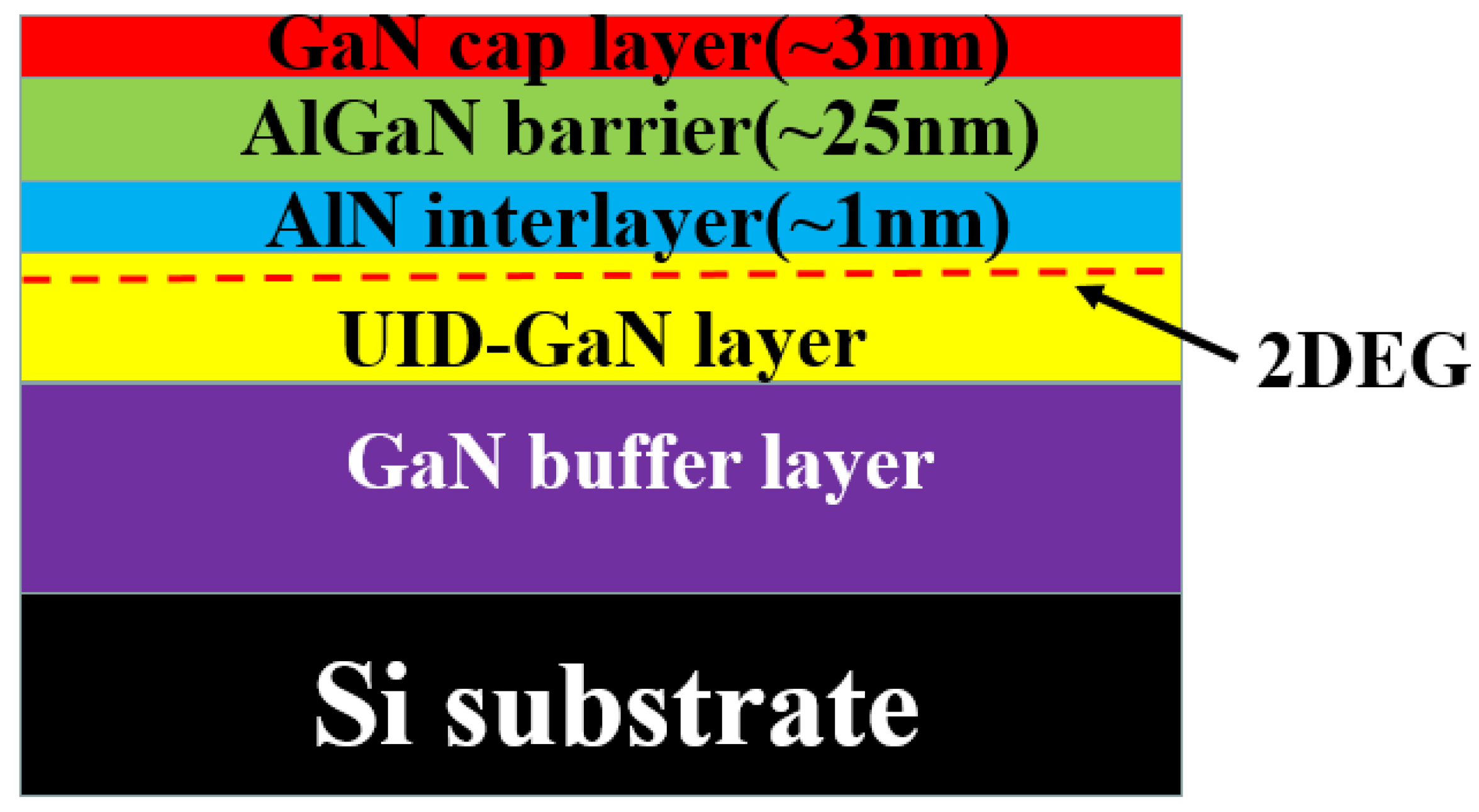
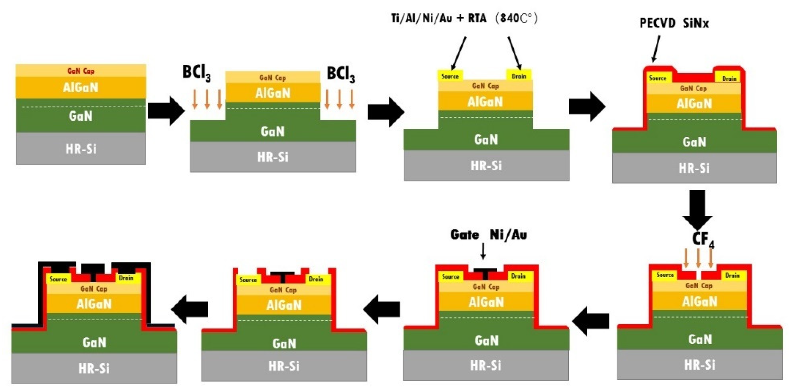
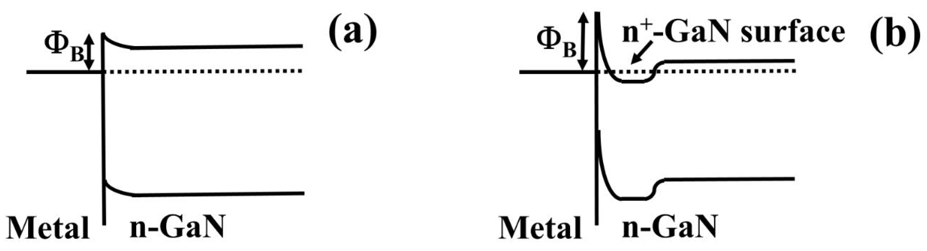
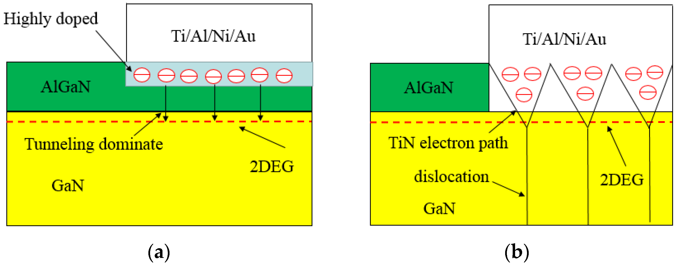
2. Ti/Al/X/Au Au-Contained Ohmic Contact Technique
3. Au-Free Ohmic Contact Technique
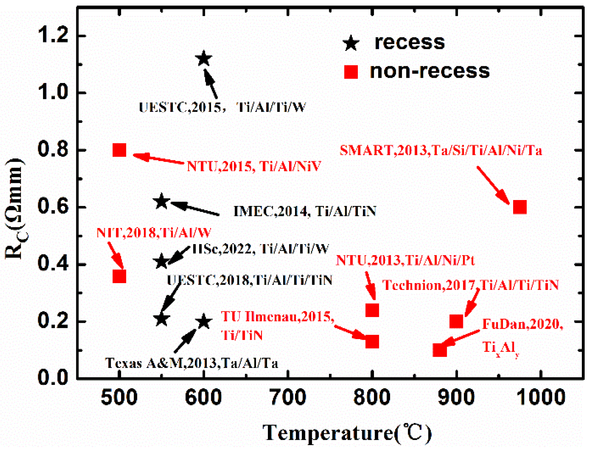
3.1. Existing Advanced Au-Free Ohmic Contact Technology
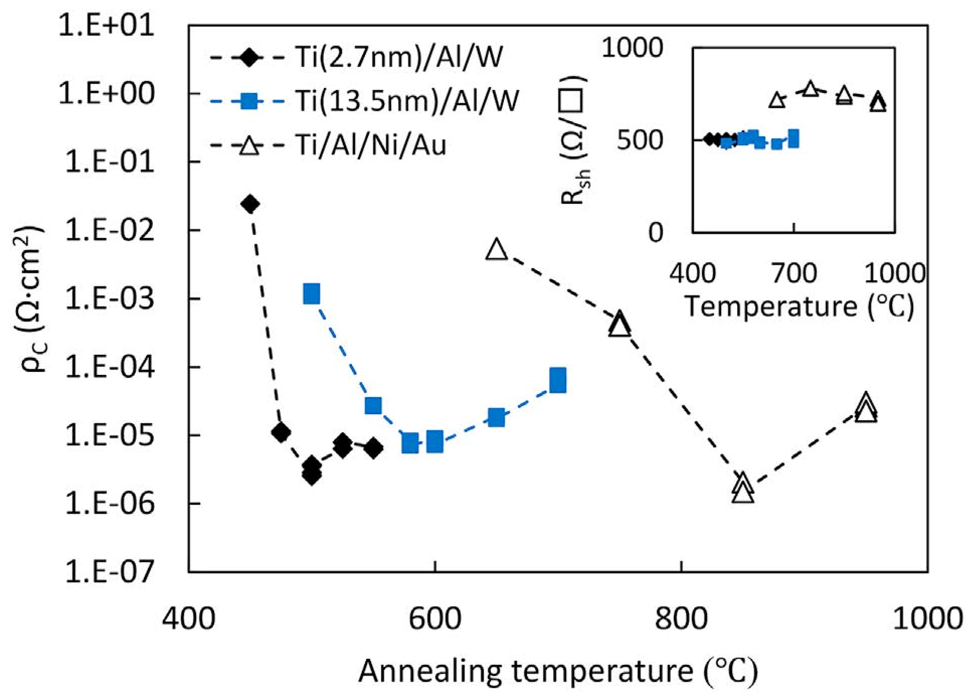
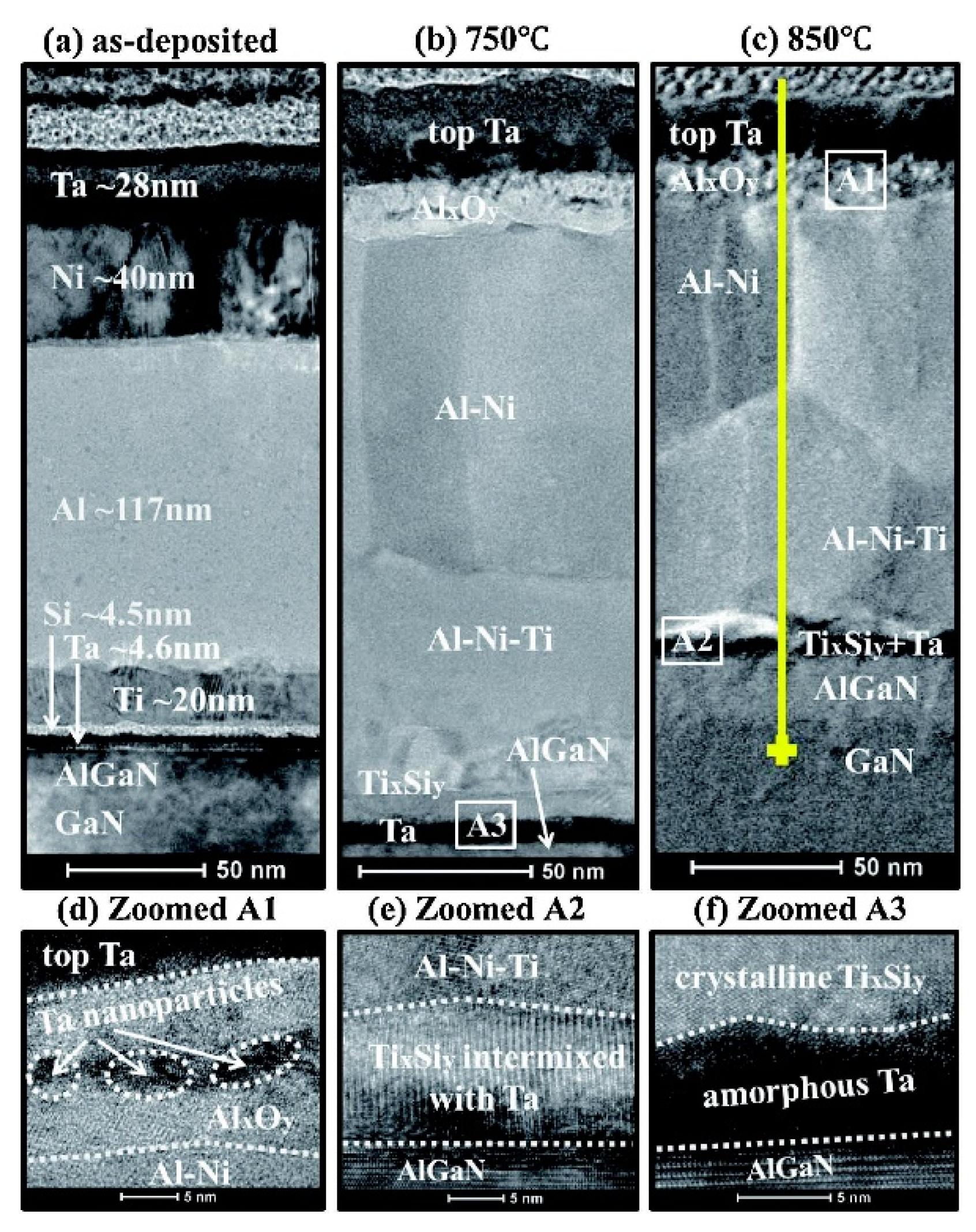
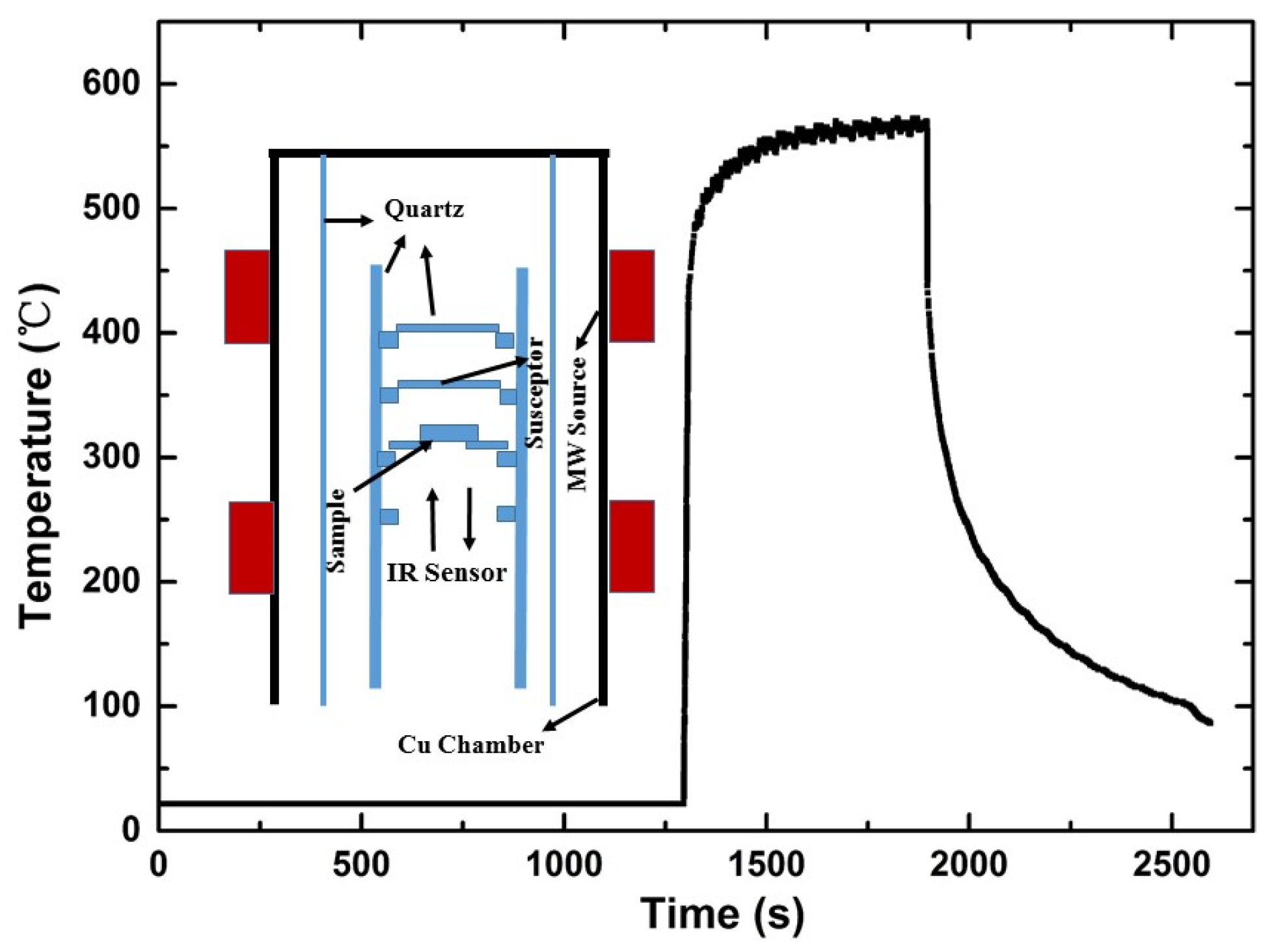
3.2. Low-Temperature Au-Free Ohmic Contact Technology
4. Conclusions
Author Contributions
Funding
Institutional Review Board Statement
Informed Consent Statement
Data Availability Statement
Conflicts of Interest
References
- Chen, K.J.; Häberlen, O.; Lidow, A.; lin Tsai, C.; Ueda, T.; Uemoto, Y.; Wu, Y. GaN-on-Si power technology: Devices and applications. IEEE Trans. Electron Devices 2017, 64, 779–795. [Google Scholar] [CrossRef]
- He, J.; Cheng, W.C.; Wang, Q.; Cheng, K.; Yu, H.; Chai, Y. Recent Advances in GaN-Based Power HEMT Devices. Adv. Electron. Mater. 2021, 7, 2001045. [Google Scholar] [CrossRef]
- Mishra, U.K.; Shen, L.; Kazior, T.E.; Wu, Y.F. GaN-based RF power devices and amplifiers. Proc. IEEE 2008, 96, 287–305. [Google Scholar] [CrossRef]
- Palacios, T.; Chakraborty, A.; Rajan, S.; Poblenz, C.; Keller, S.; DenBaars, S.P.; Speck, J.S.; Mishra, U.K. High-power AlGaN/GaN HEMTs for ka-band applications. IEEE Electron Device Lett. 2005, 26, 781–783. [Google Scholar] [CrossRef] [Green Version]
- Pengelly, R.S.; Wood, S.M.; Milligan, J.W.; Sheppard, S.T.; Pribble, W.L. A review of GaN on SiC high electron-mobility power transistors and MMICs. IEEE Trans. Microw. Theory Tech. 2012, 60, 1764–1783. [Google Scholar] [CrossRef]
- Pérez-Tomás, A.; Fontserè, A.; Llobet, J.; Placidi, M.; Rennesson, S.; Baron, N.; Chenot, S.; Moreno, J.C.; Cordier, Y. Analysis of the AlGaN/GaN vertical bulk current on Si, sapphire, and free-standing GaN substrates. J. Appl. Phys. 2013, 113, 174501. [Google Scholar] [CrossRef]
- Liang, Z.; Du, H.; Yuan, Y.; Wang, Q.; Kang, J.; Zhou, H.; Zhang, J.; Hao, Y.; Wang, X.; Zhang, G. Ultra-thin AlGaN/GaN HFET with a high breakdown voltage on sapphire substrates. Appl. Phys. Lett. 2021, 119, 252101. [Google Scholar] [CrossRef]
- Ishida, M.; Ueda, T.; Tanaka, T.; Ueda, D. GaN on Si technologies for power switching devices. IEEE Trans. Electron Devices 2013, 60, 3053–3059. [Google Scholar] [CrossRef]
- Wośko, M.; Szymański, T.; Paszkiewicz, B.; Pokryszka, P.; Paszkiewicz, R. MOVPE growth conditions optimization for AlGaN/GaN/Si heterostructures with SiN and LT-AlN interlayers designed for HEMT applications. J. Mater. Sci. Mater. Electron. 2019, 30, 4111–4116. [Google Scholar] [CrossRef] [Green Version]
- Baliga, B.J. Power semiconductor device figure of merit for high-frequency applications. IEEE Electron Device Lett. 1989, 10, 455–457. [Google Scholar] [CrossRef]
- Tang, Y.; Shinohara, K.; Regan, D.; Corrion, A.; Brown, D.; Wong, J.; Schmitz, A.; Fung, H.; Kim, S.; Micovic, M. Ultrahigh-speed GaN high-electron-mobility transistors with fT/fmax of 454/444 GHz. IEEE Electron Device Lett. 2015, 36, 549–551. [Google Scholar] [CrossRef]
- Su, M.; Chen, C.; Rajan, S. Prospects for the application of GaN power devices in hybrid electric vehicle drive systems. Semicond. Sci. Technol. 2013, 28, 074012. [Google Scholar] [CrossRef]
- Freedsman, J.J.; Egawa, T.; Yamaoka, Y.; Yano, Y.; Ubukata, A.; Tabuchi, T.; Matsumoto, K. Normally-off Al2O3/AlGaN/GaN MOS-HEMT on 8 in. Si with low leakage current and high breakdown voltage (825 V). Appl. Phys. Express 2014, 7, 041003. [Google Scholar] [CrossRef]
- Egawa, T. Heteroepitaxial growth and power electronics using AlGaN/GaN HEMT on Si. In Proceedings of the 2012 International Electron Devices Meeting, San Francisco, CA, USA, 10–13 December 2012. [Google Scholar]
- Then, H.W.; Radosavljevic, M.; Agababov, P.; Ban, I.; Bristol, R.; Chandhok, M.; Chouksey, S.; Holybee, B.; Huang, C.Y.; Krist, B.; et al. GaN and Si Transistors on 300mm Si (111) Enabled by 3D Monolithic Heterogeneous Integration. In Proceedings of the 2020 IEEE Symposium on VLSI Technology, Honolulu, HI, USA, 16–19 June 2020; pp. 1–2. [Google Scholar]
- Asbeck, P.M.; Yu, E.T.; Lau, S.S.; Sullivan, G.J.; Van Hove, J.; Redwing, J. Piezoelectric charge densities in AlGaN/GaN HFETs. Electron. Lett. 1997, 33, 1230–1231. [Google Scholar] [CrossRef]
- Katz, O.; Horn, A.; Bahir, G.; Salzman, J. Electron mobility in an AlGaN/GaN two-dimensional electron gas. I. Carrier concentration dependent mobility. IEEE Trans. Electron Devices 2003, 50, 2002–2008. [Google Scholar] [CrossRef]
- Jessen, G.H.; Fitch, R.C.; Gillespie, J.K.; Via, G.; Crespo, A.; Langley, D.; Denninghoff, D.J.; Trejo, M.; Heller, E.R. Short-channel effect limitations on high-frequency operation of AlGaN/GaN HEMTs for T-gate devices. IEEE Trans. Electron Devices 2007, 54, 2589–2597. [Google Scholar] [CrossRef]
- Ranjan, K.; Arulkumaran, S.; Ng, G.I.; Vicknesh, S. High Johnson’s figure of merit (8.32 THz· V) in 0.15-µm conventional T-gate AlGaN/GaN HEMTs on silicon. Appl. Phys. Express 2014, 7, 044102. [Google Scholar] [CrossRef]
- Androse, D.R.; Deb, S.; Radhakrishnan, S.K.; Sekar, E. T-gate AlGaN/GaN HEMT with effective recess engineering for enhancement mode operation. Mater. Today Proc. 2021, 45, 3556–3559. [Google Scholar] [CrossRef]
- Tasker, P.J.; Hughes, B. Importance of source and drain resistance to the maximum fT of millimeter-wave MODFETs. IEEE Electron Device Lett. 1989, 10, 291–293. [Google Scholar] [CrossRef]
- Li, L.; Nomoto, K.; Pan, M.; Li, W.S.; Hickman, A.; Miller, J.; Lee, K.; Hu, Z.Y.; Bader, S.J.; Lee, S.M.; et al. GaN HEMTs on Si with regrown contacts and cutoff/maximum oscillation frequencies of 250/204 GHz. IEEE Electron Device Lett. 2020, 41, 689–692. [Google Scholar] [CrossRef]
- Shinohara, K.; Corrion, A.; Regan, D.; Milosavljevic, I.; Brown, D.; Burnham, S.; Willadsen, P.J.; Butler, C.; Schmitz, A.; Wheeler, D.; et al. 220GHz fT and 400GHz fmax in 40-nm GaN DH-HEMTs with re-grown ohmic. In Proceedings of the 2010 International Electron Devices Meeting, San Francisco, CA, USA, 6–8 December 2010. [Google Scholar]
- Brown, D.F.; Shinohara, K.; Corrion, A.L.; Chu, R.; Williams, A.; Wong, J.C.; Rodriguez, I.A.; Grabar, R.; Johnson, M.; Butler, C.M.; et al. High-Speed, Enhancement-Mode GaN Power Switch with Regrown n+ GaN Ohmic Contacts and Staircase Field Plates. IEEE Electron Device Lett. 2013, 34, 1118–1120. [Google Scholar] [CrossRef]
- Zhang, L.Q.; Huang, H.F.; Liu, X.Y.; Shi, J.S.; Liu, Z.; Zhao, S.X.; Wang, P.F. Two-dimensional device simulation for radio frequency performance of AlGaN/GaN HEMT, Semiconductor Technology International Conference. In Proceedings of the 2015 China Semiconductor Technology International Conference, Shanghai, China, 15–16 March 2015; pp. 1–3. [Google Scholar]
- Fontserè, A.; Pérez-Tomás, A.; Placidi, M.; Llobet, J.; Baron, N.; Chenot, S.; Cordier, Y.; Moreno, J.C.; Gammon, P.M.; Jennings, M.R.; et al. Micro and nano analysis of 0.2 Ω mm Ti/Al/Ni/Au ohmic contact to AlGaN/GaN. Appl. Phys. Lett. 2011, 99, 213504. [Google Scholar] [CrossRef]
- Wang, C.; Kim, N.Y. Electrical characterization and nanoscale surface morphology of optimized Ti/Al/Ta/Au ohmic contact for AlGaN/GaN HEMT. Nanoscale Res. Lett. 2012, 7, 1–8. [Google Scholar] [CrossRef] [PubMed] [Green Version]
- Wang, L.; Mohammed, F.M.; Adesida, I. Dislocation-induced nonuniform interfacial reactions of Ti/Al/Mo/Au ohmic contacts on AlGaN/GaN heterostructure. Appl. Phys. Lett. 2005, 87, 141915. [Google Scholar] [CrossRef]
- Shen, B.; Zhou, H.M.; Liu, J.; Zhou, Y.G.; Zhang, R.; Shi, Y.; Zheng, Y.D.; Someya, T.; Arakawa, Y. Ohmic contact and interfacial reaction of Ti/Al/Pt/Au metallic multi-layers on n-AlxGa1− xN/GaN heterostructures. Opt. Mater. 2003, 23, 197–201. [Google Scholar] [CrossRef]
- Mohammed, F.M.; Wang, L.; Adesida, I.; Piner, E. The role of barrier layer on Ohmic performance of Ti/Al-based contact metallizations on AlGaN/GaN heterostructures. J. Appl. Phys. 2006, 100, 023708. [Google Scholar] [CrossRef]
- Piazza, M.; Dua, C.; Oualli, M.; Morvan, E.; Carisetti, D.; Wyczisk, F. Degradation of TiAlNiAu as ohmic contact metal for GaN HEMTs. Microelectron. Reliab. 2009, 49, 1222–1225. [Google Scholar] [CrossRef]
- Roccaforte, F.; Iucolano, F.; Giannazzo, F.; Alberti, A.; Raineri, V. Nanoscale carrier transport in Ti/Al/Ni/Au Ohmic contacts on AlGaN epilayers grown on Si (111). Appl. Phys. Lett. 2006, 89, 022103. [Google Scholar] [CrossRef]
- Yoshida, T.; Egawa, T. Improvement of Au-Free, Ti/Al/W Ohmic Contact on AlGaN/GaN Heterostructure Featuring a Thin-Ti Layer and Low Temperature Annealing. Phys. Status Solidi A 2018, 215, 1700825. [Google Scholar] [CrossRef]
- Ganchenkova, M.G.; Nieminen, R.M. Nitrogen vacancies as major point defects in gallium nitride. Phys. Rev. Lett. 2006, 96, 196402. [Google Scholar] [CrossRef] [Green Version]
- Islam, Z.; Haque, A.; Glavin, N. Real-time visualization of GaN/AlGaN high electron mobility transistor failure at off-state. Appl. Phys. Lett. 2018, 113, 183102. [Google Scholar] [CrossRef]
- Gong, R.; Wang, J.; Liu, S.; Dong, Z.; Yu, M.; Wen, C.; Cai, Y.; Zhang, B. Analysis of surface roughness in Ti/Al/Ni/Au Ohmic contact to AlGaN/GaN high electron mobility transistors. Appl. Phys. Lett. 2010, 97, 062115. [Google Scholar] [CrossRef]
- Saadat, O.I.; Chung, J.W.; Piner, E.L.; Palacios, T. Gate-first AlGaN/GaN HEMT technology for high-frequency applications. IEEE Electron Device Lett. 2009, 30, 1254–1256. [Google Scholar] [CrossRef]
- Rickert, K.A.; Ellis, A.B.; Kim, J.K.; Lee, J.L.; Himpsel, F.J.; Dwikusuma, F.; Kuech, T.F. X-ray photoemission determination of the Schottky barrier height of metal contacts to n-GaN and p-GaN. J. Appl. Phys. 2002, 92, 6671–6678. [Google Scholar] [CrossRef] [Green Version]
- Hirsch, M.T.; Duxstad, K.J.; Haller, E.E. Effects of annealing on Ti Schottky barriers on n-type GaN. Electron. Lett. 1997, 33, 95–96. [Google Scholar] [CrossRef]
- Binari, S.C.; Dietrich, H.B.; Kelner, G.; Rowland, L.B.; Doverspike, K.; Gaskill, D.K. Electrical characterisation of Ti Schottky barriers on n-type GaN. Electron. Lett. 1994, 30, 909–911. [Google Scholar] [CrossRef]
- Lee, M.L.; Sheu, J.K.; Lin, S.W. Schottky barrier heights of metal contacts to n-type gallium nitride with low-temperature-grown cap layer. Appl. Phys. Lett. 2006, 88, 032103. [Google Scholar] [CrossRef]
- Reddy, V.R.; Ramesh, C.K.; Choi, C.J. Structural and electrical properties of Mo/n-GaN Schottky diodes. Phys. Status Solidi A 2006, 203, 622–627. [Google Scholar] [CrossRef]
- Wu, Y.F.; Jiang, W.N.; Keller, B.P.; Keller, S.; Kapolnek, D.; Denbaars, S.P.; Mishra, U.K.; Wilson, B. Low resistance ohmic contact to n-GaN with a separate layer method. Solid-State Electron. 1997, 41, 165–168. [Google Scholar] [CrossRef]
- Schmitz, A.C.; Ping, A.T.; Khan, M.A.; Chen, Q.; Yang, J.W.; Adesida, I. Metal contacts to n-type GaN. J. Electron. Mater. 1998, 27, 255–260. [Google Scholar] [CrossRef]
- Luther, B.P.; Mohney, S.E.; Jackson, T.N.; Asif Khan, M.; Chen, Q.; Yang, J.W. Investigation of the mechanism for Ohmic contact formation in Al and Ti/Al contacts to n-type GaN. Appl. Phys. Lett. 1997, 7, 57–59. [Google Scholar] [CrossRef] [Green Version]
- Ping, A.T.; Khan, M.A.; Adesida, I. Ohmic contacts to n-type GaN using Pd/Al metallization. J. Electron. Mater. 1996, 25, 819–824. [Google Scholar] [CrossRef]
- Fan, Z.; Mohammad, S.N.; Kim, W.; Aktas, Ö.; Botchkarev, A.E.; Morkoç, H. Very low resistance multilayer Ohmic contact to n-GaN. Appl. Phys. Lett. 1996, 68, 1672–1674. [Google Scholar] [CrossRef] [Green Version]
- Wang, L.; Mohammed, F.M.; Adesida, I. Differences in the reaction kinetics and contact formation mechanisms of annealed Ti/Al/Mo/Au Ohmic contacts on n-Ga N and AlGaN/GaN epilayers. J. Appl. Phys. 2007, 101, 013702. [Google Scholar] [CrossRef]
- Luther, B.P.; Mohney, S.E.; Jackson, T.N. Titanium and titanium nitride contacts to n-type gallium nitride. Semicond. Sci. Technol. 1998, 13, 1322. [Google Scholar] [CrossRef]
- Kim, J.K.; Jang, H.W.; Lee, J.L. Mechanism for Ohmic contact formation of Ti on n-type GaN investigated using synchrotron radiation photoemission spectroscopy. J. Appl. Phys. 2002, 91, 9214–9217. [Google Scholar] [CrossRef]
- Van Daele, B.; Van Tendeloo, G.; Ruythooren, W.; Derluyn, J.; Leys, M.R.; Germain, M. The role of Al on Ohmic contact formation on n-type GaN and AlGaN/GaN. Appl. Phys. Lett. 2005, 87, 061905. [Google Scholar] [CrossRef]
- Mohammed, F.M.; Wang, L.; Selvanathan, D.; Hu, H.; Adesida, I. Ohmic contact formation mechanism of Ta/Al/Mo/Au and Ti/Al/Mo/Au metallizations on AlGaN/GaN HEMTs. J. Vac. Sci. Technol. B Microelectron. Nanometer Struct. Processing Meas. Phenom. 2005, 23, 2330–2335. [Google Scholar] [CrossRef]
- Qin, Z.X.; Chen, Z.Z.; Tong, Y.Z.; Ding, X.M.; Hu, X.D.; Yu, T.J.; Zhang, G.Y. Study of Ti/Au, Ti/Al/Au, and Ti/Al/Ni/Au ohmic contacts to n-GaN. Appl. Phys. A Mater. Sci. Processing 2004, 78, 729–731. [Google Scholar] [CrossRef]
- Jacobs, B.; Kramer, M.; Geluk, E.J.; Karouta, F. Optimization of the Ti/Al/Ni/Au ohmic contact on AlGaN/GaN FET structures. J. Cryst. Growth 2002, 241, 15–18. [Google Scholar] [CrossRef]
- Kong, X.; Wei, K.; Liu, G.; Liu, X. Role of Ti/Al relative thickness in the formation mechanism of Ti/Al/Ni/Au Ohmic contacts to AlGaN/GaN heterostructures. J. Phys. D Appl. Phys. 2012, 45, 265101. [Google Scholar] [CrossRef]
- Feng, Q.; Li, L.M.; Hao, Y.; Ni, J.Y.; Zhang, J.C. The improvement of ohmic contact of Ti/Al/Ni/Au to AlGaN/GaN HEMT by multi-step annealing method. Solid-State Electron. 2009, 53, 955–958. [Google Scholar] [CrossRef]
- Yu, H.; McCarthy, L.; Rajan, S.; Keller, S.; Denbaars, S.; Speck, J.; Mishra, U. Ion implanted AlGaN-GaN HEMTs with nonalloyed ohmic contacts. IEEE Electron Device Lett. 2005, 26, 283–285. [Google Scholar]
- Brown, D.F.; Williams, A.; Shinohara, K.; Kurdoghlian, A.; Milosavljevic, I.; Hashimoto, P.; Grabar, R.; Burnham, S.; Bulter, C.; Willadsen, P. W-band power performance of AlGaN/GaN DHFETs with regrown n+ GaN ohmic contacts by MBE. In Proceedings of the International Electron Devices Meeting, Washington, DC, USA, 5–7 December 2011. [Google Scholar]
- Yan, W.; Zhang, R.; Du, Y.; Han, W.; Yang, F. Analysis of the ohmic contacts of Ti/Al/Ni/Au to AlGaN/GaN HEMTs by the multi-step annealing process. J. Semicond. 2012, 33, 064005. [Google Scholar] [CrossRef]
- Buttari, D.; Chini, A.; Meneghesso, G.; Zanoni, E.; Moran, B.; Heikman, S.; Zhang, N.Q.; Shen, L.; Coffie, R.; DenBaars, S.P.; et al. Systematic characterization of Cl2 reactive ion etching for improved ohmics in AlGaN/GaN HEMTs. IEEE Electron Device Lett. 2002, 23, 76–78. [Google Scholar] [CrossRef]
- Recht, F.; McCarthy, L.; Rajan, S.; Chakraborty, A.; Poblenz, C.; Corrion, A.; Speck, J.S.; Mishra, U.K. Nonalloyed ohmic contacts in AlGaN/GaN HEMTs by ion implantation with reduced activation annealing temperature. IEEE Electron Device Lett. 2006, 27, 205–207. [Google Scholar] [CrossRef] [Green Version]
- Wang, C.; He, Y.; Zheng, X.; Zhao, M.; Mi, M.; Li, X.; Mao, W.; Ma, X.; Hao, Y. Low ohmic-contact resistance in AlGaN/GaN high electron mobility transistors with holes etching in ohmic region. Electron. Lett. 2015, 51, 2145–2147. [Google Scholar] [CrossRef]
- Fujishima, T.; Joglekar, S.; Piedra, D.; Lee, H.S.; Zhang, Y.; Uedono, A.; Palacios, T. Formation of low resistance ohmic contacts in GaN-based high electron mobility transistors with BCl3 surface plasma treatment. Appl. Phys. Lett. 2013, 103, 083508. [Google Scholar] [CrossRef]
- Bright, A.N.; Thomas, P.J.; Weyland, M.; Tricker, D.M.; Humphreys, C.J.; Davies, R. Correlation of contact resistance with microstructure for Au/Ni/Al/Ti/AlGaN/GaN ohmic contacts using transmission electron microscopy. J. Appl. Phys. 2001, 89, 3143–3150. [Google Scholar] [CrossRef]
- Boudart, B.; Trassaert, S.; Wallart, X.; Pesant, J.C.; Yaradou, O.; Théron, D.; Crosnier, Y.; Lahreche, H.; Omnes, F. Comparison between TiAl and TiAlNiAu ohmic contacts to n-type GaN. J. Electron. Mater. 2000, 29, 603–606. [Google Scholar] [CrossRef]
- Mohammad, S.N. Contact mechanisms and design principles for nonalloyed ohmic contacts to n-GaN. J. Appl. Phys. 2004, 95, 4856–4865. [Google Scholar] [CrossRef]
- Wang, L.; Mohammed, F.M.; Adesida, I. Formation mechanism of Ohmic contacts on AlGaN/GaN heterostructure: Electrical and microstructural characterizations. J. Appl. Phys. 2008, 103, 093516. [Google Scholar] [CrossRef]
- Vertiatchikh, A.; Kaminsky, E.; Teetsov, J.; Robinson, K. Structural properties of alloyed Ti/Al/Ti/Au and Ti/Al/Mo/Au ohmic contacts to AlGaN/GaN. Solid-State Electron. 2006, 50, 1425–1429. [Google Scholar] [CrossRef]
- Johnson, D.W.; Lee, R.T.; Hill, R.J.; Wong, M.H.; Bersuker, G.; Piner, E.L.; Kirsch, P.D.; Harris, H.R. Threshold voltage shift due to charge trapping in dielectric-gated AlGaN/GaN high electron mobility transistors examined in Au-free technology. IEEE Trans. Electron Devices 2013, 60, 3197–3203. [Google Scholar] [CrossRef]
- Shriki, A.; Winter, R.; Calahorra, Y.; Kauffmann, Y.; Ankonina, G.; Eizenberg, M.; Ritter, D. Formation mechanism of gold-based and gold-free ohmic contacts to AlGaN/GaN heterostructure field effect transistors. J. Appl. Phys. 2017, 121, 065301. [Google Scholar] [CrossRef]
- Zhang, J.; Kang, X.; Wang, X.; Huang, S.; Chen, C.; Wei, K.; Zheng, Y.; Zhou, Q.; Chen, W.; Zhang, B.; et al. Ultralow-Contact-Resistance Au-Free Ohmic Contacts with Low Annealing Temperature on AlGaN/GaN Heterostructures. IEEE Electron Device Lett. 2018, 39, 847–850. [Google Scholar] [CrossRef]
- Arulkumaran, S.; Ng, G.I.; Vicknesh, S.; Wang, H.; Ang, K.S.; Kumar, C.M.; Teo, K.L.; Ranjan, K. Demonstration of submicron-gate AlGaN/GaN high-electron-mobility transistors on silicon with complementary meta-oxide-semiconductor-compatible non-gold metal stack. Appl. Phys. Express 2012, 6, 016501. [Google Scholar] [CrossRef]
- Liu, Z.; Sun, M.; Lee, H.S.; Heuken, M.; Palacios, T. AlGaN/AlN/GaN high-electron-mobility transistors fabricated with Au-free technology. Appl. Phys. Express 2013, 6, 096502. [Google Scholar] [CrossRef]
- Firrincieli, A.; De Jaeger, B.; You, S.; Wellekens, D.; Van Hove, M.; Decoutere, S. Au-free low temperature ohmic contacts for AlGaN/GaN power devices on 200 mm Si substrates. Jpn. J. Appl. Phys. 2014, 53, 04EF01. [Google Scholar] [CrossRef] [Green Version]
- Jatal, W.; Baumann, U.; Tonisch, K.; Schwierz, F.; Pezoldt, J. High-frequency performance of GaN high-electron mobility transistors on 3C-SiC/Si substrates with Au-free ohmic contacts. IEEE Electron. Device Lett. 2015, 36, 123–125. [Google Scholar] [CrossRef]
- Tham, W.H.; Bera, L.K.; Ang, D.S.; Dolmanan, S.B.; Bhat, T.N.; Tripathy, S. AlxGa1-xN/GaN MISHEMTs with a Common Gold-Free Metal-Stack for Source/Drain/Gate. IEEE Electron Device Lett. 2015, 36, 1291–1294. [Google Scholar] [CrossRef]
- Zhang, J.; Huang, S.; Bao, Q.; Wang, X.; Wei, K.; Zheng, Y.; Li, Y.; Zhao, C.; Liu, X.; Zhou, Q.; et al. Mechanism of Ti/Al/Ti/W Au-free ohmic contacts to AlGaN/GaN heterostructures via pre-ohmic recess etching and low temperature annealing. Appl. Phys. Lett. 2015, 107, 262109. [Google Scholar] [CrossRef]
- Niranjan, S.; Rao, A.; Muralidharan, R.; Sen, P.; Nath, D.N. Performance Comparison of Au-Based and Au-Free AlGaN/GaN HEMT on Silicon. IEEE Trans. Electron Devices 2022, 69, 1014–1019. [Google Scholar] [CrossRef]
- Fan, M.Y.; Yang, G.Y.; Zhou, G.N.; Jiang, Y.; Li, W.M.; Jiang, Y.L.; Yu, H.Y. Ultra-low Contact Resistivity of <0.1 Ω·mm for Au-free TixAly Alloy Contact on Non-recessed i-AlGaN/GaN. IEEE Electron Device Lett. 2020, 41, 143–146. [Google Scholar]
- Gao, S.; Liu, X.; Chen, J.; Xie, Z.; Zhou, Q.; Wang, H. High breakdown-voltage GaN-based HEMTs on silicon with Ti/Al/Ni/Ti ohmic contacts. IEEE Electron Device Lett. 2021, 42, 481–484. [Google Scholar] [CrossRef]
- Lee, H.S.; Lee, D.S.; Palacios, T. AlGaN/GaN high-electron-mobility transistors fabricated through a Au-free technology. IEEE Electron Device Lett. 2011, 32, 623–625. [Google Scholar]
- Li, Y.; Ng, G.I.; Arulkumaran, S.; Kumar, C.M.M.; Ang, K.S.; Anand, M.J.; Wang, H.; Hofstetter, R.; Ye, G. Low-contact-resistance non-gold Ta/Si/Ti/Al/Ni/Ta Ohmic contacts on undoped AlGaN/GaN high-electron-mobility transistors grown on silicon. Appl. Phys. Express 2013, 6, 116501. [Google Scholar] [CrossRef]
- Fan, M.Y.; Jiang, Y.; Yang, G.Y.; Jiang, Y.L.; Yu, H.Y. Very-Low Resistance Contact to 2D Electron Gas by Annealing Induced Penetration Without Spikes Using TaAl/Au on Non-Recessed i-AlGaN/GaN. IEEE Electron Device Lett. 2020, 41, 1484–1487. [Google Scholar] [CrossRef]
- Nomoto, K.; Tajima, T.; Mishima, T.; Satoh, M.; Nakamura, T. Remarkable reduction of on-resistance by ion implantation in GaN/AlGaN/GaN HEMTs with low gate leakage current. IEEE Electron Device Lett. 2007, 28, 939–941. [Google Scholar] [CrossRef]
- Guo, J.; Li, G.; Faria, F.; Cao, Y.; Wang, R.; Verma, J.; Gao, X.; Guo, S.; Beam, E.; Ketterson, A.; et al. MBE-Regrown Ohmics in InAlN HEMTs with a Regrowth Interface Resistance of 0.05 Ωmm. IEEE Electron Device Lett. 2012, 33, 525–527. [Google Scholar] [CrossRef]
- Seo, H.C.; Chapman, P.; Cho, H.I.; Lee, J.H.; Kim, K. Ti-based nonalloyed Ohmic contacts for Al0.15Ga0.85N/GaN high electron mobility transistors using regrown n+-GaN by plasma assisted molecular beam epitaxy. Appl. Phys. Lett. 2008, 93, 102102. [Google Scholar] [CrossRef]
- Lee, Y.J.; Cho, T.C.; Chuang, S.S.; Hsueh, F.K.; Lu, Y.L.; Sung, P.J.; Chen, H.C.; Current, M.I.; Tseng, T.Y.; Chao, T.S.; et al. Low-temperature microwave annealing processes for future IC fabrication—A review. IEEE Trans. Electron Devices 2014, 61, 651–665. [Google Scholar] [CrossRef]
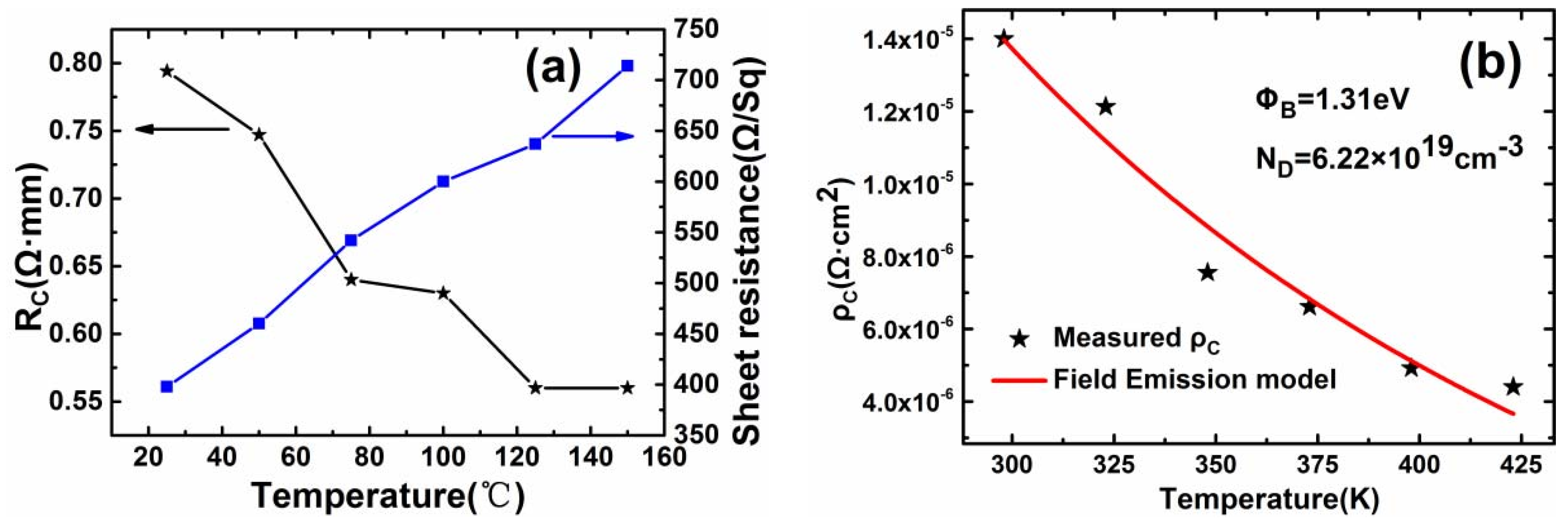
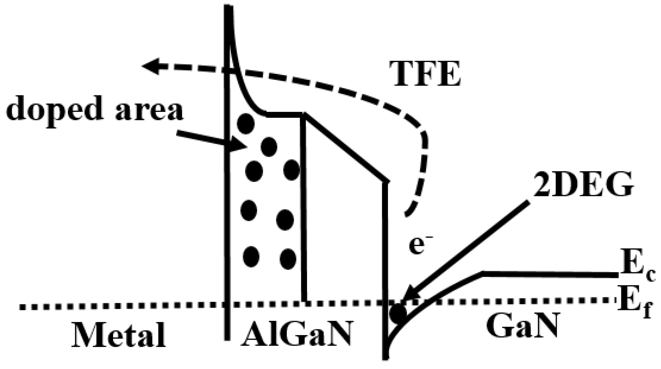
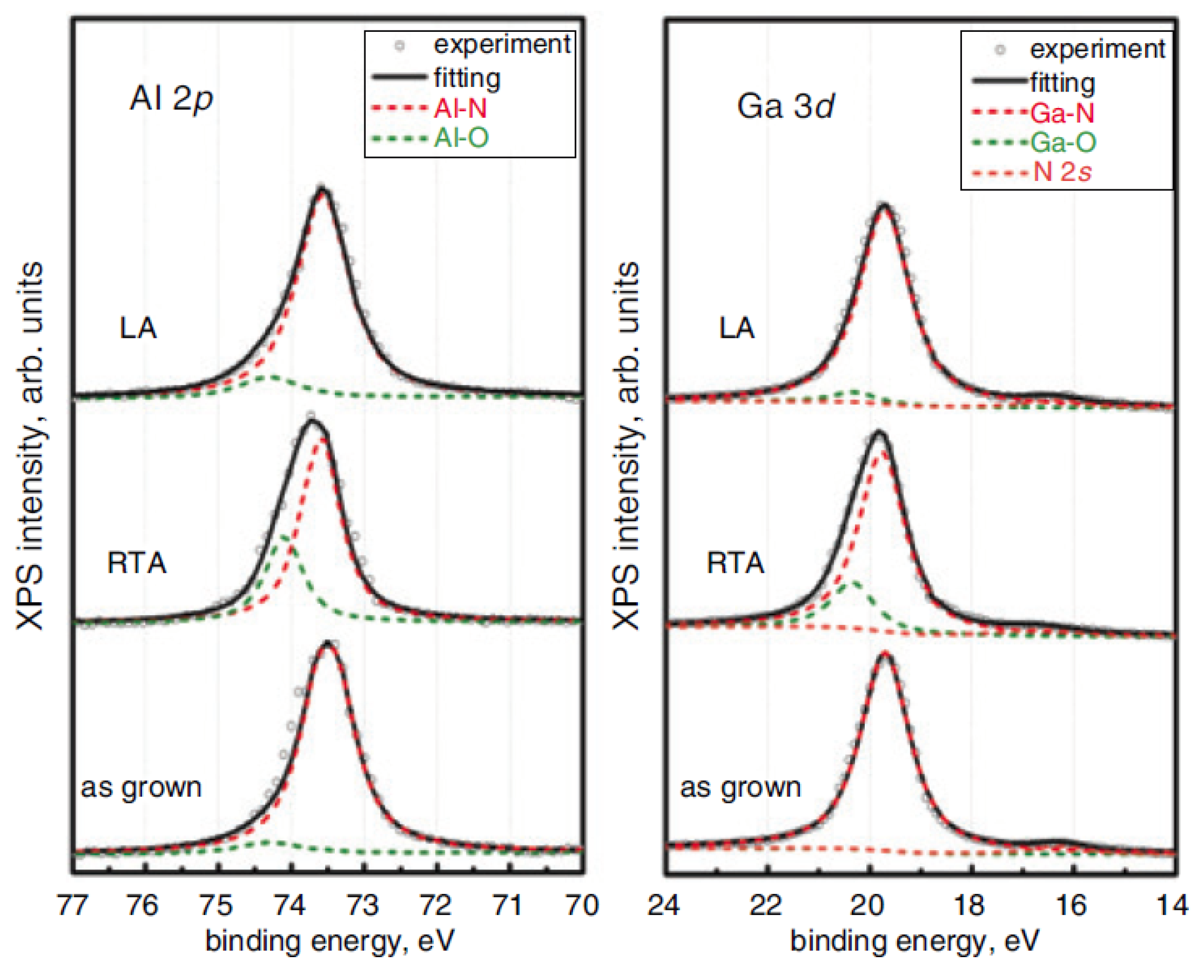
- Zhang, L.Q.; Shi, J.S.; Huang, H.F.; Liu, X.Y.; Zhao, S.X.; Wang, P.F.; Zhang, D.W. Low-temperature ohmic contact formation in GaN high electron mobility transistors using microwave annealing. IEEE Electron Device Lett. 2015, 36, 896–898. [Google Scholar] [CrossRef]
- Zhang, L.Q.; Liu, Z.; Zhao, S.X.; Lin, M.Z.; Wang, P.F. Low-Temperature Ohmic Contact Formation in AlN/GaN HEMT Using Microwave Annealing. IEEE Trans. Electron Devices 2017, 64, 1385–1389. [Google Scholar] [CrossRef]
- Liu, Z.; Zhang, L.Q.; Shi, J.S.; Liu, X.Y.; Zhao, S.X.; Huang, H.F.; Wang, P.F. Mechanism of ohmic contact formation in AlGaN/GaN high electron mobility transistors using microwave annealing. In Proceedings of the 2016 13th IEEE International Conference on Solid-State and Integrated Circuit Technology (ICSICT), Hangzhou, China, 25–28 October 2016; pp. 1050–1052. [Google Scholar]
- Chou, L.I.; Peng, L.Y.; Wang, H.C.; Chiu, H.C.; Wang, H.T.; Chiang, D.L.; Chyi, J.I. InAlN/GaN HEMT using microwave annealing for low temperature ohmic contact formation. In Proceedings of the 2017 IEEE Compound Semiconductor Integrated Circuit Symposium (CSICS), Miami, FL, USA, 22–25 October 2017; pp. 1–3. [Google Scholar]
- Tzou, A.J.; Hsieh, D.H.; Chen, S.H.; Li, Z.Y.; Chang, C.Y.; Kuo, H.C. Non-thermal alloyed ohmic contact process of GaN-based HEMTs by pulsed laser annealing. Semicond. Sci. Technol. 2016, 31, 055003. [Google Scholar] [CrossRef] [Green Version]
- Ferreyra, R.A.; Suzuki, A.; Kazumoto, T.; Ueda, D. n++ GaN regrowth technique using pico-second laser ablation to form non-alloy ohmic contacts. IEEE Electron Device Lett. 2017, 38, 1079–1081. [Google Scholar] [CrossRef]
- Hou, M.; Xie, G.; Sheng, K. Improved device performance in AlGaN/GaN HEMT by forming ohmic contact with laser annealing. IEEE Electron Device Lett. 2018, 39, 1137–1140. [Google Scholar] [CrossRef]
- Hou, M.; Xie, G.; Sheng, K. Mechanism of Ti/Al/Ni/Au ohmic contacts to AlGaN/GaN heterostructures via laser annealing. Chin. Phys. B 2019, 28, 037302. [Google Scholar] [CrossRef]
- Hou, M.; Xie, G.; Sheng, K. Low surface damage during ohmic contact formation in AlGaN/GaN HEMT by selective laser annealing. Electron. Lett. 2019, 55, 658–660. [Google Scholar] [CrossRef]
- Hou, M.; Xie, G.; Guo, Q.; Sheng, K. Protection of isolated and active regions in AlGaN/GaN HEMTs using selective laser annealing. Chin. Phys. B 2021, 30, 097302. [Google Scholar] [CrossRef]
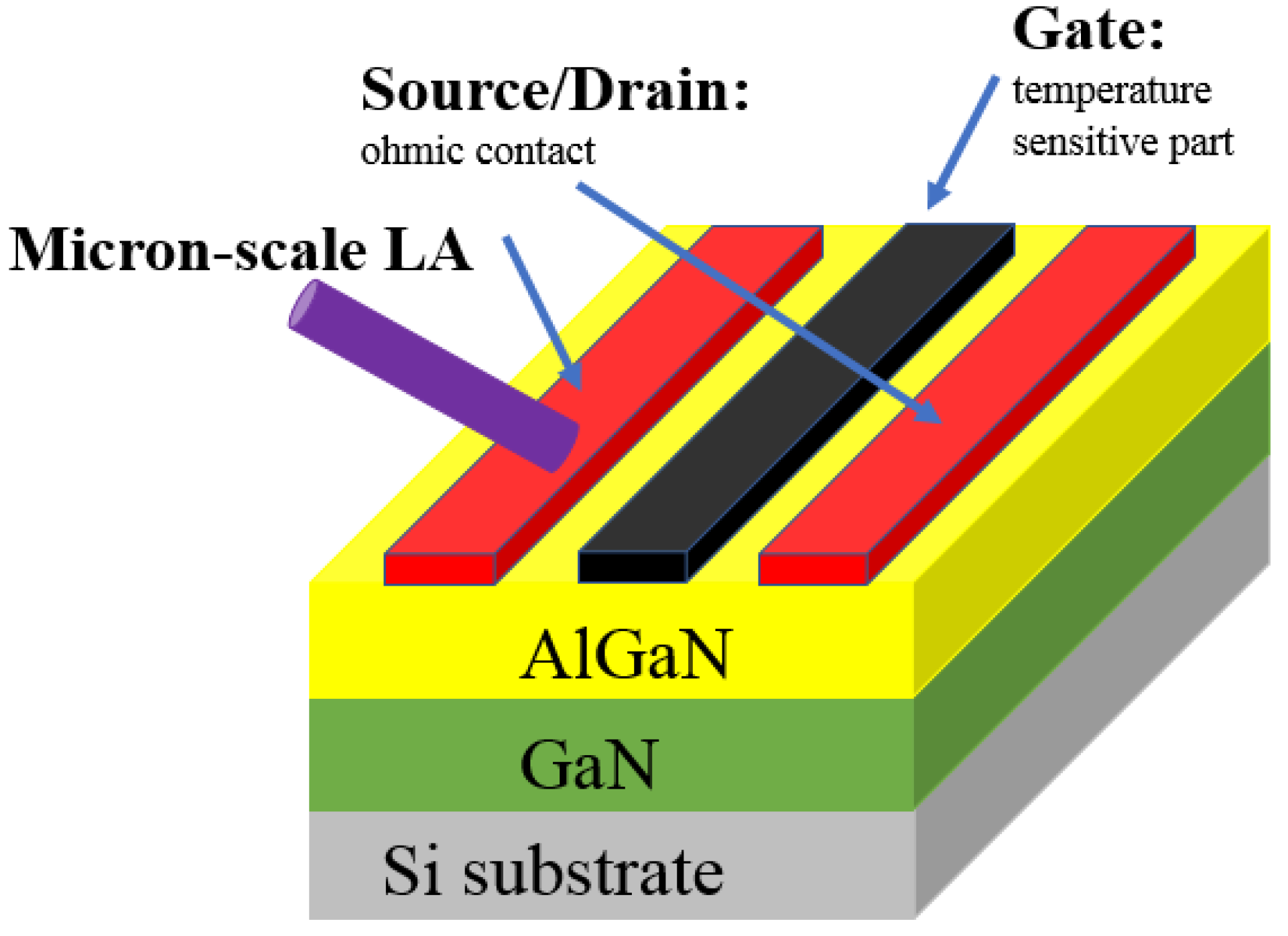
- Liu, Z.; Chen, D.; Wan, L.; Li, G. Micron-scale annealing for ohmic contact formation applied in GaN HEMT gate-first technology. IEEE Electron Device Lett. 2018, 39, 1896–1899. [Google Scholar] [CrossRef]


| Metal | Wm (eV) | ρc (×10−6 Ω/cm2) | ΦB (eV) | Refs. |
|---|---|---|---|---|
| Al | 4.28 | 8 | 0.8 | [38,45] |
| Ti | 4.33 | 3 | 0.58 | [38,39,40,41,43] |
| Au | 5.1 | 2.35 | 0.9 | [38,43,44] |
| Ni | 5.15 | 6.99 | 1.4 | [38,41,44] |
| Mo | 4.6 | 5.3 | 0.81 | [42] |
| Pd | 5.12 | 9.78 | 1.9 | [38,46] |
| Pt | 5.65 | 11 | 1.6 | [38,41] |
| Cr | 4.5 | 11.8 | 0.39 | [41] |
| Au-Free Schemes | RC (Ω·mm) | Idmax (mA/mm) | RON (Ω·mm) | Specific On-State Resistivity (mΩ/cm2) | Gm (mS/mm) | Root-Mean-Square (RMS) Surface Roughness (nm) | Ref. |
|---|---|---|---|---|---|---|---|
| Ti/Al/W | 0.358 | 422 | 9.7 | / | 73.2 | / | [33] |
| Ta/Al/Ta | 0.2 | 263 | 41.3 | / | 55 | / | [69] |
| Ti/Al/Ti/TiN | 0.21 | / | / | / | / | / | [71] |
| Ta/Si/Ti/Al/Ni/Ta | 0.24 | 830 | / | / | 250 | / | [72] |
| Ti/Al/Ni/Pt | 0.6 | 700 | / | 0.77 | 140 | 4.6 | [73] |
| Ti/Al/TiN | 0.62 | / | / | / | / | / | [74] |
| Ti/Al/NiV | 0.13 | 210 | / | 2.3 | 60 | / | [76] |
| Ti/Al/Ti/W | 0.41 | 350 | / | / | / | 7 | [78] |
| TixAly | 0.063 | / | / | / | / | / | [79] |
| Ti/Al/Ni/Ti | / | 400 | 15.6 | 6.39 | / | 7.9 | [80] |
| Methods | Peak Temperature (°C) | RC (Ω·mm) | RMS (nm) |
|---|---|---|---|
| MWA, 3500 W, 20 min | 579.6 | 1.16 | 37.7 |
| MWA, 4200 W, 5 min | 579.6 | 4.57 | 37.5 |
| MWA, 4200 W,10 min | 594 | 4.02 | 35.8 |
| MWA, 4200 W, 15 min | 597.6 | 1.44 | 49.6 |
| MWA, 4200 W, 20 min | 597.6 | 0.6 | 63.5 |
| RTA, 840 °C, 35 s | 840 | 0.4 | 101 |
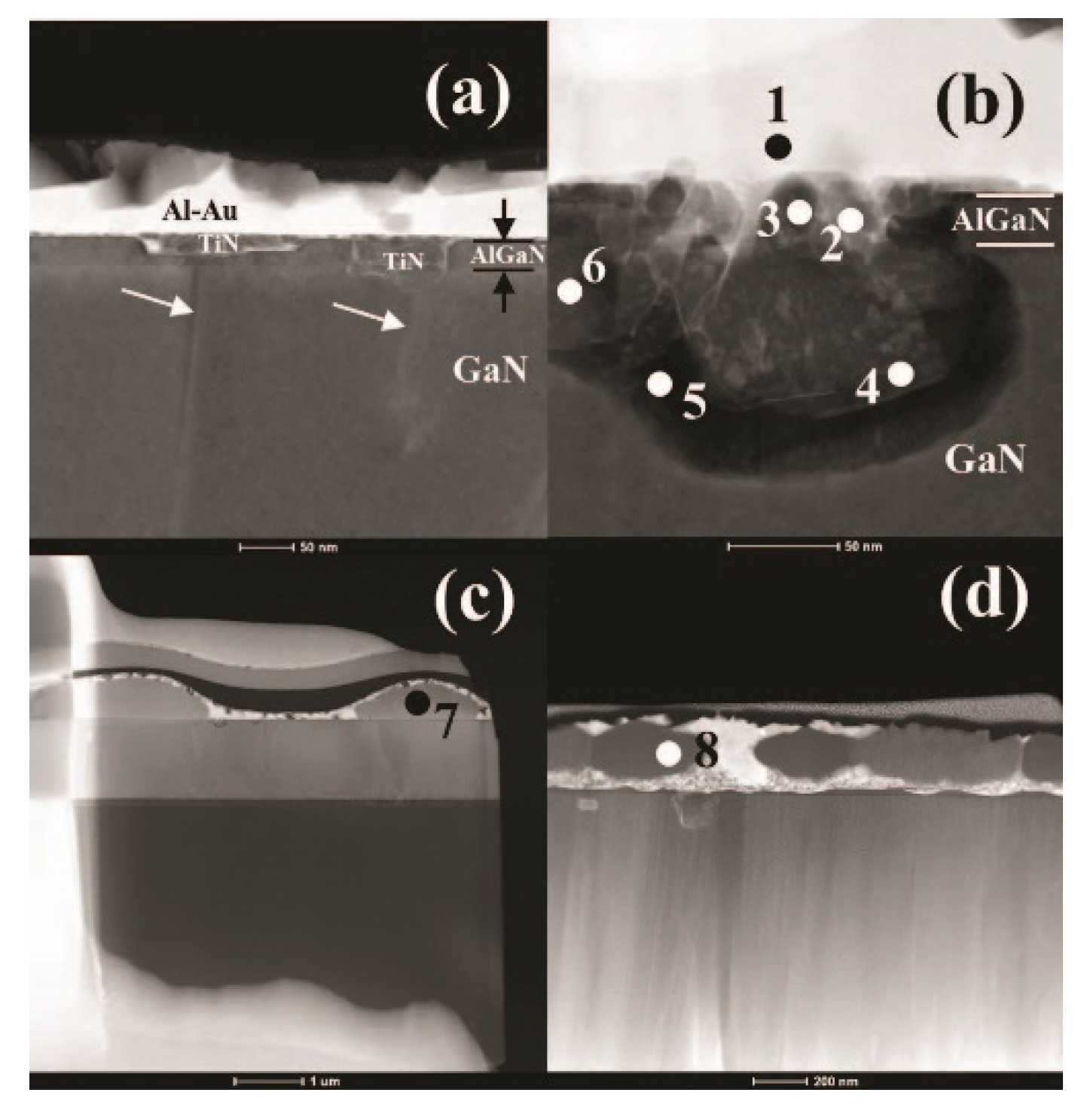
| N | Al | Ti | Ni | Ga | Au | |
|---|---|---|---|---|---|---|
| 1 | 26.37 | 2.76 | 70.87 | |||
| 2 | 9.95 | 57.37 | 7.10 | 3.42 | 22.16 | |
| 3 | 89.30 | 2.47 | 8.23 | |||
| 4 | 8.96 | 83.24 | 1.63 | 6.16 | ||
| 5 | 97.81 | 1.59 | 0.60 | |||
| 6 | 19.53 | 20.27 | 23.75 | 35.20 | 1.26 | |
| 7 | 48.77 | 45.49 | 5.75 | |||
| 8 | 51.35 | 48.65 |
| Material | Methods | Temperature (°C) | RC (Ω·mm) | ρc (×10−5Ω/cm2) | RMS (nm) | Idmax (mA/mm) | RON (Ω·mm) | Gm (mS/mm) |
|---|---|---|---|---|---|---|---|---|
| AlGaN/GaN | MWA | 579.6 | 0.6 | / | 63.5 | 850 | / | / |
| AlGaN/GaN | RTA | 840 | 0.4 | / | 101 | 800 | / | / |
| AlN/GaN | MWA | 572.4 | 0.65 | / | 29.3 | 1400 | / | 270 |
| AlN/GaN | RTA | 750 | 0.4 | / | 56.5 | 1320 | / | 267 |
| InAlN/GaN | MWA | / | / | 4.29 | 6.79 | / | 4.9 | / |
| InAlN/GaN | RTA | 875 | / | 4.02 | 115 | / | 6.1 | / |
Publisher’s Note: MDPI stays neutral with regard to jurisdictional claims in published maps and institutional affiliations. |
© 2022 by the authors. Licensee MDPI, Basel, Switzerland. This article is an open access article distributed under the terms and conditions of the Creative Commons Attribution (CC BY) license (https://creativecommons.org/licenses/by/4.0/).
Share and Cite
Zhang, L.-Q.; Wu, X.-L.; Miao, W.-Q.; Wu, Z.-Y.; Xing, Q.; Wang, P.-F. Process of Au-Free Source/Drain Ohmic Contact to AlGaN/GaN HEMT. Crystals 2022, 12, 826. https://doi.org/10.3390/cryst12060826
Zhang L-Q, Wu X-L, Miao W-Q, Wu Z-Y, Xing Q, Wang P-F. Process of Au-Free Source/Drain Ohmic Contact to AlGaN/GaN HEMT. Crystals. 2022; 12(6):826. https://doi.org/10.3390/cryst12060826
Chicago/Turabian StyleZhang, Lin-Qing, Xiao-Li Wu, Wan-Qing Miao, Zhi-Yan Wu, Qian Xing, and Peng-Fei Wang. 2022. "Process of Au-Free Source/Drain Ohmic Contact to AlGaN/GaN HEMT" Crystals 12, no. 6: 826. https://doi.org/10.3390/cryst12060826