
Simulation of Amorphous Silicon Carbide Photonic Crystal Absorption Layer for Solar Cells


College of Physics, Qingdao University, Qingdao 266071, China
*
Authors to whom correspondence should be addressed.
Crystals 2022, 12(5), 665; https://doi.org/10.3390/cryst12050665
Submission received: 28 April 2022
/
Revised: 4 May 2022
/
Accepted: 4 May 2022
/
Published: 5 May 2022
(This article belongs to the Special Issue Advances of Perovskite Solar Cells)
Abstract
:In this work, the amorphous silicon carbide (a-SiC) with low cost and high extinction coefficient was used as the light absorption layer of solar cells, and the photonic crystal (PC) structure and defect structure were introduced. By optimizing the scatterer shape, structural parameters and defect types of photonic crystal, the absorption efficiency of the light absorption layer was further improved. The results show that the photonic crystal absorption layer with vacancy line defect is better than the perfect photonic crystal absorption layer. Meanwhile, the absorption efficiency of the photonic crystal absorption layer significantly improves in the case that the scatterer is an elliptical cylindrical air hole scatterer. When the incident light is in the wavelength range of 0.30~0.80 μm and the absorption layer height is 0.60 μm, the absorption efficiency of the absorption layer can reach 95.60%. Compared with the absorption layer without photonic crystal structure, the absorption layer is increased by 43.24%. At the same time, the absorption layer has little dependence on the incidence angle of sunlight. When the incidence angle is 65°, the absorption efficiency is still higher than 80%.
1. Introduction
In recent years, the photovoltaic solar cells have rapidly developed [1,2,3,4], but there are following two factors that restrict their large-scale commercial production: the low absorption efficiency of the absorber layer, and the high production cost [5,6,7,8]. Among commercial solar cell products, the crystalline silicon solar cells are the earliest and most mature solar cells [9], but the highest photoelectric conversion efficiency of crystalline silicon solar cells is only 26.7% ± 0.5% [10]. Moreover, the thickness of the silicon layer in crystalline silicon solar cells is several hundred microns, and the cost of silicon materials is too high. Furthermore, a large number of by-products of silicon tetrachloride would be produced in the production process, leading to the potential hazard to safety [11,12]. The later copper indium gallium selenium thin-film solar cell has photoelectric conversion efficiency up to 22.6% at present [13]. However, the battery contains rare elements of indium and gallium, leading to the increasing production cost, and poor stability [14], which bring out the inferior battery performance. Therefore, the design and development of low-cost and high-efficiency photovoltaic solar cells has become a hot research topic.
The amorphous SiC is a kind of semiconductor material with low price and excellent optical performance. Derst [15] has found that the optical absorption of amorphous SiC in the photon energy region below the bandgap is much higher than that of its crystalline phase. Rahul Pandey [16] designed hydrogenated amorphous SiC (a-SiCX: H) to contact silicon solar cells after passivation, taking into account the photon effect and electronic effects. Such strategy can achieve efficient and reliable solar cells. In this work, the modified amorphous SiC is adopted, and the optical bandgap of the material is regulated by controlling the stoichiometric ratio of Si and C to realize the application of SiC in solar cells. The change in Si/C ratio has an impact on the chemical bonding inside the atoms, the refractive index of the film, the absorption coefficient, and so on. Liu et al. [17] controlled the size and distribution of silicon quantum dots in SiC film by changing the Si/C ratio and B doping concentration, in order to realize the control of photoelectric characteristics. Furthermore, Han et al. [18] have experimentally proved that the addition of microcrystalline silicon was helpful to reduce the attenuation effect of amorphous silicon, leading to the improvement of photocell stability. In addition, amorphous SiC can also improve the solar energy absorption efficiency and photoelectric conversion efficiency by changing the ratio of Si/C. Therefore, amorphous SiC materials have broad application prospects in the field of solar cells. At the same time, in order to further improve the light absorption efficiency of solar cells, the photonic crystal structure is introduced into the cell in this work. The photonic crystal structure is an artificial crystal structure, which is formed by periodically arranging two or more materials with different dielectric constants in space. Its main characteristic is the existence of photonic bandgap (PBG) in one or more directions [19]. The incident light within the bandgap cannot transmit inside the photonic crystal, thereby enhancing the interaction between the incident light and the material [20]. When the electromagnetic wave travels in a photonic crystal, it can be modulated by the presence of Bragg scattering, along with a band structure formation for electromagnetic wave energy. In this way, the generally known “photon bandgap” appears. The photon with energy in the range of the photonic bandgap cannot enter the crystal, which can achieve the control of the photon movement. The application of photonic crystal structure in the absorption layer of solar cells is becoming more and more extensive. Through utilizing the characteristic of photon bandgap, the shape and arrangement of the scattering elements are optimized to increase the propagation route of sunlight in photonic crystals and improve the absorption efficiency of solar cells [21]. Our research group has previously designed an ultra-thin gallium arsenide (GaAs) photonic crystal absorption layer with a thickness of 200 nm, which significantly improves the light absorption efficiency [22]. Ottermusch [23] designed a photonic crystal absorption layer and arranged hemispherical copper indium selenide (CuInSe2) scatterers on the absorption layer, which greatly improved the optical absorption rate [24].
The introduction of a defect structure in the perfect photonic crystal structure can change the original periodic structure [25]. The slow light [26] effect obtained by introducing a series of point defects or line defects greatly improves the absorbance of the absorption layer, thereby optimizing the absorption layer structure with higher photoelectric performance [27,28,29,30,31,32]. Therefore, the absorption layer with a photonic crystal structure is designed in this work. Furthermore, the parameters of the scatterer are analyzed and optimized. Finally, the optimal absorption layer structure is obtained.
In this paper, in order to overcome the low absorption efficiency and high production cost faced by the solar cells, photonic crystals are introduced into the solar absorption layer. Firstly, by optimizing the structural parameters of photonic crystals, the greatly improved light absorption efficiency is obtained for the absorption layer. In the following section, the different parameters of cylindrical, elliptical cylindrical, and elliptical tube scattering elements are simulated, and the optimal design of the solar cell absorption layer is obtained. Then, the defect structure [33] is further introduced and its influence on absorption efficiency is discussed. At last, the full analysis and summary are carried out, and the perspective is proposed for the future development direction.
The relevant schematic process of the simulation experiments in this work is shown in Figure 1.
2. The Design of the Absorption Layer
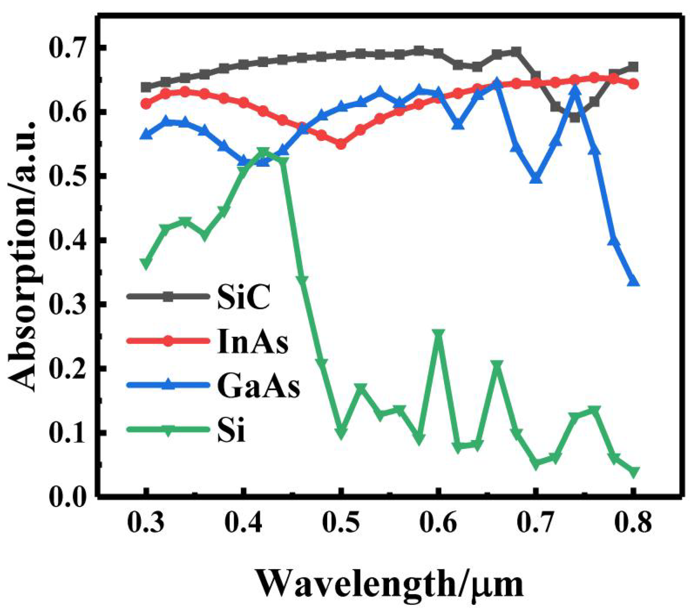
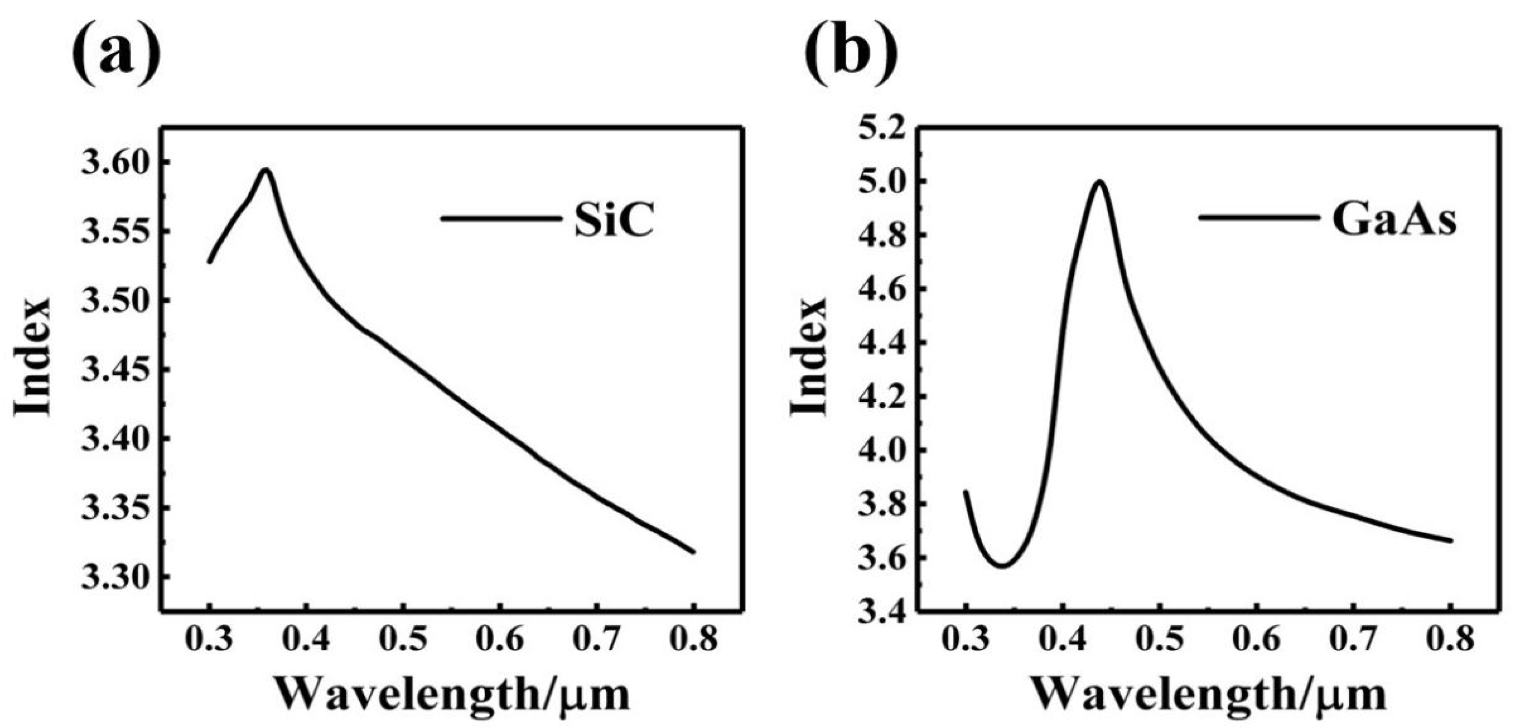
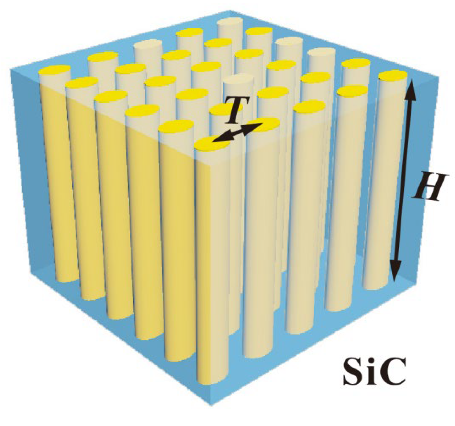
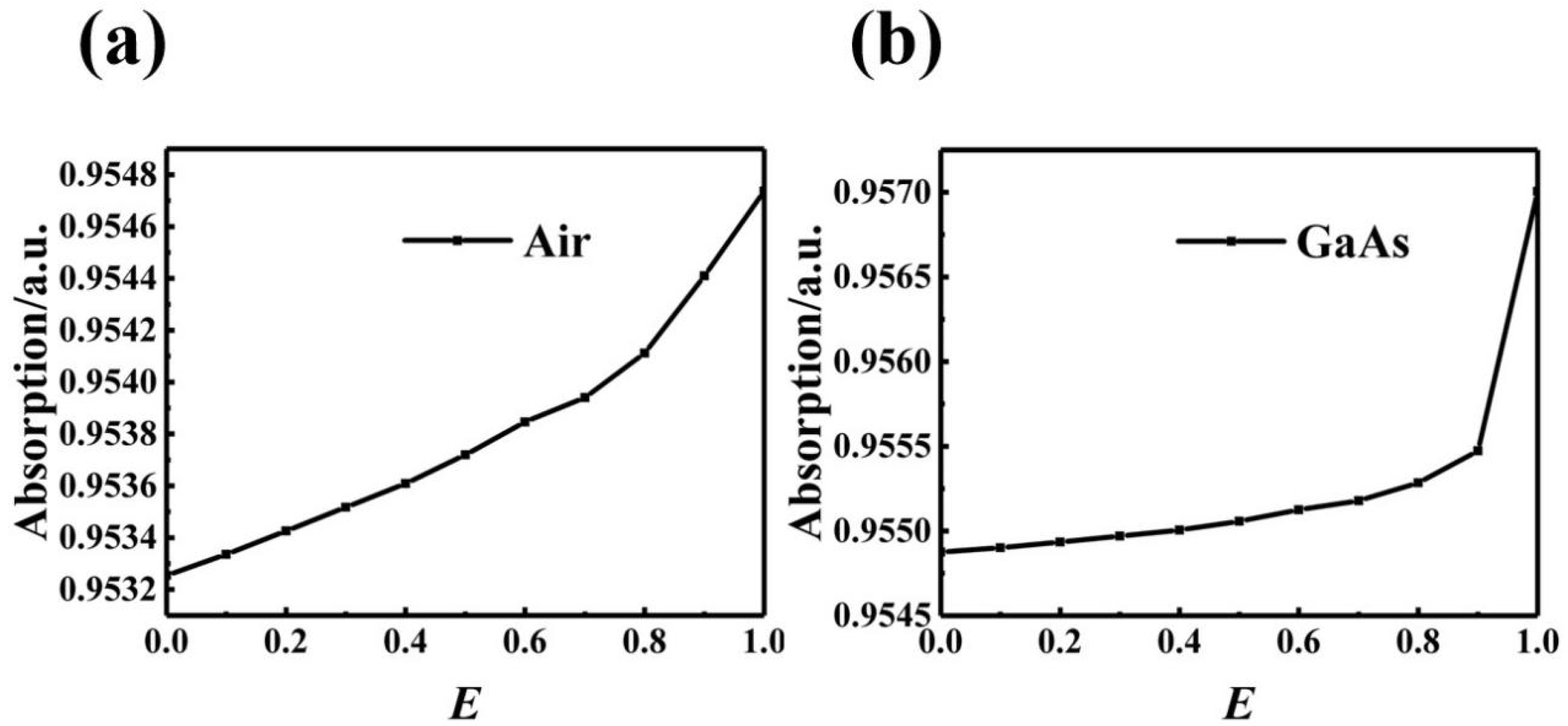
Since the solar energy radiation mainly concentrates in the visible light region and reaches the strongest value at the wavelength of 0.55 μm, the incident light wavelength range within 0.55 ± 0.25 μm is selected. Figure 2 shows the absorption of incident light with a wavelength of 0.3~0.8 μm using various common semiconductor materials. It can be found that the absorption efficiency of amorphous SiC material in this wavelength range is relatively high and stable. Therefore, the amorphous SiC is an ideal choice for the light absorption layer. The cost-effective GaAs is selected as the scattering element in the photonic crystal structure, which is designed into a cylindrical/elliptic cylindrical/elliptical tube type and arranged in the light absorption layer in a tetragonal lattice manner. Figure 3a,b is the refractive index distributions of amorphous SiC material and GaAs, respectively. Figure 4 is the schematic diagram of a-SiC absorption layer with the photonic crystal structure.
3. The Simulation of the Absorption Layer
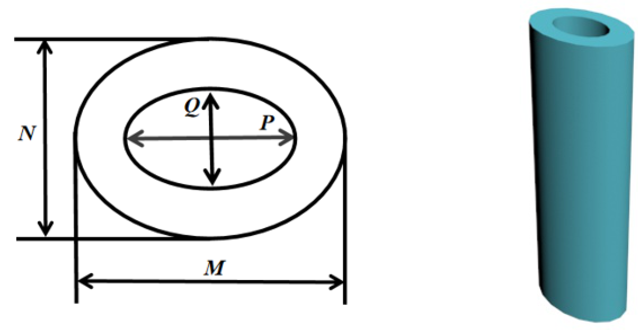
In this work, the Rigorous Coupled Wave method Analysis [34] (RCWA) is used to simulate the absorption layer of the amorphous SiC photonic crystal structure. The parameters related to absorption efficiency including scatterer height H, lattice constant T, cylindrical scattering element diameter D, elliptical cylindrical scattering element long-wheelbase A, and short wheelbase B, long wheelbase of the inner ring of elliptic ring scattering element P, inner ring short wheelbase Q and outer ring long-wheelbase M, outer ring short wheelbase N were optimized to determine the optimal absorption layer structure.
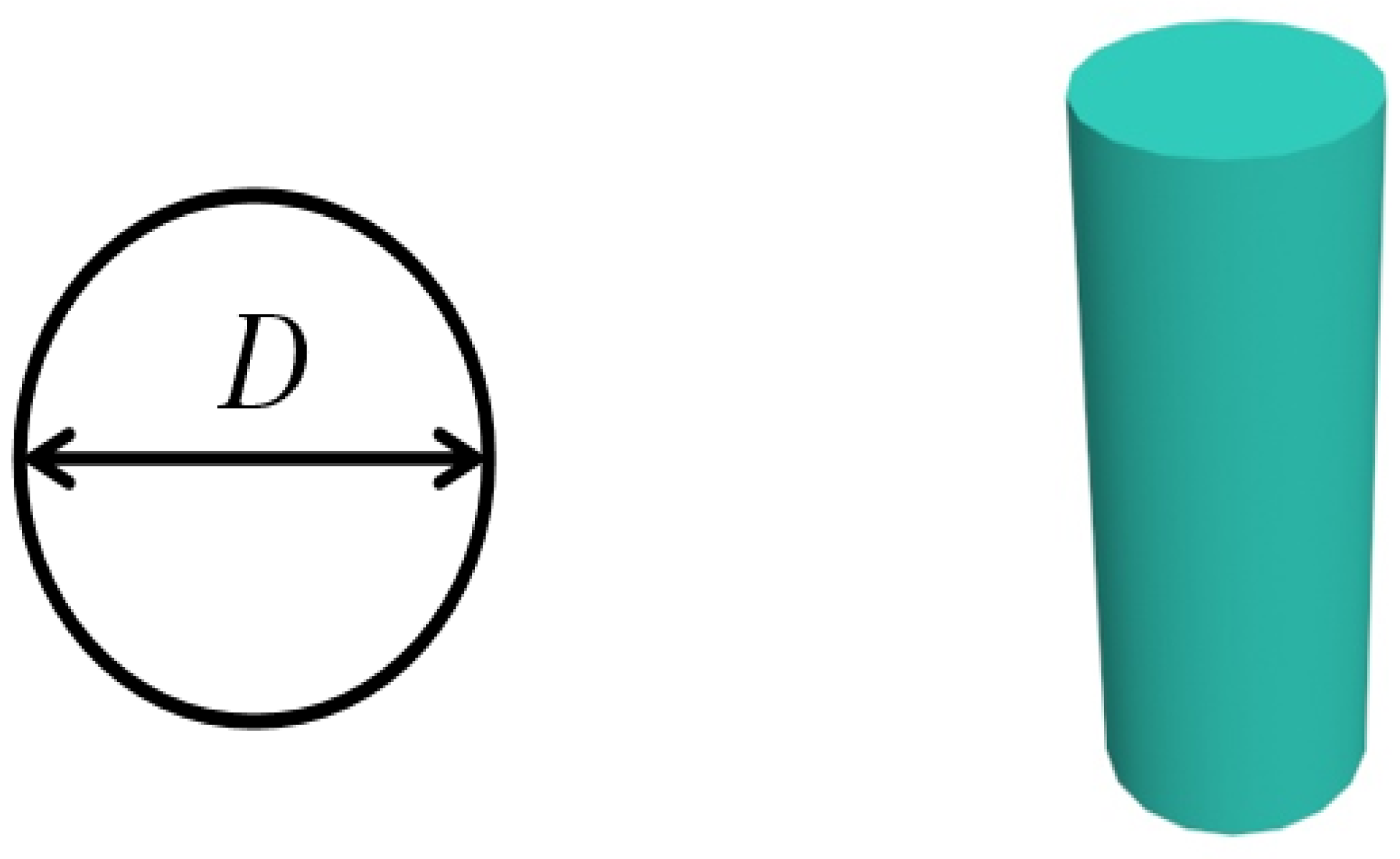
3.1. Cylindrical Scattering Element
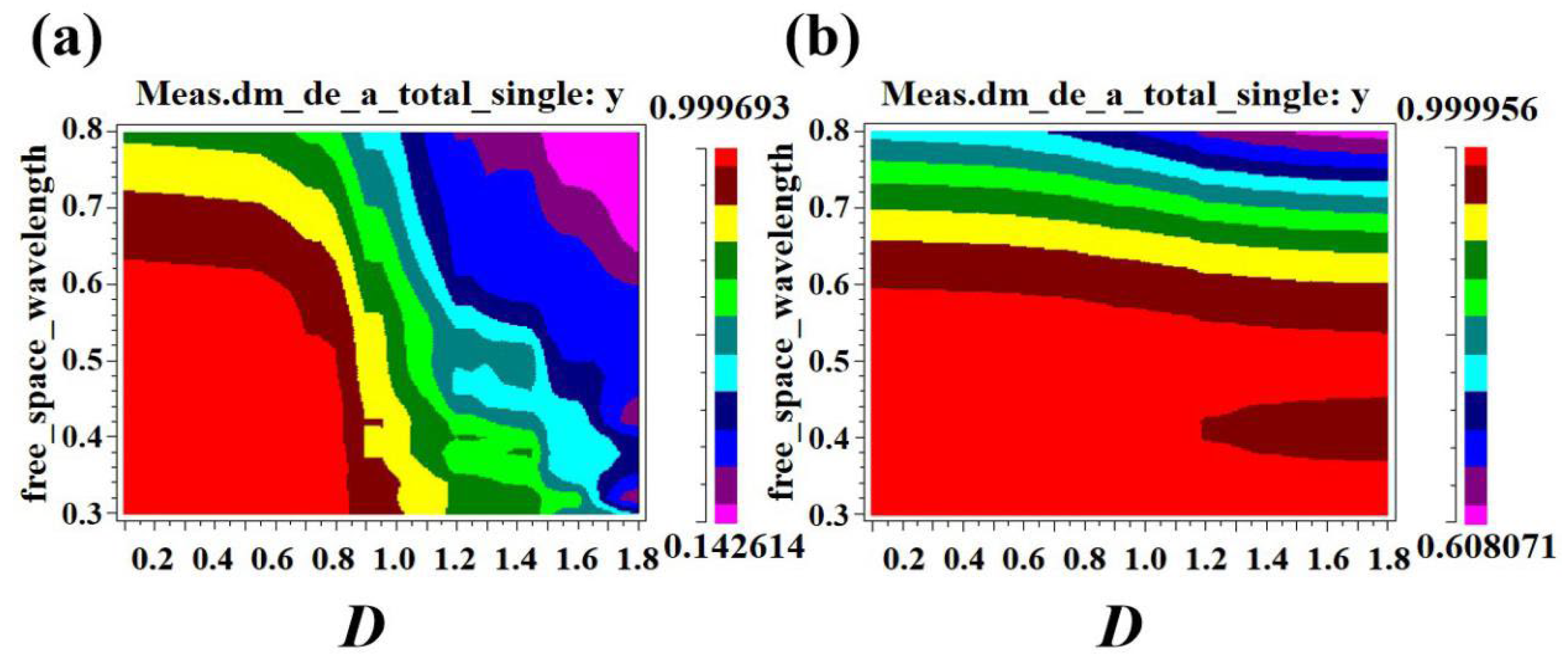
Figure 5 is the schematic diagram of cylindrical scattering element. When the scattering element is cylindrical, the simulation result of absorption efficiency based on the diameter D is shown in Figure 6. Figure 6a shows the dependence of the absorption efficiency of the absorption layer with air-hole scattering elements on the diameter D. Figure 6b shows the absorption efficiency of the absorption layer with GaAs columnar scattering elements as a function of diameter D.
As shown in Figure 6a,b, when the D is higher than 0.2 μm, the absorption efficiency of two-type scattering elements decreases with the increase of diameter D. The contacting area between incident light and photonic crystal absorption layer decreases with the increasing D in terms of the air hole scattering element. Furthermore, such interaction also weakens with the increase of D. When D > 1 μm, the interaction is quite small, leading to the sharply decreasing absorption efficiency. In order to further analyze the effect of different D values on the absorption efficiency, the results of Figure 6a,b are plotted in Table 1.
It can be seen from Table 1 that when the D is 0.1 μm, the light absorption layer of two-type scattering elements achieved the maximum absorption efficiency. Therefore, D = 0.1 μm is chosen as the optimal scatterer diameter under this condition.
Secondly, the simulation result of absorption efficiency based on the lattice constant T is shown in Figure 7. Figure 7a shows the dependence of the absorption efficiency of the absorption layer with air-hole scattering elements on lattice constant T. Figure 7b shows the absorption efficiency of the absorption layer with GaAs columnar scattering elements as a function of the lattice constant T.
It can be seen from Figure 7a,b that the absorption efficiency for absorption layers with different scatterer types increases with the increase of lattice constant T. When taking different lattice constants, the absorption efficiency value of the absorption layer is plotted in Table 2.
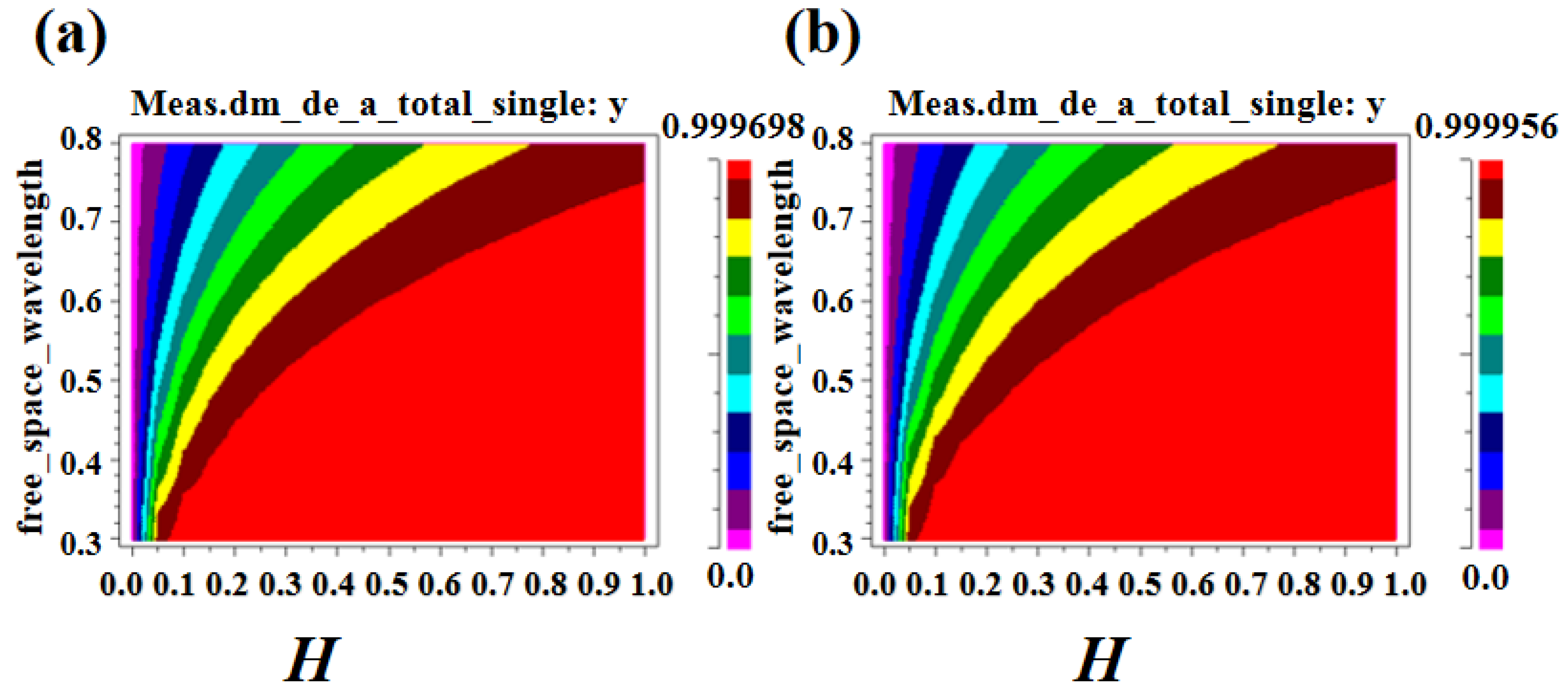
As can be seen from Table 2, the absorption efficiency of the absorption layer initially increases with the increase of T, and then gradually tends to be stable. After T > 1.8 μm, the absorption efficiency is almost unchanged. Therefore, T = 1.8 μm is selected as the optimal value of lattice constant at this time. Finally, the height H is optimized, and the corresponding simulation results are shown in Figure 8. Figure 8a shows the variation of absorption efficiency with height H in the case of air hole scatterers. Figure 8b shows the variation of absorption efficiency with height H in GaAs column scatterers.
It can be seen from Figure 8a,b that the absorption efficiency of the absorption layer with two different scattering element types increases with the increase of H. Similarly, the corresponding absorption efficiency at different H values is plotted in Table 3.
It can be seen from Table 3 that the absorption efficiency increases with the increase of H, but after H > 0.6 μm, the value tends to be stable. At the same time, it is considered that with the increase of height H, the carrier migration distance increases, resulting in the increase of recombination probability and the decrease of photovoltaic conversion efficiency of solar cells. Therefore, H = 0.6 μm is chosen as the optimal value of the scatterer height.
3.2. Elliptic Cylindrical Scattering Element
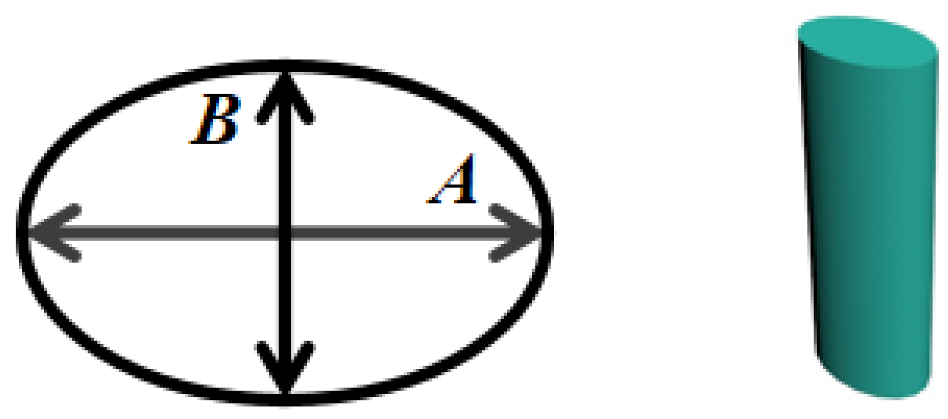
The elliptical cylindrical scattering element is optimized based on the cylindrical scattering element. The lattice constant T is set to be 1.8 μm, while the height H is set to be 0.6 μm. A new parameter E = 1−B/A is defined, where A represents the long-wheelbase of the elliptical cylindrical scattering element, B represents its short wheelbase, and E represents the shape of the elliptic cylindrical scatterer changing with the long and short wheelbase. In this work, the long wheelbase A is fixed to be 0.1 μm, and the short wheelbase B is adjusted by the change of the E. Figure 9 is a schematic diagram of an elliptical cylindrical scattering element. Figure 10a shows the change of the absorption rate of the absorption layer with the parameter E when the elliptical cylindrical scattering element is an air hole. Figure 10b shows the change of the absorptance of the absorption layer with the parameter E when the elliptical cylindrical scattering element is GaAs column.
As shown in Figure 10a,b, the absorption efficiency of the two different scattering element types increases with the increase of E. In this case, the flatter the elliptical cylindrical scattering element is, the higher the absorption efficiency of the absorption layer is obtained. When the E varies, the specific values of absorption efficiency are plotted in Table 4. It can be seen that the absorption efficiency of the absorption layer increases with the increase of E. When the parameter E = 0.5 is selected, the absorption efficiency of the absorption layer is the best. Thus, when A = 0.1 μm and B = 0.05 μm, the absorption efficiency of absorption layer with air hole type scattering element is 95.37%, while the absorption efficiency of absorption layer with GaAs elliptical type scattering element is 95.51%.
3.3. Elliptical Tube Scattering Element
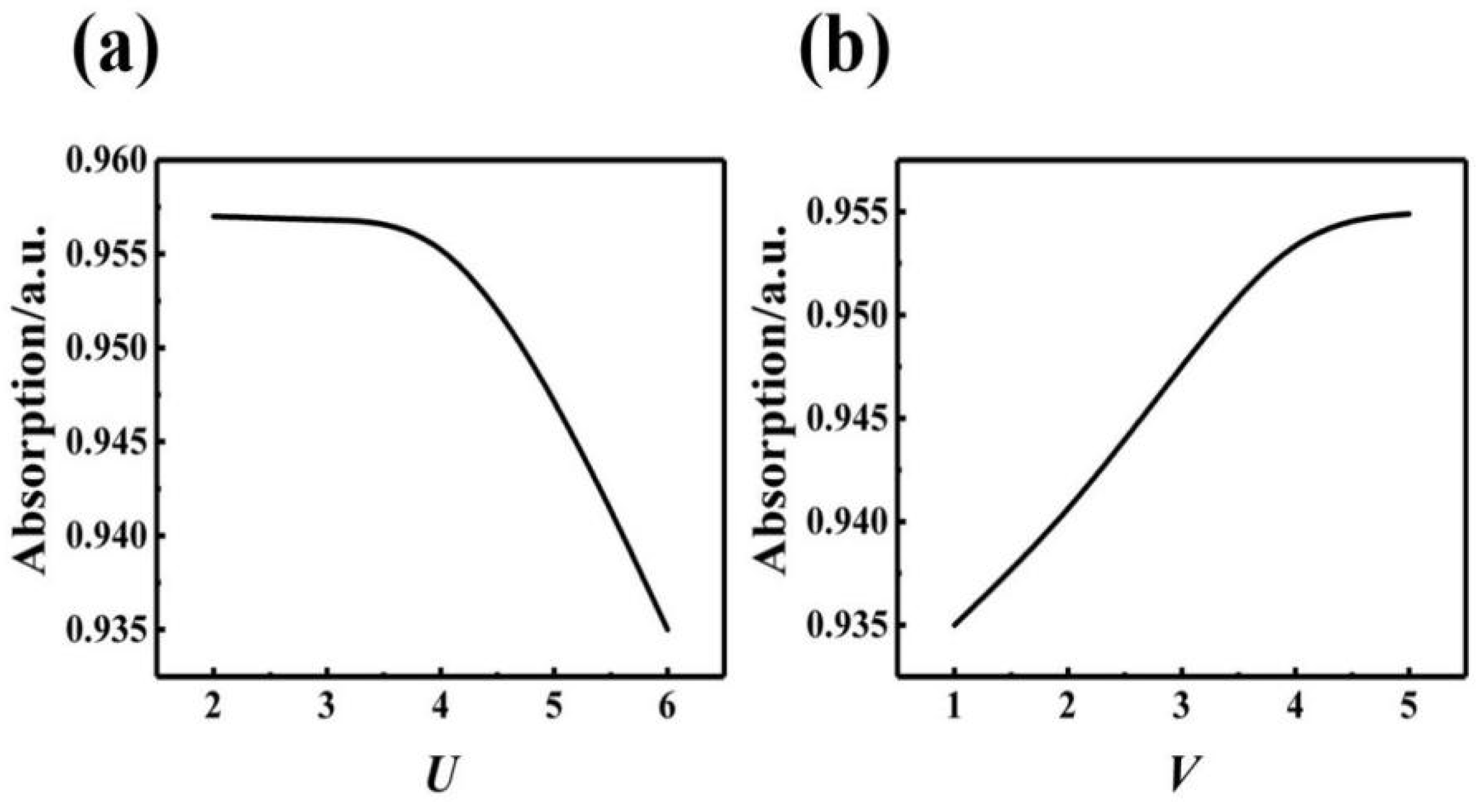
In this section, the air ring scattering elements are arranged in the amorphous SiC absorption layer to simulate the absorption efficiency. The lattice constant T is set to be 1.8 μm, and the height H is set to be 0.6 μm. The parameters U, V is defined, where P represents the long wheelbase of the inner ellipse, B represents the short wheelbase of the inner ring, M represents the long wheelbase of the outer ring, and N represents the short wheelbase of the outer ring. Figure 11 is a schematic diagram of an elliptical tube scattering element. Initially, the parameters of the inner ring were fixed, where the long wheelbase of the inner ring P is set to be 0.1 μm, and the short wheelbase of the inner ring Q is set to be 0.05 μm. By changing the outer ring parameters, the outer ring parameters are multiplied related to the inner ring parameters, i.e., M = U × P, N = U × Q. The variation law of absorption efficiency with parameter U is simulated. Secondly, by fixing the outer ring parameters and changing the inner ring parameters, the inner ring parameters related to P = 0.1 μm, Q = 0.05 μm increases by V times, i.e., P = V × 0.1 μm, Q = V × 0.05 μm. The variation of absorption efficiency with parameter V is simulated. Figure 12a shows the changes of absorption efficiency with U. Figure 12b shows the changes of absorption efficiency with V.
It can be seen from Figure 12a that the absorption efficiency of the absorption layer decreases with the increase of the parameter U, that is, when the inner ring parameters of the elliptical tube scattering element remain unchanged, the absorption efficiency decreases as the outer ring parameters increase. It can be seen from Figure 12b that the absorption efficiency increases with the increase of the parameter V, that is, when the outer ring parameters of the elliptical tube scattering element do not change, the absorption efficiency increases as the inner ring parameters increase. When the parameters of U and V take different values, the specific values of absorption efficiency are plotted in Table 5 and Table 6.
The absorption efficiency of the absorption layer is related to the thickness of the ellipse ring. The thicker the ellipse ring is, the lower the absorption efficiency is obtained, while the thinner the ellipse ring is, the higher the absorption efficiency is obtained. When P = 0.1 μm, Q = 0.05 μm, M = 0.2 μm, and N = 0.1 μm, the absorption efficiency of the absorption layer with air ring scattering element is the highest, which is 95.70%.
3.4. Introduction of Defect State
In consideration of the practicability, the photonic crystal model of the amorphous SiC absorbing layer with elliptic cylindrical scatterers filled with air is used to design a better absorption layer structure. Based on the optimal parameters of the elliptical cylindrical scattering element absorption layer, the simulation analysis is carried out for different types of defect states.
3.4.1. Point Defect
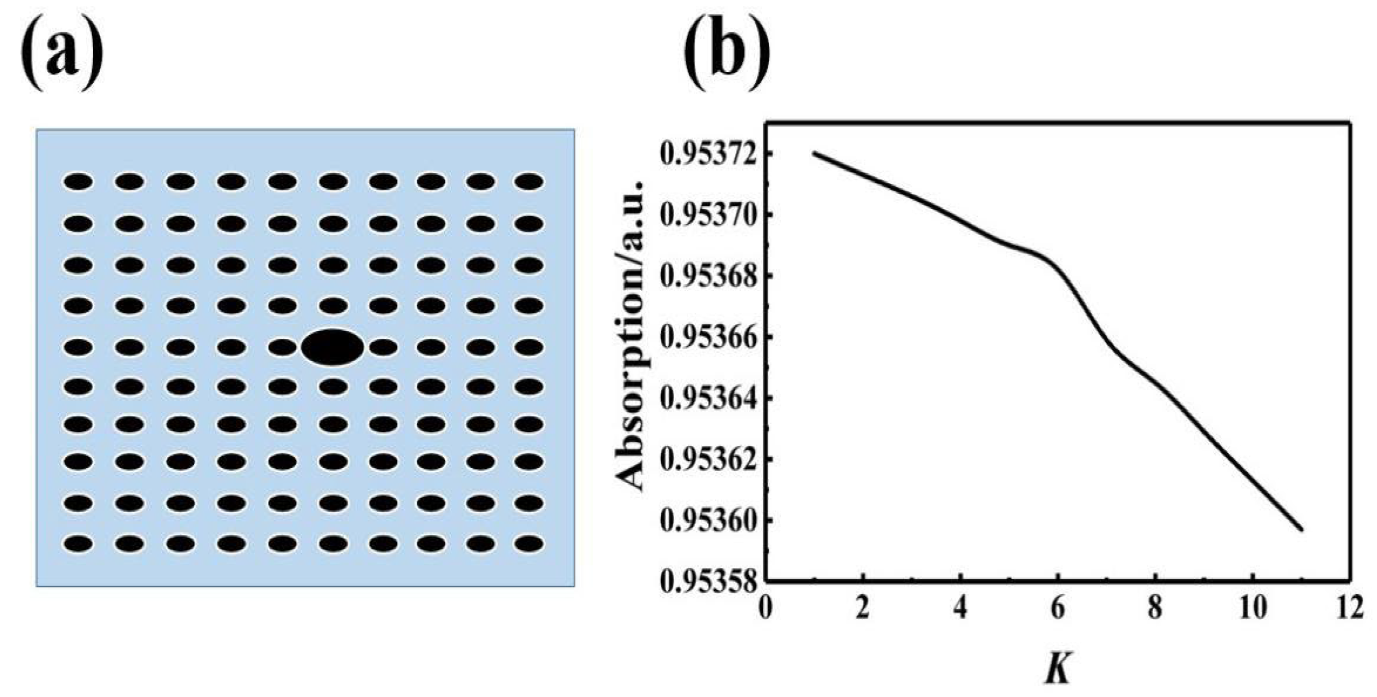
The absorption layer structure of point defect photonic crystal is constructed by changing the size of the scatterer in the middle. The parameter K is defined so that the parameters of the intermediate scattering element change by K times compared with the parameters of other scattering elements. Figure 13a is a diagram of the point defect structure. Figure 13b shows the changes of absorption efficiency of the absorption layer with K.
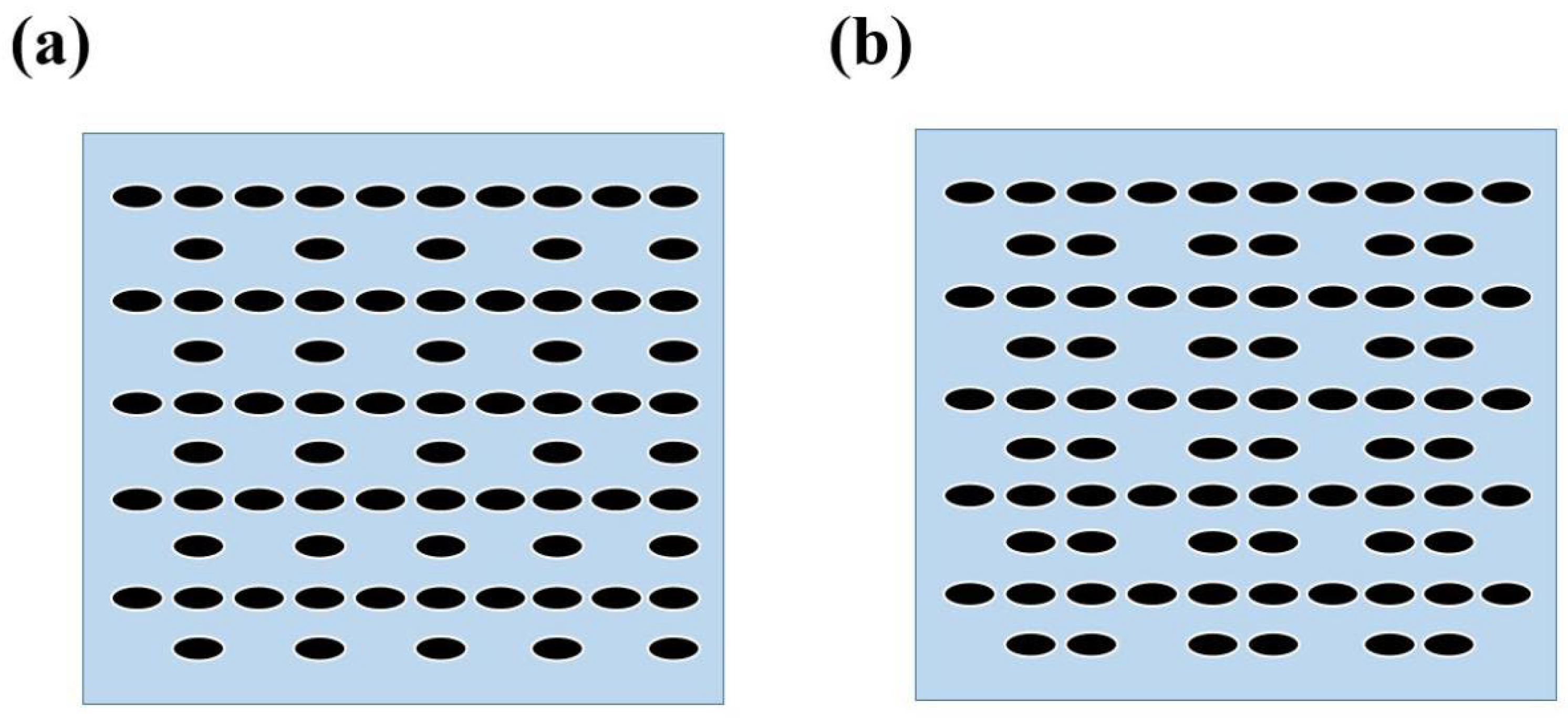
In this work, we mainly study the point defects in which the parameters of the intermediate scattering element change by K times compared with the parameters of other scattering elements. It can be seen from Figure 13b that the absorption layer of photonic crystal with point defects decreases with the increase of K value, that is, the reduction of scatterer parameters A and B will increase the absorption efficiency, and the increase of the scatterer parameters A and B will reduce the absorption efficiency. Due to the limitation of the process precision, it is impossible to carry the simulation in terms of the smaller scattering element parameters. Therefore, it is not considered to change the parameters of the scattering element to optimize the absorption efficiency. The introduction of impurity scattering elements has limited improvement in absorption efficiency and will increase the difficulty of the process. At the same time, it is considered to optimize the structure of absorption layer by introducing vacant site defects into the photonic crystal structure. Figure 14 shows the arrangement modes of two different types of photonic crystals with vacant site defects.
The absorption efficiency of absorption layer with photonic crystal structure shown in Figure 14a is 95.45%, while the absorption efficiency for the structure shown in Figure 14b is 95.43%. The absorption efficiency of the complete photonic crystal absorption layer is 95.37%. It can be seen from the absorption efficiency that the absorption efficiency of the photonic crystal with vacancy point defect is higher than that of the perfect one.
3.4.2. Line Defect
This section focuses on the investigation of line defects and optimizes the structure of the absorption layer by introducing line defects into the photonic crystal. Figure 15 shows the arrangement of two different types of photonic crystals containing vacant bit line defects.
Through simulation calculation, it can be found that the absorption efficiency of the absorption layer with photonic crystal arrangement shown in Figure 15a is 95.43%, while the value of the absorption layer with photonic crystal arrangement shown in Figure 15b is 95.60%, which is also higher than that of the perfect photonic crystal absorption layer.
4. Result Analysis and Discussion
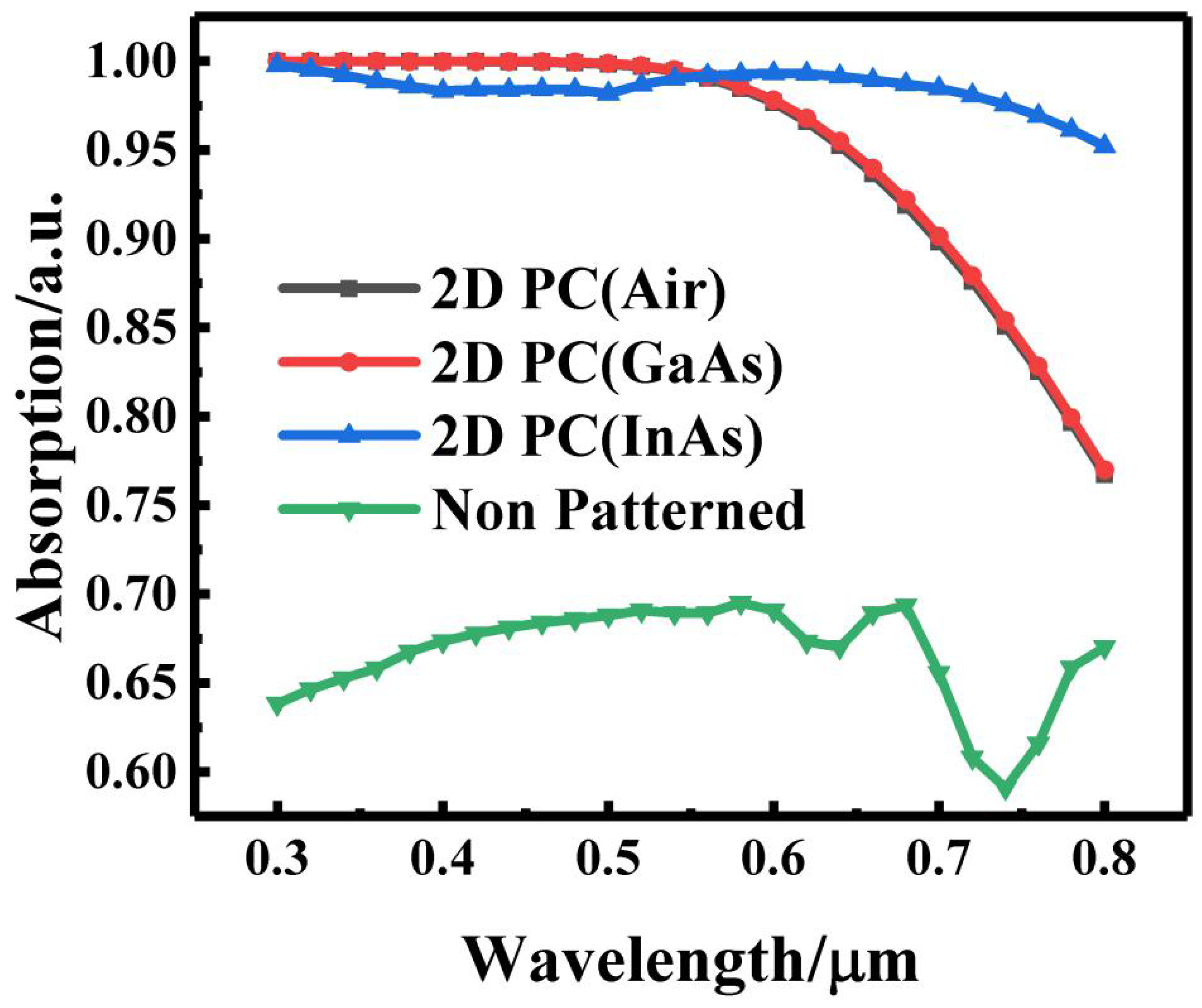
Firstly, the photonic crystal structure in the absorption layer is adopted, which can greatly improve the light absorption efficiency of the absorption layer. In the amorphous SiC absorption layer, the absorption efficiency of the elliptical cylindrical scattering element absorption layer is slightly higher than that of the cylindrical scattering element absorption layer. In addition, the absorption efficiency of the photonic crystal structure absorption layer with indium arsenide as the scattering element material is further simulated. Figure 16 shows the absorption of incident light at a wavelength of 0.3~0.8 μm for various absorption layers with different types of scattering elements and absorption layers without the photonic crystal structure. The absorption efficiency of InAs as the scattering element material of absorption layer is the best. However, the price of InAs is higher than that of GaAs, resulting in an increase in the production cost of solar cells. The absorption efficiency of the layer with air hole scatterers is almost the same as that of the layer with GaAs column scatterers. According to the calculation, the absorption efficiency of the absorption layer without photonic crystal structure is only 66.74%, while the value of the air hole scatterer reaches 95.37%, showing an increase of 42.9%. Therefore, the absorption layer of the photonic crystal structure in this case is the optimal absorption layer structure.
Secondly, compared with the cylindrical scattering element, the ring-shaped scattering element has a larger light contact area and wider broadband slow light, which can make the semiconductor material fully absorb light and obtain higher absorption efficiency. The elliptical tube scattering element has better slow light effect and better performance. However, the elliptical tube scattering element requires higher and more complicated manufacturing process. If necessary, this type of scattering element can be considered for the application of solar cells.
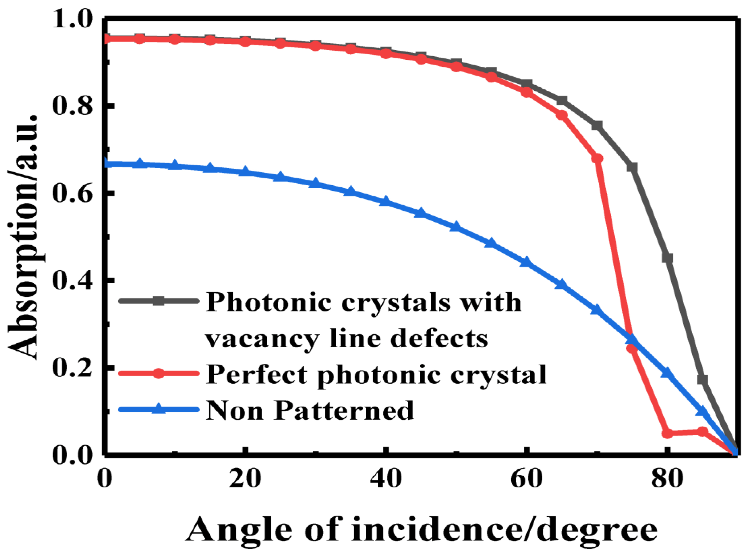
Thirdly, the absorption efficiency of the photonic crystal structure absorption layer equipped with elliptic cylindrical air hole scatterers with vacancy line defects is 95.60%. This is higher than the absorption efficiency of the absorption layer with perfect photonic crystal structure. The absorption efficiency is improved by 43.24% compared with the absorption layer without photonic crystal structure. At the same time, the angle adaptability of the absorption efficiency of the absorption layer under the optimal photonic crystal model is analyzed. Figure 17 shows the absorption efficiency of the absorption layer as a function of incident angle.
On the whole, the absorption efficiency of the absorption layer with photonic crystal arrangement is higher than that without photonic crystal arrangement. When the light is vertically incident, the absorption efficiency of the absorption layer with photonic crystal structure is much higher than that of the absorption layer without photonic crystal structure. It can be seen from Figure 17 that there is a relatively sharp decrease in absorption around 70° to 80°. The effective area of the light decreases with the increase of the incidence angle, leading to the decreasing absorption rate. As for the solar incidence angle and the solar radiation amount, the solar radiation amount tends to be constant in terms of the nearly vertical incidence. Furthermore, the larger the incidence angle is, the greater the rate of change appears, which is similar to the trigonometric function model. When the incident angle is about 75° to 90°, the absorption efficiency of the absorption layer with a perfect photonic crystal structure is slightly lower than that of the absorption layer without the photonic crystal structure. The effect of the photonic crystal structure decreases when the incident light increases almost parallel to the plane of the absorption layer. In addition, the wall thickness of the photonic crystals should be considered, when the light is vertical incident. Under this circumstance, the nearly vertical light will react with the wall, and the effective area of light decreases with the increase of the incident Angle. So, the relative absorption rate will be lower. However, it is not much lower than that without the photonic crystal structure. The total absorption rate of the absorption layer with photonic crystal structures is much more efficient than that without photonic crystals. During installation, the best-fixed inclination mode should be used to reduce maintenance costs and improve absorption efficiency.
The absorption layer with vacancy line defect has the best angle adaptability. In addition, the absorption efficiency of the absorption layer with the incident angle from 0 to 90° is higher than that of the absorption layer with perfect photonic crystal structure and the absorption layer without photonic crystal alignment. When the incident angle is in the range of 0~65°, the absorption efficiency is above 80%. This shows that the reasonable design of the defect type of the photonic crystal can not only improve the absorption efficiency of the absorption layer but also reduce the dependence of the absorption layer on the incident angle of light.
Fourth, the photonic bandgap and slow light effect of photonic crystals with defect structures can provide a powerful light trapping mechanism for thin-film solar cells. Photonic crystals have a unique light dispersion relationship and can be used to control light in various ways. When the light propagates through the photonic crystal, the photon is modulated by the periodic arrangement of the dielectric constant of the photonic crystal. The Bragg scattering occurs when light propagates in the photonic crystal, thus forming the band structure of the photonic crystal. The bandgap between two adjacent photonic band structures is called the photonic bandgap. When the light whose frequency falls in the forbidden band is incident on the photonic crystal, it will be strongly reflected by the photonic crystal, and it can hardly pass through the photonic crystal. The photonic forbidden band can prohibit photons in a certain direction from propagating in the photonic crystal within a certain frequency or wavelength range. The photonic bandgap is usually divided into two categories: complete photon bandgap and incomplete photon bandgap. The complete photonic bandgap is an omni-directional photonic bandgap, that is, photons in a specific frequency or wavelength range cannot propagate or polarize in all directions of the photonic crystal. Only three-dimensional photonic crystals have a complete photonic bandgap, but their practical applicability lags behind two-dimensional photonic crystals. Similarly, the incomplete photonic bandgap means that the photonic bandgap exists only in a specific direction. Changing the lattice parameters of the photonic crystal and the dielectric constant of the dielectric material can change the photonic bandgap of the photonic crystal. The reasonable use of its photonic bandgap can enhance the interaction between light and material, thereby increasing the absorption efficiency of the absorption layer.
In addition, the slow light effect in photonic crystals is mainly formed by the total reflection effect, anti-cross resonance effect, and Bragg resonance effect at the boundary of the Brillouin region provided by the photonic crystal bandgap. Essentially, photonic crystals are produced by the periodic arrangement of two or more materials with a different dielectric constant in space, and the structure will produce strong structural dispersion. When the material has a large enough normal dispersion rate, the group speed of light can be greatly reduced, i.e., the slow light effect. The slow light effect allows the photon to fully interact with the absorption layer material and improve the absorption efficiency of the absorption layer.
Fifthly, in the absorption layer of photonic crystal with vacancy defect structure, the density of photon state at the defect increases significantly. Meanwhile, in the photonic crystal with a defect structure, the photon is localized at the defect position, which is the photon local characteristic of the photonic crystal. Moreover, the defect structure can slow down the propagation speed of light and facilitate the absorption layer to absorb photons, producing more carriers, to increase the absorption efficiency of light and photoelectric conversion efficiency of the absorption layer.
5. Conclusions
In summary, the photonic crystal structure and defect structure of SiC was designed as the absorption layer of solar cells. The scattering elements of different shapes including elliptical tube scattering elements and different defect types were simulated and optimized. Moreover, an amorphous SiC solar cell absorber layer was designed with a two-dimensional photonic crystal structure with vacancy line defects. The photonic bandgap and slow light effect lead to the increased light propagation path and reduced carrier recombination probability. In this way, the light absorption efficiency of the absorption layer is greatly improved. This work provides an important direction for optimizing the absorption layer of new thin-film solar cells by adopting low-cost and high-efficiency photonic crystal structure.
Author Contributions
Methodology, L.Z.; Software, Y.X.; Validation, L.Z. and S.T.; Formal analysis, M.L. and Y.W.; Investigation, S.T.; Resources, Y.X. and S.T.; Writing—original draft preparation, L.Z. and Y.X.; Writing—review and editing, M.L.; Supervision, Y.W.; All authors have read and agreed to the published version of the manuscript.
Funding
This research was funded by the Natural Science Foundation of Shandong Province (Grant No. ZR2020MA084, ZR2019MD016), and the National Natural Science Foundation of China (Grant No. 41976173).
Institutional Review Board Statement
Not applicable.
Informed Consent Statement
Not applicable.
Conflicts of Interest
The authors declare no conflict of interest.
References
- Polman, A.; Knight, M.; Garnett, E.C.; Ehrler, B.; Sinke, W.C. Photovoltaic materials: Present efficiencies and future challenges. Science 2016, 352, aad4424. [Google Scholar] [CrossRef] [PubMed] [Green Version]
- Green, M.A.; Bremner, S. Energy conversion approaches and materials for high-efficiency photovoltaics. Nat. Mater. 2016, 16, 23–34. [Google Scholar] [CrossRef] [PubMed]
- Yeh, N.; Yeh, P. Organic solar cells: Their developments and potentials. Renew. Sustain. Energy Rev. 2013, 21, 421–431. [Google Scholar] [CrossRef]
- Ameri, T.; Khoram, P.; Min, J.; Brabec, C.J. Organic Ternary Solar Cells: A Review. Adv. Mater. 2013, 25, 4245–4266. [Google Scholar] [CrossRef] [PubMed]
- Cao, W.; Xue, J. Recent progress in organic photovoltaics: Device architecture and optical design. Energy Environ. Sci. 2014, 7, 2123–2144. [Google Scholar] [CrossRef]
- Sugathan, V.; John, E.; Sudhakar, K. Recent improvements in dye sensitized solar cells: A review. Renew. Sustain. Energy Rev. 2015, 52, 54–64. [Google Scholar] [CrossRef]
- Carey, G.H.; Abdelhady, A.L.; Ning, Z. Colloidal Quantum Dot Solar Cells. J. Chem. Rev. 2015, 115, 12732–12763. [Google Scholar] [CrossRef]
- Wang, Q.; Xie, Y.; Soltani-Kordshuli, F.; Eslamian, M. Progress in emerging solution-processed thin film solar cells—Part I: Polymer solar cells. Renew. Sustain. Energy Rev. 2015, 56, 347–361. [Google Scholar] [CrossRef]
- Okil, M.; Salem, M.S.; Abdelkader, T.M.; Shaker, A. From Crystalline to Low-cost Silicon-based Solar Cells: A Review. Silicon 2022, 14, 1–17. [Google Scholar] [CrossRef]
- Andreani, L.C.; Bozzola, A.; Kowalczewski, P.; Liscidini, M.; Redorici, L. Silicon solar cells: Toward the efficien-cy limits. Adv. Phys-X 2019, 4, 1548305. [Google Scholar] [CrossRef] [Green Version]
- Munzer, K.; Holdermann, K.; Schlosser, R.; Sterk, S. Thin monocrystalline silicon solar cells. IEEE Trans. Electron Devices 2002, 46, 2055–2061. [Google Scholar] [CrossRef]
- Chang, Y.; Chen, H.Y.; Luo, Q.W.; Ye, Q.H. Preparation of Solar-Grade Polysilicon by Acid Leaching. Adv. Mater. Res. 2010, 160–162, 1297–1300. [Google Scholar] [CrossRef]
- Jackson, P.; Wuerz, R.; Hariskos, D.; Lotter, E.; Witte, W.; Powalla, M. Cover Picture: Effects of heavy alkali elements in Cu(In,Ga)Se2 solar cells with efficiencies up to 22.6% (Phys. Status Solidi RRL 8/2016). Phys. Status Solidi Rapid Res. Lett. 2016, 10, 201670747. [Google Scholar] [CrossRef]
- Tdl, A.; Aue, B. A review of thin film solar cell technologies and challenges. Renew. Sustain. Energy Rev. 2017, 70, 1286–1297. [Google Scholar]
- Derst, G.; Wilbertz, C.; Bhatia, K.L.; Krätschmer, W.; Kalbitzer, S. Optical properties of SiC for crystal-line/amorphous pattern fabrication. Appl. Phys. Lett 1989, 54, 1722–1724. [Google Scholar] [CrossRef]
- Pandey, R.; Chaujar, R. Rear contact silicon solar cells with a-SiCX:H based front surface passivation for near-ultraviolet radiation stability. Superlattices Microstruct. 2018, 122, 111–123. [Google Scholar] [CrossRef]
- Liu, X.; Shan, D.; Ji, Y.; Li, D.; Li, W.; Xu, J.; Chen, K. Improved device performance of Si-based heterojunction solar cells by using phosphorus doped Si nanocrystals embedded in SiC host matrix. AIP Adv. 2019, 9, 25213. [Google Scholar] [CrossRef]
- Han, X.; Wang, Y.; Xue, J.; Zhao, S.; Li, Y.; Geng, X. Stability of microcrystalline silicon materials under light soaking. Soaking Mater. Sci. Semicond. Process 2006, 9, 300–303. [Google Scholar] [CrossRef]
- Bi, Z.; Zhao, N.; Ma, L.; Fu, Z.; Xu, F.; Wang, C.; Guo, X. Interface engineering on cathode side for solid garnet batteries. Chem. Eng. J. 2020, 387, 124089. [Google Scholar] [CrossRef]
- Bi, Z.; Huang, W.; Mu, S.; Sun, W.; Zhao, N.; Guo, X. Dual-interface reinforced flexible solid garnet batteries enabled by in-situ solidified gel polymer electrolytes. Nano Energy 2021, 90, 106498. [Google Scholar] [CrossRef]
- Wan, Y.; Fu, K.; Li, C.; Yun, M. Improving slow light effect in photonic crystal line defect waveguide by using eye-shaped scatterers. Opt. Commun. 2012, 286, 192–196. [Google Scholar] [CrossRef]
- Wan, Y.; Jiang, C.Y.; Wang, X.M.; Liu, H.N.; Guo, X. Ultra-thin and easy-processing photonic crystal absorbing layers to enhance light absorption efficiency of solar cells. APL Mater. 2019, 7, 041113. [Google Scholar] [CrossRef] [Green Version]
- Dottermusch, S.; Quintilla, A.; Gomard, G.; Roslizar, A.; Voggu, V.R.; Simonsen, B.A.; Park, J.S.; Pernik, D.R.; Korgel, B.A.; Paetzold, U.W.; et al. Infiltrated photonic crystals for light-trapping in CuInSe2 nanocrystal-based solar cells. Opt. Express 2017, 25, A502–A514. [Google Scholar] [CrossRef] [PubMed]
- Huang, W.; Bi, Z.; Zhao, N.; Sun, Q.; Guo, X. Chemical interface engineering of solid garnet batteries for long-life and high-rate performance. Chem. Eng. J. 2021, 424, 130423. [Google Scholar] [CrossRef]
- Bi, Z.; Mu, S.; Zhao, N.; Sun, W.; Huang, W.; Guo, X. Cathode supported solid lithium batteries enabling high energy density and stable cyclability. Energy Storage Mater. 2020, 35, 512–519. [Google Scholar] [CrossRef]
- Wu, R.; Ma, Y.Y.; Li, L.F. Slow Light Transmission of Photonic Crystal Waveguide with Wide Bandwidth and Large Normalized Delay Bandwidth Product. Laser Optoelectron. Prog. 2021, 58, 3493–3498. [Google Scholar]
- Parks, J.W.; Brennan, K.F.; Smith, A.W. Two-dimensional model of photon recycling in direct gap semiconductor devices. J. Appl. Phys. 1997, 82, 3493–3498. [Google Scholar] [CrossRef]
- Chutinan, A.; John, S. Light trapping and absorption optimization in certain thin-film photonic crystal architectures. Phys. Rev. A 2008, 78, 023825. [Google Scholar] [CrossRef] [Green Version]
- Demésy, G.; John, S. Solar energy trapping with modulated silicon nanowire photonic crystals. J. Appl. Phys. 2012, 112, 443–467. [Google Scholar] [CrossRef] [Green Version]
- Eyderman, S.; John, S.; Deinega, A. Solar light trapping in slanted conical-pore photonic crystals: Beyond statis-tical ray trapping. J. Appl. Phys. 2013, 113, 1272–1276. [Google Scholar] [CrossRef] [Green Version]
- Eyderman, S.; Deinega, A.; John, S. Near perfect solar absorption in ultra-thin-film GaAs photonic crystals. J. Mater. Chem. A 2014, 2, 761–769. [Google Scholar] [CrossRef]
- Deinega, A.; Eyderman, S.; John, S. Coupled optical and electrical modeling of solar cell based on conical pore silicon photonic crystals. J. Appl. Phys. 2013, 113, 224501. [Google Scholar] [CrossRef]
- Ma, Z.; Wei, M.; Pan, T.H. Studies on photonic bandgap and its defect mode characteristics of plasma photon-ic crystals based on S-MRTD scheme. Optik 2021, 234, 166573. [Google Scholar] [CrossRef]
- Gomard, G.; Drouard, E.; Letartre, X.; Meng, X.; Kaminski, A.; Fave, A.; Lemiti, M.; Garcia-Caurel, E.; Seassal, C. Two-dimensional photonic crystal for absorption enhancement in hydrogenated amorphous silicon thin film solar cells. J. Appl. Phys. 2010, 108, 123102. [Google Scholar] [CrossRef]
Figure 1.
Schematic process of the simulation experiments.

Figure 2.
The absorption of the wavelength from 0.3 to 0.8 μm of various semiconductor materials.

Figure 3.
The refractive index distributions of (a) a-SiC, and (b) GaAs.

Figure 4.
The schematic diagram of a-SiC absorption layer with photonic crystal structure.

Figure 5.
The schematic diagram of cylindrical scatterers.

Figure 6.
(a) The dependance of absorption efficiency of absorption layer with air hole scatterers on the diameter D. (b) The dependance of absorption efficiency of the absorption layer with GaAs cylindrical scatterers on the diameter D.
Figure 6.
(a) The dependance of absorption efficiency of absorption layer with air hole scatterers on the diameter D. (b) The dependance of absorption efficiency of the absorption layer with GaAs cylindrical scatterers on the diameter D.

Figure 7.
(a) The dependance of the absorption efficiency of the scatterer in the air hole on the lattice constant T. (b) The dependance of absorption efficiency of GaAs column scatterers on the lattice constant T.
Figure 7.
(a) The dependance of the absorption efficiency of the scatterer in the air hole on the lattice constant T. (b) The dependance of absorption efficiency of GaAs column scatterers on the lattice constant T.

Figure 8.
(a) The changes of absorption efficiency with air holes scatterers and height H. (b) The changes of absorption efficiency of GaAs cylindrical scatterers and height H.
Figure 8.
(a) The changes of absorption efficiency with air holes scatterers and height H. (b) The changes of absorption efficiency of GaAs cylindrical scatterers and height H.

Figure 9.
The schematic diagram of elliptical cylindrical scatterers.

Figure 10.
(a) The changes of absorption efficiency of the absorber with the elliptical cylindrical air hole scatterer and E. (b) The variation of absorption efficiency of the absorption layer of elliptic GaAs cylindrical scatterers and E.
Figure 10.
(a) The changes of absorption efficiency of the absorber with the elliptical cylindrical air hole scatterer and E. (b) The variation of absorption efficiency of the absorption layer of elliptic GaAs cylindrical scatterers and E.

Figure 11.
The schematic diagram of elliptic tube scatterers.

Figure 12.
(a) The changes of absorption efficiency with U. (b) The change of absorption efficiency with V.
Figure 12.
(a) The changes of absorption efficiency with U. (b) The change of absorption efficiency with V.

Figure 13.
(a) The point defect structure diagram. (b) The changes of absorption efficiency of the absorber layer with K.
Figure 13.
(a) The point defect structure diagram. (b) The changes of absorption efficiency of the absorber layer with K.

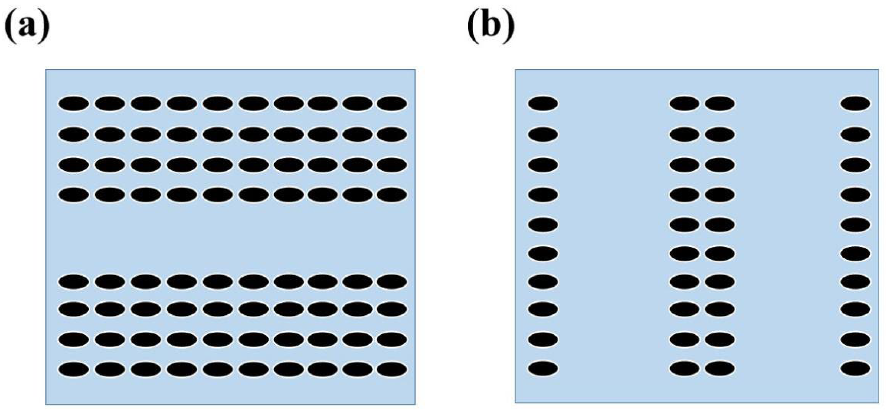
Figure 14.
The arrangement modes of two different types of photonic crystals with vacancy defects.

Figure 15.
The arrangements of two different types of photonic crystals with vacancy line defects.

Figure 16.
Comparison of absorption efficiency of air hole, GaAs column, InAs column and pure a-SiC absorption layer.
Figure 16.
Comparison of absorption efficiency of air hole, GaAs column, InAs column and pure a-SiC absorption layer.

Figure 17.
The changes of absorption efficiency of absorption layer with incident Angle.


Table 1.
The relationship between absorption efficiency of absorption layer of two different scatterer types and D.
Table 1.
The relationship between absorption efficiency of absorption layer of two different scatterer types and D.
| Parameter D | Absorptivity of Air Hole | Absorptivity of GaAs Column |
|---|---|---|
| 0.1 μm | 95.33% | 95.49% |
| 0.2 μm | 95.21% | 95.43% |
| 0.3 μm | 95.06% | 95.35% |
| 0.4 μm | 94.87% | 95.27% |
| 0.5 μm | 94.64% | 95.16% |
| 0.6 μm | 93.69% | 94.98% |
| 0.7 μm | 90.88% | 94.69% |
| 0.8 μm | 89.03% | 94.34% |
| 0.9 μm | 75.20% | 93.80% |
| 1.0 μm | 69.90% | 93.46% |
Table 2.
The relationship between absorption efficiency of absorption layer with two different scatterer types and T.
Table 2.
The relationship between absorption efficiency of absorption layer with two different scatterer types and T.
| Parameter T | Absorptivity of Air Hole | Absorptivity of GaAs Column |
|---|---|---|
| 0.2 μm | 76.84% | 93.79% |
| 0.4 μm | 94.77% | 95.22% |
| 0.6 μm | 95.06% | 95.35% |
| 0.8 μm | 95.17% | 95.41% |
| 1.0 μm | 95.23% | 95.44% |
| 1.2 μm | 95.27% | 95.46% |
| 1.4 μm | 95.29% | 95.47% |
| 1.6 μm | 95.31% | 95.48% |
| 1.8 μm | 95.33% | 95.49% |
| 2.0 μm | 95.34% | 95.49% |
Table 3.
The relationship between absorption efficiency of absorption layers with two different types of scatterers and H.
Table 3.
The relationship between absorption efficiency of absorption layers with two different types of scatterers and H.
| Parameter H | Absorptivity of Air Hole | Absorptivity of GaAs Column |
|---|---|---|
| 0.1 μm | 58.61% | 59.67% |
| 0.2 μm | 76.39% | 76.94% |
| 0.3 μm | 85.13% | 85.49% |
| 0.4 μm | 90.16% | 90.42% |
| 0.5 μm | 93.29% | 93.49% |
| 0.6 μm | 95.33% | 95.49% |
| 0.7 μm | 96.69% | 96.82% |
| 0.8 μm | 97.63% | 97.74% |
| 0.9 μm | 98.23% | 98.37% |
| 1.0 μm | 98.75% | 98.82% |
Table 4.
The relationship between absorption efficiency of absorption layers with two different types of scatterers and E.
Table 4.
The relationship between absorption efficiency of absorption layers with two different types of scatterers and E.
| Parameter E | Absorptivity of Air Hole | Absorptivity of GaAs Column |
|---|---|---|
| 0 | 95.3255% | 95.4876% |
| 0.1 | 95.3336% | 95.4902% |
| 0.2 | 95.3427% | 95.4936% |
| 0.3 | 95.3518% | 95.4970% |
| 0.4 | 95.3609% | 95.5006% |
| 0.5 | 95.3720% | 95.5058% |
| 0.6 | 95.3847% | 95.5126% |
| 0.7 | 95.3941% | 95.5179% |
| 0.8 | 95.4112% | 95.5285% |
| 0.9 | 95.4411% | 95.5474% |
| 1.0 | 95.4737% | 95.7005% |
Table 5.
The relationship between absorption efficiency of the absorption layer with elliptic ring scatterers and U.
Table 5.
The relationship between absorption efficiency of the absorption layer with elliptic ring scatterers and U.
| Parameter U | Parameter P (μm) | Parameter Q (μm) | Parameter M (μm) | Parameter N (μm) | Absorptivity |
|---|---|---|---|---|---|
| 2 | 0.1 | 0.05 | 0.2 | 0.10 | 95.70% |
| 3 | 0.1 | 0.05 | 0.3 | 0.15 | 95.68% |
| 4 | 0.1 | 0.05 | 0.4 | 0.20 | 95.67% |
| 5 | 0.1 | 0.05 | 0.5 | 0.25 | 94.78% |
| 6 | 0.1 | 0.05 | 0.6 | 0.30 | 93.50% |
Table 6.
The relationship between the absorption efficiency of the absorption layer with elliptic ring scatterers and V.
Table 6.
The relationship between the absorption efficiency of the absorption layer with elliptic ring scatterers and V.
| Parameter V | Parameter P (μm) | Parameter Q (μm) | Parameter M (μm) | Parameter N (μm) | Absorptivity |
|---|---|---|---|---|---|
| 1 | 0.1 | 0.05 | 0.6 | 0.30 | 93.50% |
| 2 | 0.2 | 0.10 | 0.6 | 0.30 | 94.03% |
| 3 | 0.3 | 0.15 | 0.6 | 0.30 | 94.76% |
| 4 | 0.4 | 0.20 | 0.6 | 0.30 | 95.44% |
| 5 | 0.5 | 0.25 | 0.6 | 0.30 | 95.49% |
Publisher’s Note: MDPI stays neutral with regard to jurisdictional claims in published maps and institutional affiliations. |
© 2022 by the authors. Licensee MDPI, Basel, Switzerland. This article is an open access article distributed under the terms and conditions of the Creative Commons Attribution (CC BY) license (https://creativecommons.org/licenses/by/4.0/).
Share and Cite
MDPI and ACS Style
Zhou, L.; Xu, Y.; Tan, S.; Liu, M.; Wan, Y. Simulation of Amorphous Silicon Carbide Photonic Crystal Absorption Layer for Solar Cells. Crystals 2022, 12, 665. https://doi.org/10.3390/cryst12050665
AMA Style
Zhou L, Xu Y, Tan S, Liu M, Wan Y. Simulation of Amorphous Silicon Carbide Photonic Crystal Absorption Layer for Solar Cells. Crystals. 2022; 12(5):665. https://doi.org/10.3390/cryst12050665
Chicago/Turabian StyleZhou, Lin, Yuwei Xu, Shuyu Tan, Meijie Liu, and Yong Wan. 2022. "Simulation of Amorphous Silicon Carbide Photonic Crystal Absorption Layer for Solar Cells" Crystals 12, no. 5: 665. https://doi.org/10.3390/cryst12050665
Note that from the first issue of 2016, this journal uses article numbers instead of page numbers. See further details here.