Review

Mini-LED Backlight Technology Progress for Liquid Crystal Display

1
State Key Laboratory of Luminescent Materials and Devices, Institute of Polymer Optoelectronic Materials and Devices, South China University of Technology, Guangzhou 510640, China
2
Huangpu Hydrogen Innovation Center, Guangzhou Key Laboratory for Clean Energy and Materials, School of Chemistry and Chemical Engineering, Guangzhou University, Guangzhou 510006, China
3
Guangzhou Color Screen Display Technology Co., Ltd., Guangzhou 510663, China
*
Authors to whom correspondence should be addressed.
Crystals 2022, 12(3), 313; https://doi.org/10.3390/cryst12030313
Submission received: 21 January 2022 / Revised: 9 February 2022 / Accepted: 15 February 2022 / Published: 23 February 2022
(This article belongs to the Special Issue Liquid Crystals in China)

Abstract

:
As consumers pursue higher display quality, Mini-LED backlight technology has become the focus of research in the current display field. With its size advantage (100–200 μm), it can achieve one-thousand-level divisional dimming, and it can also be combined with quantum dot technology to greatly improve the contrast, color gamut, dark state and other element of the display performance of LCD displays. Mini-LED backlight technology is undoubtedly the most ideal solution to realize a highly dynamic range display of LCD displays, and has been widely commercialized in many fields such as TVs, tablet computers, notebook computers, and car monitors. This review mainly introduces the efforts made by researchers to eliminate the halo effect, thinning of the backlight module and reducing the backlight power consumption. The application of quantum dot technology in backlight is also presented. We predict that the number of Mini-LED backlight partitions is expected to reach a level of more than 3000 in the future, further utilizing the advantages of the small size in local dimming, but it will also inevitably be challenged by some issues such as power consumption and heat dissipation.

1. Introduction

Display technology is one of the most important means for us to express and obtain information. It is ubiquitous in our daily life, including smartphones, tablet computers, TVs, projectors, and virtual/reality devices. As consumers continue to pursue higher display quality, a new word, high dynamic range (HDR) display, has appeared. Compared with ordinary images, high dynamic range images can provide greater dynamic range and image details, and better reproduce natural scenes. This often requires high peak brightness, excellent dark state, accurate grayscale, wide color gamut, and large bit depth [1,2]. There are currently two major technology camps, organic light-emitting diode (OLED) display technology and liquid crystal display (LCD) technology [3]. Whoever can provide a more ideal solution for HDR display will undoubtedly stand out among numerous display technology providers and become the leader of the next generation of display technologies. Although OLED displays have advantages in panel flexibility, black state, and response time [4], we believe that under the global trend of energy saving and emission reduction, LCDs with a longer life and lower cost are more promising display solutions in the future. Therefore, it is necessary to improve the performance of LCD displays.
Traditional LCD technology uses global dimming for backlight, which is to say, a single dimming segment covers the entire display. Therefore, each LC pixel cannot completely cut off the transmitted light from global dimming. As a result, it is difficult for traditional LCD to achieve a true dark state [5]. Besides, the traditional LCD contrast ratio (CR) is generally low. The possible reasons are the nonuniform alignment of the liquid crystal layer, the scattering of the color filters (CFs), and the diffraction from the pixelated electrodes [6]. These all limit the further improvement of the performance of the liquid crystal display. Researchers have been working hard to improve LCD display performance. An ideal solution that has been widely recognized and used is the local dimming backlight, using Mini-LED as the backlight source. Mini-LED is a kind of LED chip with a size between 100–200 microns [7]. Compared with the LED chips used in traditional backlight, it has a smaller size, thus providing a finer dimming. The local dimming backlight divides the backlight area into many independent dimming segments to realize each local dimming area’s independent brightness and extinction [8]. This method can better match the brightness required by each area to display the image, thereby achieving HDR display, and reducing power consumption and costs. However, there are still some problems that hinder the further improvement of local dimming LCD performance. The halo effect is a major problem that reduces the image quality of LCD, as shown in Figure 1. We can see the serious halo effect from the right part of Figure 1 in the red mark area. It can be divided into two types according to the causes. Due to the mismatch of the size between the backlight dimming area and pixel, there would be light leakage to the front panel, causing the halo effect called “Halo1”. The other is caused by the light leakage from the bright area of backlight unit (BLU) to the adjacent dark areas, called “Halo2” [9,10,11]. A schematic diagram of the two types of the halo effect is shown in Figure 2. The blue line is the light intensity curve of a local dimming area; the yellow line is the light intensity curve of the dimming area after being modulated by the LCD; the green line is the actual light intensity curve obtained by the corresponding pixel in the dimming area.
Direct-lit backlight is still the most commonly used backlighting method for LCD. It usually uses a sufficiently thick diffuser plate or leaves a large enough air gap between the backplane and the diffuser plate to convert the point light source into a uniform surface light source [13]. Both the diffuser and the air gap increase the thickness of the backlight module. The large increase in the number of Mini-LEDs can achieve uniform illumination and reduce the module thickness. However, that will lead to a higher cost, which hinders the development of LCD to ultra-thin displays. In addition, how to eliminate the “hot spots” generated in the process of reducing the module thickness is also a challenge [14,15].
A Mini-LED backlight unit can be driven by an active matrix (AM) or passive matrix (PM) based on the thin-film transistor (TFT) backplane [16]. When the PM driving method is used, the control ICs for PM driving can only drive a limited number of Mini-LEDs. So, a large number of control ICs are usually needed, leading to higher costs and the larger printed circuit board. (PCB) AM driving can eliminate the need for a large number of ICs. However, due to the low transmittance of LCD, the current of Mini-LED must be increased to several milli-Ampere (mA) to display the required brightness of the image [17]. In that case, power consumption in the power source lines will also increase. Thus, regardless of the driving method, power consumption is a concern that has to be considered. In addition, for a normal LCD, most of the backlight is absorbed by the polarizers, color filters, and other LCD components. As a result, less than 5~10% of the light is available for displaying images, which causes high amounts of energy waste [18]. Therefore, we believe that the optimization of driving circuits and the improvement of LCD components are two important research directions for researchers to reduce the power consumption of Mini-LED LCD backlight.
Focusing on three main concerns in Mini-LED backlight LCDs, namely the halo effect, backlight module thickness and power consumption, this paper reviews the research progress of Mini-LED backlight technology and analyzes and compares the advantages and limitations of different solutions. We also introduce the application of quantum dot technology in backlight from the perspective of structure. Finally, we introduce some cutting-edge commercial products equipped with Mini-LED backlight technology and make a brief prediction about the future of Mini-LED backlight.

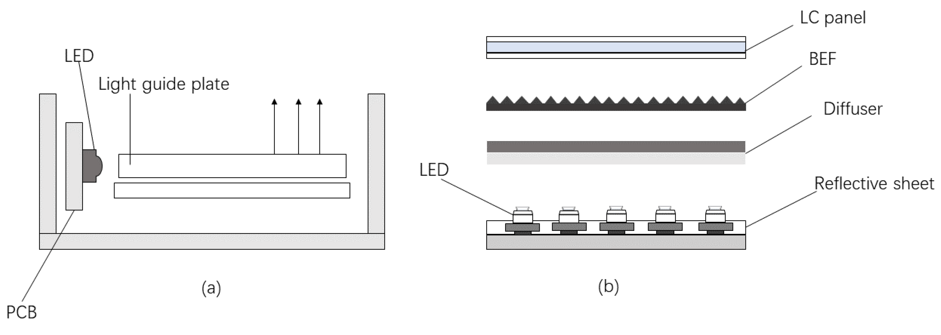
2. Mini-LED Backlight LCD System

There are two traditional backlight methods commonly used in LCD, including edge-lit backlight and direct-lit backlight, as shown in Figure 3a,b. The edge-lit Mini-LED backlight unit (BLU) installs the light sources on the side of the light guide plate (LGP). The incident light is exported through a scattering dots array on LGP and then spread to the LC layer to provide uniform light output [19,20]. The light sources of the direct-lit Mini-LED BLUs are regularly arranged on the backplane to form a Mini-LED array to regulate the brightness of the dimming unit [21]. Both two types of dimming units have their advantages and disadvantages. The edge-lit Mini-LED BLU has a relatively thin thickness and requires fewer light sources to achieve uniform light, so the power consumption caused by dimming is also relatively low. However, due to the position of the light source, the edge-lit BLU is mostly limited to one-dimensional dimming [22]. Although recent studies have achieved two-dimensional dimming of the edge-lit backlight [23], its application is far less extensive than the direct-lit type. The direct-lit Mini-LED BLU can take advantage of the small size of Mini-LED to divide the backlight area into more dimming blocks, providing higher dimming quality. Deng et al. have produced an LCD with a performance comparable to OLED displays [24]. It can achieve peak brightness above 1000 units and maximum local contrast over 3,000,000. However, since the direct-lit backlight relies on the diffuser to perform uniform light, the thickness of the system using direct-lit dimming is generally thick [21].
Despite the differences in the structure, the modulation process of the light after being emitted from BLU is identical. Using a picture of the candle as an example, Tan et al. briefly describes the modulation process of the light after being emitted from the BLU [25]. Taking direct-lit backlight as an example, Mini-LEDs in each dimming zone were first set to different gray levels according to the image content, as in Figure 4A. Then, the light was evenly diffused to the LC panel after passing through the diffuser, forming a preliminary simulated brightness distribution, as in Figure 4B. Finally, each pixel was modulated through the LC panel R/G/B channel to achieve a full-color image display, as in Figure 4C.

3. Research Progress of Mini-LED Backlight

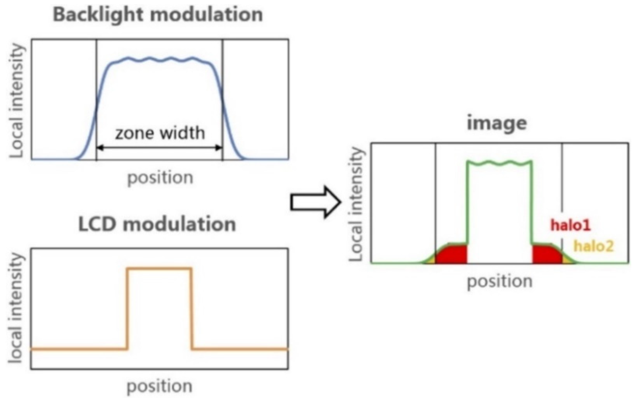
3.1. Solution to the Halo Effect

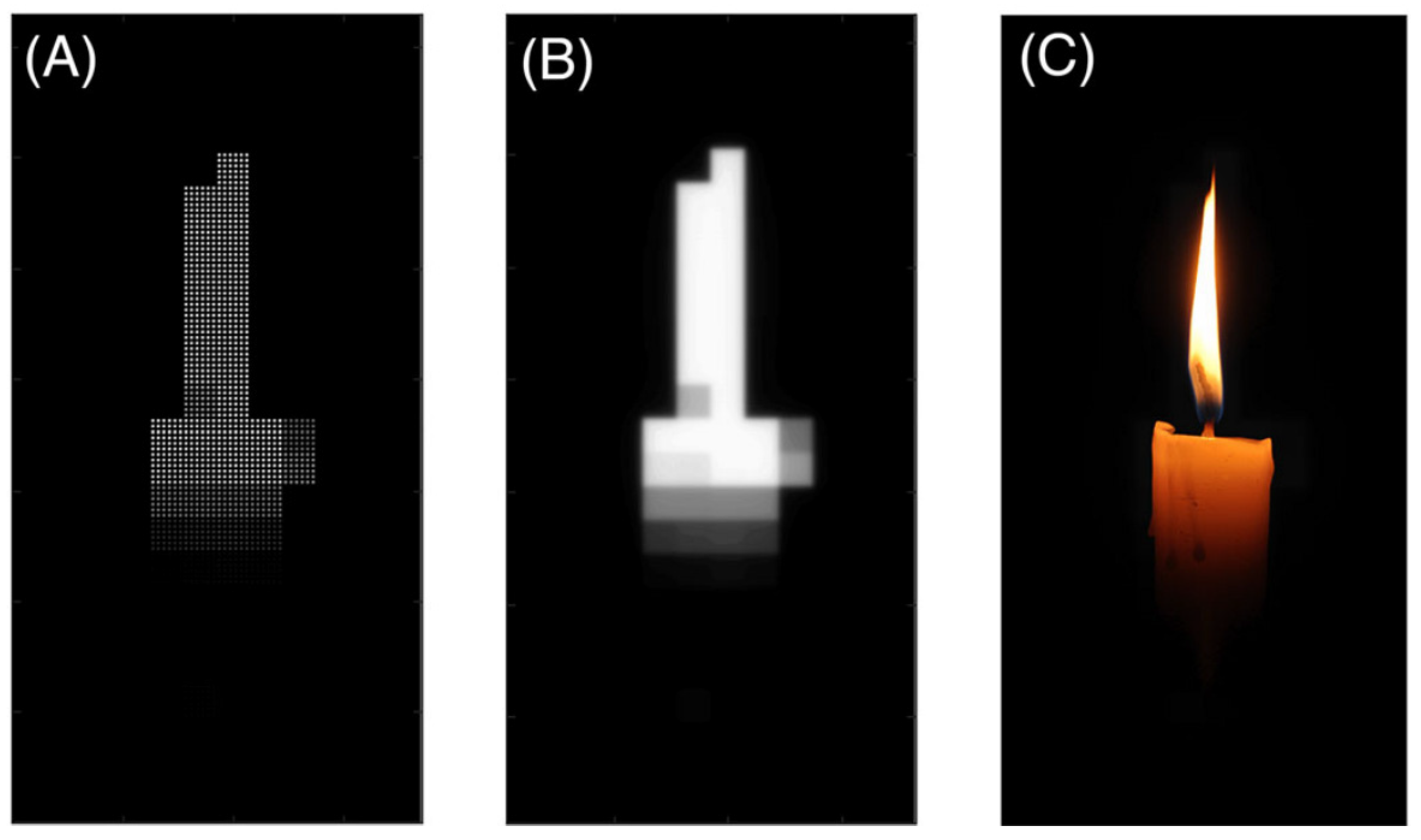
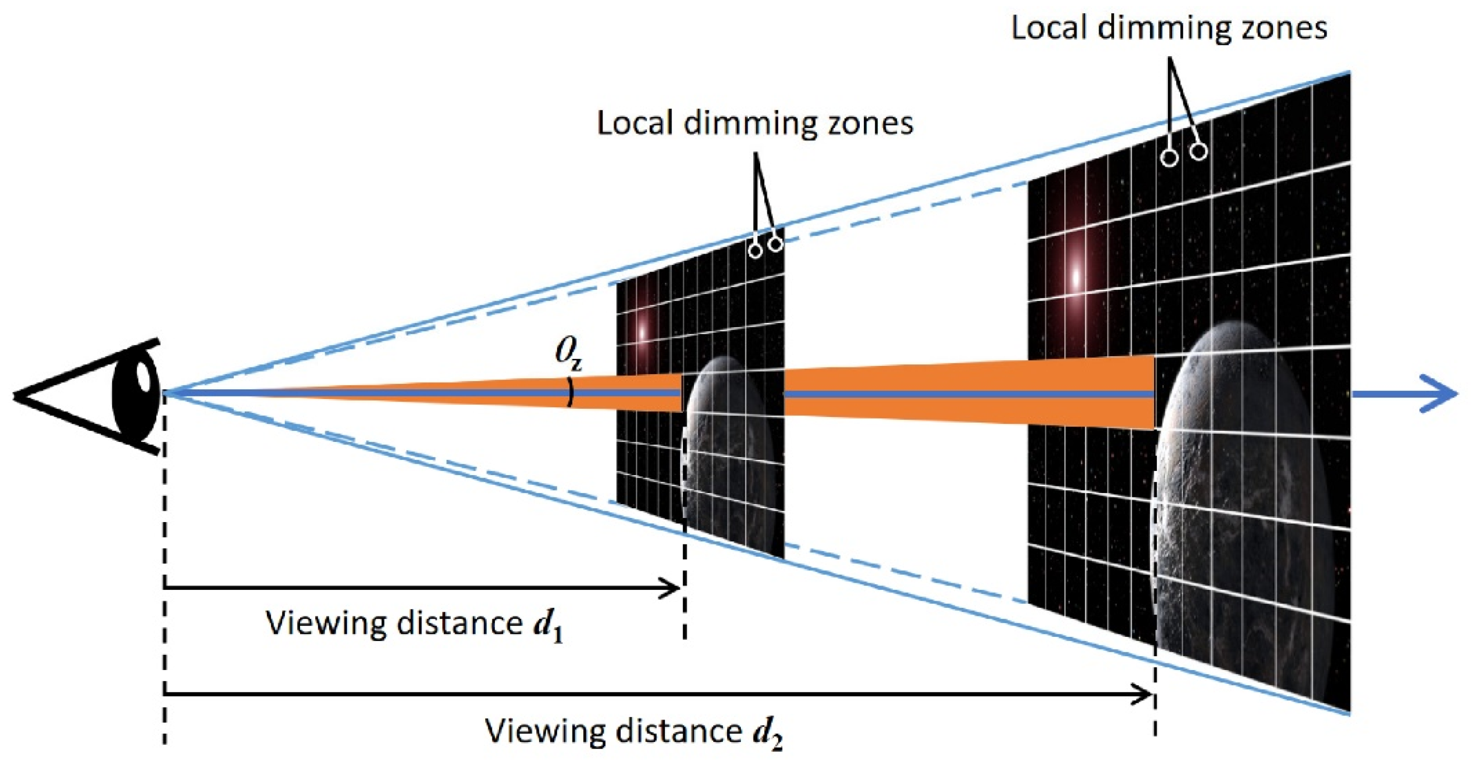
3.1.1. Presentation of the Assessment Methodology

To achieve a more intuitive perception of the halo effect, researchers developed a series of models to evaluate the halo effect in the local dimming system and proposed some important evaluation parameters [12,25,26,27,28]. An important commonly used evaluation parameter is the LabPSNR, proposed based on the peak signal-to-noise ratio (PSNR) in the CIE 1976 L*a*b* color space [8]. Tan et al. concluded from their experiments that less than 5% of observers can perceive the presence of the halo effect when the LabPSNR is greater than 47.4 dB [25]. That means the halo effect is suppressed to an imperceptible level. This finding formulated a reference standard for the suppression of the halo effect.
Based on this study, Hsiang et al. proposed a new D-value function and the LocalPSNR which is similar to the LabPSNR to better evaluate the halo effect [27]. In the D-value function, the D-value is defined as the ratio of the local contrast ratio and local average luminance. It can reflect the ease of observing the halo effect by the human vision system (HVS). A larger D-value of a region indicates that the halo effect in that region is more severe and more easily perceived by the HVS. When evaluating images, we can use the D-value function to find regions in which the halo effect is more easily detected by the HVS. Then, we can take advantage of the PSNR in these regions to quantitatively analyze the halo effect in them. The PSNR in these local areas is defined as LocalPSNR. This evaluation process allows for the exclusion of the influence of pixels far from the areas where the halo appears, making the evaluation system more accurate. These parameters can be used as a guide to find methods to suppress the halo effect.

3.1.2. Some Effective Solutions

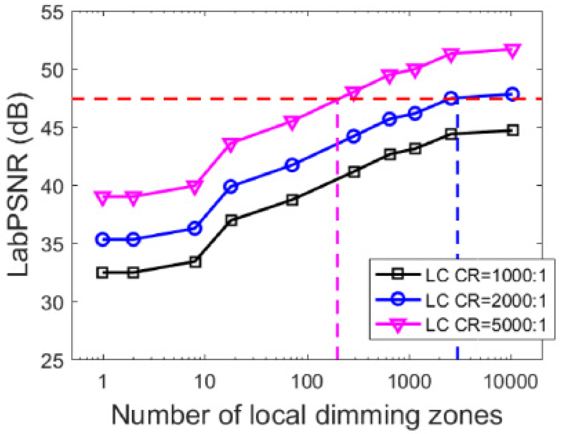
Increase the LC CR and Number of Local Dimming Zones

Hoffman et al. designed four experiments to simulate the dynamic contrast ratio of the model [29]. They evaluated the contribution of the number of the local dimming zones and the native panel contrast to the image quality. The results demonstrated that increasing the number of local dimming areas and the LC CR is beneficial to improve the image quality for HDR display. Based on this experiment, Tan et al. evaluated the image quality of the candle image shown in Figure 4 [25]. By varying the number of local dimming zones and the LC CR, they found that increasing the LC CR at the same number of local dimming zones or increasing the number of dimming zones at the same LC contrast both increased the LabPSNR value of the image. It shows that the image quality was improved and the halo effect was suppressed. The simulation results are shown in Figure 5. They used 47.4 dB as a criterion to estimate the number of dimming zones required (as shown by the red dotted line in Figure 5). For a LCD with CR ≈ 1000:1, even 10,000 local dimming zones still cannot achieve a good suppression effect. For a LCD with CR≈2000:1, the required local dimming zones is reduced to 3000 (as shown by the blue dotted line in Figure 5). When the LCD contrast is increased to 5000:1, an unnoticeable halo effect can be achieved at only about 200 local dimming zones (as shown by the pink dotted line in Figure 5). Besides, the number of LEDs in a single local dimming zone also affects the image quality. When using the same number of Mini-LEDs, a smaller number of LEDs in a single local dimming zone means a larger number of local dimming zones, which can lead to a higher LabPSNR.
Furthermore, they also revealed more detailed effects of the two measures. The number of local dimming zones mainly affects the area where the halo effect arises, while the LC CR mainly affects the local image distortion [25]. Although their experiments were based on a small-sized smartphone display with a viewing distance of 25 cm, the analysis and conclusions can also be applied to other display devices with different sizes and resolutions. All that needs to be done is to simply convert the results from the spatial domain to the angular domain, as shown in Figure 6.
However, the limitation of this approach is that it does not always work. For images with a good mixture of bright and dark pixels, this approach will provide very limited help in improving the image quality when the size of the local dimming zone is much larger than that of the uniform luminance block. This can be judged using the D-value function mentioned above. Local dimming will also fail to improve the image quality for images with two extreme cases of larger or smaller D-value [25,27].

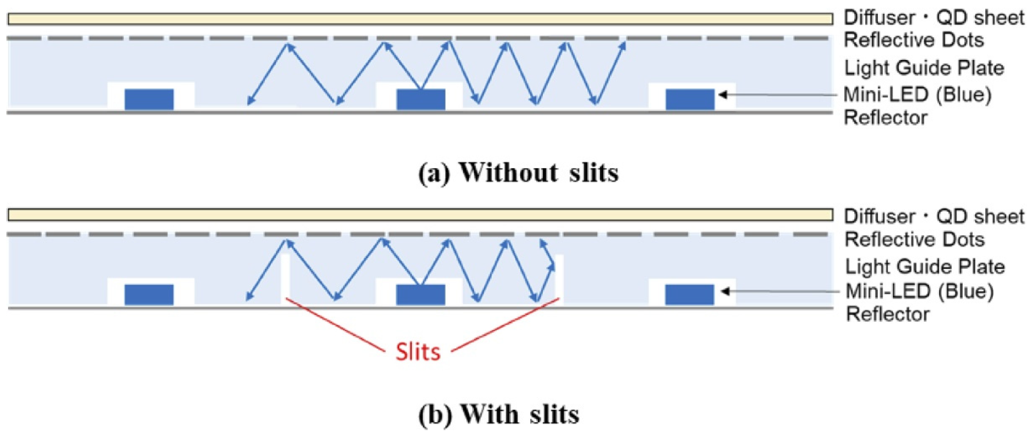
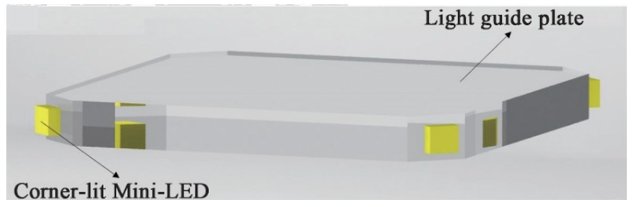
LED Light Expansion and Local Light Confinement

The LED is a Lambert-type light source. However, influenced by a variety of factors, the light distribution expands into a Gaussian-like type after light diffusion. Tan et al. used the Gaussian function to fit the expanded single-LED light profile [30]. They found that the smaller LED emitting aperture and shorter optical distance (OD) could obtain better image fidelity (high LabPSNR values). However, that would also raise issues such as impaired backlight uniformity and thermal management. Thus, choosing the suitable LED emitting aperture and OD can suppress the halo effect while ensuring a high degree of backlight uniformity.
The “Halo2” is caused by the interaction between adjacent dimming zones. Therefore, reducing the optical crosstalk in adjacent zones can essentially suppress the “Halo2”. Common measures for this process include adding optical structures such as bank isolation [31] or lens collimation [32]. A specific approach is to cut slits in the LGP at the boundary of each dimming segment as shown in Figure 7 [33]. The addition of slits can effectively reduce the crosstalk between adjacent local dimming areas and suppress the halo effect. The basic principle of these measures is to achieve local light confinement.
Except for the measures mentioned above, the improvement of the dimming algorithm is also an effective method used to suppress the halo effect [34,35,36,37]. Changes in objective factors such as the increase in ambient light can also mitigate the halo effect to some extent [38,39].

3.2. Thinning the Backlight Module

Reducing the thickness of backlight modules to improve the competitiveness of LCD in the field of ultra-thin dis play and the mobile display has been the pursuit of the LCD camp. In the second part, we have introduced two structures commonly used in traditional LCD backlight. However, none of them are ideal backlight solutions. The backlight we require is supposed to achieve both uniform backlight and the thin backlight module. For the direct-lit backlight system, uniform illumination can only be achieved at the expense of thickness. For the edge-lit backlight system, though the BLU can be made very thin, the quality of backlight is not so good. Therefore, researchers continue to upgrade the original backlight structure, or develop new backlight solutions, striving to develop the most ideal backlight solutions.

3.2.1. Some Important Parameters

Two important parameters of evaluating the thickness of a direct-lit backlight module are the distance between the light source and the receiving surface, called the optical distance (OD), and the LED array alignment pitch, called “Pitch” [40]. A smaller OD value means a thinner backlight module and a larger Pitch value means a smaller number of LEDs are used. Uniform illumination distribution is a prerequisite for all optimization strategies. Under this premise, we want to reduce the thickness of the backlight module as much as possible. The illuminance distribution function can be used to calculate and observe the variation of illuminance uniformity as the thickness changes [41]. Alternatively, we can use the MATLAB software (MathWorks Inc, Albuquerque, NM, USA) to build mathematical models to solve OD and visual luminance uniformity [42]. The industry usually uses the ratio of OD and Pitch, H:P, to describe the relationship between backlight module cost and thickness [43]. A smaller H:P value means a thinner backlight module and the use of fewer LED chips. Blindly using a large number of LEDs to reduce the thickness is undesirable and will lead to a dramatic increase in cost.

3.2.2. Research Progress of Module Thinning

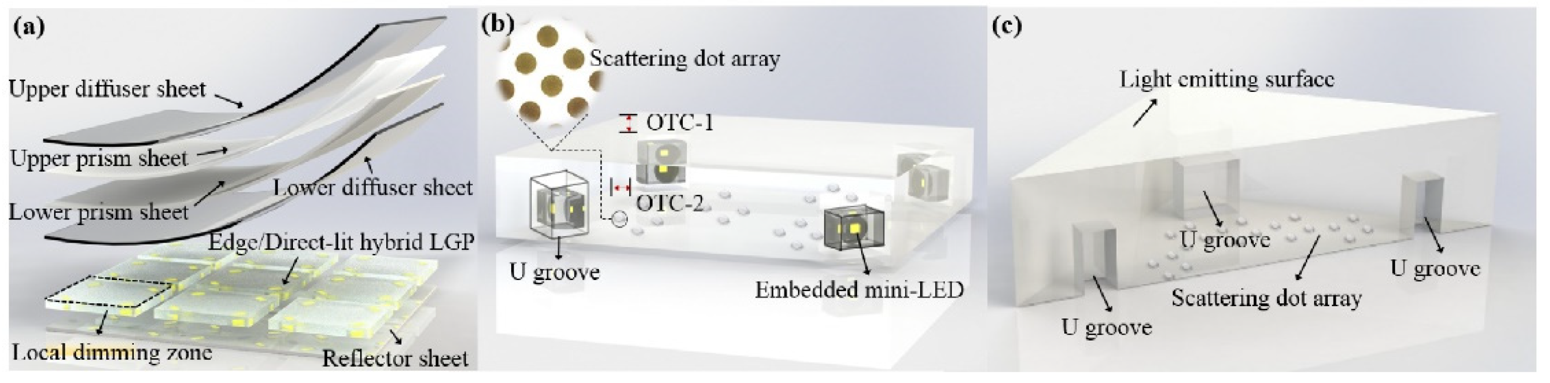
Innovative Backlight Methods

The common direct-lit LED backlight usually uses lenses to expand the LED illumination range to reduce the number of LEDs used [43]. However, due to the existence of a certain thickness of the lens, it failed to thin the backlight module. Based on this, we can try to expand the LED illumination range without using the lens. This probably allows for uniform illumination with a small number of LEDs while reducing thickness.
The proposal of some structures different from direct-lit and edge-lit backlight seems to be able to achieve this requirement [21,44]. In the new type of dimming unit called corner-lit type (Figure 8) BLU, the four corners of the regular LGP are smoothed and polished to form a flat light incident surface. The Mini-LED light sources are placed at the corner area of the LGP. The light is guided into the LGP and then uniform illuminance and high beam utilization can be achieved under the effect of the scattering dots at the bottom of the patterned LGP. Similar to the corner-lit BLU, Chen et al. proposed an edge/direct-lit hybrid backlight method [44]. The structure schematic is shown in Figure 9. The dimming principle is basically the same as the corner-lit dimming. The difference is that Guo et al. also designed optical transmission channels (OTC) at the four corners of the sub-LGP to eliminate possible hot spots generated by the Mini-LED. On the one hand, the new dimming method only requires a small number of light sources placed in the corner area. Thus, the entire dimming unit thickness is thinner and the backlight power consumption is lower. On the other hand, the rational design of the bottom scattering dots of the LGP can achieve uniform light emission. Through the optimization of optical films and other structures, it can obtain considerable light efficiency. The development of new backlight structures is expected to open up new ideas for the research of ultrathin dimming units with low power consumption and high light utilization.
The core of these new backlight solutions is the improvement of the LGP. We believe that the innovative design of the LGP is an important link in the future development of ultra-thin LCDs. The theoretical model proposed by Jiang et al. can accurately and effectively provide the optimal value of the width and thickness of the LGP, as well as the optimal light extraction and uniformity [45]. This work can undoubtedly provide indispensable theoretical guidance for larger and thinner LGPs in the future.

Innovative Design of Optical Structure

There are also some innovative designs for the optical structure of the common direct-lit backlight. The structure of the Mini-LED backlight using the LGP with reflective dots is shown in Figure 10 [33]. The LGP above the Mini-LEDs is equipped with reflective dots and a reflector which are separately placed on the top and bottom surfaces. This structure achieves a wide illumination area of a single Mini-LED and high luminance uniformity, possessing great potential for use in mobile LCDs.
Batwing-type emission has a wider emission angle than Lambertian emission, which is undoubtedly more desirable. There are many ways to obtain batwing-type radiation mode. Zheng et al. added a specially designed micro structure film between the brightness enhancement film (BEF) and diffuser plate [14]. Shen et al. used the lattice patterned micro lens array optical films above the Mini-LED dimming array [46]. Some researchers also placed the translucent layer [47,48], which has reflective and transmissive properties, or the birefringent light-shaping film [49] on the Mini-LED chip. All these measures can modify the Mini-LED angular light intensity distribution to achieve batwing-type emission, but adding optical films may reduce the luminance efficiency. More effective solutions are to target the improvement of the Mini-LED chip package. Huang et al. replace the conventional chip scale package (CSP) [50,51] and surface-mount devices (SMD) package [52] with a new method called freeform-designed chip scale package (FDCSP). FDCSP could achieve batwing-like emission mode and obtain high luminous efficiency at the same time. Alternatively, the secondary package design is used to add a top shielding structure to the LED chip to allow more light to be emitted from the side of the LED to widen the emission angle [43].
In the process of thinning the direct-lit backlight module, if the OD is too short to allow for sufficient light diffusion, regular hotspots would appear in the backlight, the appearance of which was basically the same as Mini-LED distribution [14]. Expanding the illumination range of a single Mini-LED can eliminate hotspots to a degree. Kim et al. installed the triangular patterned reflective sheet between Mini-LED BLUs [41]. By increasing the illuminance between LEDs, hotspots can be suppressed to a very low level. This method is expected to be widely applied.

3.3. Reduction of Backlight Power Consumption

The reduction of power consumption is an important research focus in the field of LCD today. Backlight consumption accounts for about 80% of total power consumption [53]. Therefore, the key to developing more energy-efficient LCDs is to reduce backlight power consumption. In Section 3.2.2, we introduce some studies that can expand the light-emitting angle of Mini-LEDs. This enables Mini-LED backlight LCDs to require fewer backlight sources, which also reduces backlight power consumption to some extent. In this section, we focus on the progress researchers have made in driving circuits, LCD components, and algorithm.

3.3.1. Mini-LED Backlight Evaluation Parameters

Local dimming technology can greatly reduce LCD power consumption compared to the normal global backlight. However, considering the Mini-LED energy loss [54] and chip driving [9,17], the overall power consumption of the Mini-LED local dimming system still has room for optimization. The power consumption of the dimming system is affected by various factors such as panel size, display image content and brightness, and backlight efficiency. Therefore, the simple power-consumption value size is not very meaningful for evaluating the local dimming system. A more meaningful assessment method is to evaluate the power-consumption-reduction efficiency of a local dimming system, as in Equation (1) [26]. The P   L D O N is the power consumption when the local dimming function is turned on while the P   L D O F F is that when the function is down. The P   B L A C K is the power consumption generated by the work of other driving systems when the backlight is turned off. P   P C R reflects the power-consumption-reduction efficiency of the local dimming system.
P   P C R = ( 1 P   L D O N + P   B L A C K P   L D O F F P   B L A C K ) · 100 %

3.3.2. Various Solutions for Reducing Backlight Consumption

Design Difficulties and Solutions of Driving Circuits

Compared with ordinary high-brightness LEDs, Mini-LEDs have a lower luminous efficiency. Because LEDs have an optimal driving current density range, but Mini-LEDs have a small size, driving is limited [55]. This also brings greater challenges to the circuit design of driving Mini-LEDs. Mini-LED BLUs are usually driven by an active matrix (AM) or passive matrix (PM). Compared to PM driving, AM driving saves on the number of source ICs and reduces the size and complexity of the PCB [17]. It can also increase the resolution of the backlight module [56], thus being a better driving option. With respect to the driving circuit, Mini-LEDs are often driven by conventional 2T1C [56,57,58], as shown in Figure 11. However, this traditional driving circuit cannot solve various problems encountered in driving Mini-LED BLU. First of all, the thin-film transistor (TFT) used for driving is affected by the processing, resulting in threshold-voltage (VTH) variations [59,60,61]. In addition, the voltage on the power line will be affected by the intrinsic parasitic resistance. This will lead to the power line current-resistance drop/rise (I-R rise/drop) phenomenon [62]. These two main problems mean Mini-LED are unable to obtain a uniform driving current, which eventually causes a severe image mura. To solve these problems, researchers have tried to increase the number of Mini-LEDs driven by a set of driving circuits from one to four [57], at the cost of increasing the number of chips used. A more reasonable solution is to add an additional metal layer and optimize the current-crowding path without increasing the number of LEDs [56]. There are also some active matrix organic light-emitting diode (AMOLED) pixel circuits that can solve these problems [63,64,65,66,67,68]. However, applying these circuits to Mini-LED BLU cannot substantially reduce the power consumption.
Kimura et al. proposed a driving method using pulse-width modulation (PWM) [69]. This effective method can keep the driving current at the optimal luminous-efficacy point, resulting in greater energy saving. However, the current required for Mini-LED backlight must be at the milliampere level, which is difficult to achieve. In 2019, Kim et al. proposed another PWM driving circuit without a current source [70]. Although their circuit is more easily realizable, there are more stringent requirements to achieve the precise control of gray levels. Recently, some more excellent driver circuit designs have appeared. Lin et al. proposed a new Mini-LED backlight circuit, which uses the PWM driving method to reduce the power consumption [71]. This method compensates for the VTH variations of TFTs and VSS I-R rises on the power lines, while the VDD I-R drop is not taken into consideration. To further reduce the power consumption, only a single TFT is located in the driving current path, so the voltage across VDD and VSS can be shrunk. Under this scheme, Mini-LED can be operated at the best luminance-efficacy point, minimizing the power consumption of the circuit. In 2021, Deng et al. presented another AM driving circuit for reducing the power consumption of Mini-LED backlight LCDs by reducing the total voltage. The circuit can also compensate for variations in the VTH of TFTs and the VSS power line, providing highly uniform drive current for Mini-LED backlight. These two schemes are ideal driving schemes [17].

Improvement of LCD Components

In theory, after the LCD backlight module emits light, the polarizer absorbs at least 50% of the incident light, and the rest is transmitted as linearly polarized light. The color filter further absorbs at least two-thirds of the polarized light. The result is that less than 10% of the light emitted by the backlight module can pass through the LCD panel. Therefore, finding alternatives to polarizers and color filters to reduce backlight waste can increase backlight usage and, in turn, produce more energy-efficient LCDs. Two important research topics concern the development of polarized backlights and the reduction the absorption of color filters.
There are many ways to generate polarized backlight, such as dielectric confinement of optical electric field [72], anisotropic effective transition dipole moments [73]. In addition, several groups have proposed high-performance films that can be used for polarized backlight. Srivastava et al. demonstrated a photoaligned nanorod enhancement films (NREF) for color and polarization conversion for LCD backlight, promising to increase the optical efficiency of conventional LCDs by about 60% [74]. Lin et al. successfully fabricated a highly ordered perovskite nanowire (NW) array film [75]. The fabricated device has excellent optical efficiency and polarization properties, providing a new idea for reducing the optical loss caused by polarizers.
Eliminating or reducing absorption in color filters is generally achieved in two ways, namely with a selectively reflecting filter or with a color-filter-free device. In the selectively reflecting color filter, the three subwavelength gratings correspond to the R, G, and B subpixels in the color filter [76]. Ideally, subwavelength gratings with a specific pitch transmit one primary color and completely reflect the other two. In fact, however, subwavelength gratings cannot fully reflect the other two primary colors, and often require additional absorbing color filters to assist. This not only makes the fabrication process of the sub-wavelength grating complicated, but the effect of improving the transmittance is not as good as that of the color-filter-free device.
Color-filter-free devices include the field sequential color display (FSCD) and color separation display. FSCDs synthesize full color images by rapidly displaying red, green and blue field images in chronological order [77]. In theory, without filters, FSCD can display three times the screen resolution and light transmission efficiency with a wider color gamut at a lower energy and material cost [78]. Yudai et al. developed a highly transparent color LCD using a FSC driving method, eliminating color filters and polarizers [79]. The product finally achieves excellent characteristics, such as high transmittance (80%), wide color gamut, and fast response time. The new Polymer-stabilized blue phase liquid crystal (PS-BPLC) developed by Huang et al. can further optimize the performance of FSCD [80]. The simulation results achieved single TFT addressing at a lower operating voltage of 15 V and a high transmission rate of 74%. Low voltage is beneficial for reducing overall power consumption, and single TFT addressing is good for improving optical efficiency, both of which are we need to reduce power consumption. However, there is still room for development in terms of color decomposition and scanning speed of FCSD.
The color separation display divides the light emitted by the backlight module into three primary colors (R G B) to pass through the corresponding sub-pixels, thereby significantly increasing the overall transmittance. According to the working principle, Teng et al. divide it into the following two types: diffractive optics and geometric optics [81]. In practical applications of color-separation displays using diffractive optics, a small-pitch grating is often added to facilitate the separation of the three primary colors. This reduces the light-transmission efficiency and the feasibility of the solution. Besides, due to the fact that grating is very sensitive to the wavelength of the incident light, this scheme is not suitable for broadband light sources. Although the geometrical optics method is less sensitive to wavelengths, it also has the fatal disadvantage that the primaries emerging out of the LC panel at their respective angles leads to color unevenness for the observer in the angular space.
The most ideal solution is the combination of polarized backlight and the color-filter-free device, which can greatly improve the optical efficiency of LCD and reduce power consumption. The device proposed by Teng et al. [81], which combines a polarized color-separating backlight and a color-filter-free LC panel, achieves a high optical efficiency (33.75%) that is approximately four times that of a conventional LCD. At the same time, the thickness of this module mainly depends on the light-emitting area of the LED, so the application of Mini-LED as a backlight source can further reduce the overall thickness. This solution is undoubtedly a very ideal Mini-LED backlight solution, which not only improves the optical efficiency, reduces power consumption, but also helps to reduce the overall backlight module.
In addition to the two aspects mentioned above, the improvement of the backlight source itself also plays an important role in reducing power consumption. The optimization of the packaging method of the Mini-LED chip [40,50,51] and the design of the LED sidewall structure [82,83] can also improve the Mini-LED light extraction efficiency, thus helping to create a more energy-efficient Mini-LED BLU.

Algorithm Optimization

Another important way to reduce BLU power consumption is to improve the dimming algorithm. The ideal algorithm should balance the efficiency and display quality. Researchers have proposed a new optimization algorithm by modeling and analyzing the backlight intensity and LC layer transmittance [8]. This algorithm can achieve lower power consumption with the same display quality or higher display-image quality with the same power consumption. There are also other algorithms with similar effects. Zhang et al. proposed an improved shuffled frog leaping algorithm [84] and an improved greedy algorithm [85], both of which can better balance image quality and power consumption. The disadvantage is that the former has a longer execution time, while the experimental analysis of the latter is based on simulation only, lacking verification based on the real dimming system. Cui et al. proposed a backlight spectral optimization algorithm based on linear programming, aiming at maximizing the luminous efficiency of the backlight [86]. By constructing a linear programming model, the theoretical maximum value of the spectral luminous efficiency of the backlight can be calculated. This was found through calculations that the theoretical light efficiency maximum can be more easily approached using narrow-bandwidth light sources such as lasers and quantum dot materials. These developments provide a design reference and characteristic standard for future low-power backlight LCDs.

4. Combination of the Mini-LED Backlight and Quantum Dot

There are various ways to obtain the white light needed for the LED backlight. The most common is to use blue LEDs with yellow phosphor. Blue light activates yellow phosphor to produce yellow light, and then the yellow light is mixed with the blue light, forming white light as a result. However, the color purity obtained by phosphor materials is usually low, and the final color gamut is not high enough. In contrast, nano-semiconductor quantum dot (QD) materials have narrow half-peak widths, tunable spectra, and longer life span. The use of QDs in the backlight can bring a wider color gamut, higher optical efficiency, enhanced ambient contrast, and smaller color shift, and can also effectively reduce costs [87,88,89,90]. With these advantages, quantum dots are rapidly gaining research attention in the LCD field.
According to the different positions of quantum dots in the LCD backlight structure, quantum-dot backlight technology is mainly divided into the following three types: QDs On-Chip structure in which quantum dots replace phosphor materials and are packaged directly with blue LED chips [91]; QDs On-Surface structure in which QDs are encapsulated in two layers of water and an oxygen barrier film to form a quantum dot film (called Quantum Dots Enhancement Film [92]) and then laminated to the top of the light guide [93]; QDs On-Edge structure in which QDs are encapsulated in a special glass tube and installed at the incidence of the backlight LED [94]. The schematic diagram of the three structures is shown in Figure 12.
The advantage of the QDs on-chip structure is that the amount of QD material is very small, which reduces the cost and simplifies the design of the optical structure [91]. However, this structure puts forward higher requirements on the stability of QDs. Considering the thermal energy produced by the LED chip and the light conversion process of the material itself, QD materials require high thermal stability [95,96]. The radiation power density of a 1 W blue LED chip can reach ~60 W/cm2, which also puts forward higher requirements for the photostability of QD materials. Ye et al. proposed that the future development of QD backlight technology with QDs On-chip structure can be made from two aspects [97]. One is to produce a blue LED chip with a lower working temperature, which is technically difficult; the other is to develop new materials with stable performance against high thermal radiation and light radiation. Specific measures include changing the structure of synthetic QDs (core–shell structure, alloying structure) and compounding QDs with inorganic materials, which are described in detail by Moon et al. [98] and Ji et al. [99].
The QDs on-surface structure greatly reduces the influence of the thermal radiation of the LED chip on the QD material [100]. The light radiation received by the QD material is also greatly reduced under the action of the LGP. The existing QD materials can fully meet the requirements. However, as the size of the backlight module increases, the amount of QD material also becomes larger, which directly leads to an increase in cost. To promote the wide application of backlight products with QDs on-surface structure, researchers should simplify the processing of QDEF films, and seek more suitable preparation materials to reduce costs.
QDs on-edge is a compromised version of the first two approaches. As early as 2013, the American company QD Vision worked with Sony to develop the first quantum dot TV [101]. The QD backlight structure used in it is the QDs On-Edge technology. This structure requires less quantum dots, but has stricter requirements for device assembly due to the fragile glass tube. At the same time, it also has the problem of low luminous efficiency, so it is gradually eliminated in practical applications.
In addition to the above three mainstream QD backlight structures, many researchers have also developed other new QD backlight structures. Gu et al. proposed an edge-lit backlight model with a innovative quantum dot slot in which QD microstructures are fabricated directly on the LGP [102]. Both Srivastava et al. [103] and Masaki Hasegawa et al. [104] applied CdSe quantum rods (QRs) in LCD backlight. There is also an innovative quantum dot bulk scattering diffuser scheme proposed by Ye et al.’s research group and a new edge-lit backlight technology for a high color gamut, low-cost Quantum dots network microstructure light guide plate [97].
For Mini-LEDs, due to the small chip size, only a small amount of phosphor can be coated, causing low color-conversion efficiency. This challenge can be effectively solved if Mini-LEDs are packaged by the method called “QDs On-Chip” [97]. Many teams have achieved the integration of red and green dual-emissive perovskite quantum dots films with blue Mini-LEDs [105,106,107]. Furthermore, researchers have already developed flexible backlight modules based on QDs [108]. We believe that the advantages brought by QDs will make up for the shortcomings of LCD technology when competing with OLED and other technologies.

5. Future Development of Mini-LED Backlight

In the previous introduction, we have shown the research progress of Mini-LED as LCD backlight in three aspects. In this part, we showcase some of the latest commercial products equipped with a Mini-LED backlight. We present the bright commercial prospects of Mini-LED backlight products and analyze the future development of Mini-LED backlight.
The Mini-LED is now almost always known to consumers in the form of backlight technology. Mini-LED backlight technology achieved commercial application for the first time in 2019, being used in Apple and Asus’ 32-inch professional displays and TCL’s TV products. After that, it immediately caused a shockwave in the display market. At the 9th China Information Technology Expo (CITE), TCL, Konka, and Skyworth all showcased their latest Min-LED TVs, while IVO and Tianma also introduced automotive displays using Mini-LED technology [109]. TCL’s “X12 8K Mini LED Starlight Smart Screen” has the best performance and occupies the top of the Mini-LED TV product pyramid. With the unique “OD zero” technology, it achieves ultra-thin screen thickness and can achieve up to 3000 nits of maximum brightness and 10,000,000:1 contrast ratio [109]. We also have reasons to believe that TCL will continue to lead the way in this industry. The myriad of Mini LED offerings indicates that that the development prospect is very bright for this technology. TrendForce’s latest investigations indicate that, in light of Apple’s foray into the high-end notebook computer market with the latest generation of MacBook Pro, the annual shipment of notebook computers equipped with Mini LED backlight for 2022 will likely reach five million units, a 213% YoY increase [110]. Both of the new MacBook Pro models are equipped with a Mini LED backlight, with about 8000–11,000 Mini LED chips divided across 2000–2600 local dimming zones, resulting in a 1,000,000:1 contrast ratio [110]. It is believed that in the near future, the number of Mini-LED backlight partitions is expected to increase to 3000 or even higher.
However, we also believe that a smaller chip size is not necessarily the most advantageous. When the chip size is too small and the dimming areas are too much, the design of the driver circuit, the huge amount of chip transfer, the backlight module power consumption, and heat dissipation are all serious challenges. We predict that there will be an optimal size of Mini-LED where the maximum number of dimming zones can be achieved to gain optimal backlight without presenting various other challenges. The optimal size of Mini-LED requires further exploration from researchers.

6. Conclusions

In this article, we reviewed the research progress of Mini-LED backlight technology. The efforts made by researchers to eliminate the halo effect, develop ultra-thin LCDs, and develop more energy-efficient LCDs are introduced. At the same time, various structures of quantum dot backlight are demonstrated. Finally, we show a series of commercial products equipped with Mini-LED backlight technology, and make a brief forecast of the future developments of this technology. The advantage of Mini-LED backlight technology is that Mini-LED can be regarded as a scaled-down version of traditional LED chips. Therefore, the manufacturing and application technology system has been perfected. However, the biggest bottleneck of this technology is still how to balance cost and backlight effect. In the long run, in order to improve the competitiveness of the LCD camp in the market competition with OLED, flexible display will be the next development direction of Mini-LED backlight.

Author Contributions

Conceptualization, Z.G. and W.X.; methodology, H.N. and R.Y.; software, W.Z. and J.X.; validation, C.G. and H.X.; formal analysis, R.Y.; investigation, C.G.; resources, D.L.; data curation, J.X.; writing—original draft preparation, Z.G. and H.X.; writing—review and editing, Z.G. and H.N.; visualization, W.X.; supervision, D.L.; project administration, W.X. and H.N.; funding acquisition, H.N. All authors have read and agreed to the published version of the manuscript.

Funding

This work was supported by National Natural Science Foundation of China (Grant No. 62074060), Guangdong Basic and Applied Basic Research Foundation (Grant No.2020B1515020032), Ji Hua Laboratory scientific research project (X190221TF191), 2021 Guangdong University Student Science and Technology Innovation Special Fund (“Climbing Plan” Special Fund) (No.pdjh2021b0036), College Students Innovation and Entrepreneurship Training Program (No.S202110561184) and Fundamental Research Funds for the Central Universities (No.2020ZYGXZR060).

Conflicts of Interest

The authors declare no conflict of interest.

References

  1. Kwon, J.-U.; Bang, S.; Kang, D.; Yoo, J.J. 65-2: The Required Attribute of Displays for High Dynamic Range. SID Symp. Dig. Tech. Pap. 2016, 47, 884–887. [Google Scholar] [CrossRef]
  2. Zhu, R.; Sarkar, A.; Emerton, N.; Large, T. 81-3: Reproducing High Dynamic Range Contents Adaptively based on Display Specifications. SID Symp. Dig. Tech. Pap. 2017, 48, 1188–1191. [Google Scholar] [CrossRef]
  3. Yu, C. Progress in display technologies and their applications. Chin. Opt. 2010, 3, 27. [Google Scholar]
  4. Chen, H.-W.; Lee, J.-H.; Lin, B.-Y.; Chen, S.; Wu, S.-T. Liquid crystal display and organic light-emitting diode display: Present status and future perspectives. Light. Sci. Appl. 2018, 7, 17168. [Google Scholar] [CrossRef] [PubMed]
  5. Hoffman, D.M.; Choi, M.; Xiong, W. 81-2: Visual Quality of Global Dimming Backlight with High Contrast Liquid Crystal Panel for High Dynamic Range Displays. SID Symp. Dig. Tech. Pap. 2017, 48, 1184–1187. [Google Scholar] [CrossRef]
  6. Chen, H.; Tan, G.; Li, M.-C.; Lee, S.-L.; Wu, S.-T. Depolarization effect in liquid crystal displays. Opt. Express 2017, 25, 11315–11328. [Google Scholar] [CrossRef] [Green Version]
  7. Wu, T.; Sher, C.-W.; Lin, Y.; Lee, C.-F.; Liang, S.; Lu, Y.; Chen, S.-W.H.; Guo, W.; Kuo, H.-C.; Chen, Z. Mini-LED and Micro-LED: Promising Candidates for the Next Generation Display Technology. Appl. Sci. 2018, 8, 1557. [Google Scholar] [CrossRef] [Green Version]
  8. Burini, N.; Nadernejad, E.; Korhonen, J.; Forchhammer, S.; Wu, X. Modeling Power-Constrained Optimal Backlight Dimming for Color Displays. J. Disp. Technol. 2013, 9, 656–665. [Google Scholar] [CrossRef] [Green Version]
  9. Xiao, J.; Fei, J.; Zheng, F.; Liu, Q.; Huo, W.; Li, J.; Mei, W.; Xu, H.; Zhang, S. Mini-LED backlight units on glass for 75-inch 8K resolution liquid crystal display. J. Soc. Inf. Disp. 2021, 1–7. [Google Scholar] [CrossRef]
  10. Li, J.; Liu, H.; Liu, L.; Li, D.; Yu, H.; Jia, L.; Hao, Y.; Sun, H. P-111: Halo guides the design of backlight partition in Mini-LED Display. In Proceedings of the SID Symposium Digest of Technical Papers; Wiley-Blackwell: Hoboken, NJ, USA, 2021; pp. 1158–1161. [Google Scholar]
  11. Ichioka, H.; Otoi, K.; Fujiwara, K.; Hashimoto, K.; Murakami, H.; Yamamoto, T. 50.3: Proposai of Evaluation Method for Local-Dimming Backlights. In Proceedings of the SID Symposium Digest of Technical Papers; Wiley-Blackwell: Hoboken, NJ, USA, 2010; pp. 750–753. [Google Scholar]
  12. Chen, C.-C.; Qiu, Y.-Y.; Zheng, W.-W.; Yu, G.; Chiu, C.-Y.; Zhao, B.; Zhang, X. 17-4: Evaluate and Upgrade Picture Quality of Local Dimming Mini-LED LCD. In Proceedings of the SID Symposium Digest of Technical Papers; Wiley-Blackwell: Hoboken, NJ, USA, 2020; pp. 235–238. [Google Scholar]
  13. Mi, X.-D.; Wu, J.-C.; Sun, H.-W.; Chen, M.; Varanytsia, A.; Han, S.; Allen, K.R.; Maurey, P.A.; Baker, D.L.; Tokar, J. 46-1: Patterned Glass Diffuser (PGD) for MiniLED Backlights. In Proceedings of the SID Symposium Digest of Technical Papers; Wiley-Blackwell: Hoboken, NJ, USA, 2021; pp. 620–623. [Google Scholar]
  14. Zheng, B.; Deng, Z.; Zheng, J.; Wu, L.; Yang, W.; Lin, Z.; Wang, H.; Shen, P.; Li, J. 41-2: Invited Paper: An Advanced High-Dynamic-Range LCD for Smartphones. In Proceedings of the SID Symposium Digest of Technical Papers; Wiley-Blackwell: Hoboken, NJ, USA, 2019; pp. 566–568. [Google Scholar]
  15. Rao, R.; Mos, B.; Overes, T.; Langendijk, E.H. Masking LED hot spots in a thin direct lit backlight unit using semitransparent and perforated masks. Opt. Commun. 2014, 315, 258–264. [Google Scholar] [CrossRef]
  16. Su, J.-J.; Huang, H.-Y.; Kuo, H.-P.; Lee, M.-H.; Chen, C.-W.; Liao, C.-H.; Chang, K.-C.; Wu, Y.-E.; Liau, W.-L. 17-1: Invited Paper: An Overview of Solutions for Achieving HDR LCDs. SID Symp. Dig. Tech. Pap. 2020, 51, 224–227. [Google Scholar] [CrossRef]
  17. Deng, M.-Y.; Hsiang, E.-L.; Yang, Q.; Tsai, C.-L.; Chen, B.-S.; Wu, C.-E.; Lee, M.-H.; Wu, S.-T.; Lin, C.-L. Reducing Power Consumption of Active-Matrix Mini-LED Backlit LCDs by Driving Circuit. IEEE Trans. Electron Devices 2021, 68, 2347–2354. [Google Scholar] [CrossRef]
  18. Feng, Z.; Wu, Y.; Surigalatu, B.; Zhang, X.; Chang, K.-C.; Borjigin, S. Large transparent display based on liquid crystal technology. Appl. Opt. 2020, 59, 4915–4920. [Google Scholar] [CrossRef] [PubMed]
  19. Jiang, Z.; Lv, C.; You, Y.; Liu, Z.; Xu, S.; Chen, E.; Ye, Y. Interactive design of scattering dots array on light guide plate for LCD backlight. In Proceedings of the 9th International Symposium on Advanced Optical Manufacturing and Testing Technologies: Advanced Optical Manufacturing Technologies, Chengdu, China, 16 January 2019; p. 108380X. [Google Scholar]
  20. Guo, Q.; Ye, Y.; Chen, E.; Xu, S. Two-step optimization for a pattern array to improve light extraction efficiency and uniformity in light guide plates. Appl. Opt. 2019, 58, 9178–9185. [Google Scholar] [CrossRef] [PubMed]
  21. Ju, G.; Qiong-xin, S.; Zong-zhao, J.; En-guo, C.; Tai-liang, G. Optical performance of local dimming backlight unit based on Mini-LED sources. Chin. J. Liq. Cryst. Disp. 2021, 36, 939–946. [Google Scholar]
  22. Yagi, S.; Miyata, H.; Kondo, N.; Ishida, T. 14-3: High Efficiency and Thin Backlight System Using an Advanced Light-guide with a Multi-prism Array. SID Symp. Dig. Tech. Pap. 2018, 49, 153–156. [Google Scholar] [CrossRef]
  23. Yoon, G.-W.; Bae, S.-W.; Lee, Y.-B.; Yoon, J.-B. Edge-lit LCD backlight unit for 2D local dimming. Opt. Express 2018, 26, 20802–20812. [Google Scholar] [CrossRef]
  24. Deng, Z.; Zheng, B.; Zheng, J.; Wu, L.; Yang, W.; Lin, Z.; Shen, P.; Li, J. 74-5: Late-News Paper: High Dynamic Range Incell LCD with Excellent Performance. SID Symp. Dig. Tech. Pap. 2018, 49, 996–998. [Google Scholar] [CrossRef]
  25. Tan, G.; Huang, Y.; Li, M.-C.; Lee, S.-L.; Wu, S.-T. High dynamic range liquid crystal displays with a mini-LED backlight. Opt. Express 2018, 26, 16572–16584. [Google Scholar] [CrossRef] [Green Version]
  26. Chen, H.; Ha, T.H.; Sung, J.H.; Kim, H.R.; Han, B.H. Evaluation of LCD local-dimming-backlight system. J. Soc. Inf. Disp. 2010, 18, 57–65. [Google Scholar] [CrossRef]
  27. Hsiang, E.-L.; Yang, Q.; He, Z.; Zou, J.; Wu, S.-T. Halo effect in high-dynamic-range mini-LED backlit LCDs. Opt. Express 2020, 28, 36822–36837. [Google Scholar] [CrossRef] [PubMed]
  28. Xia, Z.; Hu, F.; Cheng, C. Perceptual Artifacts on the Liquid Crystal Displays with a Mini-LED Backlight; Suzhou University of Science and Technology: Suzhou, China, 2019. [Google Scholar]
  29. Hoffman, D.M.; Stepien, N.N.; Xiong, W. The importance of native panel contrast and local dimming density on perceived image quality of high dynamic range displays. J. Soc. Inf. Disp. 2016, 24, 216–228. [Google Scholar] [CrossRef]
  30. Huang, Y.; Tan, G.; Gou, F.; Li, M.-C.; Lee, S.-L.; Wu, S.-T. Prospects and challenges of mini-LED and micro-LED displays. J. Soc. Inf. Disp. 2019, 27, 387–401. [Google Scholar] [CrossRef]
  31. Sun, C.-C.; Chien, W.-T.; Moreno, I.; Hsieh, C.-T.; Lin, M.-C.; Hsiao, S.-L.; Lee, X.-H. Calculating model of light transmission efficiency of diffusers attached to a lighting cavity. Opt. Express 2010, 18, 6137–6148. [Google Scholar] [CrossRef]
  32. Woodgate, G.J.; Harrold, J. P-101: Micro-Optical Systems for Micro-LED Displays. In Proceedings of the SID Symposium Digest of Technical Papers; Wiley-Blackwell: Hoboken, NJ, USA, 2018; pp. 1559–1562. [Google Scholar]
  33. Kikuchi, S.; Shibata, Y.; Ishinabe, T.; Fujikake, H. Thin mini-LED backlight using reflective mirror dots with high luminance uniformity for mobile LCDs. Opt. Express 2021, 29, 26724. [Google Scholar] [CrossRef]
  34. Chen, H.; Sung, J.; Ha, T.; Park, Y.; Hong, C. Backlight local dimming algorithm for high contrast LCD-TV. In Proceedings of the ASID, New Delhi, India, 8–12 October 2006; pp. 168–171. [Google Scholar]
  35. Hong, J.-J.; Kim, S.-E.; Song, W.-J. A clipping reduction algorithm using backlight luminance compensation for local dimming liquid crystal displays. IEEE Trans. Consum. Electron. 2010, 56, 240–246. [Google Scholar] [CrossRef]
  36. Shu, X.; Wu, X.; Forchhammer, S. Optimal local dimming for LC image formation with controllable backlighting. IEEE Trans. Image Process. 2012, 22, 166–173. [Google Scholar] [CrossRef]
  37. Kim, S.-E.; An, J.-Y.; Hong, J.-J.; Lee, T.W.; Kim, C.G.; Song, W.-J. How to reduce light leakage and clipping in local-dimming liquid-crystal displays. J. Soc. Inf. Disp. 2009, 17, 1051–1057. [Google Scholar] [CrossRef] [Green Version]
  38. Hsiang, E.-L.; Yang, Q.; He, Z.; Zou, J.; Wu, S.-T. 47-4: Student Paper: Ambient Light and Human Vision Effects on High-Dynamic-Range Displays. In Proceedings of the SID Symposium Digest of Technical Papers; Wiley-Blackwell: Hoboken, NJ, USA, 2021; pp. 646–649. [Google Scholar]
  39. Hsiang, E.-L.; Huang, Y.; Yang, Q.; Wu, S.-T. High Dynamic Range Mini-LED and Dual-Cell LCDs; University of Central Florida: Orlando, FL, USA, 2020. [Google Scholar]
  40. Huang, C.-H.; Kang, C.-Y.; Chang, S.-H.; Lin, C.-H.; Lin, C.-Y.; Wu, T.; Sher, C.-W.; Lin, C.-C.; Lee, P.-T.; Kuo, H.-C. Ultra-High Light Extraction Efficiency and Ultra-Thin Mini-LED Solution by Freeform Surface Chip Scale Package Array. Crystals 2019, 9, 202. [Google Scholar] [CrossRef] [Green Version]
  41. Kim, B.; Kim, J.; Ohm, W.-S.; Kang, S. Eliminating hotspots in a multi-chip LED array direct backlight system with optimal patterned reflectors for uniform illuminance and minimal system thickness. Opt. Express 2010, 18, 8595–8604. [Google Scholar] [CrossRef]
  42. Chang, K.; Yu, L.; Sang, J. P-5.13: Visual Luminance Uniformity and OD value calculation for Direct Type Mini-LED Backlight. SID Symp. Dig. Tech. Pap. 2019, 50, 750–752. [Google Scholar] [CrossRef]
  43. Li, F.; Zong, Z.; Zhang, N.; Mu, L.; Liu, X. 12.3: Research on Reducing H: P Value of Lensless Direct-lit Backlight Module. SID Symp. Dig. Tech. Pap. 2021, 52, 180–182. [Google Scholar] [CrossRef]
  44. Chen, E.; Guo, J.; Jiang, Z.; Shen, Q.; Ye, Y.; Xu, S.; Sun, J.; Yan, Q.; Guo, T. Edge/direct-lit hybrid mini-LED backlight with U-grooved light guiding plates for local dimming. Opt. Express 2021, 29, 12179–12194. [Google Scholar] [CrossRef] [PubMed]
  45. Jiang, Z.; Ye, Y.; Guo, J.; Pan, J.; Cao, X.; Guo, T.; Chen, E. Optimal dimension of edge-lit light guide plate based on light conduction analysis. Opt. Express 2021, 29, 18705–18719. [Google Scholar] [CrossRef] [PubMed]
  46. Shen, B.; Aspell, J.; Rinehart, T.; Patel, K.; Pope, M.; Walker, K. P-206: Late-News-Poster: Lattice Patterned Micro Lens Array (MLA) Optical Films for Mini-LED Back Light Units (BLUs). In Proceedings of the SID Symposium Digest of Technical Papers; Wiley-Blackwell: Hoboken, NJ, USA, 2020; pp. 1649–1651. [Google Scholar]
  47. Xu, L.; Ming, C.C.; Li, Y.; Fan, K.; Zhang, M.; Sun, H.; Guo, Z. Uniform Illumination Realized by Large Viewing Angle of Gallium Nitride-Based Mini-LED Chip With Translucent Sublayer Pairs. IEEE Access 2021, 9, 74713–74718. [Google Scholar] [CrossRef]
  48. Zhang, B.; Geng, X.; Han, B.; Qin, J.; Gao, L.; Sang, J. P-97: Research on the effect of simplified structure of mini-LED backlight module on luminous efficiency. SID Symp. Dig. Tech. Pap. 2019, 50, 1599–1601. [Google Scholar] [CrossRef]
  49. He, Z.; Yin, K.; Hsiang, E.L.; Li, M.C.; Lee, S.L.; Tien, K.C.; Wu, S.T. Birefringent light-shaping films for mini-LED backlights. J. Soc. Inf. Disp. 2020, 28, 476–482. [Google Scholar] [CrossRef]
  50. Lee, K.H.; Kim, S.H.; Lim, W.-S.; Song, J.-O.; Ryou, J.-H. Visible Light-Emitting Diodes with Thin-Film-Flip-Chip-Based Wafer-Level Chip-Scale Package Technology Using Anisotropic Conductive Film Bonding. IEEE Electron Device Lett. 2015, 36, 702–704. [Google Scholar] [CrossRef]
  51. Huang, C.-H.; Chen, K.-J.; Tsai, M.-T.; Shih, M.-H.; Sun, C.-W.; Lee, W.-I.; Lin, C.-C.; Kuo, H.C. High-efficiency and low assembly-dependent chip-scale package for white light-emitting diodes. J. Photon Energy 2015, 5, 057606. [Google Scholar] [CrossRef]
  52. Raypah, M.E.; Sodipo, B.K.; Devarajan, M.; Sulaiman, F. Estimation of Optical Power and Heat-Dissipation Factor of Low-Power SMD LED as a Function of Injection Current and Ambient Temperature. IEEE Trans. Electron Devices 2015, 63, 408–413. [Google Scholar] [CrossRef]
  53. Albrecht, M.; Karrenbauer, A.; Jung, T.; Xu, C. Sorted Sector Covering Combined with Image Condensation-An Efficient Method for Local Dimming of Direct-Lit and Edge-Lit LCDs. IEICE Trans. Electron. 2010, 93, 1556–1563. [Google Scholar] [CrossRef]
  54. Huang, C.-H.; Chang, S.H.; Liaw, B.-Y.; Liu, C.-Y.; Chou, C.-Y.; Zhou, J.-R.; Lin, C.-C.; Kuo, H.-C.; Song, L.-J.; Li, F. Research on a novel GaN-based converted mini-LED backlight module via a spectrum-decouple system. IEEE Access 2020, 8, 138823–138833. [Google Scholar] [CrossRef]
  55. Yang, X. Mini-LED Next Generation of Display. Optoelectron. Technol. 2018, 38, 149–150. [Google Scholar]
  56. Wu, Y.-E.; Lee, M.-H.; Lin, Y.-C.; Kuo, C.; Lin, Y.-H.; Huang, W.-M. 41-1: Invited Paper: Active Matrix Mini-LED Backlights for 1000PPI VR LCD. In Proceedings of the SID Symposium Digest of Technical Papers; Wiley-Blackwell: Hoboken, NJ, USA, 2019; pp. 562–565. [Google Scholar]
  57. Liu, B.; Liu, Q.; Li, J.; Zhu, F.; Xiao, J.; Zhang, X.; Zhou, H. An Active Matrix Mini-LEDs Backlight based on a-Si. In Proceedings of the SID Symposium Digest of Technical Papers; Wiley-Blackwell: Hoboken, NJ, USA, 2020; pp. 62–64. [Google Scholar]
  58. Xu, H.; Xiao, J.; Fei, J.; Zhao, R.; Wang, X.; Hao, S.; Qiu, Y.; Liu, J.; Li, Y.; Zhuang, J. 10-3: Invited Paper: AM MLED backlight units on glass for 75-inch LCD displays. In Proceedings of the SID Symposium Digest of Technical Papers; Wiley-Blackwell: Hoboken, NJ, USA, 2020; pp. 122–125. [Google Scholar]
  59. Guo, X.; Silva, S. Investigation on the Current Nonuniformity in Current-Mode TFT Active-Matrix Display Pixel Circuitry. IEEE Trans. Electron Devices 2005, 52, 2379–2385. [Google Scholar] [CrossRef]
  60. Nathan, A.; Chaji, G.; Ashtiani, S.J. Driving Schemes for a-Si and LTPS AMOLED Displays. J. Disp. Technol. 2005, 1, 267–277. [Google Scholar] [CrossRef]
  61. Keum, N.-H.; Chai, C.-C.; Hong, S.-K.; Kwon, O.-K. A Compensation Method for Variations in Subthreshold Slope and Threshold Voltage of Thin-Film Transistors for AMOLED Displays. IEEE J. Electron Devices Soc. 2019, 7, 462–469. [Google Scholar] [CrossRef]
  62. Lin, Y.-C.; Shieh, H.-P. Improvement of Brightness Uniformity by AC Driving Scheme for AMOLED Display. IEEE Electron Device Lett. 2004, 25, 728–730. [Google Scholar] [CrossRef]
  63. Lin, C.-L.; Hung, C.-C.; Chen, P.-S.; Lai, P.-C.; Cheng, M.-H. New Voltage-Programmed AMOLED Pixel Circuit to Compensate for Nonuniform Electrical Characteristics of LTPS TFTs and Voltage Drop in Power Line. IEEE Trans. Electron Devices 2014, 61, 2454–2458. [Google Scholar] [CrossRef]
  64. Lee, J.-P.; Jeon, H.-S.; Moon, D.-S.; Bae, B.S. Threshold Voltage and IR Drop Compensation of an AMOLED Pixel Circuit without a VDD Line. IEEE Electron Device Lett. 2013, 35, 72–74. [Google Scholar] [CrossRef]
  65. Lin, C.-L.; Liu, Y.-T.; Lee, C.-E.; Chen, P.-S.; Chu, T.-C.; Hung, C.-C. a-InGaZnO active-matrix organic LED pixel periodically detecting thin-film transistor threshold voltage once for multiple frames. IEEE Electron Device Lett. 2015, 36, 1166–1168. [Google Scholar] [CrossRef]
  66. Lin, C.-L.; Chen, F.-H.; Hung, C.-C.; Chen, P.-S.; Deng, M.-Y.; Lu, C.-M.; Huang, T.-H. New a-IGZO Pixel Circuit Composed of Three Transistors and One Capacitor for Use in High-Speed-Scan AMOLED Displays. J. Disp. Technol. 2015, 11, 1031–1034. [Google Scholar] [CrossRef]
  67. Shin, W.-S.; Ahn, H.-A.; Na, J.-S.; Hong, S.-K.; Kwon, O.-K.; Lee, J.-H.; Um, J.-G.; Jang, J.; Kim, S.-H.; Lee, J.-S. A Driving Method of Pixel Circuit Using a-IGZO TFT for Suppression of Threshold Voltage Shift in AMLED Displays. IEEE Electron Device Lett. 2017, 38, 760–762. [Google Scholar] [CrossRef]
  68. Liu, B.; Liu, Q.; Liu, J.; Zhu, F.; Zhou, H. A new compensation pixel circuit based on a-Si TFTs. In Proceedings of the 2020 IEEE 3rd International Conference on Electronics Technology (ICET), Chengdu, China, 8–12 May 2020; pp. 123–126. [Google Scholar]
  69. Kimura, M.; Suzuki, D.; Koike, M.; Sawamura, S.; Kato, M. Pulsewidth Modulation with Current Uniformization for AM-OLEDs. IEEE Trans. Electron Devices 2010, 57, 2624–2630. [Google Scholar] [CrossRef]
  70. Kim, J.-H.; Shin, S.; Kang, K.; Jung, C.; Jung, Y.; Shigeta, T.; Park, S.-Y.; Lee, H.S.; Min, J.; Oh, J. 15-1: PWM Pixel Circuit with LTPS TFTs for Micro-LED Displays. In Proceedings of the SID Symposium Digest of Technical Papers; Wiley-Blackwell: Hoboken, NJ, USA, 2019; pp. 192–195. [Google Scholar]
  71. Lin, C.-L.; Chen, S.-C.; Deng, M.-Y.; Ho, Y.-H.; Lin, C.-A.; Tsai, C.-L.; Liao, W.-S.; Liu, C.-I.; Wu, C.-E.; Peng, J.-T. AM PWM Driving Circuit for Mini-LED Backlight in Liquid Crystal Displays. IEEE J. Electron Devices Soc. 2021, 9, 365–372. [Google Scholar] [CrossRef]
  72. Sitt, A.; Salant, A.; Menagen, G.; Banin, U. Highly Emissive Nano Rod-in-Rod Heterostructures with Strong Linear Polarization. Nano Lett. 2011, 11, 2054–2060. [Google Scholar] [CrossRef] [PubMed]
  73. Hadar, I.; Philbin, J.; Panfil, Y.E.; Neyshtadt, S.; Lieberman, I.; Eshet, H.; Lazar, S.; Rabani, E.; Banin, U. Semiconductor Seeded Nanorods with Graded Composition Exhibiting High Quantum-Yield, High Polarization, and Minimal Blinking. Nano Lett. 2017, 17, 2524–2531. [Google Scholar] [CrossRef]
  74. Srivastava, A.K.; Zhang, W.; Schneider, J.; Rogach, A.L.; Chigrinov, V.G.; Kwok, H.S. Photoaligned Nanorod Enhancement Films with Polarized Emission for Liquid-Crystal-Display Applications. Adv. Mater. 2017, 29, 1701091. [Google Scholar] [CrossRef] [PubMed]
  75. Lin, C.; Kang, C.; Wu, T.; Tsai, C.; Sher, C.; Guan, X.; Lee, P.; Wu, T.; Ho, C.; Kuo, H.; et al. Giant Optical Anisotropy of Perovskite Nanowire Array Films. Adv. Funct. Mater. 2020, 30, 1909275. [Google Scholar] [CrossRef]
  76. Luo, Z.; Zhang, G.; Zhu, R.; Gao, Y.; Wu, S.-T. Polarizing grating color filters with large acceptance angle and high transmittance. Appl. Opt. 2015, 55, 70–76. [Google Scholar] [CrossRef] [Green Version]
  77. Kuo, C.-W.; Liao, Y.-Y.; Tseng, B.-S.; Yu, T.-H.; Hsieh, H.-Y.; Lin, J.-Y.; Lin, C.-H.; Lai, Y.-H.; Chuang, C.-T.; Yeh, C.-N.; et al. 15-1: Flat Type Transparent Display Demonstrating Field-Sequential-Color. SID Symp. Dig. Tech. Pap. 2016, 47, 168–170. [Google Scholar] [CrossRef]
  78. Zhang, Y.-S.; Liu, C.; Emelyanenko, A.V.; Liu, J.-H. Synthesis of Predesigned Ferroelectric Liquid Crystals and Their Applications in Field-Sequential Color Displays. Adv. Funct. Mater. 2018, 28, 1706994. [Google Scholar] [CrossRef]
  79. Numata, Y.; Okuyama, K.; Nakahara, T.; Nakamura, T.; Mizuno, M.; Sugiyama, H.; Nomura, S.; Takeuchi, S.; Oue, Y.; Kato, H.; et al. Highly transparent LCD using new scattering-type liquid crystal with field sequential color edge light. In Proceedings of the 2017 24th International Workshop on Active-Matrix Flatpanel Displays and Devices (AM-FPD), Kyoto, Japan, 4–7 July 2017; pp. 1–4. [Google Scholar]
  80. Huang, Y.; Chen, H.; Tan, G.; Tobata, H.; Yamamoto, S.-I.; Okabe, E.; Lan, Y.-F.; Tsai, C.-Y.; Wu, S.-T. Optimized blue-phase liquid crystal for field-sequential-color displays. Opt. Mater. Express 2017, 7, 641–650. [Google Scholar] [CrossRef]
  81. Teng, T.-C.; Sun, C.-H. Integrating Backlight with Color-Filter-Free Panel for Enhancing Performance of LCD. IEEE Photon J. 2019, 12, 1–16. [Google Scholar] [CrossRef]
  82. Tang, B.; Miao, J.; Liu, Y.; Wan, H.; Li, N.; Zhou, S.; Gui, C. Enhanced Light Extraction of Flip-Chip Mini-LEDs with Prism-Structured Sidewall. Nanomaterials 2019, 9, 319. [Google Scholar] [CrossRef] [PubMed] [Green Version]
  83. Ye, Z.-T.; Pai, Y.-M.; Chen, C.-H.; Kuo, H.-C.; Chen, L.-C. A Light Guide Plate That Uses Asymmetric Intensity Distribution of Mini-LEDs for the Planar Illuminator. Crystals 2019, 9, 141. [Google Scholar] [CrossRef] [Green Version]
  84. Zhang, T.; Zhao, X.; Pan, X.; Li, X.; Lei, Z. Optimal Local Dimming Based on an Improved Shuffled Frog Leaping Algorithm. IEEE Access 2018, 6, 40472–40484. [Google Scholar] [CrossRef]
  85. Zhang, T.; Zeng, Q.; Zhao, X. Optimal local dimming based on an improved greedy algorithm. Appl. Intell. 2020, 50, 4162–4175. [Google Scholar] [CrossRef]
  86. Cui, Y.; Chen, Z.; Huang, C.; Gao, Q. Application of Virtual Display Technology of LCD Backlight Spectrum Optimization Algorithm Based on Linear Programming. Wirel. Commun. Mob. Comput. 2021, 2021, 9947288. [Google Scholar] [CrossRef]
  87. Luo, Z.; Xu, D.; Wu, S.-T. Emerging Quantum-Dots-Enhanced LCDs. J. Disp. Technol. 2014, 10, 526–539. [Google Scholar] [CrossRef]
  88. Yuan, F.; He, P.; Xi, Z.; Li, X.; Li, Y.; Zhong, H.; Fan, L.; Yang, S. Highly efficient and stable white LEDs based on pure red narrow bandwidth emission triangular carbon quantum dots for wide-color gamut backlight displays. Nano Res. 2019, 12, 1669–1674. [Google Scholar] [CrossRef]
  89. Wang, X.; Bao, Z.; Chang, Y.-C.; Liu, R.-S. Perovskite Quantum Dots for Application in High Color Gamut Backlighting Display of Light-Emitting Diodes. ACS Energy Lett. 2020, 5, 3374–3396. [Google Scholar] [CrossRef]
  90. Chen, N.; Bai, Z.; Wang, Z.; Ji, H.; Liu, R.; Cao, C.; Wang, H.; Jiang, F.; Zhong, H. P-119: Low Cost Perovskite Quantum Dots Film Based Wide Color Gamut Backlight Unit for LCD TVs. SID Symp. Dig. Tech. Pap. 2018, 49, 1657–1659. [Google Scholar] [CrossRef]
  91. Kurtin, J.; Puetz, N.; Theobald, B.; Stott, N.; Osinski, J. 12.5L: Late-News Paper: Quantum Dots for High Color Gamut LCD Displays using an On-Chip LED Solution. SID Symp. Dig. Tech. Pap. 2014, 45, 146–148. [Google Scholar] [CrossRef]
  92. Chen, J.; Kan, S.; Lee, E.; Gensler, S.; Hartlove, J. Quantum dot enabled high color gamut LCDs. In Proceedings of the Advances in Display Technologies V, San Francisco, CA, USA, 11 March 2015; pp. 69–77. [Google Scholar]
  93. Grinolds, D.D.W.; Brown, P.R.; Harris, D.K.; Bulovic, V.; Bawendi, M.G. Quantum-Dot Size and Thin-Film Dielectric Constant: Precision Measurement and Disparity with Simple Models. Nano Lett. 2015, 15, 21–26. [Google Scholar] [CrossRef] [PubMed]
  94. Twietmeyer, K.; Sadasivan, S. Design considerations for highly efficient edge-lit quantum dot displays. J. Soc. Inf. Disp. 2016, 24, 312–322. [Google Scholar] [CrossRef]
  95. Zhao, Y.; Riemersma, C.; Pietra, F.; Koole, R.; Donegá, C.D.M.; Meijerink, A. High-Temperature Luminescence Quenching of Colloidal Quantum Dots. ACS Nano 2012, 6, 9058–9067. [Google Scholar] [CrossRef] [Green Version]
  96. Steckel, J.S.; Ho, J.; E Hamilton, E.C.; Xi, J.; Breen, C.; Liu, W.; Allen, P.M.; Coe-Sullivan, S. Quantum dots: The ultimate down-conversion material for LCD displays. J. Soc. Inf. Disp. 2015, 23, 294–305. [Google Scholar] [CrossRef]
  97. Yun, Y.; Jin-hui, Y.; Shu-yan, L.; En-guo, C.; Sheng, X.; Tai-liang, G. Progress of quantum dot backlight technology. Chin. Opt. 2020, 13, 14–27. [Google Scholar] [CrossRef]
  98. Moon, H.; Lee, C.; Lee, W.; Kim, J.; Chae, H. Stability of Quantum Dots, Quantum Dot Films, and Quantum Dot Light-Emitting Diodes for Display Applications. Adv. Mater. 2019, 31, e1804294. [Google Scholar] [CrossRef]
  99. Hong-lei, J.; Qing-chao, Z.; Jun, P.; Ze-long, B.; Hai-zheng, Z. Advances and prospects in quantum dots based backlights. Chin. Opt. 2017, 10, 666–680. [Google Scholar] [CrossRef]
  100. Qing-chao, Z.; Ze-long, B.; Lu, L.; Hai-zheng, Z. Remote phosphor technology for white LED applications: Advances and prospects. Chin. Opt. 2015, 8, 313–328. [Google Scholar] [CrossRef]
  101. Coe-Sullivan, S. 20-1: Invited Paper: The Quantum Dot Revolution: Marching Towards the Mainstream. SID Symp. Dig. Tech. Pap. 2016, 47, 239–240. [Google Scholar] [CrossRef]
  102. Bao, G.; Xin, S.; Zhicheng, Y. Research on Quantum Dot Apply to LCD Backlight. Laser Optoelectron. Prog. 2015, 52, 228–234. [Google Scholar]
  103. Srivastava, A.K.; Zhang, W.; Schneider, J.; Susha, A.; Rogach, A.; Chigrinov, V.G.; Kwok, H.S. 44-4L: Late-News Paper: Photo-Aligned Quantum Rod Dispersed Liquid Crystal Polymer Films. SID Symp. Dig. Tech. Pap. 2016, 47, 602–604. [Google Scholar] [CrossRef]
  104. Suzuki, M.; Kishimoto, T.; Hirayama, Y.; Dertinger, S. 27-3: Invited Paper: Quantum Rod Containing Film Development for Display Applications. SID Symp. Dig. Tech. Pap. 2016, 47, 340–343. [Google Scholar] [CrossRef]
  105. Li, F.; Ji, H.; Xu, H.; Bai, Z.; Liu, R.; Li, J.; Zhong, H. 16-4: Late-News Paper: High Color Gamut Mini-LED Backlight Demon based on Dual-Emissive Perovskite Quantum Dots Films. In Proceedings of the SID Symposium Digest of Technical Papers; Wiley-Blackwell: Hoboken, NJ, USA, 2020; pp. 219–221. [Google Scholar]
  106. Chen, C.-J.; Lien, J.-Y.; Chiang, R.-K. P-115: Patternable and Ultra-Thin Quantum Dot Color Conversion Layer for Mini-Sized White Light LED Backlight. In Proceedings of the SID Symposium Digest of Technical Papers; Wiley-Blackwell: Hoboken, NJ, USA, 2019; pp. 1681–1684. [Google Scholar]
  107. Li, F.; Huang, S.; Liu, X.; Bai, Z.; Wang, Z.; Xie, H.; Bai, X.; Zhong, H. Highly Stable and Spectrally Tunable Gamma Phase RbxCs1–xPbI3 Gradient-Alloyed Quantum Dots in PMMA Matrix through A Sites Engineering. Adv. Funct. Mater. 2021, 31, 2008211. [Google Scholar] [CrossRef]
  108. Chen, E.; Xie, H.; Huang, J.; Miu, H.; Shao, G.; Li, Y.; Guo, T.; Xu, S.; Ye, Y. Flexible/curved backlight module with quantum-dots microstructure array for liquid crystal displays. Opt. Express 2018, 26, 3466–3482. [Google Scholar] [CrossRef]
  109. Live Report from CITE 2021: Mini/Micro LED Products Are a Major Focus of Exhibitions. Available online: https://www.ledinside.com/node/31882 (accessed on 24 November 2021).
  110. Annual Shipment of Notebooks with Mini LED Backlight for 2022 Expected to Reach Five Million Units as Apple Takes Aim at Mid-Range/High-End Markets with Latest MacBook Pro, Says Trend-Force. Available online: https://www.trendforce.com/presscenter/news/20211027-10983.html (accessed on 20 January 2022).
Figure 1. Halo effect caused by mini-LED backlight [12].
Crystals 12 00313 g001
Figure 2. The origin of the halo effect: halo1 is because the zone size is much larger than that of a pixel and halo2 is because of the light leakage from the bright zone to the adjacent dark zone [9].
Crystals 12 00313 g002
Figure 3. Schematic diagram of LCD backlight unit: (a) Edge-lit backlight; (b) Direct-lit backlight.
Crystals 12 00313 g003
Figure 4. Displayed image simulation:(A) Mini-LED backlight modulation; (B) Luminance distribution of the light incident on LC layer, and (C) Displayed image after LCD modulation [25].
Crystals 12 00313 g004
Figure 5. Simulated LabPSNR for different HDR display systems with various local dimming zone numbers and LC contrast ratios [25].
Crystals 12 00313 g005
Figure 6. Conceptual diagram of scaling up display size based on same angular size [25].
Crystals 12 00313 g006
Figure 7. Difference in structure (a) without and (b)with slits [33].
Crystals 12 00313 g007
Figure 8. Corner-lit backlight unit [21].
Crystals 12 00313 g008
Figure 9. Schematic map: (a) Hybrid backlight equipped with sub-LGPs as physical local dimming zones; (b) Single local dimming zone enabled by edge-lit mini-LEDs embedded in the U grooves of the sub-LGP; (c) Cross-sectional view along the diagonal of the sub-LGP [44].
Crystals 12 00313 g009
Figure 10. Proposed mini-LED backlight structure with reflective dots (one segment) [33].
Crystals 12 00313 g010
Figure 11. Structure of the 2T1C driving circuit.
Crystals 12 00313 g011
Figure 12. Schematic of quantum dots backlight: (a) “On-Chip” structure, (b) “On-Surface” structure (c) “On-Edge” structure.
Crystals 12 00313 g012
Publisher’s Note: MDPI stays neutral with regard to jurisdictional claims in published maps and institutional affiliations.

