Review

Recent Progress on AlGaN Based Deep Ultraviolet Light-Emitting Diodes below 250 nm

1
State Key Laboratory of Luminescence and Applications, Changchun Institute of Optics, Fine Mechanics and Physics, Chinese Academy of Sciences, Changchun 130033, China
2
Center of Materials Science and Optoelectronics Engineering, University of Chinese Academy of Sciences, Beijing 100049, China
*
Authors to whom correspondence should be addressed.
Crystals 2022, 12(12), 1812; https://doi.org/10.3390/cryst12121812
Submission received: 21 November 2022 / Revised: 5 December 2022 / Accepted: 9 December 2022 / Published: 13 December 2022
(This article belongs to the Special Issue Recent Advances in III-Nitride Semiconductors)

Abstract

:
AlGaN based deep ultraviolet (DUV) light-emitting diodes (LEDs), especially with a wavelength below 250 nm, have great application potential in the fields of sterilization and disinfection, gas sensing, and other aspects. However, with the decrease of emission wavelength, performance collapse occurs and the external quantum efficiencies (EQE) of sub-250 nm LEDs are usually below 1% for a long time. Low efficiencies are resulted from problem accumulation of all aspects, including n/p-type doping and contacts, carrier confinements and transports, light extraction, etc. To achieve high EQE of sub-250 nm LEDs, problems and solutions need to be discussed. In this paper, the research progress, development bottlenecks, and corresponding solutions of sub-250 nm LEDs are summarized and discussed in detail.

1. Introduction

The ultraviolet (UV) spectrum can be divided into UVA (315–400 nm), UVB (280–315 nm), UVC (200–280 nm), and VUV (10–200 nm) of which the far-UVC band is from 200 to 250 nm. Mercury lamp is currently the most important UV light source on the market. However, the toxicity of mercury makes it urgent to find alternative UV light sources. AlGaN based LEDs have many advantages, including the light weight, small size, long lifetime, low power consumption, easy integration, fast switching, and tunable emission wavelength from 365 to 210 nm through adjusting the alloy composition. These characteristics make AlGaN based LED the unique and most potential light source in the UV range. Some applications of AlGaN based UV LEDs are summarized in Figure 1a. In addition to the ordinary applications, such as medical treatment, gas sensing, non-line-of-sight communication, and charge management system [1,2,3,4,5,6], as shown in Figure 1b, AlGaN based sub-250 nm LED is more suitable for safe and highly efficient sterilization due to its high radiation energy and strong absorption by the stratum corneum that does not contain cell nuclei [7], as shown in Figure 1c. Recent research proved that at the biocidal doses for multi-resistant pathogens at 40 to 60 mJ/cm2 irradiation of 222 and 233 nm irradiation, no relevant DNA damage and radical formation occurred in the skin [8,9].
However, AlGaN based sub-250 nm LEDs are faced with many bottlenecks at present. It has been reported that the EQE drops from 0.6% to 0.00013% when the emission wavelength decreases from 264 to 220 nm [10]. Additionally, when the emission wavelength decreases from 239 to 217 nm, the EQE drops by more than three orders of magnitude [11]. There are many reasons for the sharp drop in quantum efficiency in this wave band, most of which are the effects brought about by the increase of Al composition. Generally, to achieve an emission below 250 nm, the Al composition of quantum well must be higher than 62%. Inevitably, the other function layers, such as the buffer layer, n-type electron injection layer, quantum barrier layers, electron block layer, and p-type hole injection layer, must provide even higher Al composition, usually higher than 70% [12]. The super-high Al composition introduces many more serious problems than UVA-, UVB-, and above-250 nm UVC-LEDs. This paper first summarizes the development status of sub-250 nm LEDs and then introduces the problems that limit the efficiency improvement from the aspects of n/p-type doping, carrier confinement and transport, and light extraction and solutions that have been provided nowadays.

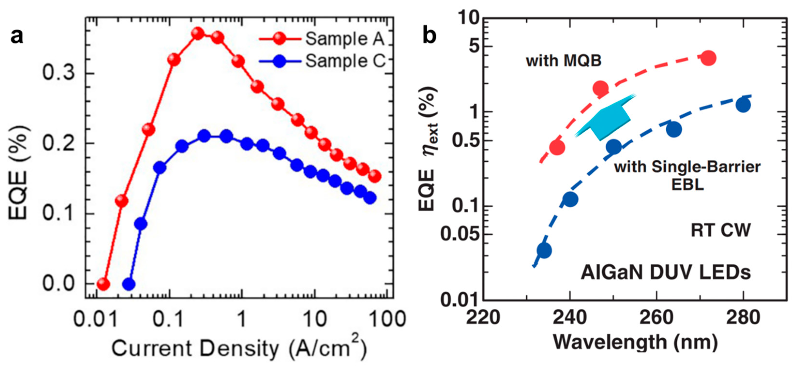
2. Advances in DUV-LEDs below 250 nm

On the whole, the performance level of sub-250 nm LEDs is much lower than that of the above-250 nm LED. The internal quantum efficiency (IQE), EQE, wall-plug efficiency (WPE), and light out-put power (LOP) have all dropped significantly. Up to now, the maximum EQE of 275 nm LED is 20.3% [13], the maximum EQE of 265 nm LED is 10% [14], while the majority of reported EQEs of sub-250 nm LEDs are below 1%. In 2006, Taniyasu et al. [15] obtained both n- and p-type AlN, and developed p-AlN/undoped AlN/n-AlN pin LED structure with n-AlN/AlGaN and p-AlN/AlGaN superlattices as the electron and hole lateral conduction layers, realizing emission at 210 nm. This is the first report of successful realization of AlGaN based 210 nm emission, confirming the possibility of full band coverage of AlGaN based LEDs. However, the device performance is extremely low, with the operation voltage of 45 V at 20 mA, LOP and EQE of 0.02 µW and 10−6% at 40 mA, respectively. In 2009, Hirayama et al. [16] fabricated an LED on a multilayer AlN buffer layer. They used a thin quantum well of 1.3–2 nm to suppress the polarization field in the well. At 100 mA, the peak wavelength located at 227 nm and the LOP and EQE were 0.15 mW and 0.2%, respectively. Next year, they [17] further improved the LED efficiency by introducing multi-quantum-barrier (MQB) electron blocking layers (EBL), providing an important scheme for preventing electron leakage of sub-250 nm LEDs. They achieved an LOP of 4.8 mW at 135 mA under CW operation for the 250 nm LED, corresponding to an EQE of 1.18%, which is still the highest EQE reported for 250 nm and sub-250 nm LEDs.
Recent years, the performance of sub-250 nm LEDs has been further improved. In 2020, Lobo-Ploch et al. [18] optimized the growth and fabrication processes including using epitaxially laterally overgrown (ELOG) sapphire substrates and vanadium-based low resistance n-contacts. They fabricated a 233 nm LED with an EQE of 0.36% at 100 mA. Recently, Jo et al. [19] demonstrated a 228 nm LED on sapphire substrates with an LOP of 1.4 mW at 150 mA by modifying the multiple quantum well (MQW) and spacer layer structures.
The method of using non-polar plane have also been explored [20]. Although the light extraction efficiency (LEE) was estimated to be 25 times higher than that on the polar plane, the EL intensity was approximately 70 times lower than that on the polar plane, which probably resulted from the higher defect density. New design concepts may break through the transparency and conductivity problem of sub-250 nm LEDs. Liu D. et al. [21] demonstrated a 229 nm LED adopting a p-type Si nanomembrane as both a p-contact and a hole injection layer. LOP was measured to be 0.16 mW under 100 mA current and EQE was calculated to be 0.03%. Next year, they demonstrated a 226 nm LED with a p-Si nanomembrane and achieved an EQE of 0.2% [22], which was the highest value among LEDs with emission wavelength below 230 nm in the CW mode.
Strong quantum-confinement GaN/AlN heterostructures can produce optical emission far above the bulk bandgap of GaN (3.4 eV), and offer another path to achieve DUV emission below 250 nm. Furthermore, it has been reported that delta-QW design could resolve the band-mixing issue and ensure large transverse electric (TE) spontaneous radiation rate [23]. S.M. Islam et al. [24] demonstrated that ultrathin (1–2 monolayers) GaN dots/disks embedded in an AlN matrix can achieve controllable emission in the 219–235 nm range, showing the shortest wavelength emission of 219 nm with an IQE of 40% from binary GaN active regions till date.
AlGaN based far-UVC LEDs grown by homogeneous epitaxy were also reported due to development of AlN single-crystal substrate. Toshio Nishida et al. [25] fabricated UV LED structures on AlN substrates as early as 2004, and compared the performance with LEDs on sapphire substrates. They found that the saturation injection current of LEDs on AlN substrate was two times higher than that of LEDs on sapphire substrate. This work confirmed the huge potential of bulk AlN substrates for UV-LEDs. In 2020, Yoshikawa et al. [26] reported the fabrication of 230–237 nm LEDs on AlN substrates. Thanks to the high-quality single crystal AlN substrate, the 233 nm LED exhibited EQE of 0.25% at 233 nm. Compared to sapphire and AlN substrates, Si substrate has several advantages [27], including low cost, good electrical and thermal conduction, and easy integration to Si-based electronics, etc. However, to obtain DUV LEDs on Si substrate has some problems that AlGaN epilayers grown on Si possess poor material quality owing to the large lattice and thermal mismatches between AlGaN and Si. The nanowire technology may solve the problem [28]. In 2015, S. Zhao et al. [29] achieved the first 210 nm emitting AlN nanowire LEDs with a turn on voltage of approximately 6 V by utilizing N-polar AlGaN nanowires directly grown on Si substrate. The IQE of the N-polar AlN nanowires LED can reach 80%.
Another important aspect of an LED are the reliability and lifetime. Lifetime in the order of 10,000 h for the long-wavelength UV LED (UVA and UVB) have been commercialized [30], while the lifetime for the long-wavelength UVC LED (>250 nm) is still limited to thousands of hours [31,32] although Ruschel et al. [31] demonstrated a 265 nm UVC LED with L70 lifetime more than 10,000 h. Meneghini et al. [33] pointed out that the stress induced nonradiative recombination increase and point defects in or around the active region might cause output power degradation. However, at present, there are few studies on the reliability and lifetime of sub-250 nm LEDs. The reported record lifetime of sub-250 nm LEDs was created by Yoshikawa et al. [26], which was expected to exceed 3600 h. The authors speculated that the possible reason for the long lifetime was the lower oxygen content in the novel structure. Glaab et al. [34], in detail, analyzed two possible degradation mechanisms of sub-250 nm LEDs. The first mechanism may be the activation of initially H-passivated defect complexes in or around the quantum well active region by hot carriers from Auger recombination, which may be responsible for the rapid decrease of LOP during the initial 50 to 100 h. The second mechanism may be the carrier injection efficiency reduction triggered by hot carriers from Auger recombination, which may be responsible for the LOP degradation after working more than 50 h.
The EQE, LOP and WPE of 250 nm and sub-250 nm LEDs are summarized in Figure 2a–c, respectively. Up to now, the research on AlGaN based sub-250 nm LED is still relatively few, compared to other UV wave bands. There are even no reports that demonstrated a WPE over 1%, implying a long way to realize large-scale commercial application. However, as it can been seen, the performance of recently reported sub-250 nm LEDs have increased by more than one magnitude over those reported several years ago, indicating the future of the commercialization of AlGaN based sub-250 nm LED is expectable.

3. Key Issues and Challenges

To analyze the key issues and challenges limiting the performance of AlGaN-based sub-250 nm LEDs, it is usually necessary to discuss from the two aspects of material growth and device physics. Generally, the technology roadmap of AlGaN-based sub-250 nm LEDs follows the ordinary UVC LEDs, which means the typical device structure and fabrication process of a sub-250 nm LED are basically identical to an UVC one. Figure 3a is a schematic diagram of the basic structure of an AlGaN-based UV LED. Typically, the epitaxial structure from bottom to top includes (1) substrate, generally sapphire or single crystal AlN, (2) AlN or AlGaN buffer layer, to reduce defects density and relax stress during growth, (3) n-AlGaN layer, to form n-type ohmic contact and provide electrons to active region for recombination, (4) active region, the main light emission region and usually made up of 3–5 periods of undoped AlxGa1−xN/AlyGa1−yN quantum wells (x < y), (5) EBL, with a wider bandgap than all other function layers to suppress the electrons to overflow to p-side, (6) p-AlGaN, to inject holes into active region for recombination, and (7) p-GaN cap layer, to form a p-type ohmic contact. From the perspective of materials, the bottom buffer layer quality that basically determines the upper epi-layer quality and the n/p doping efficiency that determine the carrier injection efficiency will significantly influence the device performance. Figure 3b is the schematic energy band structure of an AlGaN-based UV LED. The electrons and holes transport to the active region and recombine to each other to emit UV photons. If the carriers cannot effectively transport to the active region and be confined, the radiative recombination must be very weak. To say the least, even though the carrier recombination generates a large number of photons, the photons cannot be effectively extracted, and the device performance will be very low, too.
Quantitatively, if we choose the WPE as the key parameter to assess the performance of an LED, the relationship between the device performance and the main parameters can be expressed as the following Formula (1):
WPE = LOP I · V = EQE · EE = IQE · LEE · EE = RRE · CIE · LEE · EE
where I and V are the operation current and voltage, EE is the electrical efficiency, RRE is the radiative recombination efficiency, CIE is the carrier injection efficiency, respectively. The ABC model [38] is often used to estimate the RRE by the following Formula (2):
RRE = B n 2 A n + B n 2 + C n 3
where the coefficients A, B, and C represent the SRH non-radiative recombination coefficient (Shockley-Read-Hall, SRH), radiative recombination coefficient, and Auger recombination coefficient, and n is the carrier concentration, respectively. Apparently, the material crystal quality and carrier distribution will influence the performance through RRE, the doping efficiency and contact quality can mainly determine the performance through EE and CIE, and furthermore the LEE will directly determine the device performance. Consequently, the key issues and challenges including material crystal quality, n/p-type doping, carrier transport and confinement, and light extraction will be discussed in this part.

3.1. Material Crystal Quality

Guttmann et al. [10] have studied the reasons for the decrease of EQE at 264–220 nm. As shown in Figure 4a, with the wavelength decreasing, the trend of EQE is consistent with the trend of IQE, implying to improve the IQE becomes even more urgent for short wavelength range. As can be seen from the ABC model, IQE and non-radiative recombination process are inseparable. Due to the mismatch of lattice constants and thermal expansion coefficients between the AlGaN epilayer and substrates, dislocation density is generally high. Ban et al. [39] explored the relationship between IQE and dislocation densities (DDs) in the AlxGa1−xN/AlyGa1−yN active region with different Al compositions, and found that under the condition of the same dislocation density and injected carrier density, the active region has the same IQE regardless of the emission wavelength. The functional relationship between IQE and DDs is depicted in Figure 4b. It can be seen from the figure that the dislocation density needs to be less than 107 cm−2 to achieve an IQE of over 95%.
Before growing the LED structure, an AlN buffer layer is first grown on the sapphire substrate. The AlN buffer layer quality largely determines the quality of the upper LED structure. At the present stage, several technologies are commonly used to reduce dislocation density in the AlN/Sapphire template.
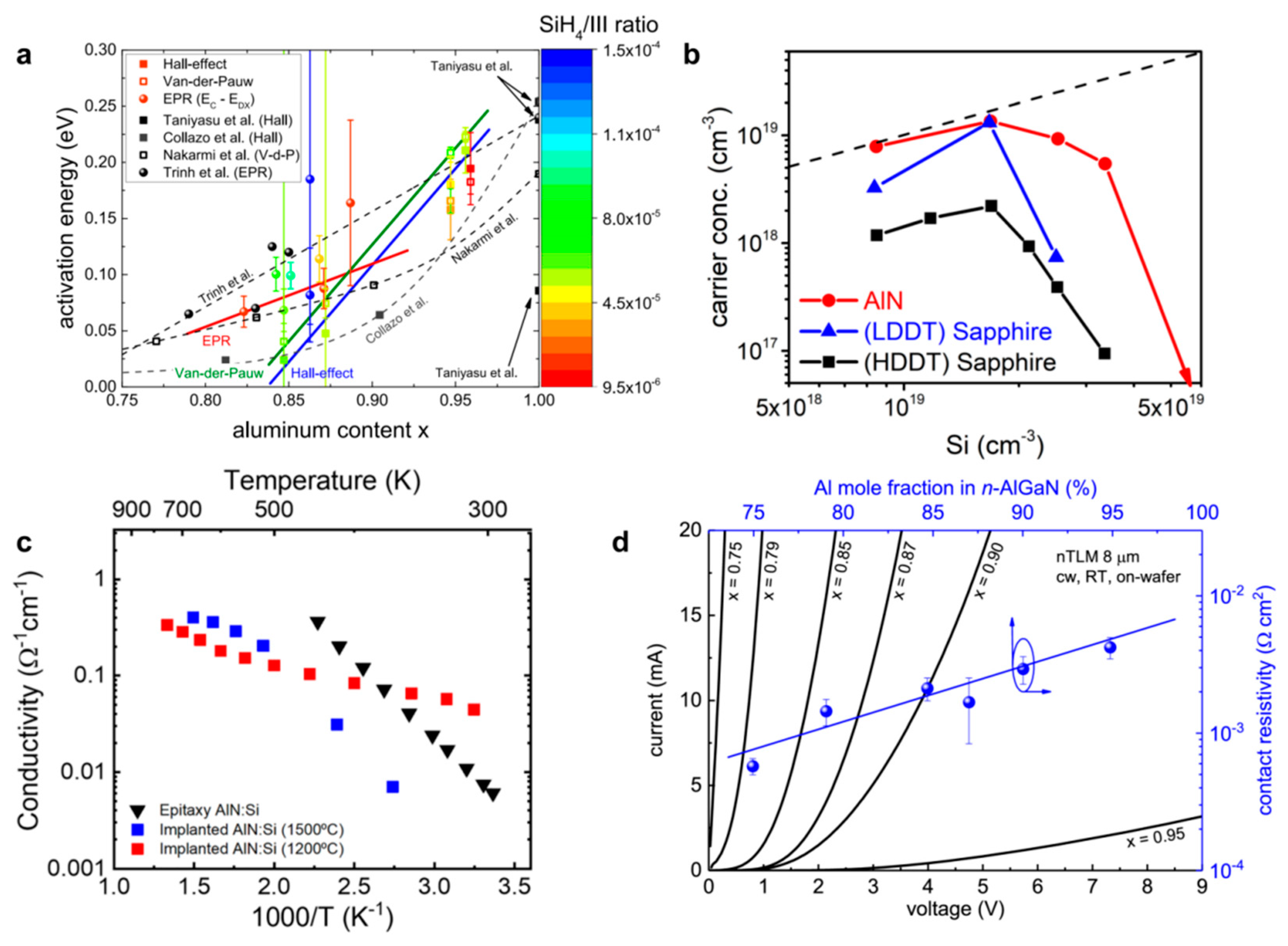
  • Two-step growth method [40,41,42,43]. It is used to alleviate the mismatch between AlN and sapphire substrate and improve the AlN quality. The first step is to form AlN crystal islands under high V/III ratio and low temperature. The second step is to grow AlN buffer layer with low threading dislocation density (TDD) and smooth surface through enhanced Al atom surface migration and lateral growth. The mechanism for reducing TDD is the transition from 3D to 2D growth mode that facilitates dislocation bending and annihilation along the growth direction. Hasan et al. [40] recently reported 4 um-thick AlN layers with total dislocation density of 1.1 × 109 cm2. Two-step growth exists the issue that the crystal islands may change their crystal orientation under the actions of airflow and rotation, etc., and thus generate threading screw dislocations. Three-step growth based on two-step growth was proposed [42]. The additional growth step is inserting a morphology control layer between the buffer layer and the step-flow-growth layer by adjusting the ammonia gas flow rate to a certain value. The twist angle of island could be controlled and the threading edge dislocation lines are more likely to form a loop and annihilate. The edge dislocation can drop to the order of 107 cm2;
  • Epitaxial lateral overgrowth (ELOG) method [44,45,46,47,48,49,50]. To be specific, the low DD is caused by filtration related to patterns on sapphire substrate and annihilation related to the formation of a loop structure during growth [47]. Nakano et al. [49] first demonstrated the ELOG-AlN layers on trenched-patterned sapphire substrates and achieved a dislocation density of 6.7 × 108 cm2. To further enhanced the coalescence of ELOG-AlN, Imura et al. [48] grew ELOG-AlN layers on patterned AlN templates grown on sapphire substrates and achieved a TDD value of less than 107 cm2. Recently, Liu et al. [50] proposed a preset strain modulation method on nano-patterned AlN templates by introducing HTA pretreatment. The XRC FWHM values of the (0002) and ( 10 1 ¯ 2 ) reflections were significantly dropped from 190 and 311 arcsec to 140 and 228 arcsec, respectively. At present, ELOG combined with HTA is believed to be the most effective approach for the growth of AlN layers in terms of crystal quality, cost and stability;
  • High-temperature annealing (HTA) of sputtered AlN on Sapphire [51,52,53,54,55,56]. Miyake et al. [55] first investigated the annealing of an AlN layer grown on a sapphire substrate and achieved a TDD of 4.7 × 108 cm−2. Annealing at temperatures above 1500 °C is effective in improving the quality of AlN layers. Due to the evolution mechanism of strains induced by HTA, it possesses high repeatability and stability and exhibits great potential in realizing mass production. The mechanism for reducing TDD after HTA was discussed in detail by Ben et al. [52]. Under TH, adjacent dislocations with different Burgers Vectors are more likely to form voids, which provide the inner surface for dislocations to terminate. The TDD below 107 cm−2 can be achieved through this method;
  • Migration-enhanced epitaxy (MEE) method [57,58,59,60,61]. MEE is achieved by alternative supply of the TMAl and NH3 sources. The Al atom migration can be enhanced and the gas phase reaction can be prevented in the meantime. When NH3 is not supplied, there are few N atoms on the epitaxial surface and the migration of Al atoms can be enhanced. Based on this route, NH3 pulsed-flow method and modified MEE were proposed [58,59,60]. Hirayama et al. [58] fabricated a high-quality AlN buffer by NH3 pulse-flow growth technique for the first time. The NH3 pulse-flow growth is realized by firstly injecting continuous TMAl flow during the NH3 pulse-flow sequence, secondly introducing continuous-flow mode to reduce the surface roughness, and then repeating the pulse- and continuous-flow modes. Li et al. [56] recently realized growing AlN layers under a relatively fast growth rate of 0.98 μm/h and achieved flat surface morphology (RMS = 0.5 nm) by NH3-pulse flow mode with a small duty ratio of NH3. A modified MEE is characterized by a combination of simultaneous source supply and conventional MEE, consisting of three different growth sequences including simultaneous, alternating supply and a combination of the two. Banal et al. [61] utilized the modified MEE to control the initial nucleation and achieved the XRC FWHM values of ~45 and ~250 arcsec for the (0002) and ( 10 1 ¯ 2 ) planes;
  • Interlayer method [62,63,64,65,66,67,68]. The inserting layers work by stress management and dislocation filter. Common insertion layers include medium-temperature (MT) interlayer [62,63,64,65], superlattices [66,67], graphene [68], etc. The introduction of a MT interlayer could lead to the formation of high-density self-organized nano-voids, which can alleviate tensile stress and reduce TDD due to promoting dislocation termination and bending at macrosteps at the same time. He et al. [64] recently successfully fabricated a 5.6 μm-thick AlN film by employing a MT interlayer (930 °C). The tensile stress in the AlN film had a reduction of 64% through this method and the TDD showed an extremely low value of 4.7 × 107 cm2. Wang et al. [66] grew high quality thick AlGaN on sapphire by inserting ten periods AlN (8 nm)/Al0.2Ga0.8N superlattices (SLs), and the TDD was reduced by two orders of magnitude.
For substrate selection, AlN single-crystal substrate is an ideal substrate for AlN and Al-rich AlGaN growth with low extended defect density and low non-radiative recombination centers [69,70,71]. The DD of AlGaN grown on AlN single crystal can be lower than 103 cm−2, which provides a significant progress for the application of ultrawide-bandgap AlGaN. However, with the development of ELOG and HTA technologies, the AlN template DD grown on sapphire substrate has reached very low magnitude of 108 cm2 [48], allowing the better performance of sub-250 nm LEDs grown on cost-effective sapphire substrate. Although, at present, the DD of LEDs grown on sapphire substrates is four orders of magnitude larger than that of LEDs grown on single-crystal AlN, the EQE of sub-250 nm LEDs grown on sapphire are similar to those grown on single-crystal AlN [18].

3.2. n-AlGaN with High Al Composition

The contact resistivity and sheet resistivity of the n-AlGaN layer, which influence the electron injection efficiency, are depended on the Si doping efficiency. The ionization energy (Ea) of Si is approximately 15 meV when Al composition is smaller than 80% [72], therefore the free electron concentration can achieve the order of 1019 cm−3 and the contact resistance and sheet resistance are within acceptable ranges. However, when the Al content is higher than 80% which is essential for sub-250 nm LED, Si doping faces severe difficulties. First, the Si Ea sharply increases with Al composition and can reached to 250 meV in AlN [72,73], as shown in Figure 5a. In principle, Ea can be reduced by increasing the doping concentration to form impurity bands, yet self-compensation effect will reduce the free electron concentration when the Si doping concentration exceeds the critical doping dose, and the conductivity of the film will drop drastically, which is called a “knee behavior” [74], as shown in Figure 5b. Furthermore, it has been reported that the rapid decrease in conductivity also correlates with the transformation of Si from shallow donor to DX center [74]. The name of DX center derives from the fact that it is originally thought to be a deep donor (D) level associated with an unknown impurity (X) [75]. It is a highly localized center of negative charge related to two donor atoms, whose generation can be described by a chemical-like Equation (3)
2 d 0 D X + d +
where d0 and d+ represent neutral and ionized substituted shallow donor atoms, respectively. The DX centers are thought to resulting from the breaking and displacement of covalent bonds of Si atoms and nearest neighbor metal atoms in wurtzite crystals.
Low self-compensation can be achieved via VAl-nSiAl complexes by defect quasi-Fermi level control (dQFL), chemical potential control (CPC), and the optimization of growth conditions including reactor pressure and temperature, etc. [76,77,78]. Non-equilibrium process such as Si implantation can inhibit the formation of DX centers, providing higher free carrier concentrations. In 2020, Breckenridge et al. [79] implanted Si into homoepitaxial AlN and performed a low thermal budget damage recovery and activation process, achieving an n-AlN with conductivity of 0.05 Ω−1·cm−1 at room temperature, as shown in Figure 5c. Later, in 2021, Breckenridge et al. [76] further realized Si-implanted n-AlN with higher conductivity (>1 Ω−1·cm−1) and carrier concentration (5 × 1018 cm−3) on low TDD AlN substrate, maintaining the Si dopant in a shallow state via a non-equilibrium annealing process and dQFL control method.
For the purpose of enhancing the WPE, the contact resistivity of the n-electrode must be reduced. However, the n-type ohmic contact with high Al composition faces with physical limitations that the electron affinity of AlGaN decreases from 3.18 eV for GaN to 1.01 eV for AlN [80], giving rise to the Schottky barrier increase at the metal semiconductor (MS) interface with Al content. Figure 5d summarized the electrical characteristics of n-contacts by carefully optimizing the annealing conditions on n-AlGaN with Al content from 0.75 to 0.95 [81]. At present, suitable low work function metals have not been found. However, vanadium can form thermal stable nitrides with low work functions and is considered as an alternative metal to Ti. When Al mole fraction is greater than 0.6, the common Ti/Al-based n-electrode should be replaced by V/Al-based contacts [82]. Moe et al. [35] adopted Ti/Al/Ni/Au on n-Al0.87Ga0.13N as the n-electrode and fabricated an LED with emission wavelength of 233 nm. The device had an operation voltage of 10.4 V at 100 mA. Sulmoni et al. [80] used V/Al-based n-type contacts on n-Al0.87Ga0.13N and fabricated an LED. The operation voltage was 9.9 V at 100 mA. In addition, Nagata et al. [83] reported that a thin SiNx interlayer can reduce the n-type contact resistivity by more than one order of magnitude in the Al mole fraction range from 0.62 to 0.87.
Figure 5. (a) The dependence of Si Ea on Al composition [73]. (b) The conductivity of n-AlGaN on different substrate with increasing Si doping concentration [74]. (c) Temperature dependent conductivity for the epitaxially doped AlN film, the Si-implanted AlN film on sapphire, and the Si-implanted AlN film on AlN substrate [79]. (d) IV curves and contact resistivity for n-contacts on n-AlGaN as a function of Al mole fraction [81].
Crystals 12 01812 g005

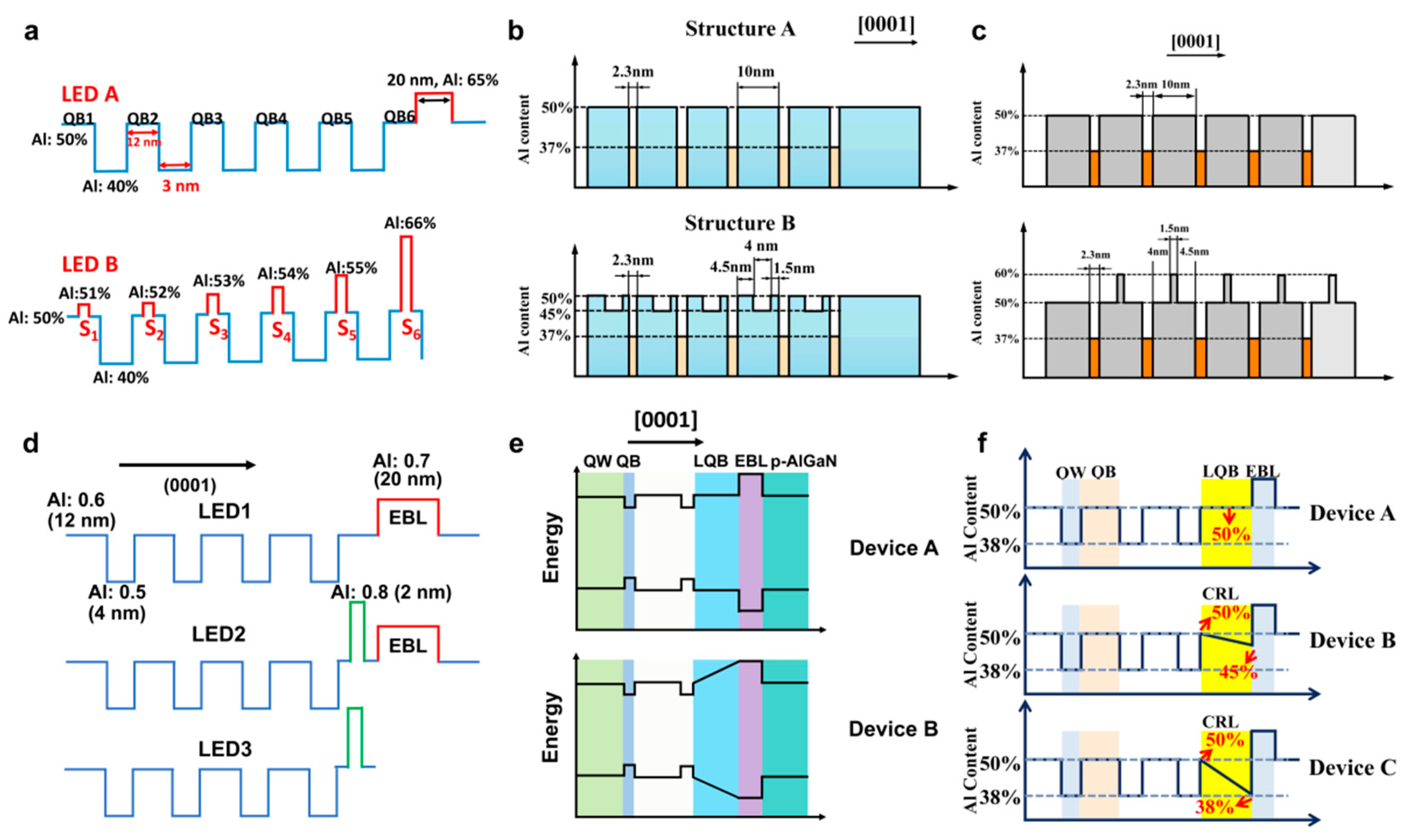
3.3. Carrier Confinement and Transport

Driven by the external electric field, electrons and holes transport through the device by means of tunnelling or diffusion. Insufficient hole injection and electron leakage are the common problems during carrier transport in III-nitride based LEDs. In the review by Li et al. [84], methods of improving hole injection were explained and summarized in detail. The reason why electrons have difficulties in being restricted to the active region is that, the p-type layers cannot provide sufficient holes, and the hole mobility is low due to its large effective mass, resulting in asymmetric electron and hole injection [63]. To make matters worse, when emission wavelengths is smaller than 250 nm, the Al compositions of quantum wells and barriers become higher and higher, and the conduction band offset from the active region to the EBL becomes smaller and smaller. The severe electron leakage makes the electron injection efficiency quite low (<20%) [85]. Electron leakage has become one of the most severe problems for the sub-250 nm LEDs. A. Pandey et al. [36] measured the EQE of 245 nm LEDs with different EBL designs, and observed severe efficiency droop at 0.25 A/cm2, as shown in Figure 6a. Their studies suggested that the observed efficiency droop is largely due to an electrical effect instead of an optical phenomenon.
An effective solution for the severe electron overflow is to introduce a MQB EBL, which can cause multiple reflection effects and increase the effective barrier height. In 1986, Iga et al. [86] theoretically compared the MQB and the traditional single barrier EBL, and the results showed that the thickness modulated MQB EBL increased the effective electron barrier height by two times. In a report by Hirayama et al. [17] in 2010, MQB was introduced into UVC LEDs as the EBL. The EQE and LOP of the 250 nm-LED with MQB EBL reached 1.18% and 4.8 mW, respectively, which was 2.7 times increased compared to that with single barrier EBL. Figure 6b summarizes the wavelength dependent EQE with MQB and single barrier EBLs, proving the significant enhancement of carrier confinement by using MQB EBL. The influences of EBL thickness and doping on the hole injection and electron blocking effect in sub-250 nm LEDs was also explored. It was shown that EBL without doping could greatly suppress the parasitic emission peaks generated by the surface Mg-related deep level transition, and thickening the EBL could increase the radiative recombination [64]. Other methods to improve hole injection and electron confinement by optimizing EBL have been extensively studied such as wideband gap interlayer and Al composition-graded EBL [87,88]. Concerning that it was still difficult to achieve high quality AlGaN epitaxial layer and high Mg doping concentration with high Al content, Kuo et al. [89] adopted Al0.55Ga0.45N/Al0.75Ga0.25N SLs EBL to replace Al0.85Ga0.15N single barrier EBL. The WPE and LOP were almost the same.
To optimize the quantum barrier (QB) in the active region is also important to improve the carrier confinement and transport efficiency. Velpula et al. [90] inserted a thin AlGaN layer with higher Al content into each QB in the active region, as shown in Figure 7a, and the electron leakage was reduced by approximately 11 times and LOP was increased by approximately 225% at 60 mA compared to the reference LED structure. Lang et al. [91] applied an asymmetric concave QB by inserting an AlGaN layer with lower Al content into the QB, forming a concave region on the energy band, as shown in Figure 7b. This structure can enhance the electron capture ability of QWs, accelerate the hole transport under polarization induced field, and enhance the hole vertical transport. The maximum EQE was 2.32 times higher than that of the reference one. The QB band modulation can also be achieved by inserting a thin layer with high Al content [92], as shown in Figure 7c. By the energy band modulation effect of the delta-AlGaN layer, holes can be accelerated and cross the high barriers with very large kinetic energy, thus enhancing the hole injection into the active region. The maximum EQE is 1.6 times higher than that of the reference one.
There are also many optimizations within the last quantum barrier (LQB) near the EBL, such as the insertion of a thin undoped AlGaN strip layer in the middle of the LQB and Al composition-graded LQB [93,94,95]. Figure 7d–f exhibits schematic conduction band diagrams of different optimizations within the LQB. It is worth mentioning that composition-graded LQB has two kinds of variations, namely increasing and decreasing [94,95], and specific choice need to be optimized according to the material and structure. In addition, although EBL can suppress electron leakage, the hole injection efficiency is still greatly affected due to the formation of positive polarization surface charge between the LQB and EBL [93,96]. To solve this problem, EBL-free structure was also proposed. Simulation analysis by Shi et al. [97] showed that utilizing Al composition-graded AlGaN insertion layer and EBL-free structure could effectively block electrons and improve hole injection efficiency. The IQE was increased by 64.3% compared to the reference device with EBL.
Although these energy band and carrier velocity modulation methods within EBL and active region are mainly applied in above-250 nm LEDs, we believe they also have great application potential in sub-250 nm LEDs.

3.4. p-AlGaN with High Al Composition

It is observed that the Mg doping efficiency in AlGaN decreases dramatically with increasing Al mole fraction [98,99]. To achieve high-efficiency p-doped AlGaN has become one of the key issues limiting the development of sub-250 nm LEDs. The low p-doping efficiency of AlGaN is mainly caused by three reasons.
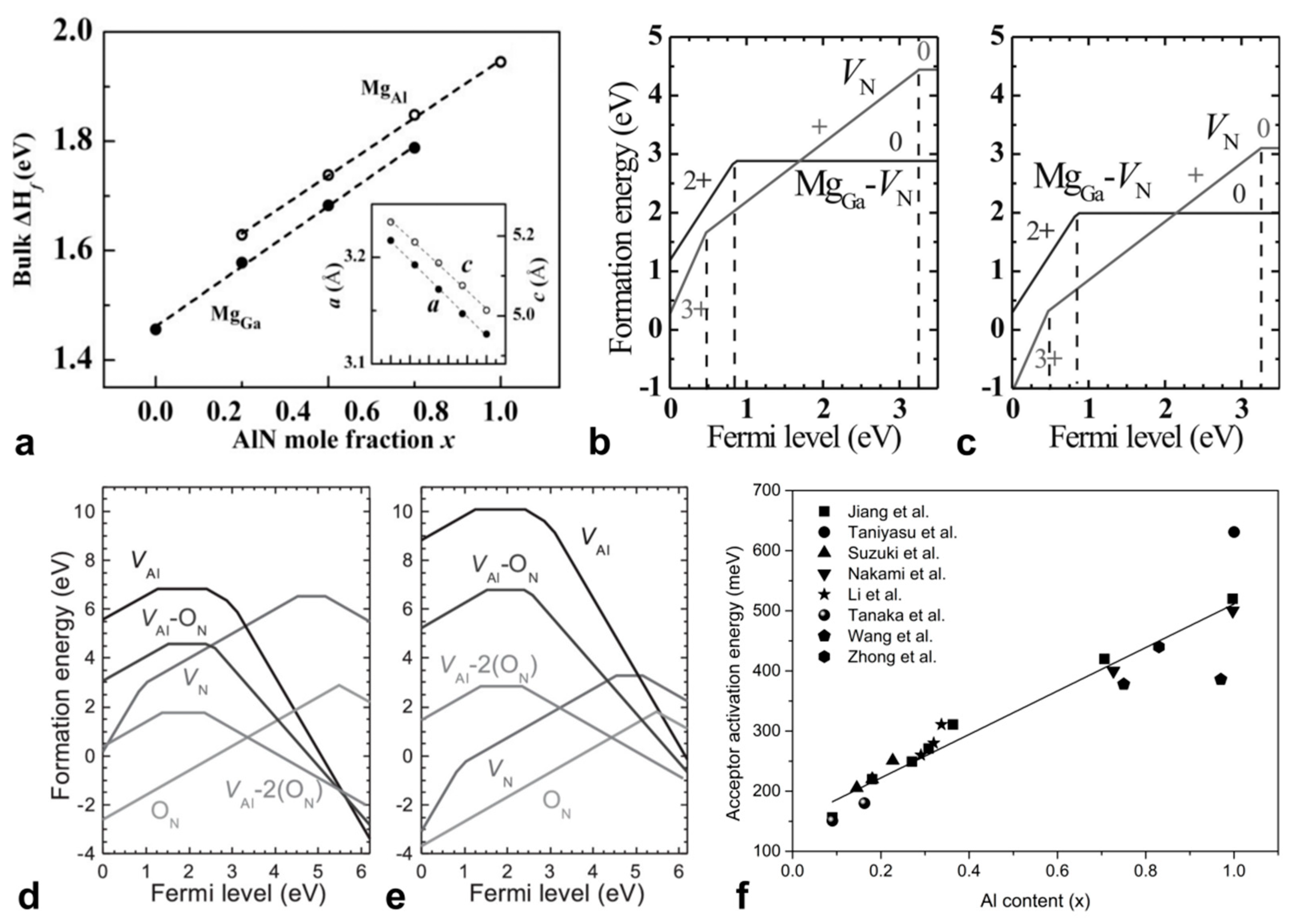
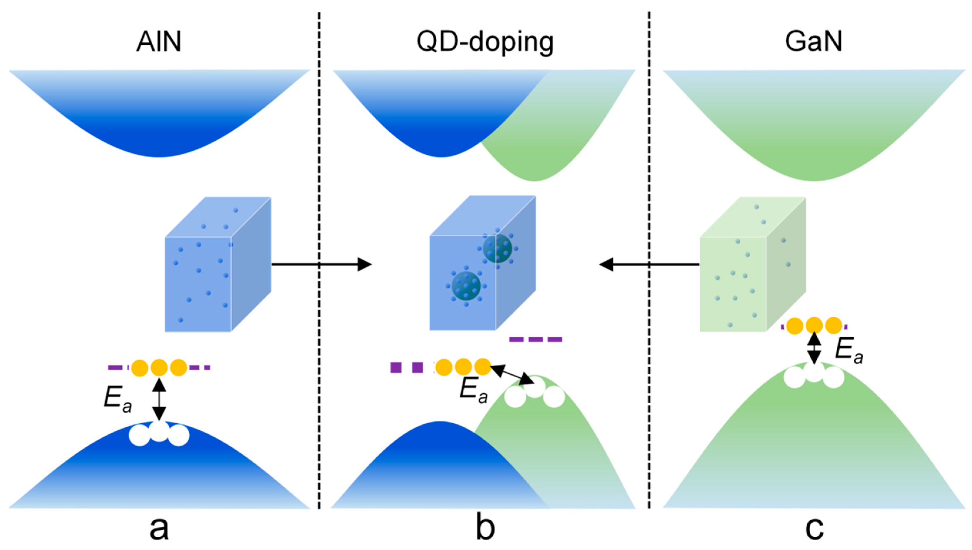
  • The solubility of Mg in GaN and AlN is low. The solubility of Mg replacing Ga or Al atoms in AlGaN is limited by the positive formation enthalpies. The influence of formation enthalpies on the solubility of Mg can be expressed as the following Equation (4)
    C Mg = N · e x p ( Δ H f k T )
    where CMg is the solubility of Mg atoms, N is the number of lattice points which can be occupied by the doping atoms, Δ H f is enthalpy change, k is the Boltzmann constant, and T is the temperature. As shown in Figure 8a [100], as the Al content in AlxGa1−xN increases, both the MgAl and MgGa formation enthalpies monotonically increase, indicating limited Mg solubility;
  • Self-compensation of intrinsic defects [101]. Figure 8b–e show the formation energies as a function of Fermi level for different defects in GaN and AlN [102,103]. The compensation of VN is an important mechanism resulting in hole concentration decreasing. VN can provide one, two, or three electrons, and only the charge states of V N + and V N 3 + are stable. Since V N 3 + has smaller formation energy than V N + , V N 3 + is believed to be the main compensating defects in Mg-doped AlGaN alloys [104]. Stampfl et al. [101] found that VN was more easily formed in AlN than in GaN. The compensation of natural defects requires to be controlled especially in Al-rich AlGaN alloys;
  • The acceptor Ea is very high and gradually increase with Al content, as shown in Figure 8f [105,106]. Mg is generally used as the p-type dopant in AlGaN epilayer. The Ea of Mg in p-GaN films is in the range from 120 to 200 meV, generating a hole concentration of 1017–1018 cm−3 [107]. However, when the Al content changes from 0 to 100%, the Ea of Mg increases from 160 meV to over 500 meV [99,105]. The hole concentration (p) in wide-bandgap semiconductors can be estimated by the following Formula (5) [108]
    p = 1 g N A · N V · e x p ( E a 2 k T )
    where g is the acceptor degeneracy (g = 2), NA is the acceptor concentration, and NV is the effective state density near the valence band maximum (VBM). It can be seen that the increase of Mg acceptor Ea makes the hole concentration exponentially decrease, leading to the decrease of conductivity.
Figure 8. (a) Formation enthalpies of MgGa/MgAl in the bulk AlGaN as a function of Al content under N-rich condition [100]. Formation energies as a function of Fermi level for the VN and the MgGa–VN complex in GaN, under (b) N-rich and (c) Ga-rich conditions [102]. Formation energies as a function of Fermi level for the VN, VAl, ON, VAl−ON and VAl−2(ON) in AlN, under (d) N-rich and (e) Al-rich conditions [103]. (f) The activation energy of Mg in AlxGa1−xN in dependence of Al mole fraction x, data extracted from [105,106].
Crystals 12 01812 g008
The surface during epitaxy plays an important role in determining the solubility of the dopant. Tersoff [109] pointed that the elastic interaction of the dopants with the surface relieved the stress caused by atomic size mismatch and lowered the impurity energy owing to the coupling of the impurity stress to the spatially surface stress, thus the solubility of dopants could be significantly improved. Zheng et al. [100] proposed a modified surface engineering technique (MSE) by periodic interruptions under an ultimate V/III ratio condition to enhance Mg effective incorporation without affecting the growth of AlGaN films. Schematic diagram of the Mg incorporation behavior in the AlGaN is shown in Figure 9. For Al0.99Ga0.01N, the final doping concentration of Mg can reach 5 × 1019 cm−3.
Self-compensation by VN complexes can be suppressed by elevating V/III ratio during growth [71,99,104] and defect quasi Fermi level (dQFL) method [110]. Nakarmi et al. [104] increased the V/III ratio up to 5000 in the growth of the p-type Al0.7Ga0.3N with a Mg concentration of 1020 cm−3 and significantly suppressed the related transition, while T. Kinoshita et al. [99] increased the V/III ratio to 1800 with a Mg concentration of 1019 cm−3 and achieved a low resistivity of 47 Ω·cm for Al0.7Ga0.3N. The discrepancy of the V/III ratio might result from larger formation energy of VN3+ and higher crystalline quality under lower Mg concentration [99]. dQFL method utilizes illumination during growth to increase the formation energy of the compensating point defects. A. Klump et al. [110] observed the reduction of VN-related emission for the dQFL-process samples, and validated the effectiveness of dQFL control process in point defect management for Mg-doped III-nitride films.
To reduce the acceptor Ea for AlGaN with high Al composition, several methods were developed in recent two decades. Under the condition of heavy doping (>2 × 1019 cm−3), the hole concentration provided by the impurity band is two orders of magnitude larger than the valence band transport, exhibiting very low acceptor Ea. In addition to forming impurity band, the Mg acceptor Ea can be reduced by Mg pulse or δ-doping [111,112,113,114,115,116,117,118]. δ-doping had been proved to effectively increase the hole concentration without causing a crystal quality droop [119]. The polarization-induced doping [120,121,122] and superlattice doping [123,124,125] are two common-used methods to reduce the apparent acceptor Ea. Under biaxial strain, AlGaN layers will generate huge polarization induced electric field (105–107 V/cm), making the valence and conduction bands tilt, thereby the acceptors ionization probability gets larger. Under polarization-induced electric field, free holes will be swept to the interface, generating two-dimensional hole gas (2DHG) near the interface, and simultaneously generating a depletion layer. If the thickness of the depletion layer is too thick, the vertical transport of holes will be hindered. Thus, the thickness of the thin layer should be limited to 0.6–10 nm [126]. To avoid the free carrier accumulation at the interface, three-dimensional polarization doping was adopted by means of gradually changing Al content, which could generate three-dimensional hole gas (3DHG) [122,127]. SLs doping can reduce the Ea via modulating the band structure based on spontaneous and piezoelectric fields. Kazuaki Ebata et al. [128] achieved high hole concentrations on the order of 1018 cm−3 and small Ea of 40–67 meV by adopting AlN/Al0.75Ga0.25N SLs with an average Al composition of 0.8. As one kind of SLs doping methods, short-period superlattice (SPSL) is very effective to improve p-doping efficiency [123,129]. Schubert et al. [107] made a theoretical analysis and found that for SPSL (<100 Å) doping, the free carrier concentration could increase by more than ten times when the magnitude of the valance band modulation and the Mg Ea were equal. Wang et al. [130] proposed a desorption-tailoring method and remarkably reduced the Mg Ea to 17.5 meV in p-AlGaN SLs with an average Al composition of 51%. The desorption process, achieved by interrupting the supply of the precursors, was the reverse process of absorption of atoms to the surface. Specified SLs can be grown by adjusting the desorption time and matching the desorption time and epitaxy time. Based on the reduction of activation energy and enhancement of Mg surface-incorporation, the hole concentration in SLs reached 8.1 × 1018 cm−3 at room temperature.
Recently, K. Jiang et al. [106] proposed a new method to improve the doping efficiency called “quantum engineering of non-equilibrium p-doping” in which the key points were, firstly, embedding relatively narrow bandgap quantum structure into wide bandgap matrix to produce a new band edge, and secondly, enriching the Mg dopants near the interfaces to improve ionization, as shown in Figure 10. The Mg Ea of AlGaN with Al content of 50~70% was reduced to below 50 meV, and the hole concentration reached higher than 1018 cm−3 at room temperature.
Although the Mg acceptor Ea in AlGaN with high Al content can be reduced to even lower than that in GaN by various designs, the resistivity is still relatively higher due to significantly reduced hole mobility. Maybe, to increase the hole mobility is the next breakthrough of p-type doping for Al-rich AlGaN.

3.5. Light Extraction

According to the current researches, the low LEE may be the most serious problem hindering the UV LED performance, especially for sub-250 nm LEDs. The two main factors restricting the LEE are: (a) the balance between increasing transparency and decreasing driving voltage; (b) the transformation of emission light polarization from TE to transverse magnetic (TM) mode. For instance, to realize 240 nm transparency, the Al content larger than 80% is required within the LED structure. When the emission wavelength is 222 nm, Al mole fraction should be as high as 0.95 to ensure totally transparent, which greatly increases the operation voltage. Hence, a careful trade-off between reducing the optical absorption and increasing the conductivity is needed to achieve relatively high WPE. Furthermore, when the emission wavelength reduces to below 250 nm, the increase of Al mole fraction leads to the rearrangement of valence bands. The main polarization mode of the emission light shifts from TE, which mainly propagates along the (0001) direction that usually vertical to the device surface, to TM mode, which mainly propagates laterally in the c-plane that usually parallel to the device surface [10,131,132]. It was reported that the optical extraction efficiency of TM mode is less than 1/10 that of TE mode [133].
Self light absorption is a severe problem for all UV LEDs and schemes for boost transparency in other UV wavebands can also be applied to sub-250 nm LEDs. The reduction of light absorption can be achieved by using a transparent p-AlGaN contact layer [15,134,135], a highly reflective electrode structure, photonic crystal (PhC) and other reflection structures [13,136,137,138], etc. Mg-doped AlxGa1−xN/AlyGa1−yN SPSL can provide transparent p-type contacts, yet the turn-on voltage is still high due to the high vertical resistivity and low mobility of the free carriers [15]. Muhin et al. [134] investigated the vertical conductivity of Al0.71Ga0.29N/Al0.65Ga0.35N:Mg SPSLs and observed that its value was strongly affected by temperature and electric field, to be specific, the vertical conductivity could increase by almost two orders of magnitude when the electric field varied from 0.05 to 0.98 MV·cm−1, or the temperature increased from room temperature to 100 °C. Guttmann et al. [135] showed that the average Al mole fraction should be high enough to be transparent for emission wavelength, and a five-fold increase of the on-wafer EQE could be achieved combined with reflective In p-contacts. Kashima et al. [138] improved the EQE of 283 nm LED from 4.8% to 10% by introducing high-reflectance PhC and reflective Ni/Mg p-electrodes on the surface of the contact layer as shown in Figure 11a. Takano et al. [13] reported a 275 nm LED with an EQE of 20.3% by combining various ways to improve the LEE, including the adoption of transparent AlGaN:Mg contact layer and Rh mirror electrode. When reflective p-electrodes were used, EQE could be significantly improved by optimizing the thickness of p-type layers [139]. As shown in Figure 11b, there are two light paths: directly from the active region toward the sapphire (solid arrow) and reflected by the p-electrode toward the sapphire (dashed arrow). When the total optical thickness of the p-type layers changes, the optical path difference between the two paths changes, creating interference and significantly affecting the LOP.
Since the DUV transparent AlGaN:Mg contact layer will lead to the low efficiency of hole injection, it is feasible to utilize the polarization field and tunnel junction. As shown in Figure 11c, the tunnel junction is a p-n junction working at reverse bias, which can achieve high reverse current through interband tunnelling at low reverse bias. In early works, the formation of an effective tunnel junction usually required degenerate p- and n-doping to achieve very narrow depletion regions, so that the carriers could easily tunnel from valance band on one side to conduction band on the other side. Whereas, degenerate p-type doping was almost impossible to achieve in high Al content AlGaN, researchers proposed a tunnel junction based on heterointerface polarization charges, which could eliminate the need for heavy doping [140]. Recently, Mehnke et al. [141] fabricated a tunnel heterojunction LED with an emission wavelength of 232 nm. The LOP and EQE reached to 1.73 mW and 0.35% at 100 mA under pulsed operation, respectively. However, the operation voltage (26 V at 10 mA) was still high compared to the reference traditional LED (6.8 V at 10 mA). The doping of the tunnel junction interface should be optimized to reduce the resistance and operation voltage.
Under the crystal field and spin-orbit coupling, the valence band for wurtzite AlGaN materials contains heavy hole (HH), light hole (LH), and crystal field splitting hole (CH) sub-bands. The emitting light polarization is determined by the valence sub-band distribution. The topmost CH and HH sub-bands will lead to TM- and TE-dominated emission, respectively. The critical Al mole fraction triggering the transition from TE mode to TM mode depends on the strain state and quantum confinement [142], as shown in Figure 12a. Under compressive strain, the HH and LH sub-bands will be lifted up, while the CH subband will be pulled down, resulting TE mode enhancement. Enhancing the quantum confinement will greatly pull down the CH sub-band due to its light effective mass, even resulting in the intersection to LH and HH and also promoting the TE mode. The QW width and barrier height can affect the quantum confinement, thus controlling the polarization mode. Figure 12b shows that when the QW is relatively thick (>3 nm), the critical Al mole fraction is independent of the QW width. When the QW is relatively thin (<3 nm), the thinner the QW gets, the higher the critical Al mole fraction gets [142]. Figure 12c displays the calculated degree of polarization (DOP, I T E I T M I T E + I T M ) by k·p theory of an AlGaN QW with different well and barrier Al contents pseudomorphically grown on AlN bulk substrate with thickness of 1.5 nm [143]. As it can be seen, for a certain well Al content, increasing the barrier Al content can improve the DOP, for a certain barrier Al content, decreasing the well Al content can improve the DOP, and for a certain emission wavelength such as 230 nm, it is necessary to simultaneously increase the barrier Al content and decrease the well Al content.
Experimentally, when the QW is under strain free or compressive strain states, the TE emission and quantum efficiency will be greatly improved [144,145,146]. ELOG for reducing TDD can also enhance TE mode emission due to the differences in thermal expansion coefficients. In 2021, Zhang et al. [147] successfully modulated the strain state of AlN template by adopting multiple alternation cycles of low- and high-temperature growth. Hence, the in-plane compressive strain of the QWs had increased. The DOP was enhanced from 41.5% to 61.9%. When the GaN quantum well width is reduced to a few atom monolayers (MLs), strong quantum confinement will appear, which can increase the effective transition energy of GaN by several eV. Some groups [23,24,148,149] have carried out related studies on AlN-delta-GaN QW LEDs and achieved lower wavelength emission. The advantage of this method is that in addition to increasing TE emission, the spontaneous emission rate is also significantly increased by suppressing the QCSE. At present, researches on AlN-delta-GaN QW LEDs are still in the early stage, further and deeper researches need to be carried out and its feasibility requires to be confirmed.

4. Conclusions and Prospect

Nowadays, the technology roadmap of AlGaN based sub-250 nm LEDs is basically similar to the conventional DUV LEDs. The performance collapse mainly results from the problem accumulation with Al composition increasing of each layer in the device structure. First of all, improving the material crystal quality is the key issue to promote the sub-250 nm LED performance. Before the AlN single-crystal substrate fabrication and homogeneous epitaxy technologies mature, the AlN/Sapphire template is still the best choice. HTA is a promising method, which can provide cost-effective, stable, high-quality, and compressive strain AlN/Sapphire, benefiting the IQE and LEE.
The contact and sheet resistivity of the n-AlGaN layer contribute part of the driving voltage. When Al mole fraction is larger than 0.8, shallow donor Si gradually changes into a deeper donor, and finally becomes a stable charge capture center, leading to a significant increase in resistivity. Controlling the formation of DX centers is a critical technical challenge for high Al composition AlGaN. Optimization of n-layers, including modulating growth conditions and searching for suitable contact metals, need to be further explored. For carrier confinement and transport, although a large number of energy band engineering studies have been carried out to enhance carrier confinement, electron overflow is still one of the most severe problems in sub-250 nm LEDs due to the physic limitations. The MQB EBL is a promising method to increase the effective electron barrier.
Resulting from the increase Ea of Mg dopants in AlGaN, p-AlGaN layers cannot offer sufficient free carriers and enough high conductance. Different methods, such as δ-doping, quantum engineering doping, polarization induced doping, and superlattice doping, etc., have been proposed to improve the doping efficiency, while it is still facing daunting challenges. In addition, how to increase the hole mobility may be the next problem to be solved. Serious light absorption and emission mode transition problem greatly reduces the LEE in this wavelength range. Adopting tunnel junction may be a quite hopeful method to achieve fully transparent LED.

Author Contributions

Conceptualization, K.J., X.S. and D.L.; methodology, K.J. and C.Z.; writing—original draft preparation, C.Z.; writing—review and editing, K.J.; project administration, K.J., X.S. and D.L.; funding acquisition, K.J., X.S. and D.L. All authors have read and agreed to the published version of the manuscript.

Funding

This research was funded by National Key R&D Program of China (grant number 2022YFB3605103); National Natural Science Foundation of China (grant numbers 62004196, U22A2084, 62121005, and 61827813); Youth Innovation Promotion Association of Chinese Academy of Sciences; and Youth Talent Promotion Project of the Chinese Institute of Electronics (grant number 2020QNRC001).

Data Availability Statement

Not applicable.

Conflicts of Interest

The authors declare no conflict of interest.

References

  1. Zollner, C.J.; DenBaars, S.P.; Speck, J.S.; Nakamura, S. Germicidal ultraviolet LEDs: A review of applications and semiconductor technologies. Semicond. Sci. Technol. 2021, 36, 123001. [Google Scholar] [CrossRef]
  2. Mehnke, F.; Guttmann, M.; Enslin, J.; Kuhn, C.; Reich, C.; Jordan, J.; Kapanke, S.; Knauer, A.; Lapeyrade, M.; Zeimer, U.; et al. Gas Sensing of Nitrogen Oxide Utilizing Spectrally Pure Deep UV LEDs. IEEE J. Sel. Top. Quantum Electron. 2017, 23, 29–36. [Google Scholar] [CrossRef]
  3. Mellqvist, J.M.; Rosén, A. DOAS for flue gas monitoring—I. Temperature effects in the U.V./visible absorption spectra of NO, NO2, SO2 and NH3. J. Quant. Spectrosc. Radiat. Transf. 1996, 56, 187–208. [Google Scholar] [CrossRef] [Green Version]
  4. Hodgkinson, J.; Tatam, R.P. Optical gas sensing: A review. Meas. Sci. Technol. 2012, 24, 012004. [Google Scholar] [CrossRef] [Green Version]
  5. Xu, Z.; Sadler, B.M. Ultraviolet Communications: Potential and State-Of-The-Art. IEEE Commun. Mag. 2008, 46, 67–73. [Google Scholar]
  6. Sun, K.X.; Allard, B.; Buchman, S.; Williams, S.; Byer, R.L. LED deep UV source for charge management of gravitational reference sensors. Class. Quantum Gravity 2006, 23, S141–S150. [Google Scholar] [CrossRef]
  7. Narita, K.; Asano, K.; Morimoto, Y.; Igarashi, T.; Hamblin, M.R.; Dai, T.; Nakane, A. Disinfection and healing effects of 222-nm UVC light on methicillin-resistant Staphylococcus aureus infection in mouse wounds. J. Photochem. Photobiol. B Biol. 2018, 178, 10–18. [Google Scholar] [CrossRef]
  8. Zwicker, P.; Schleusener, J.; Lohan, S.B.; Busch, L.; Sicher, C.; Einfeldt, S.; Kneissl, M.; Kühl, A.A.; Keck, C.M.; Witzel, C.; et al. Application of 233 nm far-UVC LEDs for eradication of MRSA and MSSA and risk assessment on skin models. Sci. Rep. 2022, 12, 2587. [Google Scholar] [CrossRef]
  9. Guttmann, M.; Lobo-Ploch, N.; Gundlach, H.; Mehnke, F.; Sulmoni, L.; Wernicke, T.; Cho, H.K.; Hilbrich, K.; Külberg, A.; Friedler, M.; et al. Spectrally pure far-UVC emission from AlGaN-based LEDs with dielectric band pass filters. J. Phys. D Appl. Phys. 2022, 55, 205105. [Google Scholar] [CrossRef]
  10. Guttmann, M.; Mehnke, F.; Belde, B.; Wolf, F.; Reich, C.; Sulmoni, L.; Wernicke, T.; Kneissl, M. Optical light polarization and light extraction efficiency of AlGaN-based LEDs emitting between 264 and 220 nm. Jpn. J. Appl. Phys. 2019, 58, SCCB20. [Google Scholar] [CrossRef]
  11. Mehnke, F.; Sulmoni, L.; Guttmann, M.; Wernicke, T.; Kneissl, M. Influence of light absorption on the performance characteristics of UV LEDs with emission between 239 and 217 nm. Appl. Phys. Express 2019, 12, 012008. [Google Scholar] [CrossRef]
  12. Kneissl, M.; Rass, J. III-Nitride Ultraviolet Emitters: Technology and Applications, 1st ed.; Springer: Berlin, Germany, 2016; pp. 90–92. [Google Scholar]
  13. Takano, T.; Mino, T.; Sakai, J.; Noguchi, N.; Tsubaki, K.; Hirayama, H. Deep-ultraviolet light-emitting diodes with external quantum efficiency higher than 20% at 275 nm achieved by improving light-extraction efficiency. Appl. Phys. Express 2017, 10, 031002. [Google Scholar] [CrossRef]
  14. Inoue, S.i.; Tamari, N.; Taniguchi, M. 150 mW deep-ultraviolet light-emitting diodes with large-area AlN nanophotonic light-extraction structure emitting at 265 nm. Appl. Phys. Lett. 2017, 110, 141106. [Google Scholar] [CrossRef] [Green Version]
  15. Taniyasu, Y.; Kasu, M.; Makimoto, T. An Aluminium Nitride Light-Emitting Diode with a Wavelength of 210 Nanometres. Nature 2006, 441, 325–328. [Google Scholar] [CrossRef] [PubMed]
  16. Hirayama, H.; Noguchi, N.; Fujikawa, S.; Norimatsu, J.; Kamata, N.; Takano, T.; Tsubaki, K. 222–282 nm AlGaN and InAlGaN-based deep-UV LEDs fabricated on high-quality AlN on sapphire. Phys. Status Solidi Appl. Res. 2009, 206, 1176–1182. [Google Scholar] [CrossRef]
  17. Hirayama, H.; Tsukada, Y.; Maeda, T.; Kamata, N. Marked Enhancement in the Efficiency of Deep-Ultraviolet AlGaN Light-Emitting Diodes by Using a Multiquantum-Barrier Electron Blocking Layer. Appl. Phys. Express 2010, 3, 031002. [Google Scholar] [CrossRef]
  18. Lobo-Ploch, N.; Mehnke, F.; Sulmoni, L.; Cho, H.K.; Guttmann, M.; Glaab, J.; Hilbrich, K.; Wernicke, T.; Einfeldt, S.; Kneissl, M. Milliwatt power 233nm AlGaN-based deep UV-LEDs on sapphire substrates. Appl. Phys. Lett. 2020, 117, 111102. [Google Scholar] [CrossRef]
  19. Jo, M.; Itokazu, Y.; Hirayama, H. Milliwatt-power far-UVC AlGaN LEDs on sapphire substrates. Appl. Phys. Lett. 2022, 120, 211105. [Google Scholar] [CrossRef]
  20. Taniyasu, Y.; Kasu, M. Surface 210 nm light emission from an AlN p–n junction light-emitting diode enhanced by A-plane growth orientation. Appl. Phys. Lett. 2010, 96, 221110. [Google Scholar] [CrossRef]
  21. Liu, D.; Cho, S.J.; Park, J.; Seo, J.H.; Dalmau, R.; Zhao, D.; Kim, K.; Gong, J.; Kim, M.; Lee, I.K.; et al. 229nm UV LEDs on aluminum nitride single crystal substrates using p-type silicon for increased hole injection. Appl. Phys. Lett. 2018, 112, 081101. [Google Scholar] [CrossRef]
  22. Liu, D.; Cho, S.J.; Park, J.; Gong, J.; Seo, J.H.; Dalmau, R.; Zhao, D.; Kim, K.; Kim, M.; Kalapala, A.R.K.; et al. 226nm AlGaN/AlN UV LEDs using p-type Si for hole injection and UV reflection. Appl. Phys. Lett. 2018, 113, 011111. [Google Scholar] [CrossRef]
  23. Liu, C.; Ooi, Y.K.; Islam, S.M.; Xing, H.G.; Jena, D.; Zhang, J. 234nm and 246nm AlN-Delta-GaN quantum well deep ultraviolet light-emitting diodes. Appl. Phys. Lett. 2018, 112, 011101. [Google Scholar] [CrossRef]
  24. Islam, S.M.; Protasenko, V.; Lee, K.; Rouvimov, S.; Verma, J.; Xing, H.G.; Jena, D. Deep-UV emission at 219nm from ultrathin MBE GaN/AlN quantum heterostructures. Appl. Phys. Lett. 2017, 111, 091104. [Google Scholar] [CrossRef] [Green Version]
  25. Nishida, T.; Makimoto, T.; Saito, H.; Ban, T. AlGaN-based ultraviolet light-emitting diodes grown on bulk AlN substrates. Appl. Phys. Lett. 2004, 84, 1002–1003. [Google Scholar] [CrossRef]
  26. Yoshikawa, A.; Hasegawa, R.; Morishita, T.; Nagase, K.; Yamada, S.; Grandusky, J.; Mann, J.; Miller, A.; Schowalter, L.J. Improve efficiency and long lifetime UVC LEDs with wavelengths between 230 and 237 nm. Appl. Phys. Express 2020, 13, 022001. [Google Scholar] [CrossRef]
  27. Yin, X.; Zhao, S. High Internal Quantum Efficiency AlGaN Epilayer Grown by Molecular Beam Epitaxy on Si Substrate. ECS J. Solid State Sci. Technol. 2021, 10, 076001. [Google Scholar] [CrossRef]
  28. Zhang, Q.; Parimoo, H.; Martel, E.; Zhao, S. Vertical semiconductor deep ultraviolet light emitting diodes on a nanowire-assisted aluminum nitride buffer layer. Sci. Rep. 2022, 12, 7230. [Google Scholar] [CrossRef]
  29. Zhao, S.; Connie, A.; Tavakoli Dastjerdi, H.; Kong, X.; Wang, Q.; Djavid, M.; Sadaf, S.; Liu, X.; Shih, I.; Guo, H.; et al. Aluminum nitride nanowire light emitting diodes: Breaking the fundamental bottleneck of deep ultraviolet light sources. Sci. Rep. 2015, 5, 8332. [Google Scholar] [CrossRef] [Green Version]
  30. Amano, H.; Collazo, R.; Santi, C.D.; Einfeldt, S.; Funato, M.; Glaab, J.; Hagedorn, S.; Hirano, A.; Hirayama, H.; Ishii, R.; et al. The 2020 UV emitter roadmap. J. Phys. D Appl. Phys. 2020, 53, 503001. [Google Scholar] [CrossRef]
  31. Ruschel, J.; Glaab, J.; Susilo, N.; Hagedorn, S.; Walde, S.; Ziffer, E.; Cho, H.K.; Ploch, N.L.; Wernicke, T.; Weyers, M.; et al. Reliability of UVC LEDs fabricated on AlN/sapphire templates with different threading dislocation densities. Appl. Phys. Lett. 2020, 117, 241104. [Google Scholar] [CrossRef]
  32. Glaab, J.; Haefke, J.; Ruschel, J.; Brendel, M.; Rass, J.; Kolbe, T.; Knauer, A.; Weyers, M.; Einfeldt, S.; Guttmann, M.; et al. Degradation effects of the active region in UV-C light-emitting diodes. J. Appl. Phys. 2018, 123, 104502. [Google Scholar] [CrossRef]
  33. Meneghini, M.; Pavesi, M.; Trivellin, N.; Gaska, R.; Zanoni, E.; Meneghesso, G. Reliability of Deep-UV Light-Emitting Diodes. IEEE Trans. Device Mater. Reliab. 2008, 8, 248–254. [Google Scholar] [CrossRef]
  34. Glaab, J.; Ruschel, J.; Lobo Ploch, N.; Cho, H.; Mehnke, F.; Sulmoni, L.; Guttmann, M.; Wernicke, T.; Weyers, M.; Einfeldt, S.; et al. Impact of operation parameters on the degradation of 233 nm AlGaN-based far-UVC LEDs. J. Appl. Phys. 2022, 131, 014501. [Google Scholar] [CrossRef]
  35. Moe, C.G.; Sugiyama, S.; Kasai, J.; Grandusky, J.R.; Schowalter, L.J. AlGaN Light-Emitting Diodes on AlN Substrates Emitting at 230 nm. Phys. Status Solidi Appl. Res. 2018, 215, 1700660. [Google Scholar] [CrossRef]
  36. Pandey, A.; Gim, J.; Hovden, R.; Mi, Z. Electron overflow of AlGaN deep ultraviolet light emitting diodes. Appl. Phys. Lett. 2021, 118, 241109. [Google Scholar] [CrossRef]
  37. Mehnke, F.; Kuhn, C.; Guttmann, M.; Reich, C.; Kolbe, T.; Kueller, V.; Knauer, A.; Lapeyrade, M.; Einfeldt, S.; Rass, J.; et al. Efficient charge carrier injection into sub-250nm AlGaN multiple quantum well light emitting diodes. Appl. Phys. Lett. 2014, 105, 051113. [Google Scholar] [CrossRef]
  38. Piprek, J. Efficiency droop in nitride-based light-emitting diodes. Phys. Status Solidi 2010, 207, 2217–2225. [Google Scholar] [CrossRef]
  39. Ban, K.; Yamamoto, J.I.; Takeda, K.; Ide, K.; Iwaya, M.; Takeuchi, T.; Kamiyama, S.; Akasaki, I.; Amano, H. Internal Quantum Efficiency of Whole-Composition-Range AlGaN Multiquantum Wells. Appl. Phys. Express 2011, 4, 052101. [Google Scholar] [CrossRef]
  40. Hasan, S.; Mamun, A.; Hussain, K.; Gaevski, M.; Ahmad, I.; Khan, A. Growth evolution of high-quality MOCVD aluminum nitride using nitrogen as carrier gas on the sapphire substrate. J. Mater. Res. 2021, 36, 4360–4369. [Google Scholar] [CrossRef]
  41. Sun, X.; Li, D.; Chen, Y.; Song, H.; Jiang, H.; Li, Z.; Miao, G.; Zhiwei, Z. In situ observation of two-step growth of AlN on sapphire using high-temperature metal–organic chemical vapour deposition. CrystEngComm 2013, 15, 6066–6073. [Google Scholar] [CrossRef]
  42. Zhang, Y.; Yang, J.; Zhao, D.; Liang, F.; Chen, P.; Liu, Z. High-quality AlN growth on flat sapphire at relatively low temperature by crystal island shape control method. Appl. Surf. Sci. 2022, 606, 154919. [Google Scholar] [CrossRef]
  43. Zhang, Y.; Yang, J.; Zhao, D.; Liang, F.; Chen, P.; Liu, Z. Adjustment of Al atom migration ability and its effect on the surface morphology of AlN grown on sapphire by metal–organic chemical vapor deposition. Semicond. Sci. Technol. 2021, 36, 105010. [Google Scholar] [CrossRef]
  44. Zhang, L.; Xu, F.; Wang, J.; He, C.; Guo, W.; Wang, M.; Sheng, B.; Lu, L.; Qin, Z.; Wang, X.Q.; et al. High-quality AlN epitaxy on nano-patterned sapphire substrates prepared by nano-imprint lithography. Sci. Rep. 2016, 6, 1–8. [Google Scholar] [CrossRef] [Green Version]
  45. Lee, D.; Lee, J.W.; Jang, J.; Shin, I.S.; Jin, L.; Park, J.H.; Kim, J.; Lee, J.; Noh, H.S.; Kim, Y.I.; et al. Improved performance of AlGaN-based deep ultraviolet light-emitting diodes with nano-patterned AlN/sapphire substrates. Appl. Phys. Lett. 2017, 110, 191103. [Google Scholar] [CrossRef]
  46. Okada, N.; Saito, T.; Fujikawa, S.; Maeda, N.; Jo, M.; Hirayama, H.; Tadatomo, K. Investigation of off-cut angle of sapphire for epitaxial lateral overgrowth of AlN and fabrication of high-quality AlN template. J. Cryst. Growth 2022, 588, 126640. [Google Scholar] [CrossRef]
  47. Imura, M.; Nakano, K.; Narita, G.; Fujimoto, N.; Okada, N.; Balakrishnan, K.; Iwaya, M.; Kamiyama, S.; Amano, H.; Akasaki, I.; et al. Epitaxial lateral overgrowth of AlN on trench-patterned AlN layers. J. Cryst. Growth 2007, 298, 257–260. [Google Scholar] [CrossRef]
  48. Imura, M.; Nakano, K.; Kitano, T.; Fujimoto, N.; Narita, G.; Okada, N.; Balakrishnan, K.; Iwaya, M.; Kamiyama, S.; Amano, H.; et al. Microstructure of epitaxial lateral overgrown AlN on trench-patterned AlN template by high-temperature metal-organic vapor phase epitaxy. Appl. Phys. Lett. 2006, 89, 221901. [Google Scholar] [CrossRef]
  49. Nakano, K.; Imura, M.; Narita, G.; Kitano, T.; Hirose, Y.; Fujimoto, N.; Okada, N.; Kawashima, T.; Iida, K.; Balakrishnan, K.; et al. Epitaxial lateral overgrowth of AlN layers on patterned sapphire substrates. Phys. Status Solidi 2006, 203, 1632–1635. [Google Scholar] [CrossRef]
  50. Liu, B.; Xu, F.; Wang, J.; Lang, J.; Zhang, N.; Fang, X.; Wang, L.; Yang, X.; Kang, X.; Wang, X.; et al. High quality AlN with uniform in-plane strain on nano-patterned AlN templates achieved by preset strain modulation. Jpn. J. Appl. Phys. 2021, 60, 120903. [Google Scholar] [CrossRef]
  51. Shojiki, K.; Ishii, R.; Uesugi, K.; Funato, M.; Kawakami, Y.; Miyake, H. Impact of face-to-face annealed sputtered AlN on the optical properties of AlGaN multiple quantum wells. AIP Adv. 2019, 9, 125342. [Google Scholar] [CrossRef]
  52. Ben, J.; Shi, Z.; Zang, H.; Sun, X.; Liu, X.; Lü, W.; Li, D. The formation mechanism of voids in physical vapor deposited AlN epilayer during high temperature annealing. Appl. Phys. Lett. 2020, 116, 251601. [Google Scholar] [CrossRef]
  53. Xiao, S.; Suzuki, R.; Miyake, H.; Harada, S.; Ujihara, T. Improvement mechanism of sputtered AlN films by high-temperature annealing. J. Cryst. Growth 2018, 502, 41–44. [Google Scholar] [CrossRef]
  54. Liu, S.; Yuan, Y.; Sheng, S.; Wang, T.; Zhang, J.; Huang, L.; Zhang, X.; Kang, J.; Luo, W.; Li, Y.; et al. Four-inch high quality crack-free AlN layer grown on a high-temperature annealed AlN template by MOCVD. J. Semicond. 2021, 42, 122804. [Google Scholar] [CrossRef]
  55. Miyake, H.; Nishio, G.; Suzuki, S.; Hiramatsu, K.; Fukuyama, H.; Kaur, J.; Kuwano, N. Annealing of an AlN buffer layer in N2–CO for growth of a high-quality AlN film on sapphire. Appl. Phys. Express 2016, 9, 025501. [Google Scholar] [CrossRef] [Green Version]
  56. Wang, M.X.; Xu, F.J.; Xie, N.; Sun, Y.H.; Liu, B.Y.; Ge, W.K.; Kang, X.N.; Qin, Z.X.; Yang, X.L.; Wang, X.Q.; et al. High-temperature annealing induced evolution of strain in AlN epitaxial films grown on sapphire substrates. Appl. Phys. Lett. 2019, 114, 112105. [Google Scholar] [CrossRef]
  57. Koshelev, O.A.; Nechaev, D.V.; Brunkov, P.N.; Ivanov, S.V.; Jmerik, V.N. Stress control in thick AlN/c-Al2O3 templates grown by plasma-assisted molecular beam epitaxy. Semicond. Sci. Technol. 2021, 36, 035007. [Google Scholar] [CrossRef]
  58. Hirayama, H.; Yatabe, T.; Noguchi, N.; Ohashi, T.; Kamata, N. 231–261 nm AlGaN deep-ultraviolet light-emitting diodes fabricated on AlN multilayer buffers grown by ammonia pulse-flow method on sapphire. Appl. Phys. Lett. 2007, 91, 071901. [Google Scholar] [CrossRef]
  59. Hirayama, H.; Noguchi, N.; Yatabe, T.; Kamata, N. 227 nm AlGaN Light-Emitting Diode with 0.15 mW Output Power Realized using a Thin Quantum Well and AlN Buffer with Reduced Threading Dislocation Density. Appl. Phys. Express 2008, 1, 051101. [Google Scholar] [CrossRef]
  60. Li, F.; Wang, L.; Yao, W.; Meng, Y.; Yang, S.; Wang, Z. Analysis of growth rate and crystal quality of AlN epilayers by flow-modulated metal organic chemical vapor deposition. Superlattices Microstruct. 2020, 137, 106336. [Google Scholar] [CrossRef]
  61. Banal, R.G.; Funato, M.; Kawakami, Y. Initial nucleation of AlN grown directly on sapphire substrates by metal-organic vapor phase epitaxy. Appl. Phys. Lett. 2008, 92, 241905. [Google Scholar] [CrossRef] [Green Version]
  62. Chen, S.; Li, Y.; Ding, Y.; Li, S.; Zhang, M.; Wu, Z.; Fang, Y.; Dai, J.; Chen, C. Defect Reduction in AlN Epilayers Grown by MOCVD via Intermediate-Temperature Interlayers. J. Electron. Mater. 2015, 44, 217–221. [Google Scholar] [CrossRef]
  63. Chen, Y.; Zhang, Z.; Jiang, H.; Li, Z.; Miao, G.; Song, H. Optimized growth of AlN templates for back-illuminated AlGaN-based solar-blind ultraviolet photodetectors by MOCVD. J. Mater. Chem. C 2018, 6, 1201–1206. [Google Scholar] [CrossRef]
  64. He, C.; Zhao, W.; Wu, H.; Liu, N.; Zhang, S.; Li, J.; Jia, C.; Zhang, K.; He, L.; Chen, Z.; et al. Fast growth of crack-free thick AlN film on sputtered AlN/sapphire by introducing high-density nano-voids. J. Phys. D Appl. Phys. 2020, 53, 405303. [Google Scholar] [CrossRef]
  65. Li, D.B.; Aoki, M.; Miyake, H.; Hiramatsu, K. Improved surface morphology of flow-modulated MOVPE grown AIN on sapphire using thin medium-temperature AIN buffer layer. Appl. Surf. Sci. 2007, 253, 9395–9399. [Google Scholar] [CrossRef]
  66. Wang, H.M.; Zhang, J.P.; Chen, C.Q.; Fareed, Q.; Yang, J.W.; Khan, M.A. AlN/AlGaN superlattices as dislocation filter for low-threading-dislocation thick AlGaN layers on sapphire. Appl. Phys. Lett. 2002, 81, 604–606. [Google Scholar] [CrossRef]
  67. Kim, J.; Pyeon, J.; Jeon, M.; Nam, O. Growth and characterization of high quality AlN using combined structure of low temperature buffer and superlattices for applications in the deep ultraviolet. Jpn. J. Appl. Phys. 2015, 54, 081001. [Google Scholar] [CrossRef]
  68. Qi, Y.; Wang, Y.; Pang, Z.; Dou, Z.; Wei, T.; Gao, P.; Zhang, S.; Xu, X.; Chang, Z.; Deng, B.; et al. Fast Growth of Strain-Free AlN on Graphene-Buffered Sapphire. J. Am. Chem. Soc. 2018, 140, 11935–11941. [Google Scholar] [CrossRef]
  69. Dalmau, R.; Moody, B.; Schlesser, R.; Mita, S.; Xie, J.; Feneberg, M.; Neuschl, B.; Thonke, K.; Collazo, R.; Rice, A.; et al. Growth and Characterization of AlN and AlGaN Epitaxial Films on AlN Single Crystal Substrates. J. Electrochem. Soc. 2011, 158, H530–H535. [Google Scholar] [CrossRef]
  70. Reddy, P.; Khachariya, D.; Mecouch, W.; Breckenridge, M.; Bagheri, P.; Guan, Y.; Kim, J.; Pavlidis, S.; Kirste, R.; Mita, S.; et al. Study on avalanche breakdown and Poole–Frenkel emission in Al-rich AlGaN grown on single crystal AlN. Appl. Phys. Lett. 2021, 119, 182104. [Google Scholar] [CrossRef]
  71. Bagheri, P.; Klump, A.; Washiyama, S.; Breckenridge, M.; Kim, J.; Guan, Y.; Khachariya, D.; Quiñones-García, C.; Sarkar, B.; Rathkanthiwar, S.; et al. Doping and compensation in heavily Mg doped Al-rich AlGaN films. Appl. Phys. Lett. 2022, 120, 082102. [Google Scholar] [CrossRef]
  72. Collazo, R.; Mita, S.; Xie, J.; Rice, A.; Tweedie, J.; Dalmau, R.; Sitar, Z. Progress on n-type doping of AlGaN alloys on AlN single crystal substrates for UV optoelectronic applications. Phys. Status Solidi 2011, 8, 2031–2033. [Google Scholar] [CrossRef]
  73. Mehnke, F.; Trinh, X.; Pingel, H.; Wernicke, T.; Janzén, E.; Son, N.; Kneissl, M. Electronic properties of Si-doped AlxGa1-xN with aluminum mole fractions above 80%. J. Appl. Phys. 2016, 120, 145702. [Google Scholar] [CrossRef]
  74. Bryan, I.; Bryan, Z.; Washiyama, S.; Reddy, P.; Gaddy, B.; Sarkar, B.; Breckenridge, M.; Guo, Q.; Bobea, M.; Tweedie, J.; et al. Doping and compensation in Al-rich AlGaN grown on single crystal AlN and sapphire by MOCVD. Appl. Phys. Lett. 2018, 112, 062102. [Google Scholar] [CrossRef]
  75. Lang, D.V.; Logan, R.A.; Jaros, M. Trapping characteristics and a donor-complex (DX) model for the persistent-photoconductivity trapping center in Te-doped AlxGa1−xAs. Phys. Rev. B 1979, 19, 1015–1030. [Google Scholar] [CrossRef]
  76. Breckenridge, M.H.; Bagheri, P.; Guo, Q.; Sarkar, B.; Khachariya, D.; Pavlidis, S.; Tweedie, J.; Kirste, R.; Mita, S.; Reddy, P.; et al. High n-type conductivity and carrier concentration in Si-implanted homoepitaxial AlN. Appl. Phys. Lett. 2021, 118, 112104. [Google Scholar] [CrossRef]
  77. Washiyama, S.; Reddy, P.; Sarkar, B.; Breckenridge, M.H.; Guo, Q.; Bagheri, P.; Klump, A.; Kirste, R.; Tweedie, J.; Mita, S.; et al. The role of chemical potential in compensation control in Si:AlGaN. J. Appl. Phys. 2020, 127, 105702. [Google Scholar] [CrossRef]
  78. Almogbel, A.S.; Zollner, C.J.; Saifaddin, B.K.; Iza, M.; Wang, J.; Yao, Y.; Wang, M.; Foronda, H.; Prozheev, I.; Tuomisto, F.; et al. Growth of highly conductive Al-rich AlGaN:Si with low group-III vacancy concentration. AIP Adv. 2021, 11, 095119. [Google Scholar] [CrossRef]
  79. Hayden Breckenridge, M.; Guo, Q.; Klump, A.; Sarkar, B.; Guan, Y.; Tweedie, J.; Kirste, R.; Mita, S.; Reddy, P.; Collazo, R.; et al. Shallow Si donor in ion-implanted homoepitaxial AlN. Appl. Phys. Lett. 2020, 116, 172103. [Google Scholar] [CrossRef]
  80. Moses, P.; Miao, M.; Yan, Q.; Van de Walle, C. Hybrid functional investigations of band gaps and band alignments for AlN, GaN, InN, and InGaN. J. Chem. Phys. 2011, 134, 084703. [Google Scholar] [CrossRef] [Green Version]
  81. Sulmoni, L.; Mehnke, F.; Mogilatenko, A.; Guttmann, M.; Wernicke, T.; Kneissl, M. Electrical properties and microstructure formation of V/Al-based n-contacts on high Al mole fraction n-AlGaN layers. Photonics Res. 2020, 8, 1381–1387. [Google Scholar] [CrossRef]
  82. Schweitz, K.; Wang, P.; Mohney, S.; Gotthold, D. V/Al/Pt/Au Ohmic contact to n-AlGaN/GaN heterostructures. Appl. Phys. Lett. 2002, 80, 1954–1956. [Google Scholar] [CrossRef]
  83. Nagata, N.; Senga, T.; Iwaya, M.; Takeuchi, T.; Kamiyama, S.; Akasaki, I. Reduction of contact resistance in V-based electrode for high AlN molar fraction n-type AlGaN by using thin SiNx intermediate layer. Phys. Status Solidi C 2017, 14, 1600243. [Google Scholar]
  84. Li, L.; Zhang, Y.; Xu, S.; Bi, W.; Zhang, Z.H.; Kuo, H.C. On the Hole Injection for III-Nitride Based Deep Ultraviolet Light-Emitting Diodes. Materials 2017, 10, 1221. [Google Scholar] [CrossRef] [Green Version]
  85. Hirayama, H.; Maeda, N.; Fujikawa, S.; Toyoda, S.; Kamata, N. Recent progress and future prospects of AlGaN-based high-efficiency deep-ultraviolet light-emitting diodes. Jpn. J. Appl. Phys. 2014, 53, 100209. [Google Scholar] [CrossRef]
  86. Iga, K.; Uenohara, H.; Koyama, F. Electron reflectance of multiquantum barrier (MQB). Electron. Lett. 1986, 22, 1008–1010. [Google Scholar] [CrossRef]
  87. Sumiya, S.; Zhu, Y.; Zhang, J.; Kosaka, K.; Miyoshi, M.; Shibata, T.; Tanaka, M.; Egawa, T. AlGaN-Based Deep Ultraviolet Light-Emitting Diodes Grown on Epitaxial AlN/Sapphire Templates. Jpn. J. Appl. Phys. 2008, 47, 43–46. [Google Scholar] [CrossRef]
  88. Chen, S.; Tian, W.; Wu, Z.; Fang, Y.; Dai, J.; Chen, C. Advantages of AlGaN-Based 310-nm UV Light-Emitting Diodes With Al Content Graded AlGaN Electron Blocking Layers. Photonics J. IEEE 2013, 5, 8200309. [Google Scholar]
  89. Kuo, Y.K.; Chen, F.M.; Chang, J.Y.; Huang, M.F.; Liou, B.T.; Shih, Y.H. Design and Optimization of Electron-Blocking Layer in Deep Ultraviolet Light-Emitting Diodes. IEEE J. Quantum Electron. 2020, 56, 1–6. [Google Scholar] [CrossRef]
  90. Velpula, R.T.; Jain, B.; Velpula, S.; Nguyen, H.D.; Nguyen, H.P.T. High-performance electron-blocking-layer-free deep ultraviolet light-emitting diodes implementing a strip-in-a-barrier structure. Opt. Lett. 2020, 45, 5125–5128. [Google Scholar] [CrossRef]
  91. Lang, J.; Xu, F.J.; Sun, Y.H.; Zhang, N.; Wang, J.M.; Liu, B.Y.; Wang, L.B.; Xie, N.; Fang, X.Z.; Kang, X.N.; et al. Carrier Velocity Modulation by Asymmetrical Concave Quantum Barriers to Improve the Performance of AlGaN-Based Deep Ultraviolet Light Emitting Diodes. IEEE Photonics J. 2021, 13, 1–8. [Google Scholar] [CrossRef]
  92. Lang, J.; Xu, F.J.; Ge, W.K.; Liu, B.Y.; Zhang, N.; Sun, Y.H.; Wang, M.X.; Xie, N.; Fang, X.Z.; Kang, X.N.; et al. High performance of AlGaN deep-ultraviolet light emitting diodes due to improved vertical carrier transport by delta-accelerating quantum barriers. Appl. Phys. Lett. 2019, 114, 172105. [Google Scholar] [CrossRef]
  93. Velpula, R.T.; Jain, B.; Bui, H.Q.T.; Shakiba, F.M.; Jude, J.; Tumuna, M.; Nguyen, H.D.; Lenka, T.R.; Nguyen, H.P.T. Improving carrier transport in AlGaN deep-ultraviolet light-emitting diodes using a strip-in-a-barrier structure. Appl. Opt. 2020, 59, 5276. [Google Scholar] [CrossRef] [PubMed]
  94. Wu, J.; Li, P.; Zhou, X.; Wu, J.; Hao, Y. Increasing the Carrier Injection Efficiency of GaN-Based Ultraviolet Light-Emitting Diodes by Double Al Composition Gradient Last Quantum Barrier and p-Type Hole Supply Layer. IEEE Photonics J. 2021, 13, 1–8. [Google Scholar] [CrossRef]
  95. He, L.; Zhao, W.; Zhang, K.; He, C.; Wu, H.; Liu, X.; Luo, X.; Li, S.; Chen, Z. Marked enhancement in the efficiency of deep ultraviolet light-emitting diodes by using a AlxGa1-xN carrier reservoir layer. Appl. Phys. Express 2019, 12, 062013. [Google Scholar] [CrossRef]
  96. Chu, C.; Tian, K.; Che, J.; Shao, H.; Kou, J.; Zhang, Y.; Li, Y.; Wang, M.; Zhu, Y.; Zhang, Z.H. On the origin of enhanced hole injection for AlGaN-based deep ultraviolet light-emitting diodes with AlN insertion layer in p-electron blocking layer. Opt. Express 2019, 27, A620. [Google Scholar] [CrossRef] [PubMed]
  97. Shi, L.; Du, P.; Guoyi, T.; Liu, Z.; Luo, W.; Liu, S.; Zhou, S. High efficiency electron-blocking-layer-free deep ultraviolet LEDs with graded Al-content AlGaN insertion layer. Superlattices Microstruct. 2021, 158, 107020. [Google Scholar] [CrossRef]
  98. Bremser, M.D.; Perry, W.G.; Zheleva, T.; Edwards, N.V.; Nam, O.H.; Parikh, N.; Aspnes, D.E.; Davis, R.F. Growth, doping and characterization of AlxGa1-xN thin film alloys on 6H-SiC(0001) substrates. Diam. Relat. Mater. 1997, 6, 196–201. [Google Scholar] [CrossRef]
  99. Kinoshita, T.; Obata, T.; Yanagi, H.; Inoue, S.i. High p-type conduction in high-Al content Mg-doped AlGaN. Appl. Phys. Lett. 2013, 102, 012105. [Google Scholar] [CrossRef]
  100. Zheng, T.; Lin, W.; Cai, D.; Weihuang, Y.; Jiang, W.; Chen, H.; Li, J.; Li, S.; Kang, J. High Mg effective incorporation in Al-rich AlxGa1-xN by periodic repetition of ultimate V/III ratio conditions. Nanoscale Res. Lett. 2014, 9, 40. [Google Scholar] [CrossRef] [Green Version]
  101. Stampfl, C.; Neugebauer, J.; Van de Walle, C.G. Doping of AlxGa1xN alloys. Mater. Sci. Eng. B 1999, 59, 253–257. [Google Scholar] [CrossRef]
  102. Yan, Q.; Janotti, A.; Scheffler, M.; Van de Walle, C.G. Role of nitrogen vacancies in the luminescence of Mg-doped GaN. Appl. Phys. Lett. 2012, 100, 142110. [Google Scholar] [CrossRef]
  103. Yan, Q.; Janotti, A.; Scheffler, M.; Van de Walle, C.G. Origins of optical absorption and emission lines in AlN. Appl. Phys. Lett. 2014, 105, 111104. [Google Scholar] [CrossRef] [Green Version]
  104. Nakarmi, M.L.; Nepal, N.; Lin, J.Y.; Jiang, H.X. Photoluminescence studies of impurity transitions in Mg-doped AlGaN alloys. Appl. Phys. Lett. 2009, 94, 091903. [Google Scholar] [CrossRef]
  105. Liang, Y.H.; Towe, E. Progress in efficient doping of high aluminum-containing group III-nitrides. Appl. Phys. Rev. 2018, 5, 011107. [Google Scholar] [CrossRef]
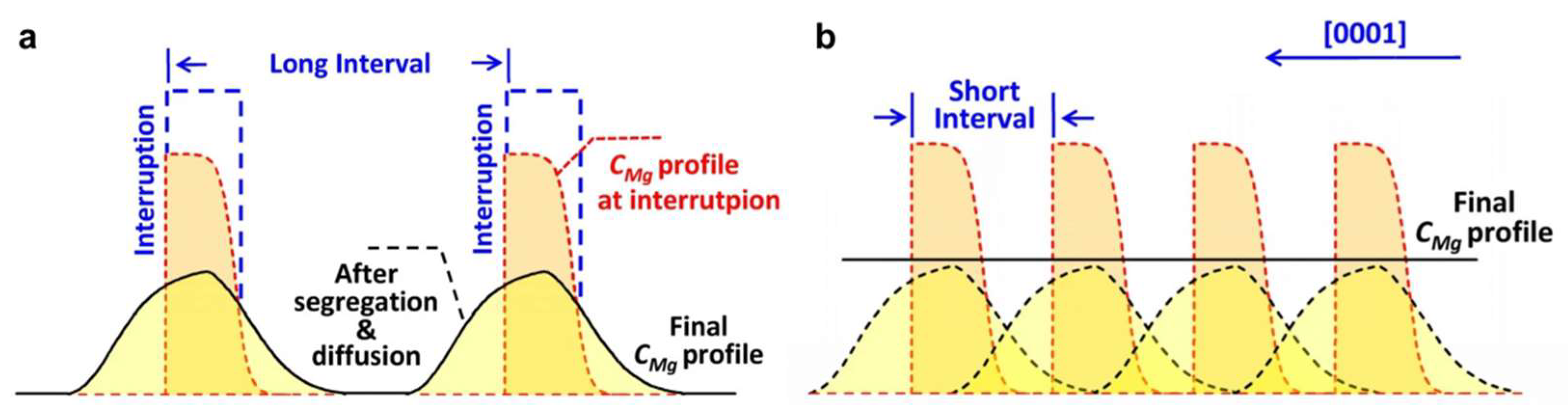
  106. Jiang, K.; Sun, X.; Shi, Z.; Zang, H.; Ben, J.; Deng, H.X.; Li, D. Quantum engineering of non-equilibrium efficient p-doping in ultra-wide band-gap nitrides. Light Sci. Appl. 2021, 10, 69. [Google Scholar] [CrossRef]
  107. Bryan, Z.; Hoffmann, M.; Tweedie, J.; Kirste, R.; Callsen, G.; Bryan, I.; Rice, A.; Bobea, M.; Mita, S.; Xie, J.; et al. Fermi Level Control of Point Defects During Growth of Mg-Doped GaN. J. Electron. Mater. 2012, 42, 815–819. [Google Scholar] [CrossRef]
  108. Schubert, E.F.; Grieshaber, W.; Goepfert, I.D. Enhancement of deep acceptor activation in semiconductors by superlattice doping. Appl. Phys. Lett. 1996, 69, 3737–3739. [Google Scholar] [CrossRef] [Green Version]
  109. Tersoff, J. Enhanced Solubility of Impurities and Enhanced Diffusion near Crystal Surfaces. Phys. Rev. Lett. 1995, 74, 5080–5083. [Google Scholar] [CrossRef]
  110. Klump, A.; Hoffmann, M.P.; Kaess, F.; Tweedie, J.; Reddy, P.; Kirste, R.; Sitar, Z.; Collazo, R. Control of passivation and compensation in Mg-doped GaN by defect quasi Fermi level control. J. Appl. Phys. 2020, 127, 045702. [Google Scholar] [CrossRef]
  111. Wu, R.; Shen, L.; Yang, M.; Sha, Z.; Cai, Y.; Feng, Y.; Huang, Z.; Wu, Q. Enhancing hole concentration in AlN by Mg:O codoping: Ab initio study. Phys. Rev. B 2008, 77, 073203. [Google Scholar] [CrossRef]
  112. Aoyagi, Y.; Takeuchi, M.; Iwai, S.; Hirayama, H. High hole carrier concentration realized by alternative co-doping technique in metal organic chemical vapor deposition. Appl. Phys. Lett. 2011, 99, 112110. [Google Scholar] [CrossRef]
  113. Aoyagi, Y.; Takeuchi, M.; Iwai, S.; Hirayama, H. Formation of AlGaN and GaN epitaxial layer with high p-carrier concentration by pulse supply of source gases. AIP Adv. 2012, 2, 012177. [Google Scholar] [CrossRef]
  114. Al tahtamouni, T.M.; Lin, J.Y.; Jiang, H.X. Effects of Mg-doped AlN/AlGaN superlattices on properties of p-GaN contact layer and performance of deep ultraviolet light emitting diodes. AIP Adv. 2014, 4, 047122. [Google Scholar] [CrossRef]
  115. Nakarmi, M.L.; Kim, K.H.; Li, J.; Lin, J.Y.; Jiang, H.X. Enhanced p-type conduction in GaN and AlGaN by Mg--doping. Appl. Phys. Lett. 2003, 82, 3041–3043. [Google Scholar] [CrossRef]
  116. Chen, Y.; Wu, H.; Han, E.; Yue, G.; Chen, Z.; Wu, Z.; Wang, G.; Jiang, H. High hole concentration in p-type AlGaN by indium-surfactant-assisted Mg-delta doping. Appl. Phys. Lett. 2015, 106, 162102. [Google Scholar] [CrossRef]
  117. Kim, K.; Li, J.; Jin, S.; Lin, J.Y.; Jiang, H. III-nitride ultraviolet light-emitting diodes with delta doping. Appl. Phys. Lett. 2003, 83, 566–568. [Google Scholar] [CrossRef]
  118. Bayram, C.; Pau, J.; McClintock, R.; Razeghi, M. Performance enhancement of GaN ultraviolet avalanche photodiodes with p-type -doping. Appl. Phys. Lett. 2008, 92, 241103. [Google Scholar] [CrossRef]
  119. Li, T.; Simbrunner, C.; Wegscheider, M.; Navarro-Quezada, A.; Quast, M.; Schmidegg, K.; Bonanni, A. GaN:-Mg grown by MOVPE: Structural properties and their effect on the electronic and optical behavior. J. Cryst. Growth 2008, 310, 13–21. [Google Scholar] [CrossRef] [Green Version]
  120. Ambacher, O.; Smart, J.; Shealy, J.R.; Weimann, N.G.; Chu, K.; Murphy, M.; Schaff, W.J.; Eastman, L.F.; Dimitrov, R.; Wittmer, L.; et al. Two-dimensional electron gases induced by spontaneous and piezoelectric polarization charges in N- and Ga-face AlGaN/GaN heterostructures. J. Appl. Phys. 1999, 85, 3222–3233. [Google Scholar] [CrossRef] [Green Version]
  121. Li, S.; Ware, M.; Wu, J.; Minor, P.; Wang, Z.; Wu, Z.; Jiang, Y.; Salamo, G.J. Polarization induced pn-junction without dopant in graded AlGaN coherently strained on GaN. Appl. Phys. Lett. 2012, 101, 122103. [Google Scholar] [CrossRef]
  122. Simon, J.; Protasenko, V.; Lian, C.; Xing, H.; Jena, D. Polarization-Induced Hole Doping in Wide–Band-Gap Uniaxial Semiconductor Heterostructures. Science 2010, 327, 60–64. [Google Scholar] [CrossRef] [Green Version]
  123. Xi, Y.; Chen, K.; Mont, F.; Kim, J.K.; Schubert, E.; Liu, W.; Li, X.; Smart, J. Comparative study of n-type AlGaN grown on sapphire by using a superlattice layer and a low-temperature AlN interlayer. J. Cryst. Growth 2007, 299, 59–62. [Google Scholar] [CrossRef]
  124. Kozodoy, P.; Hansen, M.; DenBaars, S.P.; Mishra, U.K. Enhanced Mg doping efficiency in Al0.2Ga0.8N/GaN superlattices. Appl. Phys. Lett. 1999, 74, 3681–3683. [Google Scholar] [CrossRef]
  125. Kumakura, K.; Makimoto, T.; Kobayashi, N. Enhanced Hole Generation in Mg-Doped AlGaN/GaN Superlattices Due to Piezoelectric Field. Jpn. J. Appl. Phys. 2000, 39, 2428–2430. [Google Scholar] [CrossRef]
  126. Zhang, J.; Gao, Y.; Zhou, L.; Gil, Y.U.; Kim, K.M. Surface hole gas enabled transparent deep ultraviolet light-emitting diode. Semicond. Sci. Technol. 2018, 33, 07LT01. [Google Scholar] [CrossRef]
  127. Zheng, T.; Lin, W.; Liu, R.; Cai, D.; Li, J.; Li, S.; Kang, J. Improved p-type conductivity in Al-rich AlGaN using multidimensional Mg-doped superlattices. Sci. Rep. 2016, 6, 21897. [Google Scholar] [CrossRef] [PubMed] [Green Version]
  128. Ebata, K.; Nishinaka, J.; Taniyasu, Y.; Kumakura, K. High hole concentration in Mg-doped AlN/AlGaN superlattices with high Al content. Jpn. J. Appl. Phys. 2018, 57, 04FH09. [Google Scholar] [CrossRef]
  129. Allerman, A.; Crawford, M.; Miller, M.; Lee, S.R. Growth and characterization of Mg-doped AlGaN–AlN short-period superlattices for deep-UV optoelectronic devices. J. Cryst. Growth 2010, 312, 756–761. [Google Scholar] [CrossRef]
  130. Wang, J.; Wang, M.; Xu, F.; Liu, B.; Lang, J.; Zhang, N.; Kang, X.; Qin, Z.; Yang, X.; Wang, X.Q.; et al. Sub-nanometer ultrathin epitaxy of AlGaN and its application in efficient doping. Light Sci. Appl. 2022, 11, 71. [Google Scholar] [CrossRef]
  131. Nam, K.B.; Li, J.; Nakarmi, M.L.; Lin, J.Y.; Jiang, H.X. Unique optical properties of AlGaN alloys and related ultraviolet emitters. Appl. Phys. Lett. 2004, 84, 5264–5266. [Google Scholar] [CrossRef] [Green Version]
  132. Kolbe, T.; Knauer, A.; Chua, C.; Yang, Z.; Einfeldt, S.; Vogt, P.; Johnson, N.M.; Weyers, M.; Kneissl, M. Optical polarization characteristics of ultraviolet (In)(Al)GaN multiple quantum well light emitting diodes. Appl. Phys. Lett. 2010, 97, 171105. [Google Scholar] [CrossRef]
  133. Ryu, H.Y.; Choi, I.G.; Choi, H.S.; Shim, J.I. Investigation of Light Extraction Efficiency in AlGaN Deep-Ultraviolet Light-Emitting Diodes. Appl. Phys. Express 2013, 6, 062101. [Google Scholar] [CrossRef]
  134. Muhin, A.; Guttmann, M.; Kuhn, C.; Mickein, E.; Aparici, J.R.; Ziffer, E.; Susilo, N.; Sulmoni, L.; Wernicke, T.; Kneissl, M. Vertical conductivity and Poole–Frenkel-ionization of Mg acceptorsin AlGaN short-period superlattices with high Al mole fraction. Appl. Phys. Lett. 2020, 117, 252101. [Google Scholar] [CrossRef]
  135. Guttmann, M.; Susilo, A.; Sulmoni, L.; Susilo, N.; Ziffer, E.; Wernicke, T.; Kneissl, M. Light extraction efficiency and internal quantum efficiency of fully UVC-transparent AlGaN based LEDs. J. Phys. D: Appl. Phys. 2021, 54, 335101. [Google Scholar] [CrossRef]
  136. Khan, M.A.; Maeda, N.; Jo, M.; Akamatsu, Y.; Tanabe, R.; Yamada, Y.; Hirayama, H. 13 mW operation of a 295–310 nm AlGaN UV-B LED with a p-AlGaN transparent contact layer for real world applications. J. Mater. Chem. C 2018, 7, 143–152. [Google Scholar] [CrossRef] [Green Version]
  137. Nakashima, T.; Takeda, K.; Shinzato, H.; Iwaya, M.; Kamiyama, S.; Takeuchi, T.; Akasaki, I.; Amano, H. Combination of Indium–Tin Oxide and SiO2/AlN Dielectric Multilayer Reflective Electrodes for Ultraviolet-Light-Emitting Diodes. Jpn. J. Appl. Phys. 2013, 52, 08JG07. [Google Scholar] [CrossRef]
  138. Kashima, Y.; Maeda, N.; Matsuura, E.; Jo, M.; Iwai, T.; Morita, T.; Kokubo, M.; Tashiro, T.; Kamimura, R.; Osada, Y.; et al. High external quantum efficiency (10%) AlGaN-based deep-ultraviolet light-emitting diodes achieved by using highly reflective photonic crystal on p-AlGaN contact layer. Appl. Phys. Express 2017, 11, 012101. [Google Scholar] [CrossRef]
  139. Matsukura, Y.; Inazu, T.; Pernot, C.; Shibata, N.; Kushimoto, M.; Deki, M.; Honda, Y.; Amano, H. Improving light output power of AlGaN-based deep-ultraviolet light-emitting diodes by optimizing the optical thickness of p-layers. Appl. Phys. Express 2021, 14, 084004. [Google Scholar] [CrossRef]
  140. Schubert, M.F. Interband tunnel junctions for wurtzite III-nitride semiconductors based on heterointerface polarization charges. Phys. Rev. B 2010, 81, 035303. [Google Scholar] [CrossRef]
  141. Mehnke, F.; Kuhn, C.; Guttmann, M.; Sulmoni, L.; Montag, V.; Glaab, J.; Wernicke, T.; Kneissl, M. Electrical and optical characteristics of highly transparent MOVPE-grown AlGaN-based tunnel heterojunction LEDs emitting at 232 nm. Photon. Res. 2021, 9, 1117–1123. [Google Scholar] [CrossRef]
  142. Banal, R.G.; Funato, M.; Kawakami, Y. Optical anisotropy in [0001]-oriented AlxGa1−xN/AlN quantum wells (x > 0.69). Phys. Rev. B 2009, 79, 121308. [Google Scholar] [CrossRef] [Green Version]
  143. Reich, C.; Guttmann, M.; Feneberg, M.; Wernicke, T.; Mehnke, F.; Kuhn, C.; Rass, J.; Lapeyrade, M.; Einfeldt, S.; Knauer, A.; et al. Strongly transverse-electric-polarized emission from deep ultraviolet AlGaN quantum well light emitting diodes. Appl. Phys. Lett. 2015, 107, 142101. [Google Scholar] [CrossRef]
  144. Zheng, J.; Li, J.; Zhong, Z.; Lin, W.; Chen, L.; Li, K.; Wang, X.; Chou, C.; Li, S.; Kang, J. Effect of electrical injection-induced stress on interband transitions in high Al content AlGaN MQWs. RSC Adv. 2017, 7, 55157–55162. [Google Scholar] [CrossRef]
  145. Bryan, Z.; Bryan, I.; Mita, S.; Tweedie, J.; Sitar, Z.; Collazo, R. Strain dependence on polarization properties of AlGaN and AlGaN-based ultraviolet lasers grown on AlN substrates. Appl. Phys. Lett. 2015, 106, 232101. [Google Scholar] [CrossRef]
  146. Long, H.; Wang, S.; Dai, J.; Wu, F.; Zhang, J.; Chen, J.; Liang, R.; Feng, Z.; Chen, C. Internal strain induced significant enhancement of deep ultraviolet light extraction efficiency for AlGaN multiple quantum wells grown by MOCVD. Opt. Express 2018, 26, 680. [Google Scholar] [CrossRef]
  147. Zhang, S.; Zhang, Y.; Tang, N.; Wang, W.; Chen, X.; Fu, L.; He, C.; Lv, Y.; Feng, Z.; Xu, F.; et al. Compressive strain induced enhancement of transverse-electric polarized ultraviolet light emission for AlGaN quantum wells. Superlattices Microstruct. 2020, 150, 106749. [Google Scholar] [CrossRef]
  148. Bayerl, D.; Islam, S.; Jones, C.M.; Protasenko, V.; Jena, D.; Kioupakis, E. Deep ultraviolet emission from ultra-thin GaN/AlN heterostructures. Appl. Phys. Lett. 2016, 109, 241102. [Google Scholar] [CrossRef]
  149. Gao, N.; Chen, J.; Feng, X.; Lu, S.; Lin, W.; Li, J.; Chen, H.; Huang, K.; Kang, J. Strain engineering of digitally alloyed AlN/GaN nanorods for far-UVC emission as short as 220 nm. Opt. Mater. Express 2021, 11, 1282. [Google Scholar] [CrossRef]
Figure 1. Partial applications of AlGaN-based LEDs of (a) UV band and (b) below 250 nm. Images are partially from internet. (c) Schematic of sterilization on the skin by high UVC below 250 nm.
Crystals 12 01812 g001
Figure 2. Summary of the reported (a) EQE, (b) LOP, and (c) WPE of 250 nm and sub-250 nm LEDs in dependence of emission wavelength in recent literature [11,16,17,18,19,20,21,22,26,35,36,37].
Crystals 12 01812 g002
Figure 3. Schematic diagram for (a) epitaxial structure and (b) energy band structure of a typical AlGaN-based UV LED, which are suitable for sub-250 nm LEDs, too.
Crystals 12 01812 g003
Figure 4. (a) Measured on-wafer EQE, simulated on-wafer LEE and corresponding product of RRE and CIE as a function of the emission wavelength [10]. (b) IQE as the function of DD at a weak excitation with the carrier density of 1 × 1018 cm−3 [39].
Crystals 12 01812 g004
Figure 6. (a) Current density dependent EQE under CW bias. Sample A includes an EBL graded from an Al composition of ~95% to ~75%. Sample C is identical to Sample A, except that its EBL is a uniform Al0.75Ga0.25N:Mg layer with the same thickness [36]. (b) The EQE of DUV LEDs with different wavelength with an MQB and a single barrier EBL [85].
Crystals 12 01812 g006
Figure 7. Conduction band diagrams of the active region of the DUV LED (a) without (LED A) and with (LED B) inserting thin layers in the QBs [90], (b) without (structure A) and with (structure B) asymmetrical concave QBs [91], (c) without (upper) and with (lower) delta-accelerating QBs [92], (d) without strip-in-a-barrier structure but EBL (LED 1), with strip-in-a-barrier structure and EBL (LED 2), with strip-in-a-barrier structure but EBL (LED 3) [93], (e) constant Al content (Device A) and gradually increasing Al content (Device B) LQB, [94] and (f) constant Al content (Device A) and gradually decreasing Al content (Device B and C) LQB [95].
Crystals 12 01812 g007
Figure 9. Schematic diagram of the Mg incorporation behavior in the AlGaN grown by the MSE technique. (a) When the interruption interval is long, only some peaks distribute locally at the interruptions after Mg segregation and diffusion. (b) After optimizing the interruption interval, a high and uniform Mg distribution over the entire AlGaN epilayer was achieved [100].
Crystals 12 01812 g009
Figure 10. The VBM modulation mode to lower the acceptor Ea. Acceptors are randomly doped in (a) AlN and (c) GaN. Both have high Ea in this condition. (b) GaN QDs are embedded in the AlN matrix and acceptors are doped in the AlN matrix and concentrate near the interface [106].
Crystals 12 01812 g010
Figure 11. Schematic structure of (a) the LEDs with and without a PhC on the p-AlGaN contact layer [138] and (b) the flip-chip LED with two light paths [139]. (c) Schematic diagram of homogeneous tunnel junction structure and its corresponding energy band as well as carrier transport.
Crystals 12 01812 g011
Figure 12. (a) Schematic energy band structures for unstrained AlGaN, strained AlGaN on AlN, and AlGaN/AlN QW near the Γ point with high Al content. CB denotes the conduction band. (b) Emission polarization mode as function of Al composition and well width [142]. (c) DOP of the emission from an AlGaN-based QW with 1.5 nm thickness pseudomorphically grown on AlN bulk calculated by k·p theory [143].
Crystals 12 01812 g012
Publisher’s Note: MDPI stays neutral with regard to jurisdictional claims in published maps and institutional affiliations.

