Article

Effect of Process Parameters on the Microstructure of Aluminum Alloys Made via Ultrasonic Additive Manufacturing

by
Gowtham Venkatraman
,
Leon M. Headings
and
Marcelo J. Dapino
*
NSF IUCRC Smart Vehicle Concepts Center, Department of Mechanical and Aerospace Engineering, The Ohio State University, 201 W 19th Ave., Columbus, OH 43210, USA
*
Author to whom correspondence should be addressed.
Crystals 2022, 12(12), 1696; https://doi.org/10.3390/cryst12121696
Submission received: 1 November 2022 / Revised: 14 November 2022 / Accepted: 16 November 2022 / Published: 23 November 2022

Abstract

:
Ultrasonic additive manufacturing (UAM) has garnered significant interest in the aerospace and automotive industries for its structural lightweighting and multi-material joining capabilities. This paper details the investigation on the effect of process variables on the resultant microstructure of the built-up part using UAM for aluminum 6061. The degree of recrystallization is quantified, and an energy metric, defined using the Read–Shockley relationship, is used to build an energy map of the welded part. The total energy stored in the resultant weld interface microstructure is quantified as a fraction of the input and is found to be about 0.1%. The width, average grain size, and percentage of High Angle Grain Boundaries (% HAGB) were used to compare microstructures of builds prepared using different processing conditions. Welding subsequent weld layers was not found to affect the previous welded layers. The effect of vibration amplitude and travel speed on the as-built microstructure were investigated, and the width of the interface was found to more than double when the weld amplitude is increased from the threshold value for joining (23 μm) and then stabilize at higher weld amplitudes. A better understanding of the effect of processing parameters on as-welded microstructures will assist parameter selection for UAM.

1. Introduction

Ultrasonic additive manufacturing (UAM) is an additive manufacturing technology which combines solid-state ultrasonic metal welding, CNC machining, and mechanized foil layering to create large gapless near net-shape metallic parts. Its integration with subtractive processes enables the fabrication of complex internal features, embedment of objects, and net shaping of parts, as detailed in [1,2]. The low formation temperature of the UAM process also allows the integration of temperature-sensitive components, smart materials, cooling channels, organic polymers, and electronics into metal matrices.
The microstructure of structures built by UAM has been extensively investigated using electron backscatter diffraction (EBSD). Such investigations in UAM of aluminum alloys [3,4,5,6] have shown that the weld interface comprises of small, mostly equiaxed recrystallized grains. Recrystallization was observed to only occur at very local interface regions due to local shear deformation, while the bulk region of each layer still remains mostly unaffected. In [7], the extensive grain refinement at the metal–metal interfacial bonds was attributed to the continuous dynamic recrystallization process which is driven by the high strain rate plastic deformation and associated adiabatic heating at temperatures below 50% of the melting point of the constituent metals. A comprehensive review of microstructure evolution in UAM can be found in [8].
The lower formation temperature is expected to suppress the formation of brittle intermetallics, enabling the joining of different metal combinations using UAM [9]. Other work in [10] showed that some metal interdiffusion could be observed between metallized optical fibers and a different parent metal such as Al–Cu or Ni–Au. Using thermocouples embedded at the weld interface, the work in [11] showed that the formation temperature reaches a peak value near 150 °C for welding aluminum and copper alloys with a 9 kW welder. Other work in [12] measured a temperature increase between 400 and 700 K for the welding of 4130 carbon steel, which needs higher ultrasonic power for successful bonding.
There has also been work on quantifying the amount of grain growth that occurs during the ultrasonic welding of nano-crystalline materials as a function of weld pressure and weld time [13]. Ion-channeling contrast imaging using a focused ion beam (FIB) has also been conducted for Al 3003-H18 to discover thin bands of nanograins near the welder and the modification in the grain morphology is explained by the accumulative thermomechanical processes due to sequential bonding of foils [14]. Some studies such as [15] qualitatively analyzed SEM (scanning electron microscope) scans of UAM-ed Al 1100-O samples fabricated using different process parameters but neither a quantitative analysis to compare the samples nor any quantification of stored energy was conducted.
Two key metrics obtained from the EBSD analysis are the mean grain diameter and fraction of high angle (>15 degrees) grain boundaries [16]. The raw EBSD data can be re-analyzed to yield a substantial amount of quantitative information about grains, subgrains, and grain boundaries [17]. Open-source toolboxes such as MTEX in MATLAB provide versatile functions to import, analyze, and visualize diffraction EBSD data to estimate an orientation density function, to compute texture characteristics, to model orientation density functions, to simulate pole figure or EBSD data, and to manipulate pixel-level EBSD data directly [18].
The energy stored in the microstructure can be quantified from EBSD scans using the Read–Shockley equation, as shown for the accumulative roll bonding (ARB) process in [19]. The thermodynamic aspects of the conversion of cold working due to plastic deformation into stored energy in the microstructure is detailed in [20]. The stored energy in manufacturing processes such as rolling can be characterized using SEM and TEM (transmission electron microscopy) [21]. This work expands the techniques developed in these studies to understand the flow of energy from the input electrical energy at the transducers to the grain boundaries in the resulting welded structure for the UAM process.
Work on other additive manufacturing (AM) technologies on the effect of process parameters on the texture using SEM has been conducted in [22] for laser-based metal AM on Inconel. Such work can be important to understand how changing process parameters influences different aspects of the microstructure and guide the selection of process parameters to maximize bond strength, shown in work in [23] for laser powder-bed AM of stainless steel. In this work, EBSD and SEM techniques are used to understand the effect of UAM process parameters on the dynamic recrystallization process during bond formation. Nanoindentation is used to verify the size of the weld interface region with recrystallized grains. The energy stored in the weld interface microstructure is also quantified to compare to the input energy of the process. To this end, two studies are conducted for the UAM of 6061 aluminum, which is a commonly used alloy of aluminum in the aerospace and automotive industries. The first study investigates the effect of subsequent weld layers on the microstructures of the previously welded UAM weld interface, up to nine additional layers. The second study investigates the effect of two key process parameters, weld amplitude and weld speed, on the weld interface microstructure to better understand the flow of energy in the process from the electrical input to the microstructure.

2. Materials and Methods

2.1. Materials

All the studies were conducted using Al 6061-H18 alloy as the feedstock material. The composition of the alloy can be obtained from [24]. The thickness of the 25.4 mm (1 inch) wide foil feedstock is 152 μm. The samples were welded using a 9 kW UAM welder onto an Al 6061-T6 baseplate, and the nominal UAM process conditions used were: 32 μm weld amplitude, 5000 N weld force, and 84.67 mm/s (200 in/min) weld speed. In Section 3.2, the weld amplitude and weld speed were varied to study the effect of process parameters on the weld interface microstructure.

2.2. Electron Backscatter Diffraction (EBSD)

EBSD is performed in a SEM, utilizing the tool to create an array of diffraction patterns that are captured on a detector. A diffraction pattern is captured at every point in the SEM scan, which are then indexed and the crystal orientation at each point is determined. For EBSD, a very carefully polished sample is required, which is obtained by polishing sections of UAM samples using 0.05 μm colloidal silica solution. EBSD is an excellent tool for measuring crystal orientations and symmetry. The measurements are limited by the EBSD resolution of 0.25 μm, and hence smaller grains cannot be resolved using the detector. This will lead to an underestimation of the stored energy due to the smoothing algorithm used.

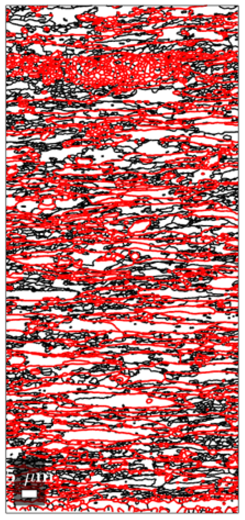
2.3. Quantitative EBSD Analysis

For data cleanup and processing, the MTEX toolbox by Ralf Hielscher is used (https://mtex-toolbox.github.io/, accessed on 27 September 2018). The MTEX toolbox within MATLAB is used to process the raw data to obtain quantitative metrics: grain size distribution, misorientation angle distribution, and stored energy. It is also used to denoise and smooth the data to plot inverse pole figure (IPF) maps and grain boundary maps. Single mis-indexed pixels are deleted and reconstructed together with single nonindexed pixels. The raw scan data from the EBSD detector has many regions with low confidence due to systematic noise, and hence contains many points that are not indexed (about 0.4%) or with low (<5%) confidence index (17%). Non-indexed areas less than two pixels wide are filled during noise removal using a half-quadratic filter. The alpha coefficient for the filter was chosen to by 0.25 and the level was chosen to be 3. A subgrain detection algorithm is used to identify the grain boundaries. A minimum subgrain size of 3 pixels and a boundary misorientation threshold of two degrees were used. A grain boundary is identified as a high-angle grain boundary (HAGB) if the misorientation between the neighboring pixels exceeds 15 degrees. Figure 1 shows these HAGBs in red and the other boundaries in black. The interface region is observed to have a high concentration of HAGBs.
Figure 2 illustrates a visualization of the microstructure of the UAM weld interface in Al 6061-H18 where the different colors denote the different orientations of each pixel. The SEM imaging data was provided by collaborators at Battelle Memorial Institute. The weld interface is approximately 15 μm tall. The bulk region of the foils away from the interface retains its pre-weld elongated microstructure typical of as-received rolled foil. For the weld interface in the sample shown in Figure 2, the mean grain diameter is 0.72 μm and the fraction of high angle grain boundaries is 0.66. There have been attempts at modeling the grain diameter d post-UAM using the Zener–Hollomon parameter Z h which found that the subgrain size is related to the strain rate ε ˙ and the peak temperature T p as follows [25]:
d = ( 0.6 + 0.08 log Z h ) 1 ,
Z h = ε ˙ exp 18772 T p .
Using typical values for strain rate (10,000/s) and peak temperature (373 K) for the UAM of Al 6061-H18, the subgrain size estimated is 0.24 μm. This mismatch is attributed to the limited 0.25 μm resolution of the EBSD detector used and the minimum pixel size of 3 per subgrain, and the background noise in the backscatter image near the weld interface is attributed to the severe deformation.

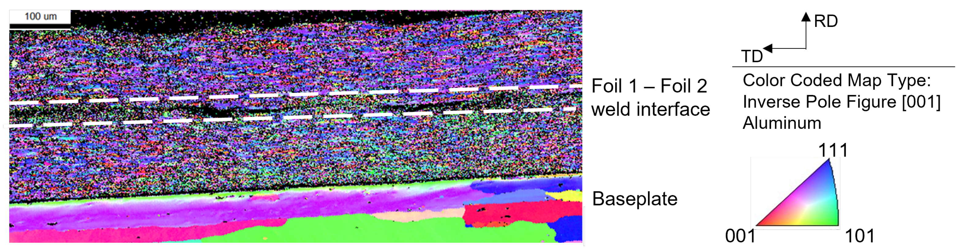
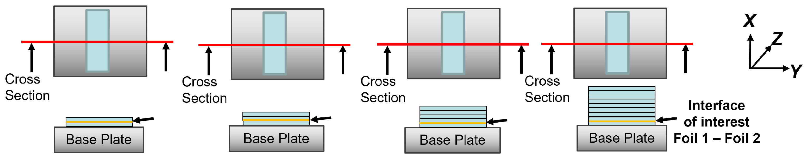
2.4. Weld Interface Identification

The location of the weld interface needs to be determined quantitatively from the raw EBSD data. The fraction of indexed points was found to be a reliable metric to determine this location since the interface has severely deformed material with small recrystallized grains, some of which are smaller than the 0.25 μm resolution of the detector and, thus, unable to be accurately indexed. To this end, a 2 μm window is spanned across the sample to identify the interface center. The corresponding fraction of indexed points is shown in Figure 3. The width of the interface was identified by iterating over increasing widths from the center point until an inflection point was obtained in the mean grain size within the region.

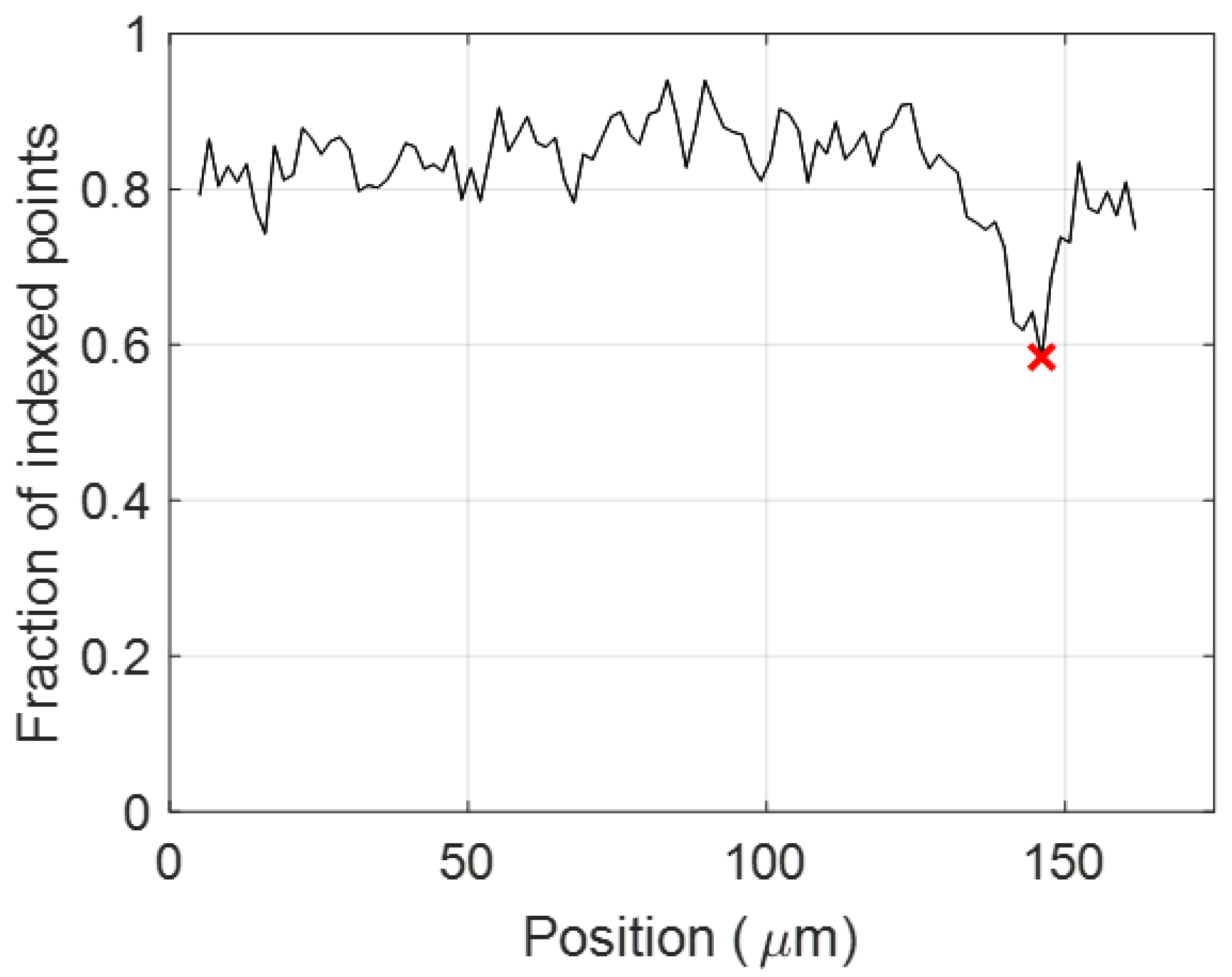
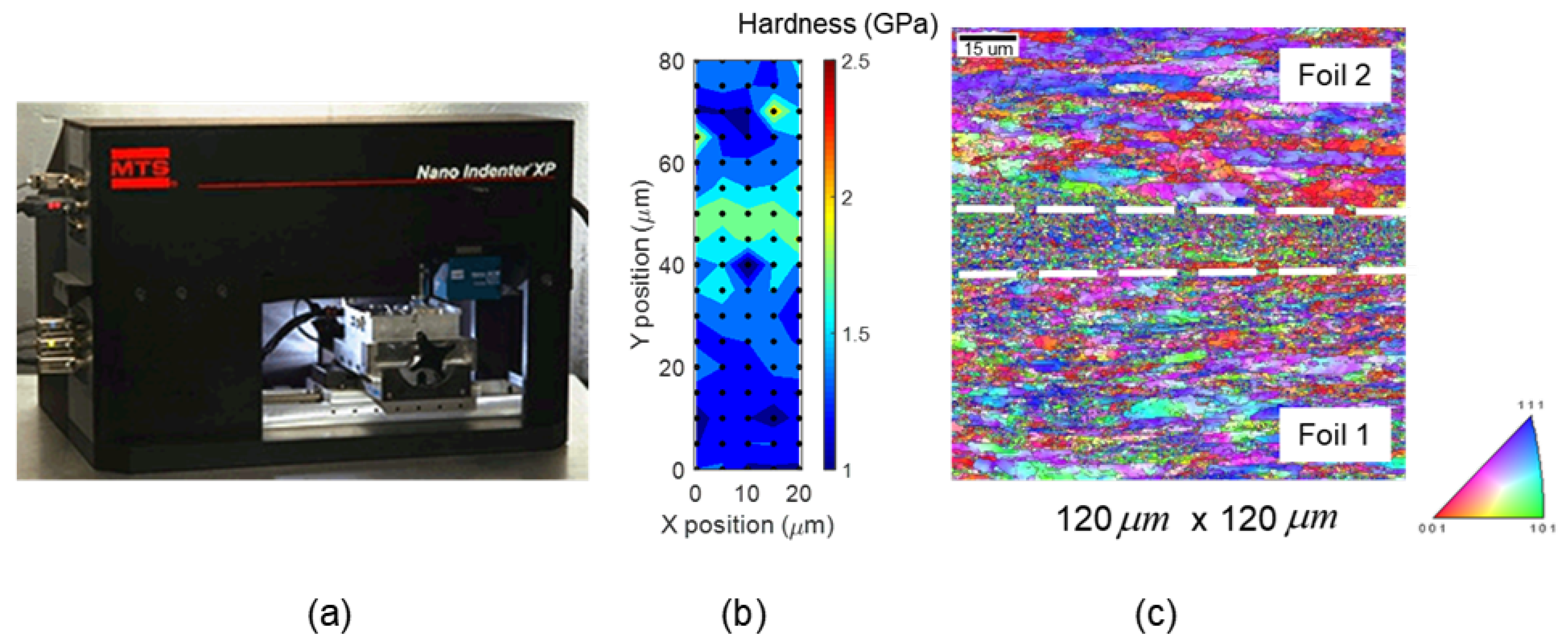
2.5. Nanoindentation for Interface Identification

Nanoindentation was used to verify the width of the region with recrystallized grains as measured using EBSD in Section 2.2. The technique measured the local hardness value of the Al matrix near the foil 1–foil 2 weld interface. The samples were prepared by welding two layers of Al 6061-H18 on an Al 6061-T6 baseplate. Previous work on hardness mapping of Al 3003-O/SiC composite matrices fabricated using UAM discovered that the hardness increase near the interfaces of welds matched with the expected increase due to refined grains using the Hall–Petch relationship [26]. Nanoindentation has also been used as an alternative to microscopy to identify intermetallic compounds in laser joining processes from local hardness increases [27]. The method has applications beyond measuring hardness, and can be used to measure the local yield strength and Young’s modulus [28]. It was found in [29] that yield stress measurements by indentation and micro-traction experiments are comparable for electric arc welds of Al 6061-T6.
The minimum spacing between indents is determined by the polishing particle diameter (0.05 μm), and was computed to be 3 μm. Another factor to consider is ISE or indent size effect which is a hardness-depth relationship observed for most materials that exhibit artificially higher hardness measurements at low penetration depths of the indenter into the material. This dependence can be very different for different alloys of steel, brass, and aluminum [30], and hence a study needs to be conducted to determine the appropriate indent size. This effect can be more pronounced in softer materials like aluminum [31]. To this end, an array of indentations were created on an Al 6061-T6 baseplate using loads ranging from 0.4 gf to 50 gf. The hardness of the baseplate was found to plateau for an indentation depth of 2 μm, and hence a 0.4 gf load was chosen which results in an indent spacing resolution of 5 μm.
The resulting hardness map is shown in Figure 4b, where the Al 6061-T6 baseplate in the bottom has the highest hardness values, and a clear 10–15 μm-wide interface region is observed between the two Al 6061-H18 weld foils with higher hardness when compared to the surrounding bulk material. The size of the weld interface region matches the weld interface width estimate from EBSD analysis (14 μm) shown in Figure 2.
The weld interface region was observed to have a measurably higher hardness than bulk foil, which is expected from the Hall–Petch relationship due to the small equiaxed grains. The bulk Al 6061-H18 material hardness is identical to the as-received foil hardness value since the H-18 temper has a large amount of cold work (upto 80%) cold-worked, and has limited margin to be further work-hardened by the thermo-mechanical processes in UAM. It is expected that the bulk hardness of annealed materials such as Al 6061-O will be higher after UAM.

3. Estimation of Energy Storage in the Microstructure

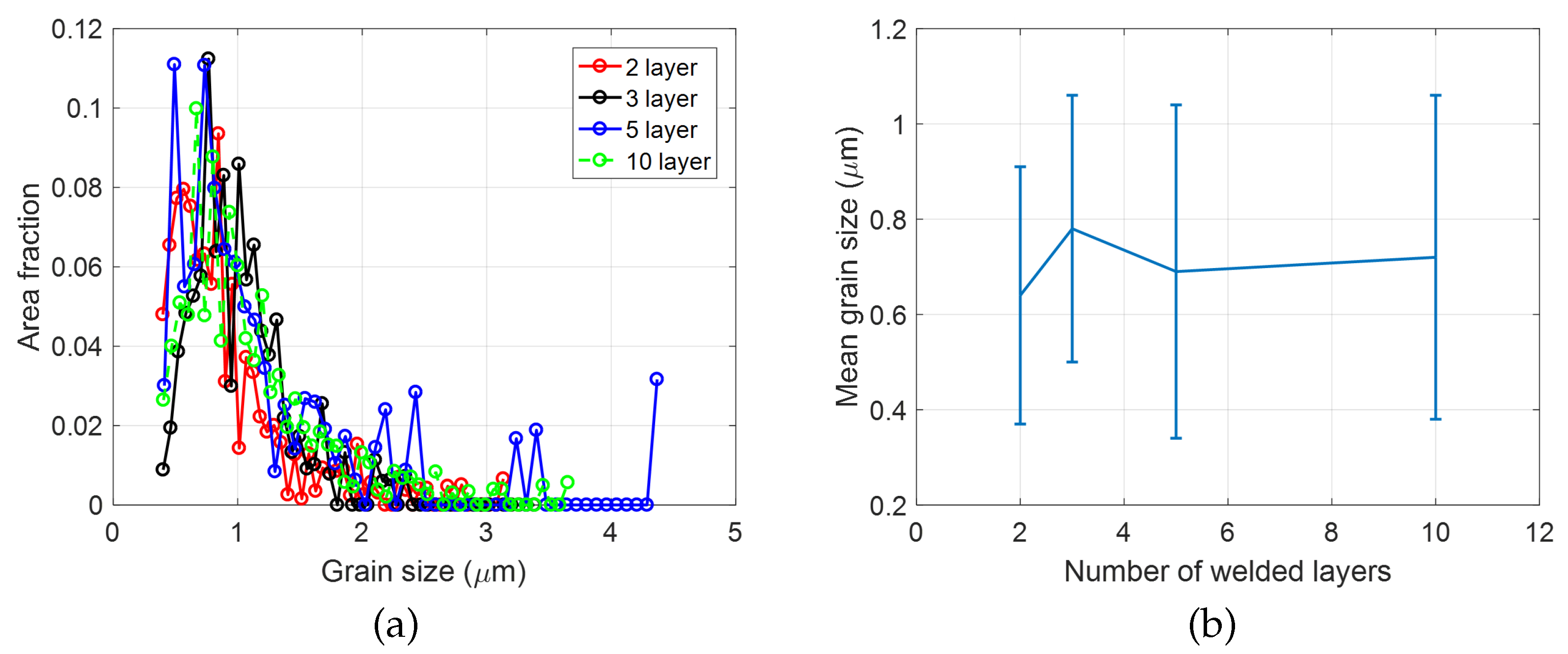
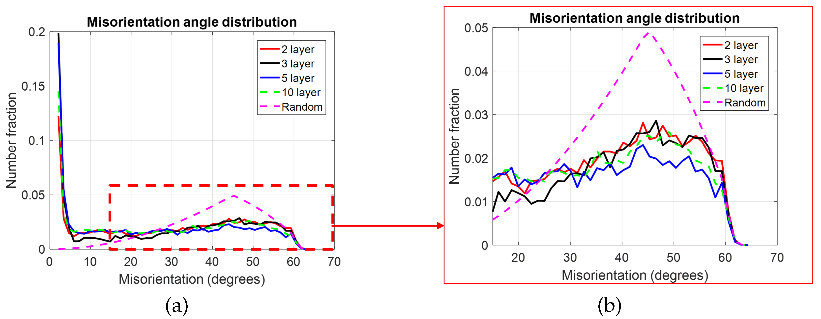
3.1. Study A: Effect of Subsequent Weld Layers

Al 6061-H18 samples with 2, 3, 5, and 10 layers were welded onto a 12.7 mm (0.5 inch) thick Al 6061-T6 baseplate using identical UAM process conditions: 32 μm weld amplitude, 5000 N weld force, and 84.67 mm/s (200 in/min) weld speed. The thickness of the 25.4 mm (1 inch) wide foil feedstock is 152 μm. The objective of the study is to investigate the effect of subsequent weld layers on the weld interface microstructure. The samples were sectioned as shown in Figure 5.
Figure 6 show cross-section images of the four samples taken using the optical microscope included in the Leco LM 100AT hardness tester. The Al 6061-T6 baseplate and the Al 6061-H18 foils can be distinguished by the difference in color due to the difference in precipitates (shown as black spots) in the aluminum matrix. Voids are not observed between the first and second foil in any of the samples. A large void is seen in the foil 9–foil 10 interface for the 10-layer sample in Figure 6d but that may be attributed to decreasing weld quality as build height increases for builds without power compensation [32].
EBSD analysis was conducted to quantify differences in the weld interface microstructure between the first and second foil welded due to subsequent layers being welded. The EBSD measurements used a detector with a point resolution of 0.25 μm. Inverse pole figures (IPF) are a visual representation of grain orientations and grain boundaries. The IPF plots in Figure 7 show a dense collection of refined grains at the foil–foil weld interface. Most grains away from the interface retain their as-rolled texture and are elongated along the direction of rolling, but some refined grains are found away from the weld interface.
Figure 8a shows that the histograms of grain sizes near the weld interface for the four samples are very similar, which indicates that the deformation due to subsequent welding does not induce further grain refinement in the foil 1—foil 2 interface. The mean grain size shown in Figure 8b is also similar for all the samples at around 0.7 μm. The heat generated may be expected to cause grain growth, as detailed in [14], but the histogram shows that this effect is also minimal for the process parameters and materials used.
Figure 9a compares the misorientation angle distribution with the theoretical Mckenzie distribution for equiaxed grains and it is found that the four samples have similar misorientation angle distributions. The zoomed image in Figure 9b shows that there is a greater fraction of grains exhibiting higher misorientations with their neighbors than what would be expected for rolled foil material, where no peak would be expected at high misorientations.
Grain refinement and misorientation are direct indicators of the degree of recrystallization, hence mean grain diameter and fraction of HAGBs in the weld interface region are used as a comparison metric in Table 1. Interface width shows a slight increase for the 5- and 10-layer samples, but given that the resolution of the EBSD detector is 0.25 μm, the interface width can be assumed to be constant at 14 μm. Average grain diameter does not significantly increase, and the differences between the cases are within error bounds. The proportion of high angle grain boundaries, a metric of recrystallization, is also within 10% variation from the value for the two-layer sample. Within the range of parameters tested, no significant difference in the microstructure was detected using mean grain diameter and fraction of HAGBs as metrics. Using these metrics, the effect of subsequent welds on the weld microstructure of Al 6061-H18 UAM builds is not significant up to 10 layers of build up.

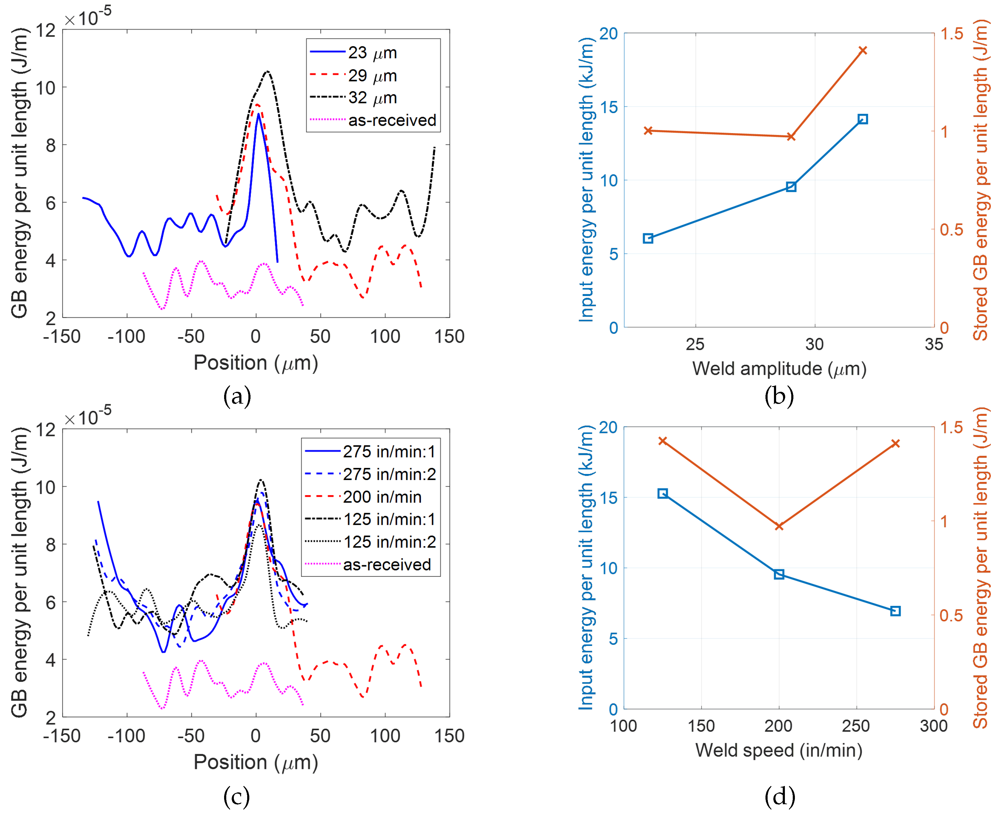
3.2. Study B: Effect of Process Settings

The objective of this study is to quantify the effect of UAM process parameters on the weld interface microstructure by measuring the energy stored in the microstructure. Trends between weld parameters used and the energy stored in the microstructure are obtained to guide mapping of the energy flow in the UAM process from the input electrical energy to the weld interface microstructure. To this end, Al 6061-H18 UAM samples with two layers were prepared and in situ process signals were measured for 10 different parameter sets, varying welder vibration amplitude and weld speed. Weld force was not varied based on previous work in [24] showing no statistical dependence of weld strength on weld force.
The weld force was thus fixed at a value of 5000 N. The lowest welder vibration amplitude at which stick occurs was found to be 21 μm. Hence, 23 μm was chosen as the lowest parameter value for amplitude of welder vibration. The upper limit of weld amplitude was chosen to avoid the sticking of the foil to the welder (nugget formation), which is observed at 35 μm. The nominal weld speed was chosen as 84.67 mm/s (200 in/min), and values were chosen on either side covering the operating parameter range of use, up to 179.92 mm/s (425 in/min). Weld speeds above 211.67 mm/s (500 in/min) are not typical.

3.2.1. Sample Fabrication

The length of each weld is 63.5 mm (2.5 inches). The weld foil is 0.152 μm thick, 25.4 mm (1 inch) wide Al 6061-H18. The Al 6061-T6 baseplate on which the foil was welded is 9 mm (0.35 inch) thick. Before welding, the baseplate was machined flat using a 25.4 mm (1 inch) diameter steel end-mill with a spindle speed of 5000 RPM at a feed rate of 63.5 mm/s (150 in/min). A single layer of foil was welded to the machined baseplate, and then a second layer was welded on top of the first layer. Both welds were made using the same weld parameters.
The first set of welds was processed by fixing the weld normal force at 5000 N, and the weld speed at 84.67 mm/s (200 in/min). The weld amplitude was varied between 23 μm and 35 μm, as shown in Figure 10a. A weld amplitude of 32 μm is the optimal value found for Al 6061-H18 foil on a 9 mm (0.35 inch) thick Al 6061-T6 baseplate [24]. The weld speed was varied by fixing the weld amplitude at 29 μm, as shown in Figure 10b. Transverse sections were cut such that the normal to the plane of cutting was along the rolling direction of the welder during fabrication. The sections were characterized using SEM and EBSD. A sample inverse pole figure is shown in Figure 2. The raw EBSD data was then analyzed using the MTEX toolbox in MATLAB.

3.2.2. In Situ Process Measurements

Weld power, weld speed, weld force, and voltage and current to the transducers are acquired using a National Instruments cDAQ-9178 for in situ process measurements. Two DAQ modules on an NI c-DAQ 9178 record the relevant signals. An NI 9222 module records signals sampled at 500 kHz and an NI 9239 module records signals sampled at 50 kHz, shown in Figure 11. All signals measured by a single DAQ module are synchronous. For this study only the NI 9239 signals were used. The different participating energies in UAM are discussed in the work of [33]. Input energy per unit length of the weld, E i p , is expressed as a function of the electrical power input and the traverse speed of the workpiece as
E i p = Electrical power input Weld speed .

3.2.3. Stored Energy Estimation

The energy stored in the microstructure S was computed using the Read–Shockley equation to be
S = θ Ω G B · γ G B · θ θ m ( 1 ln θ θ m ) , if θ θ m 1 , θ > θ m ,
where θ is the angle of misorientation between a boundary pixel and its neighboring pixels, γ G B is the grain boundary energy density of aluminum (=0.324 J/m2 [34]), and Ω G B is the cross-section area. The value for pure aluminum is used and the effects of alloying elements and precipitates are ignored. The expression for the area assumes spherical grains, which is appropriate for the equiaxed grains in the weld interface region. The procedure to obtain the stored energy in the microstructure is detailed in Figure 12.
The energy values per unit length (in J/m) plotted were calculated by adding the grain boundary (GB) energy throughout the thickness of the UAM sample, with a peak near the weld interface, and deducting the GB energy in the as-received material of the same thickness, which was flat (or homogeneous). That is, stored GB energy = (GB energy in the UAM material)—(GB energy in the as-received material). Grains at the interface with low scan quality were not indexed (noisy), and were smoothed by data analysis, which leads to underestimation of the stored energy.
The stored energy profile for the UAM sample prepared using 5000 N weld force, 84.67 mm/s (200 in/min) weld speed, and 23 μm weld amplitude is compared against the as-received control foil in Figure 13. A clear peak at the weld interface which is 10% above the mean energy is observed in the energy histogram in Figure 13c, unlike the flat stored energy profile of the control sample in Figure 13d.
The stored energy profile of the four sample sets analyzed, control vs. samples prepared using 23, 29, and 32-μm weld amplitudes, are compared in Figure 14a. The cumulative stored energy is shown in Figure 14b. The stored GB energy (approximately 1 J/m) is about 0.1% of the input electrical energy, or the energy budget (approximately 10,000 J/m). There is a clear increase in interface width with increase in weld amplitude, and the width increase from the 23-μm to the 29-μm sample is greater than a factor of 2. The increase in the width from 29-μm to 32-μm samples is found to be minimal, with the highest energy stored in the 32 μm sample. This is believed to be due to the increase in the recrystallized region from a narrow region at the weld interface to a much wider region after a threshold weld amplitude is reached. Since 32 μm corresponds to the optimum weld amplitude found to give the highest interface shear strength, there seems to be a correspondence between the growth in the interface width and the increase in weld strength.
The stored energy profile of the other set of four samples analyzed, control vs. samples prepared using 52.91, 84.67, and 116.41 mm/s (125, 200, and 275 in/min) weld speeds, are compared in Figure 14c. No clear trend between the total stored energy and weld speed is observed, indicating that the weld amplitude of 29 μm is sufficiently higher than the threshold parameters required, such that there is no increase in the volume of recrystallized grains or the extent of grains refinement in the weld interface.

4. Conclusions

EBSD was used as a tool for quantitative comparison of the microstructures of parts welded using UAM. First, the effect of subsequent weld layers on weld microstructure was investigated by welding up to nine subsequent layers of foil over a Al 6061-H18 foil–foil weld built using the following settings: 32 μm weld amplitude, 5000 N weld force, and 84.67 mm/s (200 in/min) weld speed. A technique was developed to determine the location and width of the interface region. The interface width was estimated to be about 14 μm for the 2-, 3-, 5-, and 10-layer samples, which is within previous literature estimates of the weld interface region. Nanoindentation was also introduced as a companion testing method to obtain the location and size of the weld interface region as a region of higher hardness compared to the bulk microstructure. The interface width from nanoindentation matches with the estimate from EBSD.
The following metrics were developed to quantify differences in weld interface microstructure: interface width, average grain size, and percentage of grain boundaries that are high angle boundaries (% HAGB). The weld interface region was found to have a mean grain diameter around 0.7 μm and a 65% fraction of high angle grain boundaries. Within the margin of error of EBSD due to its resolution limit, there is no significant effect of subsequent welds on the UAM weld interface microstructure for the sample heights and dimensions investigated with the metrics used.
Second, a study was developed to quantify the effect of UAM process parameters on the weld interface microstructure by measuring the energy stored in the microstructure. The Read–Shockley relationship was used to compute the stored energy in the grain boundaries obtained from the EBSD scans using the MTEX toolbox. A peak in the density and magnitude of stored energy greater than 10% of the mean energy was observed at the weld interface, which was absent in the control as-received foil sample. The stored energy was found to be approximately 0.1% of the input energy at 1 J/m for the UAM samples. Stored energy and interface width were observed to monotonically increase with weld amplitude at a fixed weld speed of 84.67 mm/s (200 in/min), but found not to be sensitive to weld speed at a fixed weld amplitude of 29 μm. The study was conducted for aluminum 6061, but the techniques developed can be used for different tempers and alloy compositions for use in UAM. This work serves as a basis for future work to predict the mechanical properties of as-built parts using structure-property relationships built either empirically similar to the work of [35,36] or using virtual material testing similar to the work of [23].

Author Contributions

Conceptualization, G.V., L.M.H. and M.J.D.; methodology, G.V. and L.M.H.; software, G.V.; formal analysis, G.V. and L.M.H.; resources, M.J.D.; data curation, G.V.; writing—original draft preparation, G.V.; writing—review and editing, G.V., L.M.H. and M.J.D.; visualization, G.V.; supervision, M.J.D.; project administration, M.J.D.; funding acquisition, M.J.D. All authors have read and agreed to the published version of the manuscript.

Funding

Funding was provided by the member organizations of the Smart Vehicle Concepts Center (http://www.SmartVehicleCenter.org, accessed on 31 October 2022), a Phase III National Science Foundation Industry-University Cooperative Research Center under grant IIP 1738723. Any opinions, findings, and conclusions or recommendations expressed in this material are those of the authors and do not necessarily reflect the views of the National Science Foundation.

Institutional Review Board Statement

Not applicable.

Informed Consent Statement

Not applicable.

Data Availability Statement

Data sharing is not applicable to this article.

Acknowledgments

The authors would like to acknowledge the SEM measurements provided by the Battelle Memorial Institute, Columbus, Ohio by Melissa S. Roshon, Steven M. Risser, and Amy M. Heintz. The authors would also like to acknowledge the assistance of Antonio Ramirez and his lab for conducting the nanoindentation measurements.

Conflicts of Interest

The authors declare no conflict of interest. The funders had no role in the design of the study; in the collection, analyses, or interpretation of data; in the writing of the manuscript, or in the decision to publish the results.

References

  1. White, D. Ultrasonic consolidation of aluminum tooling. Adv. Mater. Process. 2003, 161, 64–65. [Google Scholar]
  2. Safavi, M.S.; Azarniya, A.; Farshbaf Ahmadipour, M.; Reddy, M.V. New-emerging approach for fabrication of near net shape aluminum matrix composites/nanocomposites: Ultrasonic additive manufacturing. J. Ultrafine Grained Nanostruct. Mater. 2019, 52, 188–196. [Google Scholar]
  3. Sridharan, N.; Wolcott, P.; Dapino, M.J.; Babu, S.S. Microstructure and texture evolution in aluminum and commercially pure titanium dissimilar welds fabricated using ultrasonic additive manufacturing. Scr. Mater. 2016, 117, 1–5. [Google Scholar] [CrossRef]
  4. Sriraman, M.R.; Babu, S.S.; Short, M. Bonding characteristics during very high power ultrasonic additive manufacturing of copper. Scr. Mater. 2010, 62, 560–563. [Google Scholar] [CrossRef]
  5. Shimizu, S.; Fujii, H.T.; Sato, Y.S.; Kokawa, H.; Sriraman, M.R.; Babu, S.S. Mechanism of weld formation during very-high-power ultrasonic additive manufacturing of Al alloy 6061. Acta Mater. 2014, 74, 234–243. [Google Scholar] [CrossRef]
  6. Li, P.; Wang, Z.; Diao, M.; Guo, C.; Wang, J.; Zhao, C.; Jiang, F. Dynamic recrystallization and recovery in very high-power ultrasonic additive manufacturing. Adv. Eng. Mater. 2021, 23, 2000958. [Google Scholar] [CrossRef]
  7. Sridharan, N.; Norfolk, M.; Babu, S.S. Characterization of steel-Ta dissimilar metal builds made using very high power ultrasonic additive manufacturing (VHP-UAM). Metall. Mater. Trans. 2016, 47, 2517–2528. [Google Scholar] [CrossRef]
  8. Li, D. A review of microstructure evolution during ultrasonic additive manufacturing. Int. J. Adv. Manuf. Technol. 2021, 113, 1–19. [Google Scholar] [CrossRef]
  9. Obielodan, J.O.; Ceylan, A.; Murr, L.E.; Stucker, B.E. Multi-material bonding in ultrasonic consolidation. Rapid Prototyp. J. 2010, 16, 180–188. [Google Scholar] [CrossRef]
  10. Pagan, M.; Petrie, C.; Leonard, D.; Sridharan, N.; Zinkle, S.; Babu, S.S. Interdiffusion of elements during ultrasonic additive manufacturing. Metall. Mater. Trans. A 2021, 52, 1142–1157. [Google Scholar] [CrossRef]
  11. Sriraman, M.R.; Gonser, M.; Fujii, H.T.; Babu, S.S.; Bloss, M. Thermal transients during processing of materials by very high power ultrasonic additive manufacturing. J. Mater. Process. Technol. 2011, 211, 1650–1657. [Google Scholar]
  12. Han, T. Ultrasonic Additive Manufacturing of Steel: Process, Modeling, and Characterization. Ph.D. Thesis, The Ohio State University, Columbus, OH, USA, 2020. [Google Scholar]
  13. Ward, A.A.; French, M.R.; Leonard, D.N.; Cordero, Z.C. Grain growth during ultrasonic welding of nanocrystalline alloys. J. Mater. Process. Technol. 2018, 254, 373–382. [Google Scholar]
  14. Fujii, H.T.; Sriraman, M.R.; Babu, S.S. Quantitative evaluation of bulk and interface microstructures in Al-3003 alloy builds made by very high power ultrasonic additive manufacturing. Metall. Mater. Trans. A 2011, 42, 4045–4055. [Google Scholar] [CrossRef]
  15. Li, P.; Wang, Z.; Diao, M.; Guo, C.; Wang, J.; Zhao, C.; Jiang, F. Effect of processing parameters on bond properties and microstructure evolution in ultrasonic additive manufacturing (UAM). Mater. Res. Express 2021, 8, 036507. [Google Scholar]
  16. Choi, S.; Jin, Y. Evaluation of stored energy in cold-rolled steels from EBSD data. Mater. Sci. Eng. A 2004, 371, 149–159. [Google Scholar]
  17. Humphreys, F.J. Reconstruction of grains and subgrains from electron backscatter diffraction maps. J. Microsc. 2004, 213, 247–256. [Google Scholar] [CrossRef] [PubMed]
  18. Bachmann, F.; Hielscher, R.; Schaeben, H. Texture analysis with MTEX–free and open source software toolbox. In Solid State Phenomena; Trans Tech Publications: Zurich, Switzerland, 2010; Volume 160, pp. 63–68. [Google Scholar]
  19. Kamikawa, N.; Huang, X.X.; Kondo, Y.; Furuhara, T.; Hansen, N. Stored energy and annealing behavior of heavily deformed aluminium. In Materials Science Forum; Trans Tech Publications: Zurich, Switzerland, 2012; Volume 715, pp. 367–372. [Google Scholar]
  20. Bever, M.B.; Holt, D.L.; Titchener, A.L. The stored energy of cold work. Prog. Mater. Sci. 1973, 17, 5–177. [Google Scholar]
  21. Taheri, M.; Weiland, H.; Rollett, A. A method of measuring stored energy macroscopically using statistically stored dislocations in commercial purity aluminum. Metall. Mater. Trans. A 2006, 37, 19–25. [Google Scholar]
  22. Liu, X.; Xiao, H.; Xiao, W.; Song, L. Microstructure and crystallographic texture of laser additive manufactured nickel-based superalloys with different scanning strategies. Crystals 2021, 11, 591. [Google Scholar]
  23. Fischer, T.; Hitzler, L.; Werner, E. Morphological and crystallographic effects in the laser powder-bed fused stainless steel microstructure. Crystals 2021, 11, 672. [Google Scholar]
  24. Wolcott, P.J.; Hehr, A.; Dapino, M.J. Optimized welding parameters for Al 6061 ultrasonic additive manufactured structures. J. Mater. Res. 2014, 29, 2055–2065. [Google Scholar] [CrossRef] [Green Version]
  25. Schick, D.E.; Hahnlen, R.M.; Dehoff, R.; Collins, P.; Babu, S.S.; Dapino, M.J.; Lippold, J.C. Microstructural characterization of bonding interfaces in Aluminum 3003 blocks fabricated by ultrasonic additive manufacturing—Methods were examined to link microstructure and linear weld density to the mechanical properties of ultrasonic additive manufacturing. Weld. J. 2010, 89, 105S. [Google Scholar]
  26. Li, D.; Soar, R.C. Plastic flow and work hardening of Al alloy matrices during ultrasonic consolidation fibre embedding process. Mater. Sci. Eng. A 2008, 498, 421–429. [Google Scholar]
  27. Peyre, P.; Sierra, G.; Deschaux-Beaume, F.; Stuart, D.; Fras, G. Generation of aluminium–steel joints with laser-induced reactive wetting. Mater. Sci. Eng. A 2007, 444, 327–338. [Google Scholar]
  28. Randall, N.X.; Vandamme, M.; Ulm, F.J. Nanoindentation analysis as a two-dimensional tool for mapping the mechanical properties of complex surfaces. J. Mater. Res. 2009, 24, 679–690. [Google Scholar]
  29. Ambriz, R.R.; Chicot, D.; Benseddiq, N.; Mesmacque, G.; De La Torre, S.D. Local mechanical properties of the 6061-T6 aluminium weld using micro-traction and instrumented indentation. Eur. J. -Mech.-A/Solids 2011, 30, 307–315. [Google Scholar]
  30. Rodrıguez, R.; Gutierrez, I. Correlation between nanoindentation and tensile properties: Influence of the indentation size effect. Mater. Sci. Eng. A 2003, 361, 377–384. [Google Scholar] [CrossRef]
  31. Tsui, T.Y.; Oliver, W.C.; Pharr, G.M. Influences of stress on the measurement of mechanical properties using nanoindentation: Part I. Experimental studies in an aluminum alloy. J. Mater. Res. 1996, 11, 752–759. [Google Scholar]
  32. Hehr, A.; Wolcott, P.J.; Dapino, M.J. Effect of weld power and build compliance on ultrasonic consolidation. Rapid Prototyp. J. 2016, 22, 377–386. [Google Scholar]
  33. Venkatraman, G.; Hehr, A.; Headings, L.M.; Dapino, M.J. Effect of system compliance on weld power in ultrasonic additive manufacturing. Rapid Prototyp. J. 2021, 27, 1650–1663. [Google Scholar]
  34. Beucia, B.; Queyreau, S.; Kahloun, C.; Chaubet, D.; Franciosi, P.; Bacroix, B. Plastic strain-induced grain boundary migration (SIBM) in pure aluminum: SEM in-situ and AFM examinations. Int. J. Plast. 2019, 115, 29–55. [Google Scholar]
  35. Ran, J.; Jiang, F.; Sun, X.; Chen, Z.; Tian, C.; Zhao, H. Microstructure and mechanical properties of Ti-6Al-4V fabricated by electron beam melting. Crystals 2020, 10, 972. [Google Scholar] [CrossRef]
  36. Sarswat, P.; Smith, T.; Sarkar, S.; Murali, A.; Free, M. Design and fabrication of new high entropy alloys for evaluating titanium replacements in additive manufacturing. Materials 2020, 13, 3001. [Google Scholar] [PubMed]
Figure 1. Using a cutoff angle θ m of 15 degrees, low (LAGB) and high (HAGB) angle boundaries can be distinguished. HAGBs are shown in red and LAGBs in black. The minimum threshold size for a grain is 2 px. The UAM interface is visible near the top of the image as a collection of dense HAGBs.
Crystals 12 01696 g001
Figure 2. The un-smoothed inverse pole figure (IPF) shows the point-by-point orientation of the sample. The two-layer Al 6061-H18 sample was fabricated on an Al 6061-T6 baseplate using the following settings: 29 μm weld amplitude, 5000 N weld force, and 84.67 mm/s (200 in/min) weld speed. Black regions are areas that did not provide a high-confidence data fit. The different colors denote the different orientations of each pixel.
Crystals 12 01696 g002
Figure 3. Interface location identified with a red cross using the location of the minimum of the fraction of unindexed points.
Crystals 12 01696 g003
Figure 4. Measurement of local hardness of UAM-welded Al 6061-H18: (a) MTS Nano Indenter XP with a Berkovich indenter used to perform nanoindentation; (b) map of local hardness measured with a spacing of 5 µm; (c) Inverse Pole Figure (IPF) from EBSD analysis of a UAM weld with the weld interface region shown using white dashed lines.
Crystals 12 01696 g004
Figure 5. Samples fabricated with 2, 3, 5, and 10 layers of Al 6061-H18 foil UAM welded on a 12.7 mm (0.5 inch) thick Al 6061-T6 baseplate to study the effect of subsequent weld layers on the weld interface microstructure.
Crystals 12 01696 g005
Figure 6. Optical images of (a) 2-, (b) 3-, (c) 5-, and (d) 10-layer Al 6061-H18 welds constructed on a 12.7 mm (0.5 inch) thick Al 6061-T6 baseplate using the following weld parameters: 32 μm welder amplitude, 5000 N weld force, and 84.67 mm/s (200 in/min) weld speed.
Crystals 12 01696 g006
Figure 7. Inverse pole figures of (a) 2-, (b) 3-, (c) 5-, and (d) 10-layer Al 6061-H18 welds constructed on a 12.7 mm (0.5 inch) thick Al 6061-T6 baseplate using the following weld parameters: 32 μm welder amplitude, 5000 N weld force and 84.67 mm/s (200 in/min) weld speed. The centerpoint of the interface was identified from Figure 3, and the approximate weld interface region is shown using white dashed lines.
Crystals 12 01696 g007
Figure 8. Analysis of the size distribution of grains in the 2-, 3-, 5-, and 10-layer samples: (a) histogram of the area of the grains vs. the grain size near the weld interface; (b) mean grain size near the foil 1- foil 2 weld interface plotted vs. the total number of layers welded.
Crystals 12 01696 g008
Figure 9. Analysis of the misorientation angle distribution of grains in the 2-, 3-, 5-, and 10-layer samples: (a) histogram of the number of the grains vs. the misorientation angle near the weld interface; (b) zoomed-in section with higher misorientation angles showing a peak for all the samples with similar distributions.
Crystals 12 01696 g009
Figure 10. Study to determine the effect of UAM process settings on the weld interface microstructure at a fixed weld force of 5000 N: (a) weld amplitude varied with a fixed weld speed of 84.67 mm/s (200 in/min); (b) weld speed varied with a fixed weld amplitude of 29 μm.
Crystals 12 01696 g010
Figure 11. Weld power, X-position of the workpiece, and weld force as recorded by NI 9239 sampled at 50 kHz for the following weld parameters: 35 μm welder amplitude, 5000 N weld force, and 84.67 mm/s (200 in/min) weld speed.
Crystals 12 01696 g011
Figure 12. Flowchart showing the method to calculate energy stored in the microstructure from raw EBSD data.
Crystals 12 01696 g012
Figure 13. Comparison of post-UAM microstructure vs. foil feedstock microstructure (control): (a) stored energy map for sample prepared using 23 μm weld amplitude; (b) stored energy map for the as-received rolled foil (control) showing elongated grains with low misorientations; (c) histogram of stored energy showing a peak near the weld interface; (d) histogram of stored energy for the control.
Crystals 12 01696 g013
Figure 14. Trends in the stored energy in the microstructure with the weld parameters used for UAM fabrication: (a) stored energy map for the control vs. samples prepared using 23, 29, and 32-μm weld amplitudes; (b) total stored energy in the microstructure per unit length compared against the input electrical energy per unit length of weld as a function of weld amplitude; (c) stored energy map for the control vs. samples prepared using 52.91, 84.67, and 116.41 mm/s (125, 200, and 275 in/min) weld speeds; (d) total stored energy in the microstructure per unit length compared against the input electrical energy per unit length of weld as a function of weld speed.
Crystals 12 01696 g014
Table 1. Summary of the welding trials.
2-Layer3-Layer5-Layer10-Layer
Mean grain diameter in weld interface (μm)0.640.780.690.72
Standard deviation of grain diameter (μm)0.270.280.350.34
Interface width (μm)12121616
% High angle grain boundaries (HAGB)71666066
Publisher’s Note: MDPI stays neutral with regard to jurisdictional claims in published maps and institutional affiliations.

