Article

Hall Current Effect of Magnetic-Optical-Elastic-Thermal-Diffusive Non-Local Semiconductor Model during Electrons-Holes Excitation Processes

1
Laboratory of Algebra, Number Theory and Nonlinear Analysis, Department of Mathematics, Faculty of Sciences, University of Monastir, Monastir 5019, Tunisia
2
Department of Mathematics, Faculty of Sciences, University of Tabuk, Tabuk 47512, Saudi Arabia
3
Department of Mathematics, Faculty of Science, Zagazig University, Zagazig P.O. Box 44519, Egypt
4
Department of Mathematics, Faculty of Science, Taibah University, Medinah 42353, Saudi Arabia
5
Arab Academy for Science, Technology and Maritime Transport, Alexandria P.O. Box 1029, Egypt
6
Council of Futuristic Studies and Risk Management, Academy of Scientific Research and Technology, Cairo P.O. Box 11435, Egypt
7
Department of Mathematics, College of Science, Methnab, Qassim University, Buraydah 51452, Saudi Arabia
*
Author to whom correspondence should be addressed.
Crystals 2022, 12(11), 1680; https://doi.org/10.3390/cryst12111680
Submission received: 4 November 2022 / Revised: 16 November 2022 / Accepted: 17 November 2022 / Published: 21 November 2022
(This article belongs to the Section Materials for Energy Applications)

Abstract

:
This paper investigates a theoretical model for the interaction between electrons and holes (E/H) in elastic non-local semiconductors. When the medium is activated by photo-energy because of high temperatures, an optical-elastic-thermal-diffusion (OETD) process occurs and is described by this mathematical-physical model. A study is conducted on the impact of the Hall current brought on by the collapse of a strong magnetic field on the exterior of the non-local semiconductor medium. A Hall effect is brought on by the magnetic field’s effect on the density of magnetic flux. The Laplace transform with initial conditions of the dimensionless main physical fields in one dimension (1D) is used to demonstrate this. Mathematically, in the Laplace domain, the generic linear solutions for the strain and temperature distributions, as well as charge carrier holes and electrons, are derived. The key physical fields’ complete solutions in the time domain are obtained by numerically simulating a few thermal, mechanical, and optical conditions at the free surface of the semiconductor using the Laplace inverse approximation technique. For silicon material, the photo-thermoelasticity theory’s Hall current effect, non-local parameter, and effects of thermal relaxation durations are graphically displayed and analyzed.

1. Introduction

Moving charge carriers in modern physics studies are particle-free, yet they nevertheless carry electric charges, as is seen from the study of semiconductors. Electrons, ions, and holes are only a few examples of the many charge carriers. Charge carriers in semiconductor material are electrons and holes. The lowest levels of the semiconductors’ atoms contain free electrons at absolute temperatures (the valence energy band). In this case, neither the electrons nor the electric current can migrate or move from one location to another. Since semiconductors’ internal resistance reduces as temperature rises, some electrons may be able to move from the valence band to the conduction band as the temperature rises gradually. There will always be a hole in the valence band whenever an electron reaches the conduction band. Therefore, in semiconductors, electrons and holes are close by. In any event, the free electrons are what generate the electric current in a semiconductor. The pores also conduct the electric current in some particular circumstances where the material is exposed to temperature gradients. Recently, the importance of technological semiconductors has increased through their use in many important industrial applications such as electronics, complex electrical circuits, and aviation, in addition to their various uses in the production of green or renewable energy through photovoltaic cells.
Recently, the Hall effect has been employed to investigate a few physical characteristics of semiconductor materials’ charge transfer processes. When a magnetic field perpendicular to the direction of the current was applied to a semiconductor material, Edwin Hall [1] found that the locations and concentration of electrons varied from the steady state. In this instance, the magnetic field and current were proportional to the potential difference between two particles. The Hall effect is the result of moving charges of electrons and holes caused by a high magnetic field. By monitoring the Hall voltage, current, and sample geometry, one can determine the type of material, particularly semiconductors used in mobile chargers, in terms of positive and negative conductivity.
When studying semiconductors, particularly when they are subjected to a thermal (temperature) gradient as a result of the absorbed optical radiation, electronic (ED) and thermoelastic (TE) deformations take place. Transports of electrons and holes cause plasma waves, and the density of their carriers causes the ED to form. In this case, the photothermal (PT) approach can be used. The TE deformation, on the other hand, results from the thermal excitation mechanisms that cause a particle to vibrate. Once the ED and TE deformations have been taken into consideration, the photo-thermoelasticity hypothesis is obtained. When the impact of thermal and elastic relaxation durations on the governing equations of thermoelasticity theory was taken into account, Biot [2], Lord and Shulman [3], and Green and Lindsay (GL) [4] developed the thermoelastic models. By analyzing these models, it was demonstrated that waves can move at particular speeds, supporting the underlying physical premises. A generalized thermoelasticity (GTE) theory has been applied in a variety of ways to numerous elastic materials by numerous scientists [5,6,7]. When the link between thermal, elastic, and magnetic waves are explored, the two temperature theory is applied in the framework of GTE theory under the effect of gravity subjected to thermal shock [8,9]. Maruszewski researched the interactions between the optical and elastic properties of a few semiconductor materials while using a thermodynamic approach [10].
The overlap between thermal, elastic, and optical elastic characteristics during diffusion transport processes of electrons/holes charges is described by a number of theoretical physical mathematical models for semiconductor materials without the impact of Hall current and non-local materials [11,12]. The wave propagation transport through an elastic-thermal-diffusive of semiconductors was studied by Sharma et al. [13]. When a semiconductor sample is subjected to a photoacoustic sensitivity examination, the mass and heat diffusion are acquired [14]. Modern technology allows us to measure the physical characteristics of semiconductors when photo-excited transport processes occur [15]. In order to explore the optical, thermal, and elastic properties of semiconductor materials under various external fields, numerous researchers then established a connection between the theory of thermoelasticity and the photothermal theory [16,17,18,19,20]. The Hall current effect of microtemperature semiconductor material under the influence of a magnetic field was investigated by Lotfy et al. Mahdy et al.’s [21] investigation looked at the effect of the electromagnetic field on the Hall current during the exit of laser pulses from a semiconductor with a fractional thermal order. The interaction between holes and electrons during thermo-diffusive processes is not taken into account in the analysis above of the photo-thermoelasticity theory [22,23,24,25,26,27]. In general, semiconductors’ ability to conduct the current through holes, or the electron voids in the valence band, is just as significant as their ability to conduct the current through electrons. On the other hand, Zhou et al. [28] studied the thermoelastic damping material according to the frequency shift and the nonlocal single-phase-lag effect for micro/nano-ring in the thermal field; this material is called nonlocal-dual-phase-lag (DPL). Lata and Singh [29] investigated the Hall current influence for a non-locality magneto-thermoelastic solid medium with fractional order heat transfer according to the normal load. However, the coupling between holes and electrons should be taken into account while studying semiconductor materials. The electrons/holes’ recombination in this scenario should be described by the governing equation of the mathematical-physical model. In general, non-local semiconductors’ ability to conduct the current through holes, or the electron voids in the valence band, is just as significant as their ability to conduct current through electrons.
In this paper, the effects of the Hall current during the recombination of electrons and holes under the influence of a strong magnetic field are investigated. The photo-thermoelasticity theory takes into consideration the photo-generated charges that have optical, elastic, and thermal properties in non-local semiconductor media. When mass and heat are transported during thermo-diffusive processes, the primary equation is taken into one dimension (1D) for electronics and thermoelastic deformation. In order to explore the photo-thermoelasticity models of the non-local semiconductor medium with Hall impact, a novel mathematical model is created in this instance. The Laplace domain is used to obtain the analytical solutions. The primary fields are obtained numerically by applying some approximation to the Laplace transform inversion operations. The numerical simulation is created using the silicon material’s physical properties. The results are graphically displayed and explained.

2. Basic Equations

A strong magnetic field H = ( 0 , H 0 , 0 ) in the direction of the y -axis is applied when the semiconductor material is perfectly conducting. The induced magnetic field h i   =   ( 0 ,   h 2 ,   0 ) =   ( 0 ,   h ,   0 ) is produced in the same direction in this instance. Electronic/thermoelastic deformation is caused by optical energy and a strong magnetic field, and this results in an induced electric field E i   =     ( 0 ,   0 ,   E ) that is obtained in the opposite direction. On the other hand, the direction E i is in the same direction that current density J r = ( 0 ,   0 ,   J 3 ) takes, if the linearized electromagnetic properties of the semiconductor medium satisfy the homogeneity with isotropic and optical properties (see Scheme 1).
The Hall current can be calculated using the generalized versions of electromagnetic Ohm’s law as shown below [28,29,30,31,32]:
J r     =   σ 0   ( E i + μ 0 ε i j r   ( u j , t   μ 0 e n e J j ) H r F i     =   μ 0 ε i j r J j H r   ,       ( i ,   j ,   r = ( 1 = x ,   2 = y ,   3 = z ) ) }
where u j = ( u x ,   u y ,   u z ) stands for the displacement tensor, μ 0 for magnetic permeability, and u j , t = u ˙ j for particle velocity. The electrical conductivity of the semiconductor material during electronic deformation is given by σ 0 = n e t ξ e 2 / m e , where e denotes the electron charge, n e the electron number density, t ξ the electron collision time, and m e the electron mass. The Lorentz force, on the other hand, measures the pressure force of a strong magnetic field and is known as F i . Assume that an extremely strong magnetic field with intensity H 0 falls on the medium’s outer surface and that the induced electric field is ignored, or that E = 0 . In the case of a 1D deformation, the strain tensor can be stated as   e = u x   = u x , and the displacement quantity can be written as u i = ( u x ( x , t ) , 0 , 0 ) = ( u ,   0 ,   0 ) for the direction of the x-axis. In contrast, the components of the current density ( J 1 = J x = 0 J 2 = J y = 0 ) as determined by Ohm’s law for conduction (Equation (1)) can be expressed in the direction of z -axis as follows:
J 3   = J z   =   σ 0 μ 0 H 0 1 + m 2   ( u t )  
Due to a voltage differential caused by a powerful external magnetic field, the Hall current impact cannot be disregarded when studying the semiconductor material (SEMF). According to the SEMF effect, the deformation processes (ED and ED) of non-local semiconductor material are brought on by the force of magnetic lines. The electron frequency ω e = e μ 0   H 0 / m e is used to obtain the Hall current parameter m   = t ξ ω e   in Equation (2) above.
However, the influence of Lorentz’s force F i = ( F x ,   0 ,   0 ) , which may be rewritten as follows, can be used to determine the strength of the magnetic field during a 1D electronic/thermoelastic deformation:
F x = ( σ 0 μ 0 2 H 0 2 1 + m 2 ) u t
Both theoretical and experimental research have been conducted on the interactions between plasma waves and electromagnetic waves [33]. In a semiconductor material, free electrons and holes travel along a straight channel known as plasma distribution. On the other hand, unbound electrons and holes somewhat alter their orientation as a result of collisions with interior particles. In reality, free electrons and holes forcefully follow a 1D or straight path when the semiconductor is exposed to a laser or light beam and an external magnetic field. The other three 1D quantities can be taken into account to examine this occurrence during the photo-excited energy when the interaction between holes and electrons is experienced. The electron concentration is massaged by the carrier density N ( x ,   t ), which harms the electron charge carrier (plasma wave). The thermal influences of the medium or thermal waves are measured by the temperature T ( x ,   t ). However, the hole charge carrier H ( x , t ) can be used to measure the concentration of holes. In the absence of body forces and heat sources, the basic model that represents the interactions between thermal, plasma, elastic, and holes in 1D can be written as [9]:
K ( 1 + τ θ t ) 2 T x 2 + m n q 2 N x 2 + m h q 2 H x 2   ρ ( a 1 n N t + a 1 h H t ) ( 1 + τ q t ) [ ρ   C e T t + ρ   T 0 α n N t + ρ   T 0 α h H t +   T 0 γ x u t ] = [ ρ a 1 n t n N + ρ a 1 h t h H ] }
m q n 2 T x 2 + D n ρ 2 N x 2 ρ ( 1 a 2 n   T 0 α n + t n t ) N t                                     a 2 n [ ρ   C e T t + ρ   T 0 α h H t +   T 0 γ x u t ]     = ρ t 1 n ( 1 + t n t ) N
m q h 2 T x 2 + D h ρ 2 H x 2 ρ ( 1 a 2 h   T 0 α h + t h t ) H t                                                               a 2 h [ ρ   C e T t + ρ   T 0 α n N t +   T 0 γ t u x ]     = ρ t 1 h ( 1 + t h t ) H
The equation of motion in this scenario may be created using the Hall current phenomenon, which shows what happens when an electrical current flows through a non-local semiconductor medium positioned in a high magnetic field:
ρ     ( 1 ξ 1 2 2 x 2 ) 2 u t 2 = ( 2 μ + λ   ) 2 u x 2 γ ( 1 + τ θ t ) T x   δ n N x δ h H x ( σ 0 μ 0 2 H 0 2 1 + m 2 ) u t }
Differentiating Equation (7) relative to coordinate x, yields:
ρ ( 1 ξ 1 2 2 x 2 )   2 e t 2 = ( 2 μ + λ   ) 2 e x 2 γ ( 1 + τ θ t ) 2 T x 2 δ n 2 N x 2 δ h 2 H x 2 ( σ 0 μ 0 2 H 0 2 1 + m 2 ) e t }
where a 1 n = a Q n a Q , a 1 h = a Q h a Q , a 2 n = a Q n a n and a 2 h = a Q h a h .
The constitutive relation (stress) for 1D deformation can be expressed as follows using the associated heat, electron, elastic, and hole fields:
( 1 ξ 1 2 2 x 2 ) σ i j = σ i j , σ x x = ( 2 μ + λ ) e ( γ ( 1 + τ θ t ) T + δ h H + δ n N ) = σ . }
The dimensionless quantities are presented with the following significant simplification:
( x , u ,   ξ 1 ) = ω * ( x , u ,   ξ 1 ) C T ,   ( t , τ q , τ θ , t n , t h , t 1 n , t 1 h ) = ω * ( t ,   τ q , τ θ , t n , t h , t 1 n , t 1 h ) ,   β 2 = C T 2 C L 2 ,     k = K ρ C e ,     σ i j = σ i j 2 μ + λ ,   N = δ n ( N ) 2 μ + λ ,     C T 2 = 2 μ + λ ρ , I = I 2 μ + λ ,     ω * = C e ( λ + 2 μ ) K ,   ( δ ¯ n , δ ¯ h ) = ( δ n n 0 , δ h h 0 ) γ T 0 ,   T = γ ( T ) 2 μ + λ , H = δ n ( H ) 2 μ + λ , C L 2 = μ ρ   . }
The following results are obtained by applying Equation (10) to Equations (4)–(6), (8), and (9) after removing the primes for convenience:
{ ( 1 + τ θ t ) 2 x 2   ( 1 + τ q t ) t } T + { α 1 2 x 2 α 2 ( 1 + τ q t ) α 3 t α 4 } N + { α 5 2 x 2 ( 1 + τ α t ) α 6 α 7 } H ( 1 + τ q t ) ε 1 e t = 0 }                                                                                                                                                                                                                          
{ 2 x 2 α 8 t } T + { α 9 2 x 2 ( α 10 + t n t ) α 11 + ( 1 + t n t ) α 11 t n } N   α 12 H t α 13   e t   = 0 }  
{ 2 x 2 α 18 t } T + { α 14 2 x 2 ( α 15 + t h t ) α 16 t + ( 1 + t h t ) α 17 } H α 19 N t α 20 e t = 0 }  
( 2 x 2   [ ( 1 ξ 1 2 2 x 2 ) 2 t 2 + ( M 1 + m 2 ) t ] ) e ( 1 + τ θ t ) 2 T x 2 2 N x 2 2 H x 2
( e (   ( 1 + τ θ t ) T   + N ) ) H = σ
where M = σ 0 t * μ 0 2 H 0 2 ρ is the magnetic pressure number (Hartmann number). However, the coefficients in the previous equations are:
α 1 = m n q α t d n   K       , α 2 = T 0 α n C e ,   α 3 = a 1 n C e , α 4 = a 1 n γ C e τ n ( 2 μ + λ ) , α 5 = γ m h q   h 0 ( 2 μ + λ ) K , α 6 = T 0   α h   K   h 0 C e , α 7 = a 1 h γ ω t h K , α 8 = a 2 n K m q n , α 9 = D n ρ α t m q n   d n , α 10 = 1 a 2 n T 0 α n , α 11 = α t K m q n   d n C e , α 12 = a 2 n γ h 0 α h ω m q n , α 13 = a 2 n γ 2 T 0 ω ρ   m q n , α 14 = D n h 0 γ C T 2   m q h , α 15 = 1 a 2 h T 0 α n , α 16 = γ h 0 ω m q h , α 17 = γ h 0 ω m q h τ 1 h , α 18 = a 2 h K m q h , α 19 = a 2 h γ T 0 α n ( 2 μ + λ ) ω m q h δ n , α 20 = a 2 h γ 2 T 0   ω m q h ρ , α 21 = δ h ρ ( 2 μ + λ ) , ε 1 = T 0 γ 2 ω ρ K ,
where α 1 to α 21 displays the optical-elastic-thermal coupling parameters and ε 1 refers to the thermoelastic coupling parameter.
Partial differential equations (PDEs) (10) through (13) that characterize the photo-thermoelastic problem in this study are too complex for most of the engineering applications. As a result, PDEs are transformed into ordinary differential equations using the Laplace transform (ODEs). It is crucial to consider the beginning circumstances when trying to solve a problem. When using the Laplace transform, some initial conditions are presented in order to mathematically address the issue. The beginning conditions in this situation can be thought of at time t = 0 with the homogeneity qualities as follows:
e ( x ,   t ) | t = 0 =       e ( x ,   t ) t | t = 0 = 0 ,   T ( x , t ) | t = 0 = T ( x ,   t ) t | t = 0 = 0 , H ( x , t ) | t = 0 = H ( x ,   t ) t | t = 0 = 0 ,   N ( x , t ) | t = 0 = N ( x ,   t ) t | t = 0 = 0

3. The Mathematical Solutions

Laplace transforms, which may be built for function ϒ ( x ,   t ) as follows, are crucial to understanding the engineering challenge:
L ( ϒ ( x ,   t ) ) = ϒ ¯ ( x ,   s ) = 0 ϒ ( x ,   t ) exp ( s t )   d   t
Applying Laplace transforms to the basic dimensionless system Equations (11)–(16) with the assistance of Equation (16) for initial conditions results in:
( q 1   D 2 q 2 ) T ¯ + ( α 1 D 2 q 3 ) N ¯ + ( α 5 D 2 q 4 ) H ¯ q 5 e ¯ = 0
( D 2 q 7 ) T ¯ + ( α 9 D 2 q 6 ) N ¯   q 8 H ¯ q 9 e ¯   = 0
( D 2 q 10 ) T ¯ + ( α 14 D 2 q 11 ) H ¯ q 12 N ¯ q 13 e ¯   = 0
( D 2   ϒ ) e ¯ q 14 D 2 T ¯ α 21 * D 2 ( N ¯ + H ¯ ) = 0
σ ¯ x x = e ¯   (   ( 1 + s τ θ ) T ¯   + N ¯ ) H ¯
where,
D = d d x , q 1 = ( 1 + τ θ t ) , H = s 2 + s M 1 + m 2 , q 2 = ( 1 + τ q t )   s , ϒ = H 1 + ξ 1 2 s 2 , q 14 = 1 + τ θ s 1 + ξ 1 2 s 2 q 4 = ( 1 + τ q t ) α 6 + α 7 , q 6 = ( α 10 + t n s ) α 11 ( 1 + t n s ) α 11 t n , α 21 * 1 1 + ξ 1 2 s 2 , q 3 = ( α 2 ( 1 + τ q t ) + α 3 t + α 4 ) ,   q 11 = ( α 15 + t h s ) α 16 s ( 1 + t h s ) α 17 , q 5 = ( 1 + τ q   s ) ε 1   s , q 7 = α 8   s , q 8 = α 12 s , q 12 = α 19 s , q 13 = α 20 s ,   q 9 = α 13   s , q 10 = α 18 s .
The elimination method can be used to find the solutions to the main quantities   T ¯ ,   u ¯ ,   N ¯ , and H ¯ of the system of Equations (18)–(21). In this case, the equation that follows can be written as:
( D 8 1 D 6 + 2 D 4 3 D 2 + 4 ) { H ¯ , N ¯ , T ¯ , e ¯ } ( x , s ) = 0
The basic coefficients of Equation (23) can, however, be determined using the computer programming software Mathematica and have the following form:
1 = 1 ( α 9 α 14 q 1 α 1 α 14 α 5 α 9 ) ( α 14 q 1 ( ϒ α 9 α 1 q 14 ) + α 9 q 14 ( α 5 q 13 + α 14 q 5 ) + α 21 * α 9 q 13 q 1 α 1 α 14 ( ϒ + q 7 ) α 1 α 21 * q 9 α 9 q 4 α 1 α 21 * q 13 α 5 α 9 q 10 + α 14 α 9 q 2 α 9 α 21 * q 5 + α 9 q 1 q 11 + α 14 q 1 q 6 + q 6 ( α 14 q 1 α 5 ) α 1 ( q 11 q 8 ) + α 5 ( q 12 + q 13 ) α 14 ( q 3 + q 5 ) ) }
2 = 1 ( α 9 α 14 q 1 α 1 α 14 α 5 α 9 ) ( ϒ ( α 9 α 14 q 1 + α 9 ( α 5 q 10 α 14 q 2 q 1 q 11 ) α 14 q 1 q 6 ) + α 1 ( α 21 q 7 q 13 α 21 * q 9 q 10 q 14 ( q 8 q 13 q 9 q 11 ) ) + α 5 q 14 ( q 6 q 13 q 9 q 12 ) α 9 α 21 * ( q 2 q 13 q 5 q 10 ) + α 9 q 14 ( q 4 q 13 q 5 q 11 ) + α 14 q 14 ( q 3 q 9 q 5 q 6 ) α 21 * q 1 ( q 6 q 13 + q 9 q 12 ) ϒ ( α 1 ( q 8 q 11 ) + α 5 q 12 α 9 q 4 α 14 q 3 ) + α 1 ( q 7 q 11 q 8 q 10 ) + α 5 ( q 6 q 10 q 7 ( q 12 + q 13 ) + q 9 q 10 ) α 9 ( q 2 q 11 q 4 q 10 ) α 14 ( q 2 ( q 6 q 9 ) q 7 ( q 3 + q 7 ) α 21 * ( q 3 q 13 q 5 ( q 6 + q 12 ) ) q 1 ( q 6 q 11 q 8 ( q 12 + q 13 ) + q 9 q 11 ) q 3 ( q 8 q 11 ) + q 4 ( q 6 + q 9 q 12 + q 13 ) q 5 ( q 8 q 11 ) }
4 = ϒ ( q 2 q 6 q 11 + q 2 q 8 q 12 + q 3 ( q 7 q 11 q 8 q 10 ) + q 4 ( q 6 q 10 q 7 q 12 ) ) ( α 9 α 14 q 1 + α 1 α 14 + α 5 α 9 )
3 = 1 ( α 9 α 14 q 1 α 1 α 14 α 5 α 9 ) { ϒ ( α 1 q 8 q 10 α 1 q 7 q 11 α 5 q 6 q 10 + α 5 q 7 q 12 + α 9 ( q 2 q 11 q 4 q 10 ) + α 14 ( q 2 q 6 q 3 q 7 ) + q 1 ( q 6 q 11 q 8 q 12 ) ) + + α 21 * ( q 2 ( q 6 q 13 q 9 q 12 ) q 3 ( q 7 q 13 q 9 q 10 ) q 5 ( q 6 q 10 q 7 q 12 ) ) + q 3 q 14 ( q 8 q 13 q 9 q 11 ) q 4 q 14 ( q 6 q 13 q 9 q 12 ) q 5 q 14 ( q 6 q 11 q 8 q 12 ) + ϒ ( q 3 ( q 8 q 11 ) q 4 ( q 6 q 12 ) ) + q 2 ( q 6 q 11 q 8 q 12 q 8 q 13 + q 9 q 11 ) q 3 ( q 7 q 11 q 8 q 10 ) q 4 ( q 6 q 10 q 7 ( q 12 + q 13 ) + q 9 q 10 ) + q 5 ( q 8 q 10 q 8 q 10 ) } }
Equation (23) can be factored as follows to obtain the real roots:
( D 2 m 1 2 ) ( D 2 m 2 2 )   ( D 2 m 3 2 ) ( D 2 m 4 2 ) {   T ¯ ,   e ¯ ,   N ¯ ,   H ¯ }   ( x , s ) = 0
where m i 2 ( i = 1 , 2 , 3 , 4 ) is the characteristic equation’s roots (27), which may be found when x . The roots’ positive four real components can be chosen in this case. The linearity-based solutions for the primary field can be rewritten as:
  T ¯ ( x ,   s ) = i = 1 4 Β i ( s )   e m i x
However, the following physical values can be expressed in the form of the linear solutions:
N ¯ ( x ,   s ) = i = 1 4 Β i ( s )   e m i x = i = 1 4 H 1 i Β i ( s )   e m i x
e ¯ ( x , s ) = i = 1 4 B i ( s )   exp ( m i x ) = i = 1 4 H 2 i   B i ( s )   exp ( m i x )
H ¯   ( x , s ) = i = 1 4 B i ( s )   exp ( m i x ) = i = 1 4 H 3 i   B i ( s )   exp ( m i x )
σ ¯   ( x , s ) = i = 1 4 ( B i   ( s )   ) exp ( m i x ) = i = 1 4 ( H 4 i   B i ( s )   )   exp ( m i x )
and
H 1 i = α 14 m i 6 + c 7 m i 4 + c 8 m i 2 + c 9 α 9 α 14 m i 6 + c 4 m i 4 + c 5 m i 2 + c 6 , H 2 i = c 10 m i 6 + c 11 m i 4 + c 12 m i 2 α 9 α 14 m i 6 + c 4 m i 4 + c 5 m i 2 + c 6 , H 3 i = α 9 m i 6 + c 1 m i 4 + c 2 m i 2 + c 3 α 9 α 14 m i 6 + c 4 m i 4 + c 5 m i 2 + c 6 , H 4 i = α 23 ( H 2 i ( ( 1 + s τ θ ) H 1 i + 1 ) α 22 H 3 i ) . )
where,
c 1 = α 9 ( q 13 q 14 R H q 10 ) q 6 q 9 + q 12 + q 13 c 2 = R H α 9 q 10 + q 9 q 13 q 14 q 9 q 12 q 14 + R H ( q 6 q 12 ) + q 6 q 10 q 7 q 12 q 7 q 13 + q 9 q 10 c 3 = R H ( q 6 q 10 + q 7 q 12 ) c 4 = R H α 9 α 14 α 9 α 21 q 13 α 9 q 11 α 14 q 6 α 14 q 9 ) c 5 = R H α 9 q 11 + R H α 14 q 6 + α 21 q 6 q 13 α 21 q 9 q 12 + q 6 q 11 q 8 q 12 q 8 q 13 + q 9 q 11 c 6 = R H ( q 6 q 11 + q 8 q 12 ) c 7 = α 14 ( q 9 q 14 R H q 7 ) + α 21 ( q 9 q 13 ) + q 8 q 11
c 8 = R H α 14 q 7 + α 21 ( q 7 q 13 q 9 q 10 ) q 8 q 13 q 14 + q 9 q 11 q 14 R H ( q 8 q 11 ) + q 7 q 11 q 8 q 10 c 9 = R H ( q 7 q 11 + q 8 q 10 ) c 10 = α 9 ( α 14 q 14 α 21 α 14 ) c 11 = α 9 α 21 q 10 + α 9 q 11 q 14 α 14 q 6 q 14 q 8 q 12 q 14 + α 14 q 7 + α 21 ( q 6 q 12 ) q 8 + q 11 c 12 = α 21 q 6 q 10 + α 21 q 7 q 12 + q 6 q 11 q 14 q 8 q 12 q 14 q 7 q 11 + q 8 q 10

4. Boundary Conditions

When specific conditions are applied to the non-local semiconductor’s free surface at x = 0 , the value of the parameters B i can be derived. The medium is unbounded at infinity; thus, the positive exponentials for the roots can be discarded.
(I) A thermal condition that can be represented as follows can be used to describe the isothermal type:
T ¯ (   0 ,   t ) = 0  
Applying Laplace transforms and the dimensionless property to the thermal condition (I) results in:
n = 1 4 B i ( s ) = 0
(II) As a stress condition, the traction free at the boundary can be expressed at x = 0 as a mechanical ramp type using the Laplace transform:
σ ( x , t ) = { 0                                       t 0 t t 0                                   0 < t t 0 1                                             t > t 0
however,
i = 1 4 H 4 i   B i ( s ) = F ¯ ( s ) ( 1 e s t 0 ) t 0 s 2
(III) In the context of the photo-excitation with diffusion processes, the plasma state can be selected during the recombination processes at the surface x = 0 . Using the Laplace transform for the carrier density in this instance results in:
    N ¯ ( 0 ,   s ) = s ˜ ƛ n 0 D e
Therefore:
i = 1 4 H 1 i B i ( s )     = ƛ s ˜ n 0 D e
(IV) In contrast, during the recombination diffusion with photo-excitation processes for a non-local medium, the hole charge carrier field arises at the surface x = 0 , and in the equilibrium case, this can be chosen as follows:
H ¯ ( 0 , s ) = h 0
Yields:
i = 1 4 H 3 i   B i ( s ) = h 0
where s ˜ is the recombination speed, D e represents the diffusion coefficient of electrons, and ƛ is arbitrary.

5. Inversion Processes of the Laplace Transforms

To obtain complete solutions for the key fields in the time domain, the Laplace transform should be inverted. The primary quantities are produced with the use of the Matlab (2022a, Zagazig university, Zagazig, Egypt) computer program and the numerically applied Riemann sum approximation. According to the integral form of the Laplace transform, the inverse of any function ( x ,   s ) in this case is expressed as:
( x ,   t ) = L 1 { ¯ ( x ,   s ) } = 1 2 π i n i n + i exp ( s t ) ¯ ( x ,   s ) d s
The inversion method of Equation (42) can be recast as follows in the time domain:
( x ,   t ) = exp ( n t ) 2 π exp ( i β t ) ¯ ( x ,   n + i β ) d β
When the interval [ 0 ,   2 t ] is expanded in a closed form using Equation (43) as a guide, the following results:
( x ,   t ) = e n t t [ 1 2 ¯ ( x ,   n ) + R e k = 1 N ¯ ( x , n + i k π t ) ( 1 ) n ]
where i = 1 , n R (real numbers), N is a freely selected number, and the notation R e roughly represents the real component while the symbol n t 4.7 expresses it [12].

6. Special Cases

6.1. The Photo-Thermoelasticity Models

Three models of non-local photo-thermoelasticity theory can be generated based on the values of thermal and elastic relaxation times. However, in this study, three models based on the photo-thermoelasticity hypothesis can be found, as follows [1,2,3,4,5,6]:
  • When 0 τ θ < τ q , in order to obtain the dual phase lag DPL model;
  • When τ θ = 0 , 0 < τ q , in order to obtain the Lord and Șhulman (LS) model;
  • When τ θ = τ q = 0.0 , one obtains the coupled thermoelasticity (CT) model.

6.2. Influence of Magnetic Field

The issue is studied without considering the impact of the Hall current when the effects of a strong magnetic field is disregarded ( H 0 = 0 ). However, the influence of the magnetic field ( H 0 0 ) is considered when the Hartmann number and Hall current are present. The motion equation is simplified in this situation to [34]:
ρ   ( 1 ξ 1 2 2 x 2 ) 2 u t 2 = ( 2 μ + λ   ) 2 u x 2 γ ( 1 + τ θ t ) T x   δ n N x δ h H x

6.3. The Non-Local Thermoelasticity Theory without Electrons/Holes Interaction

The generalized thermoelasticity theory is only used to study the problem when the influence of the magnetic field is taken into account, leaving out the effects of electrons and holes, or N = 0 and H = 0 . As shown in [5,6], the system of controlling equations in this instance is reduced to only two equations with the Hall current effect.
K ( 1 + τ θ t ) 2 T x 2 ( 1 + τ q t ) [ ρ   C e T t +   T 0 γ e t ] = 0
ρ ( 1 ξ 1 2 2 x 2 )   2 e t 2 = ( 2 μ + λ   ) 2 e x 2 γ ( 1 + τ θ t ) 2 T x 2 ( σ 0 μ 0 2 H 0 2 1 + m 2 ) e t

6.4. The Generalized Non-Local Magneto-Photo-Thermoelasticity Theory

The problem is only explored using the generalized magneto-photo-thermoelasticity theory when the effect of the holes’ carrier charge field is disregarded, or H = 0 . Under the influence of the magnetic field, the system of equations in this example is reduced to three equations, as shown in [20]:
m q n 2 T x 2 + D n ρ 2 N x 2 ρ ( 1 a 2 n   T 0 α n + t n t ) N t   a 2 n [ ρ   C e T t +   T 0 γ e t ] =   ρ t 1 n ( 1 + t n t ) N }
K ( 1 + τ θ t ) 2 T x 2 ( 1 + τ q t ) [ ρ   C e T t + ρ   T 0 α n N t +   T 0 γ e t ] + m n q 2 N x 2   ρ a 1 n N t = 0   }
ρ   ( 1 ξ 1 2 2 x 2 ) 2 e t 2 = ( 2 μ + λ   ) 2 e x 2 γ ( 1 + τ θ t ) 2 T x 2 δ n 2 N x 2 δ h 2 H x 2 ( σ 0 μ 0 2 H 0 2 1 + m 2 ) e t }

6.5. The Non-Local Semiconductor Medium

The non-local photo-thermoelasticity theories are obtained under the influence of the Hall current and variable thermal conductivity when the electron/hole interaction is taken into account, and when the effects of the non-local scale parameter are ignored ( ξ 1 = 0.0 ).

7. Numerical Results and Discussions

The dimensionless thermal, strain, carrier density, hole carrier charge field, and stress in 1D in the time domain can be computed and graphically depicted using the Riemann sum approximation and numerical inversion of Laplace transform. Silicon (Si), a semiconductor material, may be used in this simulation. The SI unit uses the input parameters of the Si material and the magnetic field parameters, which are shown in the following Table 1 [35,36].

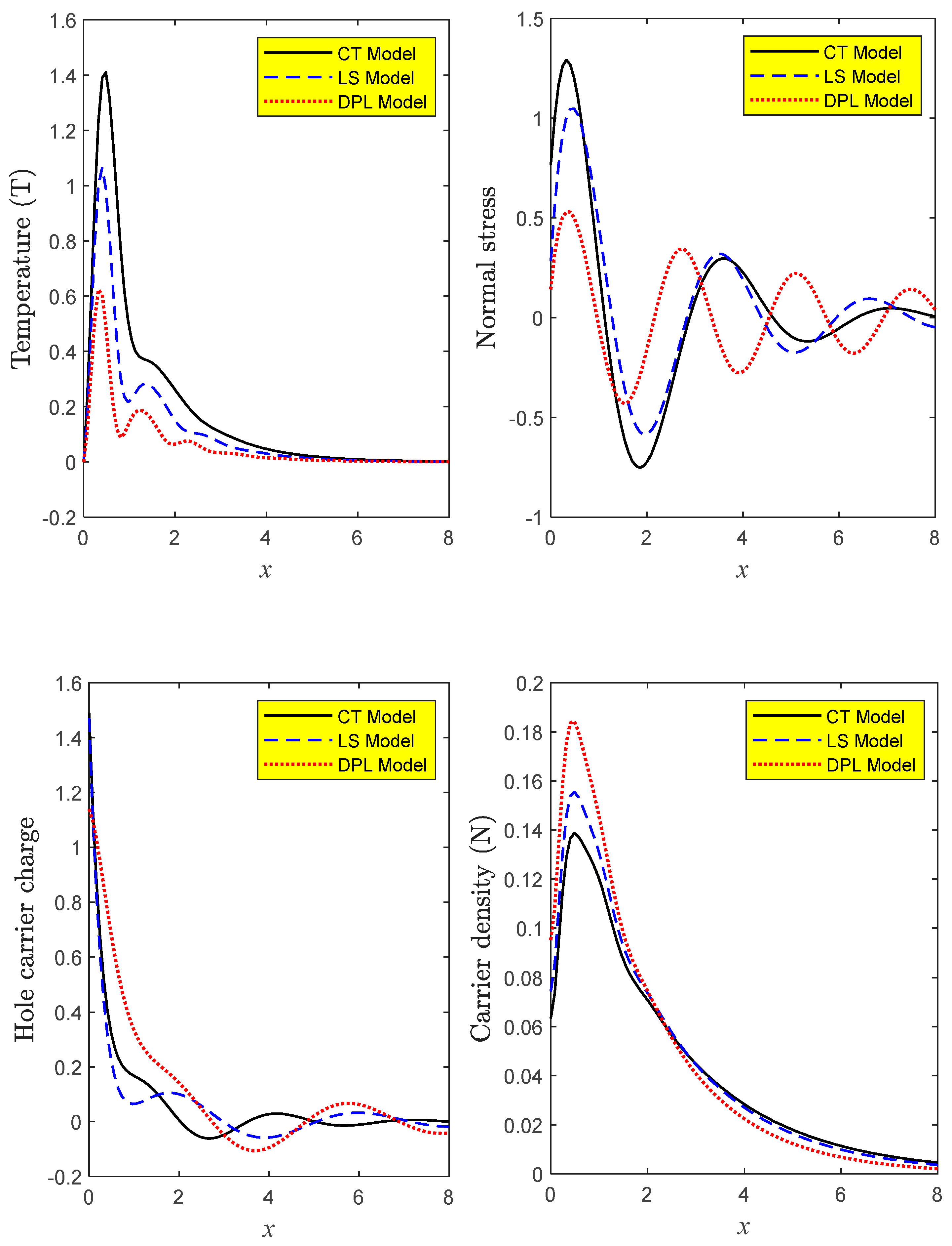
7.1. The Photo-Thermoelasticity Models

The distributions of the main real dimensionless fields along the axial direction at a short moment t = 0.02 are shown in the first group depicted in Figure 1. In order to describe the non-local photo-thermoelasticity models under the influence of a strong magnetic field and the Hall current effect, comparisons are made based on the variation of thermal relaxation times. With the help of the first subfigure, which depicts the isothermal condition that prevails at the non-local silicon medium’s outer surface, it is possible to study the dimensionless temperature distributions. The first subfigure shows how photo-thermal excitation and strong magnetic field pressure cause the dimensionless thermal wave values to start at their minimum value near the edge of the medium, and then increase with increasing distance until they approach the maximum value before decreasing gradually. On the other hand, the thermal wave propagates exponentially to approach zero inside the medium to reach the equilibrium state. The second subfigure shows the distributions of the dimensionless mechanical force or normal stress (mechanical wave) throughout the axial distance. The mechanical wave distributions meet the mechanical ramp-type requirement, which begins at a positive value on the edge of the non-local medium and progressively rises to a maximum value close to the surface (due to the pressure force of a strong magnetic field or Hall current). The mechanical wave progressively diminishes as it gets further from the outside surface, then increases and declines smoothly again as it approaches the zero line and seeks to attain equilibrium. The third subfigure shows how the thermal and elastic relaxation times affect the distributions of dimensionless hole carrier charges throughout the axial distance. The hole carrier charge distributions start from positive maximum values at the boundary edge of the non-local medium with a fast decrease to approach the minimum value during the processes of holes and plasma recombination. However, in the second range, the hole carrier charge distributions inside the material approach the stable situation for a brief period of time (as a result of the lack of excited electrons inside the material) before decreasing and becoming convergent to the zero line. According to the plasma recombination processes, the carrier density that represents the plasma waves (electron charge field distribution) starts from a positive value at the edge, as seen in the fourth subfigure. The optical-thermal energy and Hall current cause plasma waves to steadily increase towards the surface until they reach their maximum values. After briefly resting within the non-local semiconductor medium, they then begin to gradually decrease. In order to achieve stability, the plasma waves eventually start to get closer to the zero line. It adopts an exponentially significant behavior that is in line with the findings of the experiment.

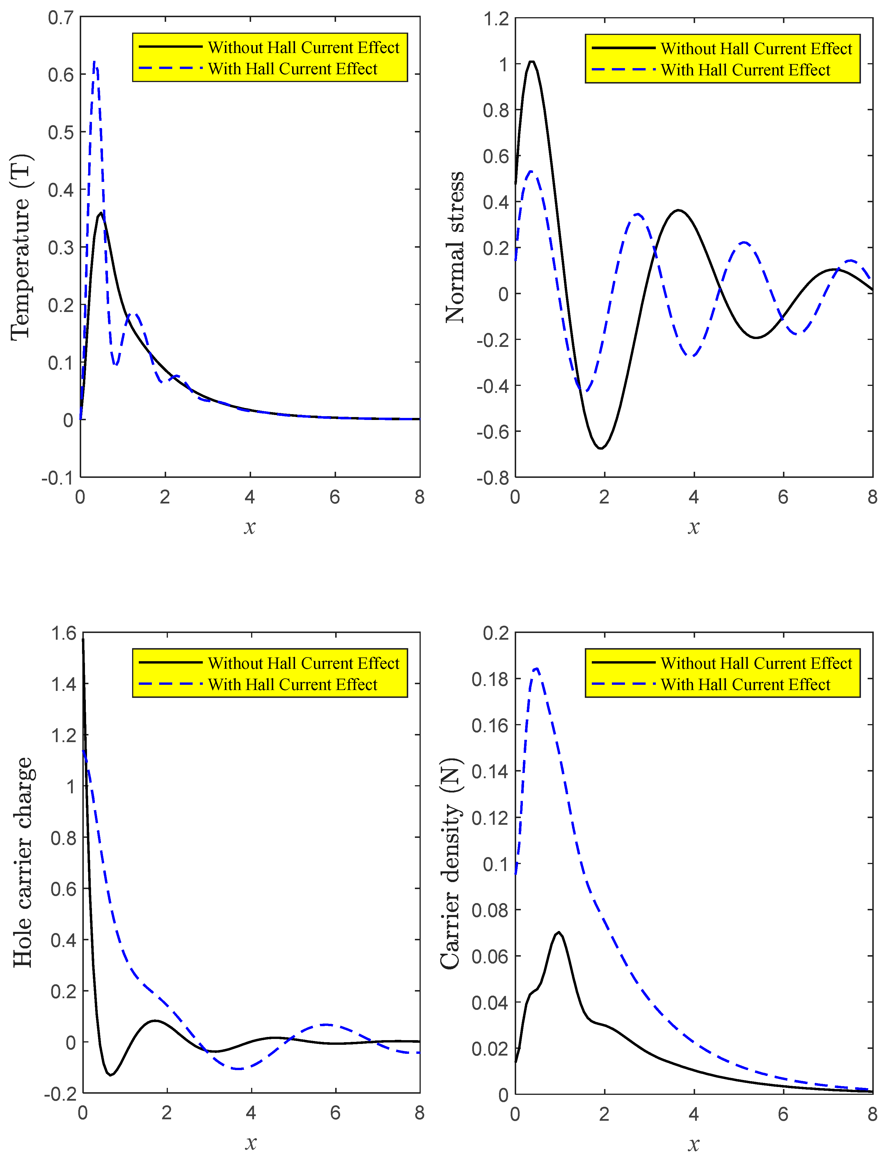
7.2. The Impact of Hall Current

The second group (Figure 2) shows how the principal fields ( T , σ , H , and N distributions) are affected by a strong magnetic field with a Hall current effect as a function of axial distance x . Two alternatives are investigated in this group using the DPL model for silicon non-local semiconductor material for small-time t = 0.02 . When the Hartmann number (the strength of magnetic pressure) has a value, the first example depicts the distribution of magnetic fields in the presence of the Hall current. The other depicts how physical fields are distributed when no significant magnetic field or Hall current are present. A cloud of surface electrons is created as a result of violent collisions between internal particles within the semiconductor medium caused by optical excitation and the compressive intensity of the strong magnetic field with the Hall current (plasma). This case deviates from the case of no magnetic excitation in terms of how all physical quantities propagate as waves. However, the inner particles (with the spin movement of particles) in the non-local semiconductor lattice are rearranged when a strong magnetic field with the Hall current is present. Increased holes and free electrons on the semiconductor’s outer surface as a result of the Hall current boost the flow of the electric current inside the semiconductor.

7.3. The Impact of Non-Local Parameter
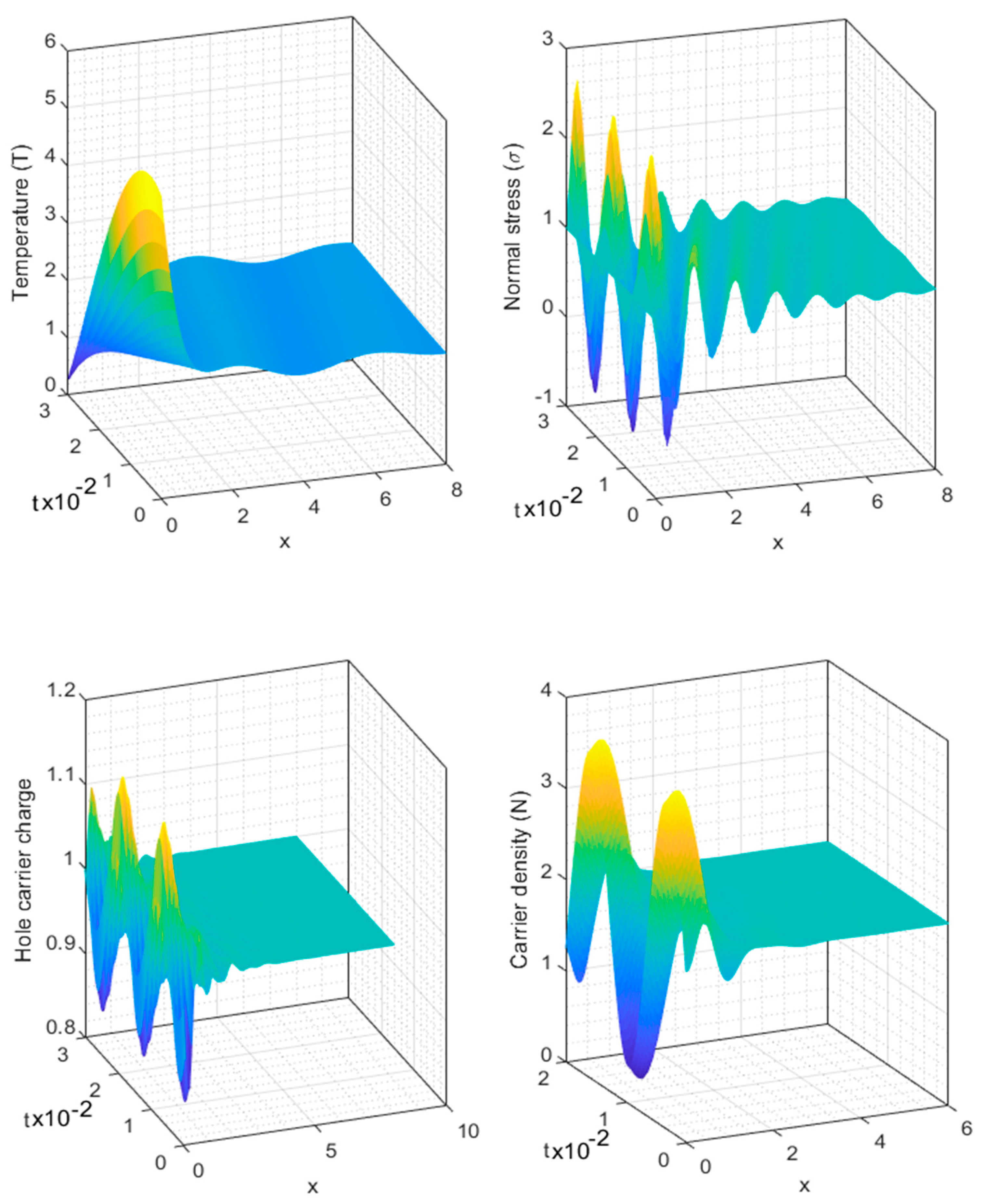
The third group (Figure 3) illustrates how a non-local parameter affects the main quantities ( T , σ , H , and N distributions) as a function of axial distance x . This group uses the DPL model to examine two possibilities while taking the influence of the Hall current for small-time t = 0.02 . The first example shows the non-locality semiconductor distribution when the non-local parameter ( ξ 1 0 ) has a value. The other illustrates the distribution of physical fields in the absence of a significant non-local parameter (local, ξ 1 = 0 ). From this group, it can be seen that all the field quantities under study exhibit a rise in non-locality. The temperature field is the lone exception. When compared to other distributions, the significance of the profile non-locality in temperature reduces. The non-locality remarkably influences all distributions. All physical fields are significantly impacted by non-locality. This is most likely caused by the following mechanism: to characterize the non-local effect on the distribution of the field variables of interest, the photo-elastic non-locality was introduced directly into the equation of motion and the constitutive equations rather than the heat conduction equation, as shown in the figures.

7.4. The 3D Graph

According to the DPL model for the non-local medium, Figure 4 (the fourth group) depicts three-dimensional (3D) graphs under the influence of a strong magnetic field and the Hall current effect. The variations of the wave distribution of fundamental physical quantities are examined in this figure in relation to changes in both time t and distance x . The dimensionless time t range can be obtained when 0 t 3 × 10 2   . With regard to this group, time variation has an impact on how waves spread across all physical fields that satisfy the boundary conditions. However, the axial distance and time scale variations affect how large the wave propagations are in all physical fields. According to the steady-state, we see that as distance and time increase, all wave propagation disappears and moves closer to the zero line.

8. Conclusions

In this research, the mathematical-physical models of non-local semiconductor materials are examined in the context of the creation of free charge carriers (electron–hole pairs) by electron excitation under the thermal influence of a light source. Here, a semiconducting material exposed to a strong magnetic field is used to study the thermal (temperature distribution), mechanical (normal stress distribution), and plasma (carrier electron/hole distribution) waves propagation. The newly developed model is based on the recombination of holes and electrons during elastic and electronic deformation in one dimension. The processes of optical energy and photo-excited diffusion are considered. Due to the pressure force of a strong magnetic field’s influence, the Hall current with a Hartmann number is obtained. The distribution of the physical fields’ wave propagation is impacted by the variations in relaxation time values. The wave propagation of the physical quantities under study is also impacted by the Hall current, which is a side effect of the strong magnetic field. This is because some materials, particularly non-local semiconductor materials, might undergo modifications as a result of the magnetic field, according to scientific theory. However, changes in time and distance affect how the main fields’ waves propagate. An example of an electromagnetic impact is the Hall influence. Scientists can therefore learn a great deal about semiconductors, linear Hall sensors, and Hall potentiometers by studying the Hall current. In numerous scientific disciplines, including automation technology, measurement technology, and electronics technology, the Hall effects are used extensively.

Author Contributions

Methodology, K.L.; Software, K.L. and A.A.E.-B.; Formal analysis, R.C.; Investigation, R.C.; Resources, K.L.; Data curation, R.C. and M.M.A.; Writing—original draft, M.M.A.; Writing—review & editing, M.M.A.; Visualization, A.A.E.-B.; Supervision, K.L. All authors have read and agreed to the published version of the manuscript.

Funding

This research received no external funding.

Data Availability Statement

The information applied in this research is ready from the author upon request.

Conflicts of Interest

The authors declare no conflict of interest.

Nomenclature

λ ,     μ Counterparts of Lame’s parameters,
n 0 Equilibrium carrier concentration (electrons concentration)
h 0 Equilibrium holes concentration
T 0   Absolute temperature
γ = ( 3 λ + 2 μ ) α t The volume coefficient of thermal expansion
σ ij Components of the stress tensor
ρ Density of the medium
α h , α n Holes and electrons thermo-diffusive parameters
τ θ ,     τ q The elastic and thermal relaxation times
t n , t h The electrons and holes relaxation times
α t The coefficient of linear thermal expansion
τ q The elastic relaxation time
τ θ Thermal relaxation time
C e Specific heat at constant strain of the medium
K The thermal conductivity of the medium
τ * The photogenerated carrier lifetime
E g The energy gap of the medium of semiconductor
δ n = ( 2 μ + 3 λ ) d n The electrons elasto-diffusive parameter
δ h = ( 2 μ + 3 λ ) d h The holes elasto-diffusive parameter
d n The coefficients of electronic deformation
d h The coefficients of hole deformation
m n q , m q n , m h q , m q h Peltier-Dufour- Seebeck-Soret-like constants
D n , D h The diffusion coefficients of the electrons and holes
a Q n , a Q h , a Q , a n ,   a h The flux-like constants

References

  1. Hall, E.H. On a New Action of the Magnet on Electric Currents. Am. J. Math. 1879, 2, 287–292. [Google Scholar] [CrossRef]
  2. Biot, M.A. Thermoelasticity and irreversible thermodynamics. J. Appl. Phys. 1956, 27, 240–253. [Google Scholar] [CrossRef]
  3. Lord, H.; Shulman, Y. A generalized dynamical theory of Thermoelasticity. J. Mech. Phys. Solids 1967, 15, 299–309. [Google Scholar] [CrossRef]
  4. Green, A.E.; Lindsay, K.A. Thermoelasticity. J. Elast. 1972, 2, 1–7. [Google Scholar] [CrossRef]
  5. Chandrasekharaiah, D.S. Thermoelasticity with second sound: A review. Appl. Mech. Rev. 1986, 39, 355–376. [Google Scholar] [CrossRef]
  6. Chandrasekharaiah, D.S. Hyperbolic Thermoelasticity: A review of recent literature. Appl. Mech. Rev. 1998, 51, 705–729. [Google Scholar] [CrossRef]
  7. Sharma, J.N.; Kumar, V.; Dayal, C. Reflection of generalized thermoelastic waves from the boundary of a half-space. J. Therm. Stresses 2003, 26, 925–942. [Google Scholar] [CrossRef]
  8. Lotfy, K.; Abo-Dahab, S. Two-dimensional problem of two temperature generalized thermoelasticity with normal mode analysis undethermal shock problem. J. Comput. Theor. Nanosci. 2015, 12, 1709–1719. [Google Scholar] [CrossRef]
  9. Othman, M.; Lotfy, K. The influence of gravity on 2-D problem of two temperature generalized thermoelastic medium with thermal relaxation. J. Comput. Theor. Nanosci. 2015, 12, 2587–2600. [Google Scholar] [CrossRef]
  10. Maruszewski, B. Electro-magneto-thermo-elasticity of Extrinsic Semiconductors, Classical Irreversible Thermodynamic Approach. Arch. Mech. 1986, 38, 71–82. [Google Scholar]
  11. Maruszewski, B. Electro-magneto-thermo-elasticity of Extrinsic Semiconductors, Extended Irreversible Thermodynamic Approach. Arch. Mech. 1986, 38, 83–95. [Google Scholar]
  12. Maruszewski, B. Coupled Evolution Equations of Deformable Semiconductors. Int. J. Engr. Sci. 1987, 25, 145–153. [Google Scholar] [CrossRef]
  13. Sharma, J.N.; Thakur, N.T. Plane harmonic elasto-thermodiffusive waves in semiconductor materials. J. Mech. Mater. Struct. 2006, 1, 813–835. [Google Scholar] [CrossRef] [Green Version]
  14. Mandelis, A. Photoacoustic and Thermal Wave Phenomena in Semiconductors; Elsevier: New York, NY, USA, 1987. [Google Scholar]
  15. Almond, D.; Patel, P. Photothermal Science and Techniques; Springer Science & Business Media: Berlin, Germany, 1996. [Google Scholar]
  16. Gordon, J.P.; Leite, R.C.C.; Moore, R.S.; Porto, S.P.S.; Whinnery, J.R. Long-transient effects in lasers with inserted liquid samples. Bull. Am. Phys. Soc. 1964, 119, 501. [Google Scholar] [CrossRef]
  17. Lotfy, K. Effect of variable thermal conductivity during the photothermal diffusion process of semiconductor medium. Silicon 2019, 11, 1863–1873. [Google Scholar] [CrossRef]
  18. Lotfy, K.; Tantawi, R.S. Photo-thermal-elastic interaction in a functionally graded material (FGM) and magnetic field. Silicon 2020, 12, 295–303. [Google Scholar] [CrossRef]
  19. Lotfy, K. A novel model of magneto photothermal diffusion (MPD) on polymer nano-composite semiconductor with initial stress. Waves Ran. Comp. Med. 2021, 31, 83–100. [Google Scholar] [CrossRef]
  20. Lotfy, K.; El-Bary, A.A.; Hassan, W.; Ahmed, M.H. Hall current influence of microtemperature magneto-elastic semiconductor material. Superlattices Microstruct. 2020, 139, 106428. [Google Scholar] [CrossRef]
  21. Mahdy, A.M.S.; Lotfy, K.; Ahmed, M.H.; El-Bary, A.; Ismail, E.A. Electromagnetic Hall current effect and fractional heat order for microtemperature photo-excited semiconductor medium with laser pulses. Results Phys. 2020, 17, 103161. [Google Scholar] [CrossRef]
  22. Mahdy, A.M.S.; Lotfy, K.; El-Bary, A.; Tayel, I.M. Variable thermal conductivity and hyperbolic two-temperature theory during magneto-photothermal theory of semiconductor induced by laser pulses. Eur. Phys. J. Plus 2021, 136, 651. [Google Scholar] [CrossRef]
  23. Lotfy, K. The elastic wave motions for a photothermal medium of a dual-phase-lag model with an internal heat source and gravitational field. Can. J. Phys. 2016, 94, 400–409. [Google Scholar] [CrossRef] [Green Version]
  24. Lotfy, K. A Novel Model of Photothermal Diffusion (PTD) fo Polymer Nano- composite Semiconducting of Thin Circular Plate. Phys. B Condens. Matter 2018, 537, 320–328. [Google Scholar] [CrossRef]
  25. Lotfy, K.; Kumar, R.; Hassan, W.; Gabr, M. Thermomagnetic effect with microtemperature in a semiconducting Photothermal excitation medium. Appl. Math. Mech. Engl. Ed. 2018, 39, 783–796. [Google Scholar] [CrossRef]
  26. Mahdy, A.M.S.; Lotfy, K.; El-Bary, A.; Sarhan, H.H. Effect of rotation and magnetic field on a numerical-refined heat conduction in a semiconductor medium during photo-excitation processes. Eur. Phys. J. Plus 2021, 136, 553. [Google Scholar] [CrossRef]
  27. Lotfy, K. A novel model for Photothermal excitation of variable thermal conductivity semiconductor elastic medium subjected to mechanical ramp type with two-temperature theory and magnetic field. Sci. Rep. 2019, 9, 3319. [Google Scholar] [CrossRef]
  28. Zhou, H.; Shao, D.; Li, P. Thermoelastic damping and frequency shift in micro/nano-ring resonators considering the nonlocal single-phase-lag effect in the thermal field. Appl. Math. Model. 2022, 115, 237–258. [Google Scholar] [CrossRef]
  29. Lata, P.; Singh, S. Effects of Hall current and nonlocality in a magneto-thermoelastic solid with fractional order heat transfer due to normal load. J. Therm. Stress. 2022, 45, 51–64. [Google Scholar] [CrossRef]
  30. Marin, M. A domain of influence theorem for microstretch elastic materials. Nonlinear Anal. Real World Appl. 2010, 11, 3446–3452. [Google Scholar] [CrossRef]
  31. Marin, M. A partition of energy in thermoelasticity of microstretch bodies. Nonlinear Anal. Real World Appl. 2010, 11, 2436–2447. [Google Scholar] [CrossRef]
  32. Abbas, I.; Marin, M. Analytical Solutions of a Two-Dimensional Generalized Thermoelastic Diffusions Problem Due toLaser Pulse. Iran. J. Sci. Technol.-Trans. Mech. Eng. 2018, 42, 57–71. [Google Scholar] [CrossRef]
  33. Mondal, S.; Sur, A. Photo-thermo-elastic wave propagation in anorthotropic semiconductor with a spherical cavity and memory responses. Wavesin Random Complex Media 2021, 42, 1835–1858. [Google Scholar] [CrossRef]
  34. Abbas, I.; Alzahranib, F.; Elaiwb, A. A DPL model of photothermal interaction in a semiconductor material. Waves Random Complex Media 2019, 29, 328–343. [Google Scholar] [CrossRef]
  35. Mustafa, F.; Hashim, A.M. Plasma Wave Electronics: A Revival Towards Solid-State Terahertz Electron Devices. J. Appl. Sci. 2010, 10, 1352–1368. [Google Scholar] [CrossRef] [Green Version]
  36. Alhejaili, W.; Lotfy, K.; El-Bary, A. Photo–elasto–thermodiffusion waves of semiconductor with ramp-type heating for electrons–holes-coupled model with initial stress. Waves Random Complex Media 2022, 1–19. [Google Scholar] [CrossRef]
Scheme 1. Schematic of the problem.
Crystals 12 01680 sch001
Figure 1. The key physical distributions’ variation in relation to distance under the influence of Hall current and non-local parameters, as predicted by photo-thermoelasticity models.
Crystals 12 01680 g001
Figure 2. In both the presence and absence of the Hall current effect, the main field distributions against distance vary, according to the DPL model in non-local case.
Crystals 12 01680 g002
Figure 3. According to the DPL model with the influence of Hall current, the primary field distributions against distance change in both the presence and absence of the non-local parameter.
Crystals 12 01680 g003
Figure 4. According to the DPL model and under the influence of Hall current, the principal fields in 3D plots for non-local Si material vary with variations in time and distance.
Crystals 12 01680 g004
Table 1. The physical parameters of Si material in SI units.
UnitSymbolValue
N / m 2 λ
μ
6.4 × 10 10
6.5 × 10 10
kg / m 3 ρ 2330  
K T 0 800
sec   ( s ) τ   5 ×   10 5
K 1 α t   4.14 ×   10 6
  Wm 1 K 1 k   150  
J / ( kg   K ) C e 695  
  m / s s ˜ 2
H / m μ 0 4 π × 10 7
VK 1 m q n 1.4 × 10 5
m n q 1.4 × 10 5
m q h 0.004 × 10 6
m h q 0.004 × 10 6
m 2 s 1 D n 0.35 × 10 2
m 2 s 1 D h 0.125 × 10 2
m 2 / s α n 1 × 10 2
m 2 / s α h 5 × 10 3
Publisher’s Note: MDPI stays neutral with regard to jurisdictional claims in published maps and institutional affiliations.

